I3C Controller overview
Features List
Controller Core Logic
The foundation of the I3C Host Controller, handling standard bus operations, arbitration, and framing.
Frame Generation: Support for SDR Read and Write transactions, both with and without the
7'h7EI3C broadcast address.Bus Speed Configurability: Dynamic control over bus operating frequencies (for both Open-Drain and Push-Pull modes) via dedicated timing CSRs.
SDA Arbitration Management: Autonomous handling of bus arbitration during address phase.
In-Band Interrupt (IBI) Detection: Hardware-level detection and processing of target-initiated IBIs.
HDR Pattern Generation: Includes logic to generate the specific sequence required to exit High Data Rate (HDR) modes, ensuring proper bus reset and compatibility.
Error Handling: Built-in Target Error Detection and Escalation mechanisms.
Dynamic Address Assignment (DAA)
The controller fully implements DAA according to the bus initialization sequence defined in the I3C Basic Specification (Section 5.1.4.2) and the I3C HCI Specification (Section 8.4.1.1) for the ENTDAA command.
Software Configuration Guidelines:
Pre-populate the DAT: All Device Address Table (DAT) entries for targets awaiting a dynamic address must be fully populated before sending the
ENTDAAcommand.Handling Unassigned Targets: If the
DEV_COUNTlimit is reached but unaddressed devices remain on the bus, the controller signals this by returning0x1in theDATA_LENGTHfield of the Response Descriptor.DCT Initialization: The Device Characteristics Table (DCT) Index always starts at
0.
In-Band Interrupts (IBI)
The controller supports the detection, validation, and servicing of IBIs initiated by targets, whether raised during a Bus Available condition or during arbitrable address headers.
Reverse Lookup & Validation: When a target drives its dynamic address during an IBI request, a hardware reverse lookup table quickly resolves it to a DAT index.
IBI Rejection: The controller automatically rejects the IBI (NACK) if the bitwise condition
IBI_REJECT | ~IBI_PAYLOADis met. This ensures interrupts are ignored ifIBI_REJECTis set (1), or if the target is not authorized to send payloads (IBI_PAYLOADis0).Data Packing: Accepted IBI data is efficiently packed into the 32-bit
PIOCONTROL.IBI_PORTCSR for host software:Status Descriptor: The first DWORD contains metadata (payload
data_lengthand target dynamic address).Mandatory Data Byte (MDB): If present, the MDB is packed into the Least Significant Byte (LSB) of the very first data DWORD following the descriptor.
Payload Data: The remaining payload is chunked and written as
(data_length + 3) / 4DWORDs.
Overflow Handling: The controller uses an internal hardware buffer for optional IBI payload bytes. If a target sends data equal to or exceeding this buffer size, the controller aborts the transaction, flags an error, and writes only the successfully captured bytes (up to the buffer limit) into the
IBI_PORT.
Common Command Codes (CCC)
Support for the essential subset of CCCs required for basic bus management, initialization, and device configuration.
Broadcast Support
ENEC: Enable Events Command (Broadcast).
DISEC: Disable Events Command (Broadcast).
RSTDAA: Reset Dynamic Address Assignment (Broadcast).
ENTDAA: Enter Dynamic Address Assignment (Broadcast).
SETAASA: Set All Addresses to Static Address (Broadcast).
Direct Support
ENEC: Enable Events Command (Direct).
DISEC: Disable Events Command (Direct).
SETDASA: Set Dynamic Address from Static Address (Direct).
SETNEWDA: Set New Dynamic Address (Direct).
GETPID: Get Provisional ID (Direct).
GETBCR: Get Bus Characteristics Register (Direct).
GETDCR: Get Device Characteristics Register (Direct).
Host Controller Interface (HCI)
The software-to-hardware interface bridging the driver to the I3C Core logic.
Registers (RDL): Full implementation of the Register Description List for configuration and status monitoring.
Queues: Dedicated memory-mapped queues for Command, Response, TX, RX, and IBI data.
Hardware Tables:
DAT (Device Address Table): Storage for dynamic addresses, rejection logic, and device types.
DCT (Device Characteristics Table): Storage for target-specific physical parameters (PID, BCR, DCR).
Error Conditions
The controller supports the following hardware ERROR_STATUS conditions, derived from Table 1 (Error Status Codes in Response Descriptor) of the I3C TCRI Spec.
Error Code |
ERR_STATUS Value |
I3C TCRI Spec Section |
Notes |
|---|---|---|---|
CRC |
0x1 |
6.4.1.1 |
|
PARITY |
0x2 |
6.4.1.2 |
|
FRAME |
0x3 |
6.4.1.3 |
|
ADDR_HEADER |
0x4 |
6.4.1.4 |
|
NACK |
0x5 |
6.4.1.5 |
|
OVL |
0x6 |
6.4.1.6 |
|
I3C_SHORT_READ_ERR |
0x7 |
6.4.1.7 |
|
HC_ABORTED |
0x8 |
6.4.1.8 |
|
I2C_WR_DATA_NACK or BUS_ABORTED |
0x9 |
6.4.1.9 |
|
NOT_SUPPORTED |
0xA |
6.4.1.10 |
|
ABORTED_WITH_CRC |
0xB |
6.4.1.11 |
Used as an internal default state for errors. Internal hardware bugs may mistakenly produce this status. |
Transfer Type Specific |
0xC – 0xF |
6.4.1.12 |
Architecture
The design is partitioned into two primary subsystems: the Host Controller Interface (HCI) and the Host Controller (HC). These subsystems communicate via command/response queues and shared lookup tables (DAT/DCT).
High-Level Block Diagram
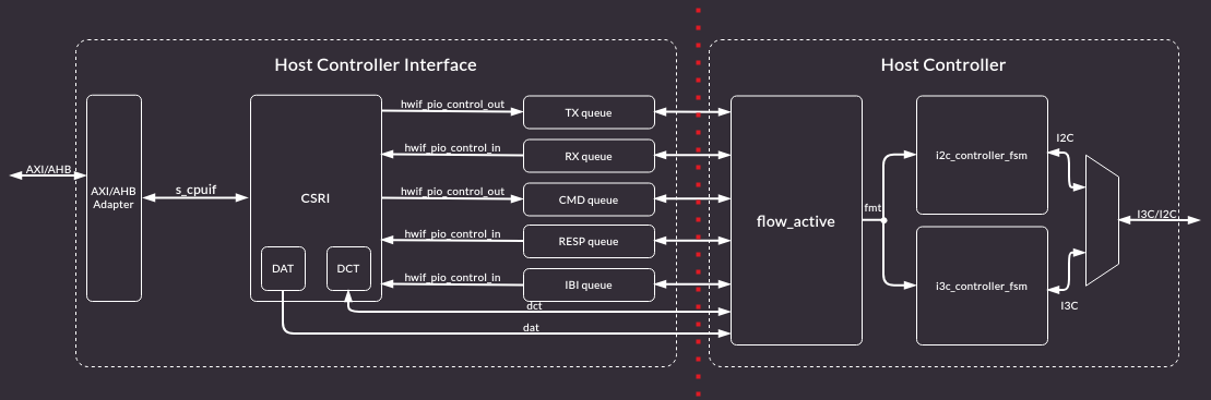
Figure 1 High-Level Block Diagram
Subsystems
HCI (Host Controller Interface):
Interface: AXI/AHB (Slave interface).
Function: Handles communication with the Host CPU. It populates Control and Status Registers (CSRs) and transfers relevant information between the CSRs and the internal hardware queues (Command, Response, TX, RX, IBI).
HC (Host Controller):
Function: Reads operational data from the queues and translates them into physical I3C transactions (driving SDA/SCL output signals).
Components: Consists of the
flow_activemodule (protocol logic) and the low-level PHY FSMs (i3c_controller_fsm/i2c_controller_fsm).
Data Flow
Command Generation: Software writes commands to HCI CSRs.
Queue Population: HCI logic pushes these commands into the Command Queue.
Execution: HC fetches commands, consults the Device Address Table (DAT) or Device Characteristics Table (DCT), and executes the transaction on the bus.
Response: Results are written back to the Response Queue for software to read.
Microarchitecture
The Host Controller (HC) logic is split into a “decode” stage (Flow Active FSM) and “execute” stage (i3c/i2c controller FSM).
flow_active (Decode FSM)
This module acts as a decoder. It consumes raw data from queues and converts it into control signals (fmt_* signals) for the downstream controller FSMs.
Control and data are handled strictly in 9-bit blocks (1 byte + T-bit/ACK). Once the sending or receiving of a 9-bit block begins, the process cannot be aborted halfway through.
Operating Principle
Interfaces:
Upstream: Read/Write access to HCI Queues (Cmd, Resp, Tx, Rx, IBI).
Downstream:
fmtinterface (fmt_byte_o+ flags) toi2c_controller_fsm/i3c_controller_fsm.
Operating Principle:
Operates in PIO Mode (Programmed I/O) using SDR (Standard Data Rate).
fmt_byte_ois the data, that will be sent on the I3C bus.
FSM States & Transitions:
Idle: Waits for
i3c_fsm_en_isignal indicating a new command is present in the Command Queue or IBI to wake up FSM.WaitForCmd: Fetches the 64-bit Command Descriptor from the Command Queue.
FetchDAT: Retrieves the Device Address Table (DAT) entry corresponding to the command’s Device Index. Transitions to the execution stage based on
cmd_attr(Command Attribute).Execution:
I2C Write Immediate / I3C Write Immediate: uses immediate command descriptor format and reads data directly from the command descriptor.
I2C Write Regular / I3C Write Regular: uses regular command descriptor format and reads data from TX Queue
I2C Read / I3C Read: uses regular command descriptor format and writes data into RX Queue
WriteResp: Generates a Response Descriptor, loads it into the Response Queue, and returns to Idle.
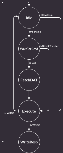
Figure 2 Flow Active FSM
Signal List
Signal |
Direction |
Width |
Description |
|
input |
1 |
Clock |
|
input |
1 |
Active low reset |
|
input |
1 |
Command FIFO queue full flag |
|
input |
|
Command FIFO ready threshold |
|
input |
1 |
Command FIFO ready threshold trigger |
|
input |
1 |
Command FIFO empty flag |
|
input |
1 |
Command FIFO read valid |
|
output |
1 |
Command FIFO read ready |
|
input |
|
Command FIFO read data |
|
input |
1 |
RX FIFO queue full flag |
|
input |
|
RX FIFO start threshold |
|
input |
1 |
RX FIFO start threshold trigger |
|
input |
|
RX FIFO ready threshold |
|
input |
1 |
RX FIFO ready threshold trigger |
|
input |
1 |
RX FIFO empty flag |
|
output |
1 |
RX FIFO write valid |
|
input |
1 |
RX FIFO write ready |
|
output |
|
RX FIFO write data |
|
input |
1 |
TX FIFO queue full flag |
|
input |
|
TX FIFO start threshold |
|
input |
1 |
TX FIFO start threshold trigger |
|
input |
|
TX FIFO ready threshold |
|
input |
1 |
TX FIFO ready threshold trigger |
|
input |
1 |
TX FIFO empty flag |
|
input |
1 |
TX FIFO read valid |
|
output |
1 |
TX FIFO read ready |
|
input |
|
TX FIFO read data |
|
input |
1 |
Response FIFO queue full flag |
|
input |
|
Response FIFO ready threshold |
|
input |
1 |
Response FIFO ready threshold trigger |
|
input |
1 |
Response FIFO empty flag |
|
output |
1 |
Response FIFO write valid |
|
input |
1 |
Response FIFO write ready |
|
output |
|
Response FIFO write data |
|
input |
1 |
IBI FIFO queue full flag |
|
input |
|
IBI FIFO ready threshold |
|
input |
1 |
IBI FIFO ready threshold trigger |
|
input |
1 |
IBI FIFO empty flag |
|
output |
1 |
IBI FIFO write valid |
|
input |
1 |
IBI FIFO write ready |
|
output |
|
IBI FIFO write data |
|
input |
|
DAT memory interface |
|
output |
1 |
DAT read valid HW |
|
output |
|
DAT index HW |
|
input |
64 |
DAT read data HW |
|
output |
1 |
DCT write valid HW |
|
output |
1 |
DCT read valid HW |
|
output |
|
DCT index HW |
|
output |
128 |
DCT write data HW |
|
input |
128 |
DCT read data HW |
|
output |
1 |
Enable host functionality |
|
output |
1 |
Is an I2C transfer flag |
|
input |
1 |
I2C command complete flag |
|
input |
1 |
PHY select OD/PP input |
|
output |
1 |
PHY select OD/PP output |
|
output |
1 |
Format FIFO read valid |
|
output |
|
Format FIFO depth |
|
input |
1 |
Format FIFO read ready |
|
input |
1 |
Format FIFO read done |
|
output |
8 |
Format TX byte output |
|
output |
1 |
Format TX bit output (T bit) |
|
output |
1 |
Format flag: start before |
|
output |
1 |
Format flag: restart after |
|
output |
1 |
Format flag: stop after |
|
output |
1 |
Format flag: read continue |
|
input |
1 |
Format receive NACK |
|
input |
1 |
SDA line arbitration is detected |
|
input |
8 |
Format RX byte input |
|
input |
1 |
Format RX bit input |
|
output |
1 |
Format flag: read bytes |
|
input |
1 |
Format flag: read valid |
|
output |
1 |
Format flag: NAK OK |
|
output |
1 |
Format flag: HDR exit |
|
output |
1 |
Unhandled unexpected NAK |
|
output |
1 |
Unhandled NAK timeout |
|
input |
1 |
I2C Controller RX FIFO write valid |
|
input |
|
I2C Controller RX FIFO write data |
|
input |
1 |
I3C FSM enable |
|
output |
1 |
I3C FSM idle status |
|
input |
1 |
PIO RS input |
|
input |
1 |
Halt on command sequence timeout |
|
input |
1 |
HC_CONTROL.RESUME CSR field |
|
input |
1 |
HC_CONTROL.ABORT | PIO_CONTROL.ABORT CSR fields |
|
output |
|
I3C Error structure |
|
output |
|
I3C Interrupt structure |
i3c_controller_fsm (Execute / Timing FSM for I3C)
This module acts as the main controller of the I3C bus, handling the serialization of data and generation of the Start (S), Stop (P) and repeated Start (Sr) conditions. It also handles switching between Open Drain mode and Push Pull mode, also respecting the different timing requirements (See 6.2 Timing Specification I3C Basic Spec).
Operating Principle
Function:
Consumes
fmtsignals (byte data + control flags like Start/Stop/Nak) from theflow_activemodule.Drives physical SDA and SCL lines.
Timing FSM: Generates the SCL clock based on I3C SDR timing requirements (in Open Drain and Push Pull mode).
Serialization: Serializes the
fmt_byteonto the SDA line for write transactions.Parallelization: Parallelizes received data into a
fmt_bytefor theflow_activemodule for read transactions.Protocol Framing: Reacts to
fmt_flag_startandfmt_flag_stopto generate Start/Stop conditions, as well asfmt_flag_restartto generate a repeated Start condition.
Signal List
Signal |
Direction |
Width |
Description |
|
input |
1 |
Clock |
|
input |
1 |
Active low reset |
|
input |
1 |
Interface to SCL input |
|
input |
1 |
Interface to SDA input |
|
output |
1 |
Interface to SCL output |
|
output |
1 |
Interface to SDA output |
|
input |
|
Bus state |
|
output |
1 |
PHY select Open-Drain/Push-Pull output |
|
input |
1 |
Is I2C transfer flag |
|
input |
|
High period of the SCL in clock units |
|
input |
|
Low period of the SCL in clock units |
|
input |
|
High period of the SCL in clock units (Open-Drain Mode) |
|
input |
|
High period of the SCL in clock units (Open-Drain Mode during init procedure) |
|
input |
|
Low period of the SCL in clock units (Open-Drain Mode) |
|
input |
|
Rise time of both SDA and SCL in clock units |
|
input |
|
Fall time of both SDA and SCL in clock units |
|
input |
|
Hold time for START in clock units (Open-Drain Mode) |
|
input |
|
Hold time for repeated START in clock units |
|
input |
|
Setup time for repeated START in clock units |
|
input |
|
Setup time for STOP in clock units |
|
input |
|
Setup time for SDA during START in clock units (Open-Drain Mode) |
|
input |
|
Data setup time in clock units |
|
input |
|
Data hold time in clock units |
|
input |
|
Bus free time between STOP and START in clock units |
|
input |
|
Bus IDLE condition time in clock units |
|
input |
|
Bus AVAILABLE condition time in clock units |
|
input |
1 |
Format FIFO read valid |
|
output |
1 |
Format FIFO read ready |
|
output |
1 |
Format FIFO read done |
|
input |
8 |
Format TX byte input |
|
input |
1 |
Format TX bit input (T bit) |
|
input |
1 |
Format flag: start before |
|
input |
1 |
Format flag: stop after |
|
input |
1 |
Format flag: restart after |
|
output |
1 |
Format receive NACK |
|
output |
1 |
SDA line arbitration is detected |
|
output |
8 |
Format RX byte output |
|
output |
1 |
Format RX bit output (T bit) |
|
input |
1 |
Format flag: read bytes |
|
input |
1 |
Format flag: read continue |
|
output |
1 |
Format flag: read valid |
|
input |
1 |
Format flag: HDR exit |
i2c_controller_fsm (Execute / Timing FSM for I2C)
This module acts as the main controller of the I2C bus, handling the serialization of data and generation of the Start (S), Stop (P) and repeated Start (Sr) conditions. It handles the I2C timing requirements (See 6.2 Timing Specification I3C Basic Spec). Note that all transactions in I2C are in Open Drain mode. This module is taken from the Open Titan I2C Core.
Operating Principle
Function:
Consumes
fmtsignals (byte data + control flags like Start/Stop/Nak) from theflow_activemodule.Drives physical SDA and SCL lines.
Timing FSM: Generates the SCL clock based on I3C SDR timing requirements (in Open Drain and Push Pull mode).
Serialization: Serializes the
fmt_byteonto the SDA line for write transactions.Parallelization: Parallelizes received data into a
fmt_bytefor theflow_activemodule for read transactions.Protocol Framing: Reacts to
fmt_flag_startandfmt_flag_stopto generate Start/Stop conditions. (Differently to thei3c_controller_fsmthis module does not have afmt_repeated_startflag. It generates a repeated start by setting thefmt_flag_start.)
Signal List
Signal |
Direction |
Width |
Description |
|
input |
1 |
Clock |
|
input |
1 |
Active low reset |
|
input |
1 |
Interface to SCL input |
|
output |
1 |
Interface to SCL output |
|
input |
1 |
Interface to SDA input |
|
output |
1 |
Interface to SDA output |
|
input |
1 |
Enable host functionality |
|
input |
1 |
Indicates there is valid data in format FIFO |
|
input |
|
Format FIFO depth |
|
output |
1 |
Populates format FIFO |
|
input |
8 |
Byte in format FIFO to be sent to target |
|
input |
1 |
Issue START before sending byte |
|
input |
1 |
Issue STOP after sending byte |
|
input |
1 |
Indicates byte is a number of reads |
|
input |
1 |
Host to send ACK to final byte read |
|
input |
1 |
No ACK is expected |
|
input |
1 |
Unhandled unexpected NAK |
|
input |
1 |
NACK handler timeout event not cleared |
|
output |
1 |
High if there is valid data in RX FIFO |
|
output |
|
Byte in RX FIFO read from target |
|
output |
1 |
Indicates the host is idle |
|
input |
|
High period of the SCL in clock units |
|
input |
|
Low period of the SCL in clock units |
|
input |
|
Rise time of both SDA and SCL in clock units |
|
input |
|
Fall time of both SDA and SCL in clock units |
|
input |
|
Hold time for (repeated) START in clock units |
|
input |
|
Setup time for repeated START in clock units |
|
input |
|
Setup time for STOP in clock units |
|
input |
|
Data setup time in clock units |
|
input |
|
Data hold time in clock units |
|
input |
|
Bus free time between STOP and START in clock units |
|
input |
31 |
Max time target connected to this host may stretch the clock (UNUSED) |
|
input |
1 |
Assert if target stretches clock past max (UNUSED) |
|
input |
31 |
Timeout threshold for unhandled Host-Mode ‘nak’ IRQ (UNUSED) |
|
input |
1 |
Enable for host NACK handler timeout |
|
output |
1 |
Target didn’t ACK when expected (UNUSED) |
|
output |
1 |
SW didn’t handle the NACK in time (UNUSED) |
|
output |
1 |
Other device forcing SCL low (UNUSED) |
|
output |
1 |
Other device forcing SDA low (UNUSED) |
|
output |
1 |
Target stretches clock past max time (UNUSED) |
|
output |
1 |
SDA is not constant during SCL pulse (UNUSED) |
|
output |
1 |
Command is complete |
SRAM Macros
The internal memory structures for the Device Address Table (DAT) and Device Characteristic Table (DCT) are implemented using the OpenTitan generic single-port RAM macro (prim_generic_ram_1p).
This parameterized module provides standard wrapper for synchronous single-port SRAM instantiation. The source code for this macro can be referenced in the i3c-core repository: prim_generic_ram_1p.sv.
Memory Block |
Width (Bits) |
Depth (Words) |
Size |
DAT (Device Address Table) |
64 |
32 |
2 kbit |
DCT (Device Characteristic Table) |
128 |
32 |
4 kbit |