Specification for I3C Vendor-Specific Extended Capabilities
This chapter provides a description of Target Transaction Interface that created for the Standby Controller according to the normative specification of the Vendor-Specific Extended Capabilities for the I3C Controller as per section 7.7.13 of the I3C HCI spec.
Security
The HCI specification defines Extended Capabilities as a list of linked lists, which can be discovered from software through a series of CSR reads. This mechanism is unacceptable for the Recovery Mode as memory offsets must be known at synthesis time. Implementation based on this specification should provide a list of known memory offsets for each of the Extended Capabilities.
Note
In order to increase security of the solution, the offsets are provided, so software may choose to skip the discovery mechanism. This specification is compliant with the original specification, so the mechanism of discovery can still be used, if needed.
Extended Capabilities
Standby Controller Mode - 0x12
The Standby Controller Mode follows the I3C HCI spec:
Chapter 6 Theory of Operation
Section 6.17 Standby Controller Mode
Chapter 7 Register Interface
Section 7.7.11 Standby Controller Mode
Vendor-specific Extended Capabilities
This specification provides definitions and descriptions of the following Capabilities:
Controller Config
Standby Controller Mode
Secure Firmware Recovery Interface
Target Transaction Interface
SoC Management Interface
Extended Capability |
ID |
Memory Offset |
Controller Config |
0x02 |
Implementer |
Standby Controller Mode |
0x12 |
Implementer |
Secure Firmware Recovery Interface |
0xC0 |
Implementer |
SoC Management Interface |
0xC1 |
Implementer |
Target Transaction Interface |
0xC4 |
Implementer |
Controller Config - 0x02
The Controller Config Capability follows section 7.7.3 of the I3C HCI spec.
Secure Firmware Recovery Interface - 0xC0
This section is based on the Open Compute Project Secure Firmware Recovery, Version 1.1-rc5 and the I3C Target Recovery Specification.
The EXTCAP_HEADER is located at the SEC_FW_RECOVERY_OFFSET memory offset.
The registers are aligned to DWORD size (4 bytes), unless specified otherwise.
Register Name |
Role |
EXTCAP_HEADER |
Information about the Extended Capability |
PROT_CAP_0 |
Device Capabilities Information |
PROT_CAP_1 |
Device Capabilities Information |
PROT_CAP_2 |
Device Capabilities Information |
PROT_CAP_3 |
Device Capabilities Information |
DEVICE_ID_0 |
Device identity information |
DEVICE_ID_1 |
Device identity information |
DEVICE_ID_2 |
Device identity information |
DEVICE_ID_3 |
Device identity information |
DEVICE_ID_4 |
Device identity information |
DEVICE_ID_5 |
Device identity information |
DEVICE_ID_6 |
Device identity information |
DEVICE_STATUS_0 |
Device status information |
DEVICE_STATUS_1 |
Device status information |
DEVICE_RESET |
Device reset and control |
RECOVERY_CTRL |
Recovery control and image activation |
RECOVERY_STATUS |
Recovery status information |
HW_STATUS |
Hardware status including temperature |
INDIRECT_FIFO_CTRL_0 |
Indirect FIFO memory window control |
INDIRECT_FIFO_CTRL_1 |
Indirect FIFO memory window control |
INDIRECT_FIFO_STATUS_0 |
Indirect FIFO memory window status |
INDIRECT_FIFO_STATUS_1 |
Indirect FIFO memory window status |
INDIRECT_FIFO_STATUS_2 |
Indirect FIFO memory window status |
INDIRECT_FIFO_STATUS_3 |
Indirect FIFO memory window status |
INDIRECT_FIFO_STATUS_4 |
Indirect FIFO memory window status |
INDIRECT_FIFO_STATUS_5 |
Indirect FIFO memory window status |
INDIRECT_FIFO_DATA |
Indirect FIFO memory window for pushing recovery image |
SoC Management Interface - 0xC1
The SoC Management Interface is provided to enable additional configuration capabilities to the system integrator, e.g. programability of PHY Devices.
The SOC_MGMT_EXTCAP_HEADER is located at the SOC_MGMT_SECTION_OFFSET memory offset.
The registers are aligned to DWORD size (4 bytes), unless specified otherwise.
Register Name |
Role |
SOC_MGMT_EXTCAP_HEADER |
Information about the Extended Capability |
SOC_MGMT_CONTROL |
TBD |
SOC_MGMT_STATUS |
TBD |
SOC_MGMT_RSVD_0 |
TBD |
SOC_MGMT_RSVD_1 |
TBD |
SOC_MGMT_RSVD_2 |
TBD |
SOC_MGMT_RSVD_3 |
TBD |
SOC_MGMT_FEATURE_0 |
TBD |
SOC_MGMT_FEATURE_1 |
TBD |
SOC_MGMT_FEATURE_2 |
TBD |
SOC_MGMT_FEATURE_3 |
TBD |
… |
TBD |
SOC_MGMT_FEATURE_15 |
TBD |
Details of the operation are implementation specific. It is permissible to implement all registers as generic RW registers.
Target Transaction Interface - 0xC4
The Target Transaction Interface (TTI) provides additional registers and queues to enable data flow for Devices configured in the Target Mode.
This specification is meant for Standby Controllers which are capable of operating in Target Mode, therefore implementations are required to advertise the TTI by setting the Target_XACT_SUPPORT field of STBY_CR_CAPABILITIES.
Note
The term “TX” is used to denote instances in which the software performs a write to respond to an I3C Bus Read transaction.
Note
The term “RX” is used to denote instances in which the software performs a read to respond to an I3C Bus Write transaction
Operation
TTI is used to handle generic Read-Type and Write-Type transactions sent by the Standby Controller on the I3C bus. In this mode, software is responsible for servicing TX and RX queues based on the interrupt signals.
There are 5 queues to communicate between the bus and the register interface:
TTI TX Descriptor queue, which holds information about read transfer
TTI TX Data queue to buffer data written from the Target Device to the bus
TTI RX Descriptor queue, which holds information about write transfer
TTI RX Data queue to buffer data read from the bus by the Target Device
TTI IBI queue to buffer data which will be written to the Bus as an In-Band Interrupt
Bus Read Transaction
After the Bus Read Transaction is acknowledged by the Target Device, it performs a write to the Interrupt Register to inform software of a pending read transaction. Software writes the response data to the TX queue and the TX descriptor to the TTI TX Descriptor queue.
Bus Write Transaction
The Bus Write Transaction is acknowledged by the Device if the transaction address matches the Device address and the RnW bit is set to 0.
The Target Device writes incoming bytes to the TTI RX Data Queue.
After the transaction ends, a TTI RX Descriptor is generated and pushed to the TTI RX Descriptor Queue for the software access.
Then, interrupt RX_DESC_STAT is raised.
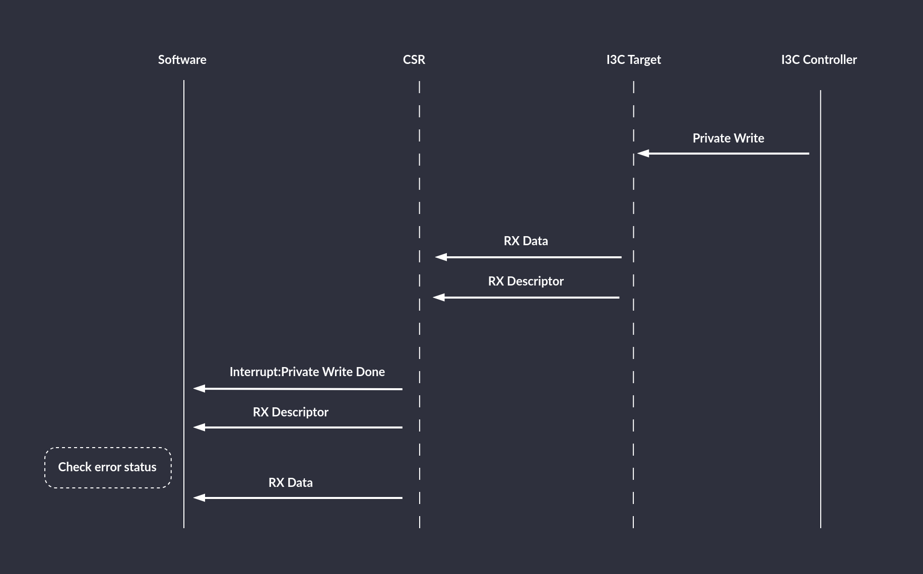
Figure 4 Private Write timing diagram
During the Private Write transaction, an error can be caused by:
bit flip, which will be detected by the parity bit
lack of space in the RX queue (overrun)
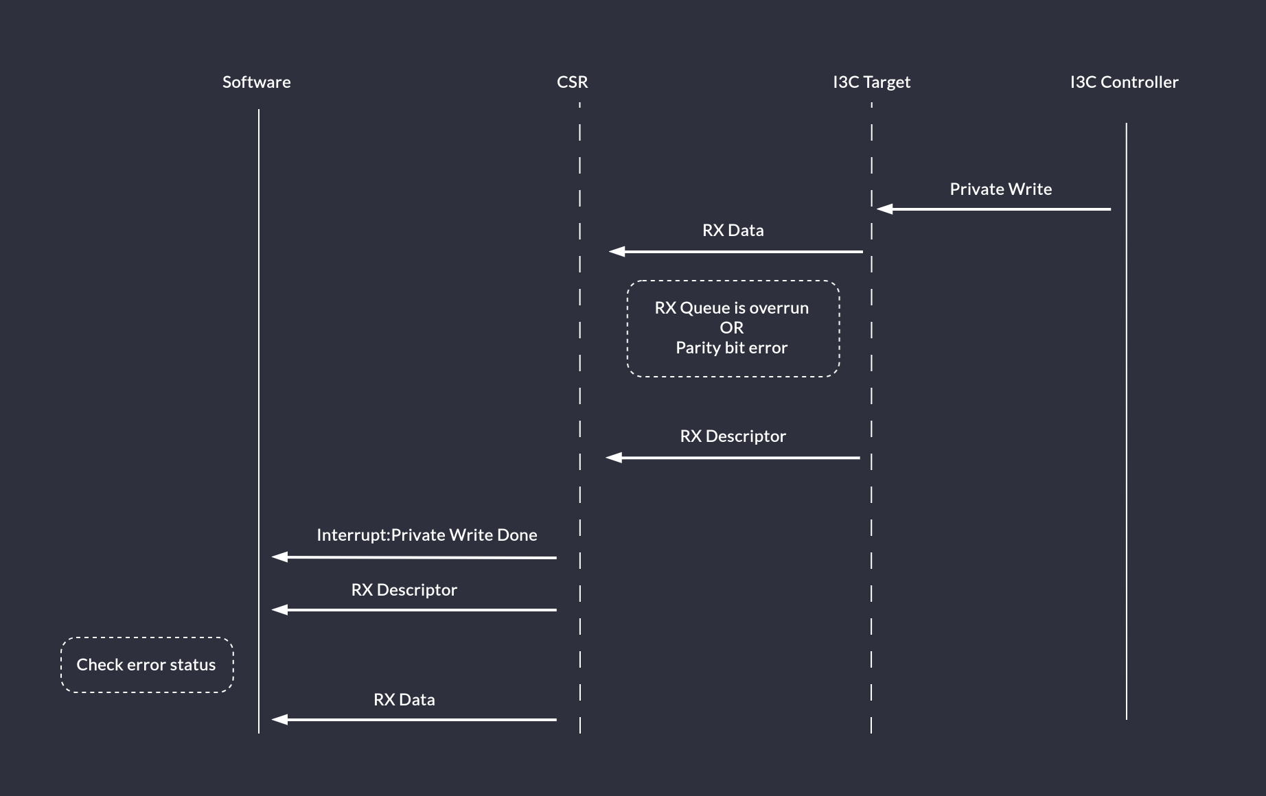
Figure 5 Private Write timing diagram: Parity bit error or RX Queue overrun scenario
If an Controller writes more data to the Target Device than it is capable to handle (even with triggering interrupts on threshold), the generated TTI RX Descriptor will indicate an error status and the Target Device should not ACK data on the bus.
The Controller can attempt mitigating such a situation by reading Target queue size from the TTI_QUEUE_SIZE register before sending a big chunk of data.
In-Band Interrupts
The Controller expects to receive an IBI Status Descriptor which is then followed by consecutive DWORDs of IBI Data.
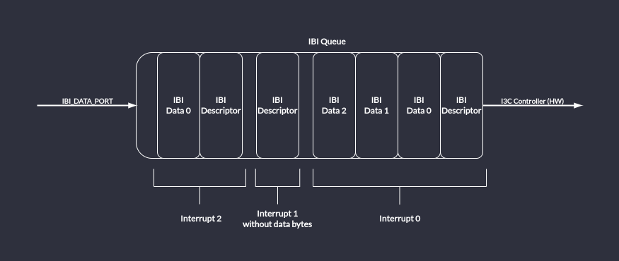
Figure 6 IBI Queue: partially filled with 3 interrupts.
In order to request an IBI, first the software should read the IBI queue size and set the queue threshold accordingly. Next, the interrupts should be enabled and an IBI descriptor with data can be written to the IBI_DATA_PORT. If, at this time, the IBI_THLD_STAT bit is set, then software should not attempt to write another IBI Descriptor into the queue. Software should wait until the IBI_THLD_STAT is cleared by hardware. The Target device will not try to send the IBI onto the I3C Bus until the bus is in the Available state. Also, it will read the IBI descriptor and wait until the IBI queue has all required data entries*. After meeting these conditions, the IBI will be driven onto the bus. The Target device will raise the IBI_DONE interrupt to notify that the IBI is finished. The software should read the LAST_IBI_STATUS to determine if the IBI ended successfully or was rejected. In case of failure, if the data integrity was not violated, the IBI will be retried once automatically.
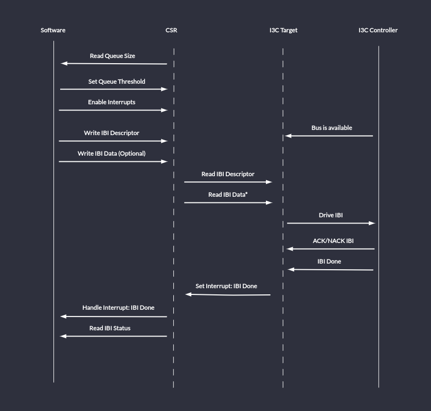
Figure 7 IBI Timing Diagram: send an IBI.
Register Interface
For a detailed list of TTI registers, refer to the TTI Registers chapter.
Data Structures (descriptors)
The TX Descriptor is 32-bit wide and has the following format:
Field Name |
Position (Size [bits]) |
Description |
DATA_LENGTH |
[15:0] (16) |
Number of data bytes in the TX Transaction. |
The RX Descriptor is 32-bit wide and has the following format:
Field Name |
Position (Size [bits]) |
Description |
ERROR |
[31:28] (4) |
Error occurred during this transaction. Software should read and discard data from the RX Queue. Values: 0x0: Success 0x1: Generic error 0x2-0xF: Reserved, will be used to determine type of error. |
DATA_LENGTH |
[15:0] (16) |
Number of data bytes in the RX Transaction. |
The IBI Descriptor is 32-bit wide and has the following format:
Field Name |
Position (Size [bits]) |
Description |
MDB |
[31:24] (8) |
Mandatory Data Byte. This field is valid if BCR[2] is set. |
DATA_LENGTH |
[7:0] (8) |
Number of data bytes in the IBI. |
TTI Queues
TTI TX Descriptor, TTI TX Data, TTI RX Descriptor, TTI RX Data and TTI IBI queues are implemented as FIFO queues of 32 bit (1 DWORD) width.
Depth should be parametrizable and the TTI_QUEUE_SIZE register’s reset value should be set accordingly.
In order to prevent overflow/underrun scenarios, a programmable threshold signal is provided.
Software-issued reset of the queues contents is also possible.