8fed18c
![]()
Caliptra: A Datacenter System on a Chip (SoC) Root of Trust (RoT)
Revision 2.1
Version 0.1
Introduction
Caliptra1 was originally created as part of the Open Compute Project (OCP). The major revisions of the Caliptra specifications are published at OCP. The evolving source code and documentation for Caliptra are in this repository within the CHIPS Alliance Project, a Series of LF Projects, LLC.
The objective of Caliptra is to define core RoT capabilities that must be implemented in the System on Chip (SoC) or ASIC of any device in a cloud platform. The collection of these RoT capabilities is referred to as the Silicon RoT Services (Silicon RoT).
Background
The overall security posture of silicon devices depends on establishing a core root of trust (RoT) and chain of trust. The core root of trust and chain of trust must attest to the integrity of configuration and mutable code.
Traditional RoT architectures offer many intrinsic security services and hosted security applications on a trusted execution environment (TEE). These architectures include (but are not limited to) hardware capabilities (cryptographic and microprocessor), ROM, firmware, and API infrastructure. These solutions are instantiated in discrete or integrated forms in various platform and component architectures.
Some of these solutions are either proprietary or aligned to specific parts of industry standards, consortium, or association specifications; for example, National Institutes of Standards and Technology (NIST), Open Compute Project (OCP), Trusted Computing Group (TCG), Distributed Management Task Force (DMTF), Institute of Electrical and Electronics Engineers (IEEE), etc. These solutions may be certified to conform to various standards; for example, the NIST cryptographic algorithm Validation program (CAVP).
Establishing a consistent RoT on very different hardware configurations while maintaining configuration and deployment flexibility is challenging. There is no uniform configuration across Cloud Service Providers (CSPs). For example, a system with host processors has very different firmware security measures when compared to a system without head-nodes or host processors.
The OCP Security WG specifications are making progress toward establishing the platform and peripheral security architecture recommendations that are necessary to attain the desired consistency in platform security orchestration.
Silicon RoT goals
To drive agility of specification definition and to maximize applicability, the scope of Caliptra is deliberately minimalistic. This minimalist approach drives industry alignment, consistency, and faster adoption of foundational device security primitives. A well and narrowly defined specification maximizes architectural composability; reusability across CSPs, products, and vendors; and feasibility of open sourcing.
Enhancements and advanced use cases and applications are outside the scope of this specification and may be developed in the form of a roadmap for the Silicon RoT and community engagement.
Caliptra 2.0 defines a design standard for a Silicon internal RoT baseline. This standard satisfies a Root of Trust for Measurement (RTM) and cryptographic services for the SoC. The SoC must measure the code and configuration it boots into Caliptra in this configuration. Caliptra must store these measurements and report them with signed attestations rooted in unique per-asset cryptographic entropy. As such, Caliptra serves as a Root of Trust for Identity (RTI) for the SoC.
The Caliptra Subsystem further standardizes SoC protection mechanisms with Root of Trust for Update (RTU) and Root of Trust for Recovery (RTRec). The open-source implementation of Caliptra drives transparency and consistency into the root of trust mechanisms that anchor foundational security services for the SoC.
Within this scope, the goals for a Caliptra 2.0 specification with subsystem include:
- Definition and design of the standard silicon internal RoT baseline:
- Reference functional specification:
- Scope including RTM, RTU and RTRec capabilities
- Control over SoC non-volatile state, including per asset entropy
- Reference APIs:
- Attestation APIs
- Authentication APIs
- Recovery APIs
- Internal SoC Cryptographic services
- Reference implementation
- Open source reference (including RTL and firmware reference code):
- For implementation consistency, using open source dynamics to avoid pitfalls and common mistakes
- For accelerated adoption, so that future products can leverage existing designs and avoid having to start the design process from scratch
- For greater transparency, to avoid fragmentation in the implementation space
- Firmware and RTL logical design are open, managed by consortium
- Reference functional specification:
- Consistency - across the industry in the internal RoT (iRoT) architecture and implementation:
- DICE identity, measurement, and recovery
- The silicon iRoT scope includes all datacenter-focused server class SoC / ASIC (datacenter focused) devices (SSD - DC, NIC, CPU, GPU - DC):
- Critical priority are devices with the ability to handle user plain text data
- Top priority are CPU SoCs
- Other examples include SmartNIC and accelerators
- 2.0 scope includes further datacenter devices such as
- SSD, HDD, BMC, DIMM, PSU, CPLD etc.
- Critical priority are devices with the ability to handle user plain text data
Note that Caliptra reference code (including RTL and firmware) is intended to be adopted as-is, without modification.
Explicitly out of scope is how silicon integration into backend work is performed such as:
- Foundry IP integration
- Physical design countermeasures
- Analog IPs
- Post manufacture test and initialization (OSAT)
- Certification
Use cases
The Silicon RoT use cases can be supported through the adoption of specific industry standards, and association and consortium specifications. For more information, see specific documents in References.
In this version of the specification, the desired capabilities address the basics of supply chain security use cases.
Supply chain security
- Mutable code integrity: The objective is to prove the device is running genuine firmware such that the device manufacturer can vouch for its authenticity and integrity, and the device owner can ensure only authorized updates are applied to the device. This flow is aligned with Reference 9 and can be achieved with dual signature verification of equal imposition.
- Configuration and lifecycle management: The objective is to allow the platform owner to securely configure the RoT capabilities, and to enable and authorize lifecycle state transitions of the SoC.
DICE Protection Environment
Caliptra implements the DICE Protection Environment (DPE) API, allowing it to derive and wield a DICE identity on behalf of other elements within the SoC. Use cases for this API include serving as a signing oracle for a Security Protocol and Data Model (SPDM) responder that is executing in a SoC application processor (in passive mode) or in the Manufacturer Control Unit (MCU in subsystem mode), as well as authentication to a discrete TPM device.
Industry standards and specifications
This specification follows the industry standards and specifications listed in References.
NIST SP 800-193 Platform Firmware Resiliency
Per Reference 1, RoT subsystems are required to fulfill three principles: protection, detection and recovery. The associated RoT services are referred to as:
- The Root of Trust for Update (RTU) is responsible for authenticating firmware updates and critical data changes to support platform protection capabilities.
- The Root of Trust for Detection (RTD) is responsible for firmware and critical data corruption detection capabilities.
- The Root of Trust for Recovery (RTRec) is responsible for recovery of firmware and critical data when corruption is detected, or when instructed by an administrator.
These RoT services can be hosted by a complex RoT as a whole or these services can be spread across one or more components within a platform. This determination has a basis in physical risk. Physical adversaries with reasonable skill can bypass a discrete RoT’s detection capabilities, for example, with SPI interposers.
However, a RoT embedded within a SoC or ASIC represents a much higher detection bar for a physical adversary to defeat. For this reason in Caliptra 2.0 Core, the cryptographic module shall deliver the Detection capability for itself while providing Measurement and Identity services for the rest of the SoC. The Measurement and Identity services that Caliptra provides can be used by the SoC to create Detection capability for the measured firmware and configuration data.
The objectives of Caliptra Core are minimalistic scope and maximum applicability. To that end, Update and Recovery are decoupled from Caliptra Core and are expected to be provided either by Caliptra 2.0 Subsystem or are expected to be provided by an external RoT subsystem, such as a discrete RoT board element on a datacenter platform (passive mode). Because a physical adversary can trivially nullify any recovery or update capabilities, no matter where implemented, decoupling represents no regression in a security posture, while enabling simplicity and applicability for the internal SoC Silicon RoT.
Detection of corrupted critical code and data (configuration) requires strong end to end cryptographic integrity verification. To meet the RTD requirements, Silicon RoT shall:
- Cryptographically verify & measure its code and configuration
- Sign these measurements with a unique attestation key
- Report measurements to a host or external entity, which can further verify the authenticity and integrity of the device (also known as attestation)
- Recovery follows Open Compute Project Secure Recovery flows and Streaming Boot. (FIXME: Add links to released specs; they are in draft mode now)
Measurements and Verification include Code and Configuration. Configuration includes invasive capabilities that impact the user service level agreement (SLA) on confidentiality; for example, the enablement of debug capabilities that grant an operator access to raw, unencrypted registers for any tenant context. In order to measure and attest configuration, the Silicon RoT must be in control of the configuration.
As an extension to controlling configuration, the Silicon RoT must control the security states (for more information, see Caliptra Security States). Certain security states by design grant full invasive capabilities to an external operator, for debug or field analysis.
Measurements must be uniquely bound to the device and its manufacturer at a minimum. This establishes the need for Identity services in the Silicon RoT, which serve as the basis for key derivation and attestation authenticity.
For further details about how Caliptra addresses NIST SP 800-193, see Device Resilience.
Trusted Computing Group (TCG) DICE Attestation
In accordance with OCP Attestation specification Reference 8, devices must have a cryptographic identity for the endorsement of attestation quotes. The RTM implementation follows TCG DICE (for information, see Reference 4, Reference 5, and Reference 6). One of the benefits of TCG DICE device identities is having renewable security. This renewability complements ownership transfer and circular economy. The new owner is not burdened with the identity of the previous owner, nor is the new owner burdened with trusting an irrevocable hardware identity certificate. This benefits the transferee, as their identities can be revoked through standard PKI mechanisms. DICE based certificates are fully compatible with Public Key Infrastructure (PKI), including full lifecycle management and PKI Certificate Revocation List (CRL).
Operational security during the manufacturing process is critical, to ensure the DICE entropy is securely initialized, certified, and registered. Operational security avoids any pilfering of this asset by eavesdroppers. Operational security is outside the scope of this specification.
Threat model
The Caliptra threat model describes attacker profiles, assets and attack surfaces, and paths to these assets based on attacker profiles. Subsections provide further details.
Threat scenarios as comprehended by assets and possible attack paths are as complete as possible but focus on the worst case scenarios. Thus not every attack path to asset is captured in this threat model.
Attacker profiles
An attacker profile is based on factors like the tools that are accessible to the attacker, the level of access to the target of evaluation, and expertise of the attacker to use these methods. These factors are described in the following tables.
Table 1: Tools accessible to attacker
| Attack tools | Type of attack | Purpose and usage |
|---|---|---|
| Debuggers, fuzzing devices, image reverse engineering tools, and software payloads | Logical fault injection | Find logical and functional vulnerabilities and exploit those to achieve unauthorized operations. |
| Clock fault injectors, voltage fault injectors, electromagnetic fault injectors, optical fault injectors, and micro probing | Environmental fault injection | Alter the execution flow of the critical decision points, especially in the early execution. |
| Power analyzers, timing analyzers (scopes, etc.), low speed bus analyzers, and optical emission analyzers | Side channel analysis | Infer security sensitive information by analyzing various operational conditions. |
| Microscopic imaging, reverse engineering, scanning electron microscope imaging, and focused ion beam (FIB) | Chip invasive attacks | Decapsulation, depackaging, and rebonding to probe the internals of the chip. |
Table 2: Type of access to level of access
| Type of access | Levels of access | Attack paths available |
|---|---|---|
| Physical access | Unrestricted access for physical and logical attacks. | Chip invasive attacks and chip non-invasive attacks |
| Remote access | Limited access for attacks with both privileged and unprivileged access rights. | Chip non-invasive attacks and network attacks |
Table 3: Definition of expertise (JIL)
| Proficiency level | Definition | Detailed definition |
|---|---|---|
| Expert | Can use chip invasive, fault injections, side channels, and logical tools. Understands hardware and software in depth. Familiar with implementation: - Algorithms - Protocols - Hardware structures - Principle and security concepts | Developer-level knowledge of algorithms, protocols, hardware structure, and principles. Understands techniques and tools for attacks. |
| Proficient | Can use fault injections, side channels, and logical tools. Has reasonable understanding of hardware and software. Familiar with security behavior. | Familiar with security behavior and classical attacks. |
| Layperson | No particular expertise. | No particular expertise. |
Types of attacks
Physical attacks
A physical attacker has full access to the electrical and physical components. This includes access to interfaces, connectors, and ports of the SoC/ASIC in which Caliptra is integrated without restriction.
Invasive attacks that involve depackaging or delayering of the SoC/ASIC are out-of-scope. Non-invasive attacks are in scope.
- Fault injection attacks
- Counter measurements - as strong recommendation
- Power and electromagnetic analysis attacks
- Counter measurements - as strong recommendation
Table 4: Attack types
| Attack | Description | Threat model scope |
|---|---|---|
| Electromagnetic – passive | Attacker observes the electromagnetic power spectrum and signals radiated from the product. | - Includes all attacks at all frequency ranges, including radio frequencies, infrared, optical, and ultraviolet. - Excludes attacks that require removing the package lid. |
| Electromagnetic – active | Attacker directs electromagnetic radiation at the product or portions of the product. | - Includes all attacks at all frequency ranges, including radio frequencies, infrared, optical, and ultraviolet. - Excludes attacks that require removing the package lid. |
| Electric – passive | Attacker probes the external pins of the package and observes electrical signals and characteristics including capacitance, current, and voltage signal. | - Includes both analog attacks and digital signal attacks. - Excludes attacks that require removing the package lid. |
| Electric – active | Attacker alters the electrical signal or characteristics of external pins. | - Includes both analog attacks and digital signal attacks. - Excludes attacks that require removing the package lid. |
| Temperature – passive | Attacker observes the temperature of the product or portions of the product. | Excludes attacks that require removing the package lid. |
| Temperature – active | Attacker applies external heat sources or sinks to alter the temperature of the product, possibly in a rapid fashion. | - Includes all temperature ranges (for example, pouring liquid nitrogen over the package or heating the package to above 100 C). - Excludes attacks that require removing the package lid. |
| Sound - passive | Attacker observes the sounds emitted by the product. | - Includes all frequencies. - Excludes attacks that require removing the package lid. |
Table 5: Logical attacks
| Attack | Description | Threat model scope |
|---|---|---|
| Debug and register interfaces | Manipulation of externally accessible registers of Caliptra. | Includes all buses that are accessible to components external to Caliptra, including JTAG. |
| Software interfaces | Attacker invokes software interfaces that are exposed by Caliptra to external components. | Includes all externally exposed software interfaces from both non-RoT firmware as well as interfaces accessed by external IP blocks. Includes exploiting both design and implementation flaws. For high value assets only (see next subsection), the attacker is assumed to fully control all mutable code of the SoC, including privileged Caliptra mutable code. |
| Side channel - timing | Attacker observes the elapsed time of different sensitive operations. | Includes attacks where the attacker actively stimulates the sensitive operations while timing. |
| Cryptographic analysis | Attacker observes plaintext, ciphertext, related data, or immediate values in cryptography to overcome cryptographic controls. | Includes all practical cryptanalysis attacks. Assumes NIST-unapproved algorithms provide no security (for example, SHA-1, Single DES, ChaCha20). Assumes any cryptographic algorithm that provides less than 128 bits of security (as determined by NIST SP 800-57) provides no security. |
Trust boundaries
The following figure shows trust boundaries for the discussion of threat modeling. SoCs based on Caliptra are expected to have Caliptra as silicon RoT, and are expected to have a platform or SoC security engine to orchestrate SoC security needs for the rest of the SoC.
Trust levels of Caliptra and the SoC security engine are not hierarchical. These two entities are responsible for different security aspects of the chip.
Figure 1: Caliptra trust boundaries
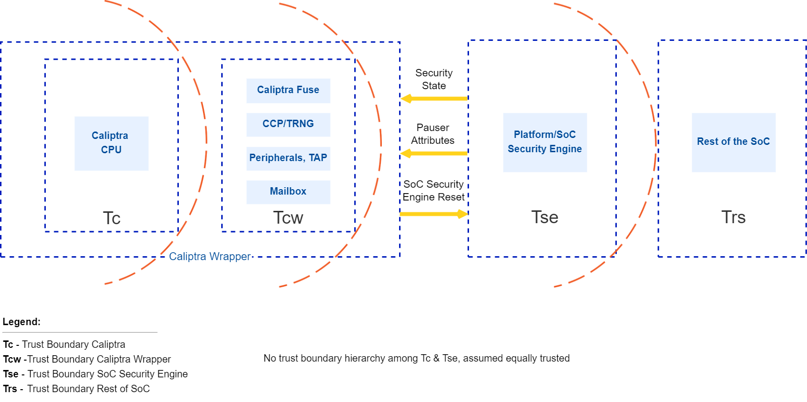
Caliptra interactions
The Caliptra Core blocks consume the Tc and Tcw trust level components. This boundary includes crypto accelerators, hardware key sequencer, key vault, Caliptra microcontroller, ROM, and subsystem interconnects. The Caliptra Core provides deterministic Caliptra behavior. Caliptra Core interacts with components in the Tse and Trs trust levels; while Caliptra Subsystem abosrbs the Tse functions.
Caliptra assets and threats
Assets are defined to be secrets or abilities that must be protected by an owner or user of the asset. Ownership means that the owner has the responsibility to protect these assets and must only make them available based on a defined mechanism while protecting all other assets.
An example of when an owner must protect assets is moving from secure mode to insecure mode. Another example is moving from one owner to another. Before moving through these transitions, the owner must ensure all assets are removed, disabled, or protected based on how the use case is defined.
Table 6: Assets
| Asset category | Asset | Security property | Attack profile | Attack path | Mitigation |
|---|---|---|---|---|---|
| Fuse/OTP high value secrets | UDS Seed | Confidentiality and integrity | Expert | Malicious manufacturing spoofing of UDS Seeds | UDS obfuscation with class RTL key |
| Fuse/OTP high value secrets | UDS Seed | Confidentiality and integrity | Expert | Invasive attack (fuse analysis) | Shield fuse IP |
| Fuse/OTP high value secrets | UDS Seed | Confidentiality and integrity | Expert | Boot path tampering while retrieving UDS values | UDS obfuscation with class RTL key |
| Fuse/OTP high value secrets | UDS Seed | Confidentiality and integrity | Expert | Attempting to derive die specific keys by knowing UDS | Confine unobfuscated UDS and subsequent derivations to key vault |
| Fuse/OTP high value secrets | Field entropy | Confidentiality and integrity | Expert | Malicious manufacturing spoofing on field entropy | Field entropy obfuscation with class RTL key |
| Fuse/OTP high value secrets | Field entropy | Confidentiality and integrity | Expert | Invasive attack (fuse analysis) | Shield fuse IP |
| Fuse/OTP high value secrets | Field entropy | Confidentiality and integrity | Expert | Boot path tampering while retrieving field entropy values | Field entropy obfuscation with class RTL key |
| Fuse/OTP high value secrets | Field entropy | Confidentiality and integrity | Expert | Attempting to derive die specific keys by knowing field entropy | Confine unobfuscated field entropy and subsequent derivations to key vault |
| Fuse/OTP high value secrets | FW authentication keys | Integrity | Proficient | Glitching | 1. Redundant decision making on critical code execution 2. Error check before consuming values from fuses 3. Environmental monitoring and protection |
| Fuse/OTP high value secrets | Versioning information from fuses | Integrity | Proficient | Glitching | Environmental monitoring and protection |
| Fuse/OTP high value secrets | IDEVID CERT chain | Integrity | Proficient | Glitching | 1. Environmental monitoring and protection 2. Error check before consuming values from fuse in various ways |
| Fuse/OTP high value secrets | OCP L.O.C.K. HEK RATCHET SEED | Confidentiality | Proficient | 1. Glitching 2. Software writing to modify the valid seed | 1. Consuming it after obfuscating with class RTL key 2. Environmental monitoring and protection 3. Error check before consuming values from fuse in various ways |
| Die unique assets | UDS (802.1AR Unique Device Secret) | Confidentiality and integrity | Proficient | 1. Software reading actual secrets 2. Side channel attack to infer secret | 1. Secrets locked in key vault, not readable by software 2. SCA protections |
| Die unique assets | CDIn (DICE compound device identifier for Layer n) | Confidentiality and integrity | Proficient | 1. Software reading actual secrets 2. Side channel attack to infer secret | 1. Secrets locked in key vault, not readable by software 2. SCA protections |
| Die unique assets | IDevIDPriv | Confidentiality and integrity | Proficient | 1. Software reading actual secrets 2. Side channel attack to infer secret | 1. Secrets locked in key vault, not readable by software 2. SCA protections |
| Die unique assets | LDevIDPriv | Confidentiality and integrity | Proficient | 1. Software reading actual secrets 2. Side channel attack to infer secret | 1. Secrets locked in key vault, not readable by software 2. SCA protections |
| Die unique assets | Obfuscation key | Confidentiality and integrity | Proficient | 1. Software reading actual secrets 2. Side channel attack to infer secret | 1. Secrets locked in key vault, not readable by software 2. SCA protections |
| Die unique assets | AliasFMC_KeyPriv | Confidentiality and integrity | Proficient | 1. Software reading actual secrets 2. Side channel attack to infer secret | 1. Secrets locked in key vault, not readable by software 2. SCA protections |
| Die unique assets | AliasRT_KeyPriv | Confidentiality and integrity | Proficient | 1. Software reading actual secrets 2. Side channel attack to infer secret | 1. Secrets locked in key vault, not readable by software 2. SCA protections |
| Root of trust execution | ROM FW | Integrity | Proficient | Glitching | 1. Redundant decision making on critical code execution 2. Environmental monitoring and protection |
| Root of trust execution | Execution unauthorized runtime FW | Authenticity and integrity | Proficient | Modify boot media | Authenticity and integrity check using PKI DSA upon power on |
| Root of trust execution | Execution unauthorized runtime FW | Authenticity and integrity | Proficient | Arbitrary payload pushed into execution | Authenticity and integrity check using PKI DSA during software updates and power on |
| Root of trust execution | Rollback Attack | Versioning | Proficient | 1. Modify boot media to host older versions 2. Bypass version check during boot | 1. Authenticity and integrity check using PKI DSA upon power on 2. Failproof, audited boot code implementation responsible for loading images |
| Root of trust execution | Control flow | Integrity and confidentiality if applicable | Proficient | 1. Return and jump addresses manipulation 2. Return values and errors tampering 3. Stack overflow 4. Buffer overflows 5. Privilege escalations and hijacking | 1. Various control flow integrity measures 2. Secure coding practices and auditing implementation |
| Boot measurements protected by Caliptra | Boot measurements that Caliptra gathers, stores, and reports | Integrity | Expert | 1. Manipulate measurements AiTM while in transit to Caliptra 2. SoC sends manipulated measurements to Caliptra | |
| Caliptra inputs | Security state | Integrity | Proficient | Glitching | Environmental monitoring and protection |
| Caliptra inputs | Mode selection (Boot Media Integrated and dependent selections) | Integrity | Proficient | Glitching | Environmental monitoring and protection |
| Caliptra inputs | AXI_USER attribute | Integrity | Proficient | Glitching | Environmental monitoring and protection |
| Caliptra inputs | Design-for-Test (DFT) and Design-for-Debug (DFD) | Integrity | Proficient | 1. Attempt to manipulate RoT execution via DFT or DFD flows to flows that are not plan-of-record 2. Attempt to retrieve device secrets via DFT or DFD flows when product is field-deployed 3. Attempt to retrieve device secrets via DFT or DFD flows while the product is being developed and debugged | Implement scan mode and debug unlock management within Caliptra with the required SoC support |
High level architecture
The following figure shows the basic high-level blocks of Caliptra.
Figure 2: Caliptra high level blocks
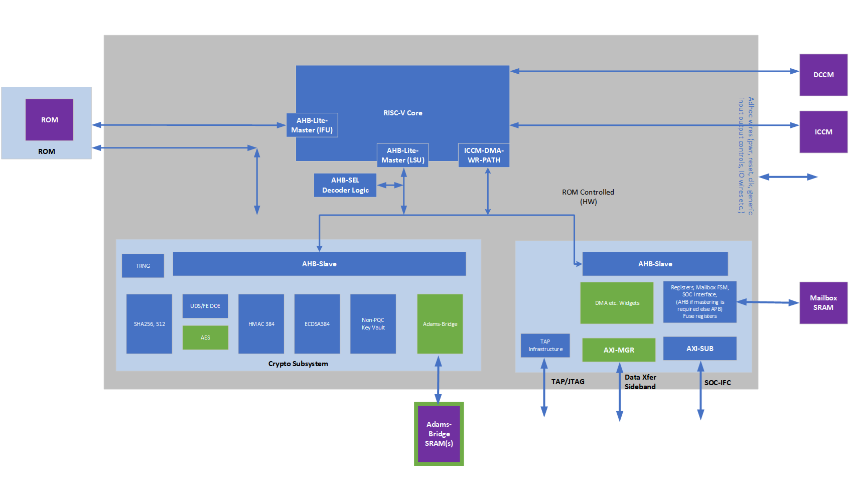
See the hardware section for a detailed discussion.
From Caliptra 2.x onwards, Caliptra introduces three integration variants: Passive mode (supported in the 1.x architecture), Subsystem mode, and Caliptra Subsystem w/ OCP L.O.C.K.
- Passive Mode: Caliptra coordinates the start of the firmware chain-of-trust with the SoC, but the SoC manages its own update and recovery.
- Subsystem Mode: Caliptra is the RoT for the SoC and provides streaming boot, secure boot, attestation, and various cryptographic API services (such as encryption/decryption of SoC FWs, key releases, key wraps, and hashing).
- Caliptra Subsystem w/ OCP L.O.C.K: This variant extends the Caliptra Subsystem to include OCP L.O.C.K features. In this variant, Caliptra acts as a Key Management Block (KMB), providing secure key management, media encryption key (MEK) protection, and programming into the storage device's encryption engine via a dedicated hardware interface, ensuring that the MEK is never visible to mutable firmware.
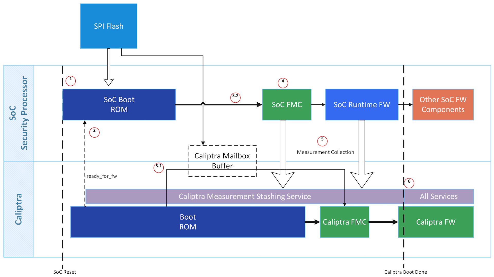
Passive Mode High Level Flow
Caliptra is among the first microcontrollers taken out of reset by the power-on reset logic. Caliptra coordinates the start of the firmware chain-of-trust with the immutable component of the SoC ROM. After the Caliptra ROM completes initialization, it provides a "stash measurement" API and callback signals for the SoC ROM (passive mode) to proceed with the boot process. Caliptra ROM supports stashing of at most eight measurements prior to the boot of Caliptra RT firmware. The SoC then may choose to boot Caliptra firmware. Any security-sensitive code or configuration loaded by the SoC prior to Caliptra firmware boot must be stashed within Caliptra. If the SoC exceeds Caliptra ROM's measurement stash capacity, attestation must be disabled until the next cold reset. The boot process is as follows:
- Hardware executes SoC power-on reset logic. This logic starts the execution of SoC ROM and Caliptra ROM.
- SoC ROM waits for the ready_for_fw signal from Caliptra ROM.
- SoC ROM fetches the FMC.
- If the FMC is Caliptra firmware:
- SoC ROM loads the Caliptra firmware into the Caliptra mailbox and issues the Caliptra "firmware load" command.
- Caliptra ROM authenticates, measures, and starts the Caliptra firmware.
- If the FMC is not Caliptra firmware:
- SoC ROM measures that firmware as the SoC FMC, and issues the Caliptra "stash measurement" command prior to executing SoC FMC.
- If the FMC is Caliptra firmware:
- SoC ROM executes SoC FMC.
- SoC FMC continues the boot process, forming a boot firmware chain-of-trust: each firmware fetches, authenticates, measures, and executes the next firmware needed to establish the device operating environment. Each firmware deposits the next firmware's measurements into Caliptra prior to execution. The exception is Caliptra's firmware: SoC firmware delegates the measurement and execution of Caliptra's firmware to Caliptra ROM.
- Upon eventual initialization, Caliptra firmware presents attestation APIs using the deposited measurements.
See Error Reporting and Handling for details about Caliptra and SoC firmware load and verification error handling.
Figure 3: Passive Caliptra boot flow
Subsystem Mode Boot Flow
MCU (Manufacturer Control Unit), that is holds platform & SoC specific FW and Caliptra are among the first microcontrollers taken out of reset by the power-on reset logic. Caliptra is responsible for the start of the firmware chain-of-trust with the immutable component of the MCU ROM. After the Caliptra ROM completes initialization, it provides a "stash measurement" API and callback signals for MCU ROM (subsystem mode) to proceed with the boot process. Caliptra ROM supports stashing of at most eight measurements prior to the boot of Caliptra RT firmware. Then Caliptra FW is loaded through OCP streaming boot flow. The OCP streaming boot flow uses an I3C controller with commands defined by the OCP Recovery specification. This controller constitutes the streaming boot interface in the boot flow below. Any security-sensitive code (eg. PLL programming) or configuration (eg. Fuse based Patching) loaded by the MCU prior to Caliptra firmware boot must be stashed within Caliptra. If the MCU exceeds Caliptra ROM's measurement stash capacity, attestation must be disabled until the next cold reset.
Note: This is extremely high level flow, please see the Subsystem Mode Section below for next level specifics.
The high level boot process is as follows:
- Hardware executes SoC power-on reset logic. This logic starts the execution of MCU ROM and Caliptra ROM.
- Streaming boot interface is gated until ready for recovery is written into streaming boot interface registers from Caliptra ROM. This happens at the same time as passive mode's ready_for_fw signal.
- Caliptra firmware is streamed & then pulled into Caliptra MB SRAM through the OCP streaming boot interface by a platform component (typically a BMC-like component). 1. Caliptra ROM authenticates, measures, and activates the Caliptra firmware.
- SoC manifest is streamed next via the streaming boot interface, which Caliptra authenticates & measures
- This is followed by MCU RT FW through the streaming boot protocol which Caliptra routes to MCU SRAM, authorizes and activates MCU to execute it.
- MCU RT FW will go through MCTP enumeration and fetch the remaining SoC blobs (FW, data etc.) using DSP0267 PLDM for Firmware Update over MCTP and uses Caliptra to authorize each of them. Note that MCU may also retrieve some non-FW blobs from a NVM while using Caliptra to perform security operations like integrity verification, decryption etc.
FIXME: ADD a pic
Identity
Caliptra must provide its runtime (RT) code with a cryptographic identity in accordance with the TCG DICE specification. This identity must be rooted in ROM, and provides an attestation over the security state of the RTM as well as the code that the RTM booted.
To ensure quantum-resistant RTM, each certificate includes a dual signatures based on ECC Secp384r1 and PQC MLDSA-87.
Figure 4: DICE Cert/Key generation

UDS
A combination of mask ROM and HW macros must implement the DICE key derivation and power-on latch, hiding the UDS seed and only making the CDI-derived signing key 'handle' visible to ROM. Real UDS will only be calculated during the cold boot in hardware, used for CDI derivation and immediately gets cleared.
The Caliptra UDS seed is stored as ciphertext in fuses, deobfuscated only on cold boot using a obfuscation key2 known only to the Caliptra Hardware. Once read by Caliptra HW at boot, the unobfuscated UDS is then used to derive the IDevID identity and immediately cleared by hardware.
IDevID key
Caliptra's IDevID key is a hardware identity generated by Caliptra ROM during manufacturing. This key "handle" must be solely wielded by Caliptra ROM, and shall never be exposed externally at any phase of the Caliptra lifecycle. IDevID is used to endorse LDevID. Caliptra supports both classic and post-quantum algorithms for endorsement based on ECDSA Secp384r1 and PQC MLDSA-87, respectively. The IDevID certificate is endorsed by the vendor’s provisioning CA (pCA) that is implemented via a HSM appliance connected to High Volume Manufacturing (HVM) flows (see provisioning CA in Reference 8).
See Provisioning IDevID During Manufacturing for further details on IDevID provisioning.
LDevID key
Caliptra shall support field-programmable entropy, which factors into the device's LDevID identity. The LDevID certificate is endorsed by IDevID and in turn endorses the FMC alias key. Caliptra supports both classic and post-quantum algorithms for endorsement based on ECDSA Secp384r1 and PQC MLDSA-87, respectively.
Caliptra's field-programmable entropy shall consist of two 16-byte slots. All slots are used to derive LDevID. An owner may decide to program as few or as many slots as they wish. Upon programming new entropy, on the next reset the device begins wielding its fresh LDevID. Owners need to validate the new LDevID by using IDevID.
Commentary: threat analysis
An ideal IDevID has the following properties:
- Cannot be altered by entities besides Caliptra in manufacturing security state.
- Cannot be impersonated by entities that are not a Caliptra instatiation for that device class.
- Cannot be cloned to additional devices of the same class.
- Private component cannot be extracted from Caliptra.
Caliptra 2.0 provides integrity over IDevID Certificate Signing Requests (CSRs).
Caliptra 1.0 alone does not fully address these properties. For example, a person-in-the-middle supply chain adversary could impersonate Caliptra by submitting its own IDevID CSR to the pCA. Vendors should threat model the IDevID generation and endorsement flows for their SoC. Threat actors to consider are the following:
- Components involved in UDS injection flows: can they inject the same obfuscated UDS to multiple devices, or to devices of different classes? Can they wield the obfuscation key to leak the UDS?
- Components servicing the connectivity between the Caliptra instantiation and the HSM applicance performing IDevID endorsement: can they alter or impersonate Caliptra's IDevID CSR?
- Physical attackers: see Physical Attack Countermeasures.
Vendors have incentives to mitigate these threats. The vendor identity chain secures RMA and confidential computing workflows.
Ultimately though, IDevID is not renewable. Renewable security, often referred to as trusted computing base recovery, is a base design principle in Caliptra. Therefore, it is a design goal to reduce the operational dependency on IDevID. Field entropy and LDevID satisfy this need.
Field entropy is a limited resource, consisting of only two 16-byte slots of one-time programmable fuses. It is not generally expected that a second-hand purchaser can program all or even any of these slots. Caliptra's DICE identity remains usable even after all field entropy slots are programmed, so this feature does not preclude a circular economy. Field entropy is a feature primarily designed for users who purchase new parts.
Field entropy and LDevID are intended to hedge against attackers with the following abilities:
- Can obtain UDS before the part first arrives at the owner's facility.
- Can wield that stolen UDS to impersonate the part after it is deployed within the owner's facility. The attacker can derive and wield IDevID to mint an attacker-controlled DICE hierarchy; for example, LDevID, FMC alias key, or Runtime firmware alias key.
- Cannot fully impersonate the part during initial onboarding within the owner's facility.
- Cannot extract field entropy after initial onboarding.
During initial onboarding, the owner is expected to instruct the device to program field entropy. Upon device reset, this results in a fresh LDevID. Attackers that have previously obtained UDS are not able to derive this LDevID. The owner is expected to register the new LDevID and subsequently validate all future DICE keys for the device against that LDevID.
When registering LDevID during device onboarding, the owner is expected to rely on IDevID as an authenticity signal over LDevID. It is assumed that the attacker has obtained UDS at this point, and therefore can themselves wield IDevID. Therefore, the authenticity signal granted by IDevID cannot be the only signal used to determine LDevID's trustworthiness. The owner's device onboarding flow must be resistant to remote person-in-the-middle attackers that may attempt to use a previously exfiltrated UDS to register a forged LDevID.
After an owner registers a device's LDevID as part of their device onboarding flow, and unless the device again passes through the owner's device onboarding flow, the owner should not trust IDevID to endorse any other LDevIDs.
This approach does not defend against supply-chain attackers that obtain fuse data for devices that enter the supply chain after their field entropy has been programmed, such as during RMA flows. The LDevID certificate also does not support revocation because there is no generic Caliptra OCSP service. Owners should either maintain an allowlist of LDevID certificates or revoke any of the upstream certificate authorities.
Owners are not required to program field entropy. Caliptra generates LDevID from the value of the field entropy fuses, which could be all zeroes or ones. Caliptra LDevID derivation descends from UDS so that LDevID properties are no worse than IDevID. Field entropy is expected to be stored in fuses to achieve an equivalent physical attack barrier to UDS.
It is the responsibility of the owner or the user to identify the certificate they wish to trust, and to potentially endorse with their own certificate authority: pCA, IDevID, LDevID, or AliasFMC.
FMC alias key
The LDevID CDI is mixed with a hash of FMC, as well as the security state of the device, via a FIPS-compliant HMAC, to produce CDIFMC. ROM uses CDIFMC to derive the AliasFMC keypair. ROM wields LDevID to issue a certificate for Alias. The AliasFMC certificate includes measurements of the security state and FMC. ROM makes CDIFMC, AliasFMC, and its certificate, available to FMC.
FMC mixes CDIFMC with a hash of runtime firmware to produce CDIRT. FMC uses CDIRT to derive the AliasRT alias keypair. FMC wields AliasFMC to issue a certificate for AliasRT. This alias certificate includes measurements of runtime firmware. FMC makes CDIRT, AliasRT, and its certificate, available to application firmware, while withholding CDIFMC and AliasFMC.
Security state
Devices may support features like debug unlock, DFT, or DFD flows that globally affect SoC state. These features, when enabled, significantly alter the security state of the device. The configuration of these features shall be captured in the device's DICE identity. The security state shall be captured as an input to the FMC's CDI, and represented within the FMC's alias certificate.
Owner authorization
Caliptra firmware shall be signed by the vendor. In addition, this firmware shall also be signed by an owner key. Caliptra must extract the owner's public key from the firmware image during cold boot, and latch the owner key into Caliptra's RAM for the remainder of its uptime3. Caliptra then uses both the vendor key and owner key to verify hitless firmware updates.
Caliptra shall attest to the value of the owner key, enabling external verifiers to ensure that the correct owner key was provisioned into the device. To perform this attestation, Caliptra includes the owner key as an input to the FMC's CDI (as part of "other attributes" from Figure 4 above), and represents it within the FMC's alias certificate.
The SoC may support a fuse bank for representing the hash of the owner's public key. If the SoC reports this value to Caliptra, Caliptra refuses to boot firmware unless the firmware was dual-signed by the key reported by SoC ROM's fuse registers.
The owner key, when represented in fuses or in the FMC's alias certificate, is a SHA384 hash of a structure that contains a list of owner public keys. This supports key rotation.
Provisioning UDS during Manufacturing (Subsystem Mode)
Note: In passive mode, SoC follows the same flows/restrictions as Caliptra 1.x
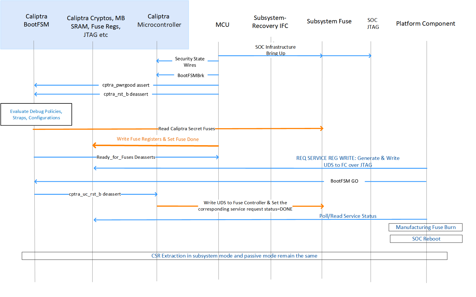
Figure 6: Subsystem Mode: UDS manufacturing flow
There are three ways of generating a UDS_SEED Use the internal TRNG to directly generate a 384-bit random number. Use an entity external to Caliptra such as an HSM or SoC-specific methodology to produce UDS-seed 384-bit random number that is pushed into the fuse controller (same as Caliptra 1.0). Combine the internal TRNG output with a Manufacturing time provided value to produce a 384-bit output.
UDS Manufacturing
- When SoC life cycle is in MANUFACTURING MODE, manufacturing service register bit [CPTRA_DBG_MANUF_SERVICE_REG[2]] is set to request for UDS seed programming flow.
- Caliptra ROM will sample this bit on power up; when this bit is set and Caliptra ROM rechecks that the life cycle state is manufacturing mode, it reads the iTRNG for a 512-bit value.
- Caliptra ROM writes the 512-bit value to the address available through a register named UDS_SEED_OFFSET which is strapped by SoC at integration time by using DMA HW assist macro available at ROM’s disposal.
- Caliptra ROM sets the corresponding status bit in CPTRA_DBG_MANUF_SERVICE_REG to indicate the flow completion.
- Manufacturing flow will poll/read this bit and then do the fuse burning flow as specified by the fuse controller spec and SoC specific VR methodologies (eg. Fuse macro voltage elevation flows etc.).
Provisioning IDevID during manufacturing
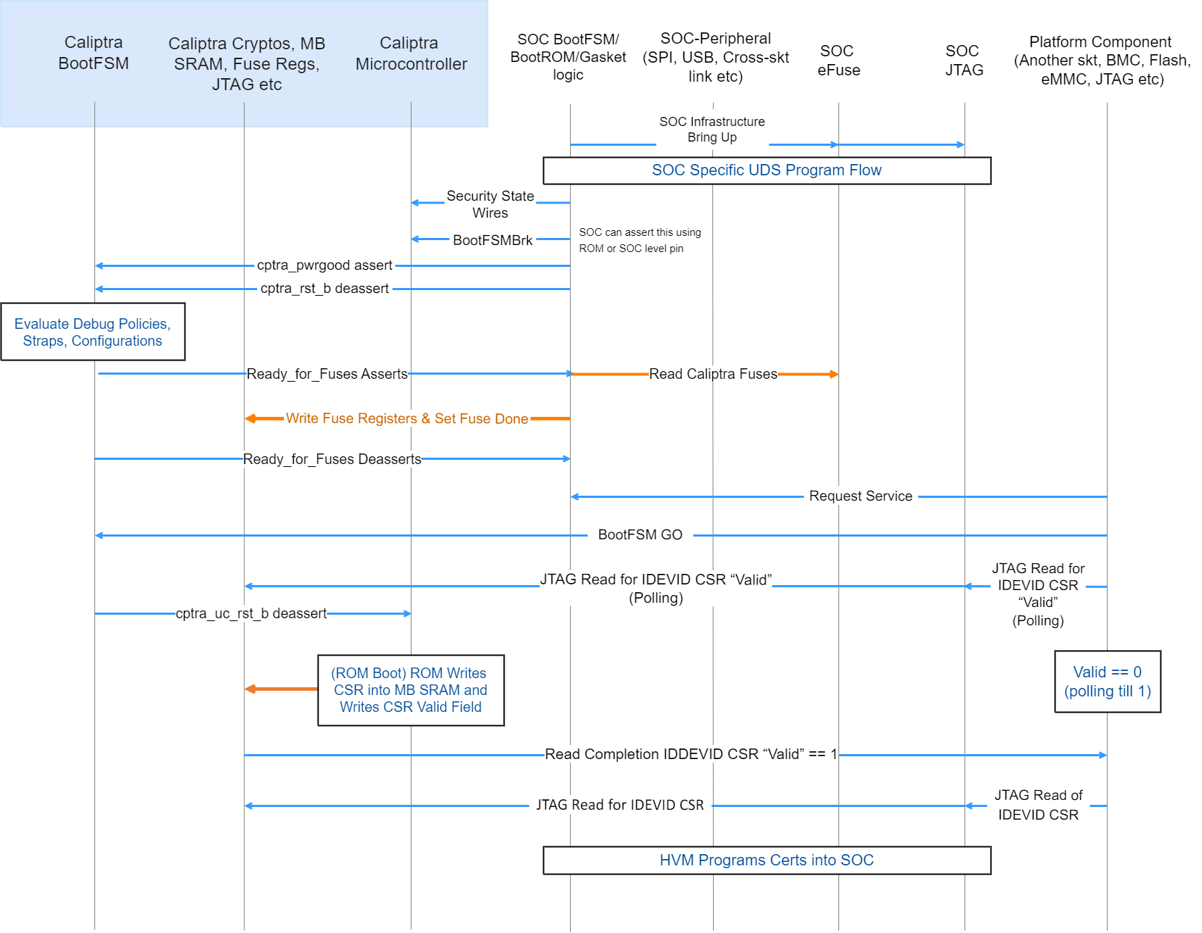
Figure 7: Passive Mode: Device manufacturing identity flow
- High Volume Manufacturing (HVM) programs the IDevID certificate attributes fuses. See IDevID Certificate for encodings.
- HVM programs NIST compliant UDS into fuses using SoC-specific fuse programming flow. Note that this UDS goes through an obfuscation function within Caliptra IP.
- SoC drives the security state, which indicates that it's a manufacturing flow. See Caliptra Security States for encodings.
- SoC (using a GPIO pin or SoC ROM) drives BootFSMBrk (this is also used for debug cases). This can be driven at any time before cptra_rst_b is deasserted.
- SoC follows the boot flow as defined in Caliptra IP HW boot flow to assert cptra_pwrgood and deassert cptra_rst_b, followed by writing to the fuse registers.
- HVM, through JTAG or using the Caliptra SoC interface, sets “CPTRA_DBG_MANUF_SERVICE_REG” bit 0 to request a CSR.
- HVM, through JTAG or using the Caliptra SoC interface, writes to “CPTRA_BOOTFSM_GO” to allow Caliptra’s internal BootFSM to continue to bring up microcontroller out of reset.
- ROM reads the manufacturing state encoding from the “CPTRA_DBG_MANUF_SERVICE_REG” register, acquires the mailbox lock, and populates the Caliptra internal SRAM (the mailbox SRAM hardware structure is reused) with the CSR.
- HVM, through JTAG or using the SoC interface, polls for the “IDevID CSR ready" bit 24 that is set in “CPTRA_FLOW_STATUS” register.
- HVM reads mbox_status[3:0] to check if the data is ready to be read (DATA_READY encoding).
- HVM must clear bit 0 of CPTRA_DBG_MANUF_SERVICE_REG, indicating that it completed reading the CSR.
- Caliptra ROM opens the Caliptra Mailbox for SoC usages, such as FW loading (if required in some HVM flows). The SoC is only allowed to request a lock of the AXI-exposed mailbox interface after this CSR operation is complete.
Certificate format
Caliptra certificates follow the X.509 v3 format described in RFC 5280. After vendor provisioning, Caliptra's certificate chain contains the following certificates:
- Provisioner CA (may be one or more certificates)
- IDevID
- LDevID
- AliasFMC
- AliasRT
- DPE
After owner provisioning, an Owner CA may endorse the IDevID, LDevID, or AliasFMC public keys. Owner CA provisioning is outside the scope of this specification.
Caliptra generates the LDevID, AliasFMC, AliasRT, and DPE certificates. The vendor, and optionally the owner, generate all other certificates.
Serial number algorithm
Caliptra uses certificate templates to avoid implementing fully capable X.509 v3 parsers and generators. Templates require certificates to be fixed length. This imposes constraints on the certificate serial numbers:
- Positive integer
- First octet as non-zero
- 20 octets in length
All Caliptra certificate serial numbers are generated with the following algorithm. The input is the certificate ECDSA or PQC MLDSA-87 public key in uncompressed form:
- Convert to DER format.
- Compute SHA256 digest.
- AND the least-significant-byte with ~0x80.
- OR the least-significant-byte with 0x04.
- Perform byte-wise copies of the least-significant 20 bytes into the certificate template.
Provisioner CA
Provisioner CA (pCA) is a set of one or more certificates issued by the vendor. The vendor is responsible for provisioning pCA to the SoC. Caliptra does not consume pCA. See Reference 5 for guidance on pCA.
IDevID certificate
The vendor issues the IDevID certificate during SoC manufacturing. As part of provisioning IDevID during manufacturing, Caliptra uses the UDS to derive the IDevID key pair and generate a CSR. The vendor's pCA uses the CSR to generate and sign the IDevID certificate. The CSR uses the format defined in PKCS#10.
For IDevID to endorse LDevID, Caliptra requires the vendor to implement an X.509 v3 IDevID certificate described in RFC 5280 with the field values specified in Table 7: IDevID certificate fields. The vendor shall also populate all extensions from the "Requested Extensions" attribute in the CSR. It is also recommended that the vendor add the Authority Information Access (AIA) extension to the IDevID certificate and maintain an Online Certificate Status Protocol (OCSP) responder with a URL pointed to by the AIA extension.
Table 7: IDevID certificate fields
| Field | Sub field | Value |
|---|---|---|
| Version | v3 | 2 |
| Serial Number | - | Generate with serial number algorithm using IDevID public key in uncompressed form |
| Validity | notAfter | 99991231235959Z |
| Subject Name | CN | Caliptra 1.0 IDevID |
| serialNumber | Hex-encoded printable string of SHA256 hash of DER-formatted IDevID public key in uncompressed form | |
| Subject Public Key Info | Algorithm | ecdsa-with-SHA384 |
| Parameters | Named Curve = prime384v1 | |
| Public Key | IDevID Public Key value | |
| Signature Algorithm Identifier | Algorithm | ecdsa-with-SHA384 |
| Parameters | Named Curve = prime384v1 | |
| Signature Value | - | Digital signature for the certificate |
| KeyUsage | keyCertSign | 1 |
| Basic Constraints | CA | TRUE |
| pathLen | 5 | |
| Subject Key Identifier | - | specified by IDevID attribute fuses |
| tcg-dice-Ueid | ueid | UEID specified by IDevID attribute fuses |
Caliptra does not consume the IDevID certificate. Caliptra needs attributes of the IDevID certificate in order to generate the Authority Key Identifier extension for the LDevID and to populate the TCG Universal Entity ID (UEID) extension for Caliptra-generated certificates. The vendor must fuse these attributes into the IDevID attribute fuses for Caliptra to consume. The encoding of these attribute fuses is as follows:
- Flags (byte 0, bits [1:0]): Key ID algorithm for IDevID Subject Key Identifier.
- 0 = SHA1 of DER-formatted IDevID public key in uncompressed form
- 1 = First 20 bytes of SHA256 of DER-formatted IDevID public key in uncompressed form
- 2 = First 20 bytes of SHA384 of DER-formatted IDevID public key in uncompressed form
- 3 = raw
- Reserved (bytes 1 to 3)
- Subject Key ID (bytes 4 to 23): if Flags = 3, the IDevID Subject Key Identifier to use as the LDevID Authority Key Identifier.
- UEID type (byte 24): UEID type as defined in the IETF EAT specification. Used for TCG UEID extension.
- Reserved (bytes 25 to 27)
- Manufacturer Serial Number (bytes 28 to 43): the 128-bit unique serial number of the device to be used for the TCG UEID extension in the Caliptra-generated LDevID, AliasFMC, and AliasRT certificates.
The IDevID certificate is unique for each device and non-renewable. The SoC must be able to retrieve the IDevID certificate at runtime. To save flash space and aid in recoverability, it is recommended that the vendor define an IDevID certificate template such that the SoC at runtime can reconstruct the same certificate that the pCA endorsed. The SoC is recommended to store the IDevID certificate signature in fuses and the IDevID certificate template in the firmware image. Caliptra runtime firmware provides APIs to aid in reconstructing the certificate:
- GET_IDEV_INFO to return the IDevID public key.
- GET_IDEV_CERT to return the certificate given a to-be-signed (TBS) payload and the certificate signature from fuses. The TBS is the certificate template already patched with the IDevID public key, Subject Key Identifier, serial number, and any extensions that are unique to the device that the vendor may have included.
Caliptra does not allocate fuses in its fuse map for the IDevID certificate signature. Caliptra allocates "IDEVID MANUF HSM IDENTIFIER" fuses that the vendor can use to aid certificate reconstruction.
LDevID certificate
Caliptra ROM generates the LDevID certificate and endorses it with the IDevID private key. The LDevID certificate implements the following field values:
Table 8: LDevID certificate fields
| Field | Sub field | Value |
|---|---|---|
| Version | v3 | 2 |
| Serial Number | - | Generate with serial number algorithm using LDevID public key in uncompressed form |
| Issuer Name | CN | Caliptra 1.0 IDevID |
| serialNumber | Hex-encoded printable string of SHA256 hash of DER-formatted IDevID public key in uncompressed form | |
| Validity | notBefore | 20230101000000Z |
| notAfter | 99991231235959Z | |
| Subject Name | CN | Caliptra 1.0 LDevID |
| serialNumber | Hex-encoded printable string of SHA256 hash of DER-formatted LDevID public key in uncompressed form | |
| Subject Public Key Info | Algorithm | ecdsa-with-SHA384 |
| Parameters | Named Curve = prime384v1 | |
| Public Key | LDevID Public Key value | |
| Signature Algorithm Identifier | Algorithm | ecdsa-with-SHA384 |
| Parameters | Named Curve = prime384v1 | |
| Signature Value | - | Digital signature for the certificate |
| KeyUsage | keyCertSign | 1 |
| Basic Constraints | CA | True |
| pathLen | 4 | |
| Subject Key Identifier | - | First 20 bytes of SHA256 hash of DER-formatted LDevID public key in uncompressed form |
| Authority Key Identifier | - | specified by IDevID attribute fuses |
| tcg-dice-Ueid | ueid | UEID specified by IDevID attribute fuses |
Caliptra does not generate an LDevID CSR. Owners that wish to endorse LDevID must do so with proprietary flows.
AliasFMC certificate
Caliptra ROM generates the AliasFMC certificate and endorses it with the LDevID private key. The AliasFMC certificate implements the following field values:
Table 9: AliasFMC certificate fields
| Field | Sub field | Value |
|---|---|---|
| Version | v3 | 2 |
| Serial Number | - | Generate with serial number algorithm using FMC Alias public key in uncompressed form |
| Issuer Name | CN | Caliptra 1.0 LDevID |
| serialNumber | Hex-encoded printable string of SHA256 hash of DER-formatted LDevID public key in uncompressed form | |
| Validity | notBefore | notBefore from firmware manifest |
| notAfter | notAfter from firmware manifest | |
| Subject Name | CN | Caliptra 1.0 FMC Alias |
| serialNumber | Hex-encoded printable string of SHA256 hash of DER-formatted FMC Alias public key in uncompressed form | |
| Subject Public Key Info | Algorithm | ecdsa-with-SHA384 |
| Parameters | Named Curve = prime384v1 | |
| Public Key | FMC Alias Public Key value | |
| Signature Algorithm Identifier | Algorithm | ecdsa-with-SHA384 |
| Parameters | Named Curve = prime384v1 | |
| Signature Value | - | Digital signature for the certificate |
| KeyUsage | keyCertSign | 1 |
| Basic Constraints | CA | True |
| pathLen | 3 | |
| Subject Key Identifier | - | First 20 bytes of SHA256 hash of DER-formatted FMC Alias public key in uncompressed form |
| Authority Key Identifier | - | First 20 bytes of SHA256 hash of DER-formatted LDevID public key in uncompressed form |
| tcg-dice-Ueid | ueid | UEID specified by IDevID attribute fuses |
| tcg-dice-MultiTcbInfo | Flags | NOT_CONFIGURED if lifecycle is unprovisioned |
| NOT_SECURE if lifecycle is manufacturing | ||
| DEBUG if not debug locked | ||
| SVN | [2] Image Bundle FW SVN | |
| FWIDs | [0] SHA384 digest of | |
| Owner Public Key Hash (sha-384) | ||
| Owner public key Hash in fuses flag (u8) // Flag to indicate whether Owner Pub Key Hash is Fused | ||
| Anti-rollback disable Fuse (u8) | ||
| ECC Revoke Fuse (u8) | ||
| LMS Revoke Fuse (u32) | ||
| ML-DSA Revoke Fuse (u8) | ||
| Image Bundle FW min SVN Fuse - min SVN value (u8) | ||
| Auth Manifest SoC min SVN Fuse - min SVN value (u8) | ||
| Auth Manifest SoC max SVN Fuse - max SVN value (u8) | ||
| [1] SHA384 digest of | ||
| Vendor Public Key Hash Fuse (sha-384) | ||
| LMS Verify/PQC Type Fuse (u8) | ||
| Lifecycle State Wire (u8) | ||
| Debug Lock Wire (u8) | ||
| Image Bundle FW SVN from cold boot (u8) | ||
| PK Index ECC (u8) | ||
| PK Index PQC (u8) | ||
| [2] SHA384 digest of FMC | ||
| Type | [0] CALIPTRA_2_X_FUSE_OWNER_INFO | |
| [1] CALIPTRA_2_X_FUSE_VENDOR_INFO | ||
| [2] CALIPTRA_2_X_FMC_FIRMWARE_INFO |
MultiTcbInfo Extension
The MultiTcbInfo extension contains three TCBInfo entries, each corresponding to a unique target environment, attested by Caliptra ROM:
-
TCBInfo[0] - Platform Owner Fuse Configuration
- Type: CALIPTRA_2_X_FUSE_OWNER_INFO
- Corresponds to the fuse configuration owned by the platform owner
- Scope: Owner-controlled security settings (key hashes, revocation, anti-rollback)
-
TCBInfo[1] - Platform Vendor Fuse Configuration
- Type: CALIPTRA_2_X_FUSE_VENDOR_INFO
- Corresponds to the fuse configuration owned by the platform vendor (Caliptra integrator)
- Scope: Vendor-controlled security settings (vendor key, lifecycle, debug state)
-
TCBInfo[2] - FMC Firmware Measurement
- Type: CALIPTRA_2_X_FMC_FIRMWARE_INFO
- Corresponds to the digest of the FMC
- Scope: First Mutable Code firmware digest
- SVN: Firmware security version number
AliasRT certificate
Caliptra FMC generates the AliasRT certificate and endorses it with the AliasFMC private key. The AliasRT certificate implements the following field values:
Table 10: AliasRT certificate fields
| Field | Sub field | Value |
|---|---|---|
| Version | v3 | 2 |
| Serial Number | - | Generate with serial number algorithm using RT Alias public key in uncompressed form |
| Issuer Name | CN | Caliptra 1.0 FMC Alias |
| serialNumber | Hex-encoded printable string of SHA256 hash of DER-formatted FMC Alias public key in uncompressed form | |
| Validity | notBefore | notBefore from firmware manifest |
| notAfter | notAfter from firmware manifest | |
| Subject Name | CN | Caliptra 1.0 Rt Alias |
| serialNumber | Hex-encoded printable string of SHA256 hash of DER-formatted RT Alias public key in uncompressed form | |
| Subject Public Key Info | Algorithm | ecdsa-with-SHA384 |
| Parameters | Named Curve = prime384v1 | |
| Public Key | RT Alias Public Key value | |
| Signature Algorithm Identifier | Algorithm | ecdsa-with-SHA384 |
| Parameters | Named Curve = prime384v1 | |
| Signature Value | - | Digital signature for the certificate |
| KeyUsage | keyCertSign | 1 |
| Basic Constraints | CA | True |
| pathLen | 2 | |
| Subject Key Identifier | - | First 20 bytes of SHA256 hash of DER-formatted RT Alias public key in uncompressed form |
| Authority Key Identifier | - | First 20 bytes of SHA256 hash of DER-formatted FMC Alias public key in uncompressed form |
| tcg-dice-Ueid | ueid | UEID specified by IDevID attribute fuses |
| tcg-dice-TcbInfo | SVN | Firmware SVN |
| FWIDs | SHA384 digest of RT | |
| Type | CALIPTRA_2_X_RT_FIRMWARE_INFO |
TcbInfo Extension
The TcbInfo extension corresponds to the Caliptra Runtime Firmware target environment, attested by Caliptra FMC:
- TCBInfo - RT Firmware Measurement
- Type: CALIPTRA_2_X_RT_FIRMWARE_INFO
- Corresponds to the digest of the Caliptra Runtime Firmware
- Scope: Caliptra Runtime Firmware
- SVN: Firmware security version number
DPE certificate
Caliptra RT generates the DPE certificate and endorses it with the AliasRT private key. The DPE certificate fields are described in the Caliptra Runtime specification. DPE also supports issuance of CSRs.
Caliptra security states
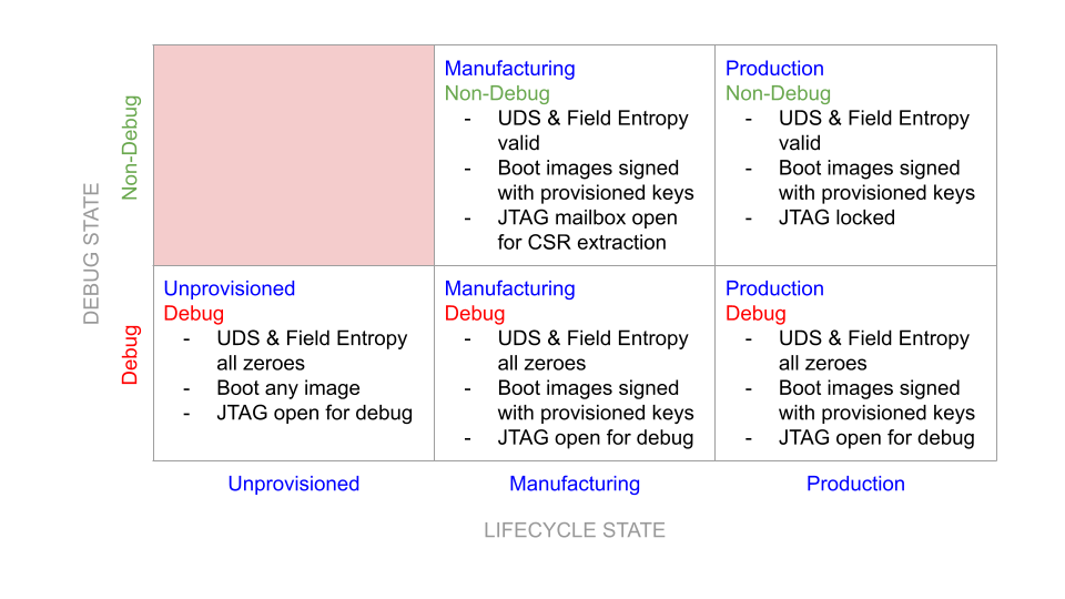
Figure 6: Caliptra security states
Definitions
- Non-Debug: Caliptra JTAG is not open for microcontroller and HW debug. Alias: DebugLocked
- Debug: Caliptra JTAG is open for microcontroller and HW debug. Alias: DebugUnlocked
- Unprovisioned: Blank/unprogrammed fuse part.
- Manufacturing: Device is in the manufacturing flow where HVM Caliptra fuses are programmed.
- Production: All of Caliptra’s HVM fuses are programmed.
- Secure: Any security state that restricts access to Caliptra from an external entity and has a known, specified function in the device lifecycle. Requires DebugLocked and either the Manufacturing or Production configuration.
- Insecure: Any security state other than those deemed secure. This includes all undefined states, all states with DebugUnlocked, and the Unprovisioned state. In accordance with the threat model, these states are considered a potential risk due to attacks via DFT or DFD channels, exploitation of unforeseen logic issues, or undefined behavior. These insecure states necessitate flushing of Caliptra secrets.
Notes:
- Caliptra’s security state is determined by the SoC’s security state and the SoC device lifecycle state.
- Caliptra’s state is considered a mode of operation.
- Caliptra security state is defined by the uppermost bit of the encoding below; 1=DebugLocked and 0=DebugUnlocked.
- Lower 2 bits are mapped to device lifecycle (unprovisioned, manufacturing, production).
- SoC’s security state may also be influenced by its own device lifecycle. A HW state machine must drive the SoC security state.
- Caliptra’s security state determines Caliptra’s debug state and the state of its security assets.
- In general, if Caliptra is in an insecure state, all keys and assets are ‘zeroized’. Zeroized may mean switching to all 0s, 1s, or debug keys based on the key. See Caliptra Assets for information.
Table 11: Security states
| Security state, device lifecycle state [2:0] | State | Definition | State transition requirement |
|---|---|---|---|
| 000b | DebugUnlocked and unprovisioned | This shall be the default state value for Caliptra’s security state; it is used for development and early Caliptra bring up. This state is not used to provision the Caliptra assets. In this state: - UDS and all other identity critical assets shall not be programmed in fuses. Un-programmed fuse bits shall be read as 0s (zero). The debug UDS shall be obfuscated and de-obfuscated using the debug obfuscation key. - Obfuscation key: The debug obfuscation key shall be used. - Caliptra JTAG is unlocked and allows microcontroller debug. - Caliptra JTAG can access IP internal registers through FW. | Unprovisioned to any other state requires a cold boot of Caliptra and SoC. |
| 101b | DebugLocked and manufacturing | Caliptra must be placed in this state during the secure HVM process. In this state: - UDS and other identity critical assets shall be programmed into fuses. They are written into Caliptra fuse registers, similar to the ‘Secure’ state. - All security assets shall be in production mode (production UDS and obfuscation shall be used). - Upon pwrgood assertion, Caliptra JTAG shall be locked; microcontroller debug shall be disabled. - Caliptra microcontroller can be interrupted through JTAG mailbox. | Manufacturing -> insecure state transition is allowed with warm reset and Caliptra clears all of the security critical assets and registers before JTAG is opened. Manufacturing -> secured state is allowed ONLY with a cold boot. See Provisioning During Manufacturing for details. |
| 111b | DebugLocked and production | All security assets are in production mode. In this state: - Production UDS and obfuscation key shall be used. - CPU execution shall be enabled. - All ‘backdoor’ functionality shall be disabled (for example, developer functions and functionality that could reveal sensitive information or result in escalation of privileges). - Debug functions shall be disabled. Caliptra JTAG is locked – microcontroller debug shall be disabled. Caliptra microcontroller shall not be interruptible through JTAG mailbox. - DFT functions shall be disabled. | DebugLocked -> DebugUnlocked is possible without cold boot and Caliptra clears all of the security critical assets and registers before JTAG is opened. |
| 011b | DebugUnlocked and production | This state is used when debugging of Caliptra is required. When in this state: UDS and other identity critical assets are programmed into fuses. They may not have been written into Caliptra fuse registers if the insecure state entered before Caliptra is out of reset. If the insecure state transition happened after fuses are written to Caliptra, they are cleared when the security state transitions from secure/production -> insecure. Caliptra state: All security assets are in debug mode (UDS and obfuscation key are in production state). - UDS: Reverts to a ‘well-known’ debug value. - Obfuscation key: Switched to debug key. - Key Vault is also cleared. - Caliptra JTAG is unlocked and allows microcontroller debug. - Caliptra JTAG can access IP internal registers through FW or directly. | DebugUnlocked -> DebugLocked is allowed ONLY with a cold boot. |
Notes:
- End-of-life state is owned by SoC. In end-of-life device lifecycle state, Caliptra shall not not be brought out of reset.
- Other encodings are reserved and always assumed to be in a secure state.
Each of these security states may be mapped to different SoC level debug and security states. SoC’s requirement is that if the SoC enters a debug state, then Caliptra must also be in an insecure state where all assets are cleared. Caliptra security state is captured by hardware on every warm reset; therefore SoC integrators enforce the security state transition policies for cold boot events. These policies are described in the preceding table.
Service surface
The service surface of Caliptra has multiple vectors. All use cases are control plane services, useful to power on a system or start a task. Supporting line rate high performance IO cryptography or any other data path capability is not required.
- Logic IOs: Required to indicate status of the IP, availability of a message through AXI, and to enable or disable certain debug capabilities (like JTAG enable or disable).
- Command mailbox: Caliptra shall offer services to other parts of the SoC. The APIs are documented in the Caliptra Runtime specification and summarized below:
- Loading firmware: Caliptra firmware is loaded via the mailbox at cold boot. In addition, Caliptra firmware can be loaded at runtime to support hitless or impactless updates.
- DICE-as-a-Service: Caliptra shall expose the TCG DICE Protection Environment iRoT Profile API, allowing Caliptra to derive and wield a DICE identity on behalf of other elements within the SoC. For example, Caliptra can sign messages for an SPDM responder.
- Measurement Vault: Caliptra shall support stashing of measurements for the code and configuration of the SoC. Caliptra can provide these measurements via PCR Quote API or via DPE.
- FW Authentication: Caliptra supports ECDSA and PQC MLDSA-87 verification for SoC firmware beyond its own. The SHA384 block exposes a HW API for hashing firmware. The runtime firmware exposes an ECDSA and MLDSA-87 verification API that uses the hash computed by the SHA384 block.
Device resilience
As noted earlier, Caliptra plays a role in maintaining the resilience posture of the SoC as defined by NIST SP 800-193 Platform Firmware Resiliency Guidelines (see Reference 1). As the Silicon RTM and RTI, Caliptra is either responsible for, or participates in, various protection and detection requirements described in the NIST publication.
The following table describes the NIST SP 800-193 requirements that Caliptra shall meet, either on its own or in conjunction with other components within the SoC or platform. Requirements not listed are assumed to be not covered and out-of-scope for Caliptra. In particular, most requirements related to firmware update and recovery are out-of-scope and must be handled by other components of the system.
Table 12: NIST SP 800-193 requirements
| NIST SP 800-193 Chapter | Requirement | Caliptra responsibility |
|---|---|---|
| 4.1.1 | All security mechanisms and functions shall be founded to Roots of Trust (RoT). | Caliptra forms the basis for all trust in the SoC starting from execution of its immutable ROM. See the Secure Boot Flow section. |
| 4.1.1 | If Chains of Trust (CoT) are used, RoT shall serve as the anchor for the CoT. | Caliptra firmware shall be authenticated and executed as part of a Chain of Trust extended from the Caliptra ROM, while all other firmware shall be measured into a CoT extended from the Caliptra ROM. See the Secure Boot Flow section. |
| 4.1.1 | All RoTs and CoTs shall either be immutable or protected using mechanisms that ensure all RoTs and CoTs remain in a state of integrity. | Caliptra firmware is authenticated and executed as part of a Chain of Trust extended from the Caliptra ROM. See the Secure Boot Flow section. The SoC or platform is responsible for maintaining integrity for other elements of the CoT. |
| 4.1.1 | All elements of the CoT for update, detection, and recovery in non-volatile storage shall be implemented in platform firmware. | Caliptra forms the basis for RTM, which the SoC can use to create detection capabilities. All other silicon RoT capabilities are extended by additional firmware loaded in the SoC and anchored by Caliptra. |
| 4.1.1 | The functions of the RoTs or CoTs shall be resistant to any tampering attempted by software running under, or as part of, the operating system on the host processor. | Caliptra shall run on a dedicated microcontroller, isolated physically from access by other components in the system. |
| 4.1.1 | Information transferred from the software on the host processor to the platform firmware shall be treated as untrusted. | Caliptra shall verify the authenticity of its firmware using an approved digital signature verification mechanism. |
| 4.1.1 | CoTs may be extended to include elements that are not from non-volatile storage. Before use, those elements shall be cryptographically verified by an earlier element of the CoT. | Caliptra shall verify the authenticity of its firmware using an approved digital signature verification mechanism. Caliptra shall also collect the measurement of the SoC security processor FMC code before it is verified and executed by the SoC. |
| 4.1.2 | If the key store is updateable, then the key store shall be updated using an authenticated update mechanism, absent unambiguous physical presence through a secure local update. | Hashes for the keys used to authenticate Caliptra FW are programmed into fuses during manufacturing. If a key is deemed to be compromised, that key may be revoked and the next key used instead. |
| 4.1.3 | Each platform device that implements a detection capability shall rely on either a Root of Trust for Detection (RTD), or a Chain of Trust for Detection (CTD). The CTD is anchored by an RTD for its detection. | Caliptra forms the basis for RTM, which the SoC can use to create detection capabilities. Caliptra firmware shall be authenticated and executed as part of a Chain of Trust extended from the Caliptra ROM, while all other firmware shall be measured into a CoT extended from the Caliptra ROM. See the Secure Boot Flow section. |
| 4.1.3 | The RTD or CTD shall include or have access to information necessary to detect corruption of firmware code and critical data. | Caliptra relies on hashes of authorized keys stored in fuses. Those hashes are then checked against public keys found in firmware headers to authenticate Caliptra’s runtime firmware. Caliptra relies on redundancy in the fuses to protect the key and configuration data. |
| 4.2.3 | If critical platform firmware code in non-volatile memory is copied into RAM to be executed (for performance, or for other reasons) then the firmware program in RAM shall be protected from modification by software or shall complete its function before software starts. | Caliptra shall run on a dedicated microcontroller, isolated physically from access by other components in the system. |
| 4.2.3 | If critical platform firmware uses RAM for temporary data storage, then this memory shall be protected from software running on the platform until the data’s use is complete. | Caliptra shall run on a dedicated microcontroller, isolated physically from access by other components in the system. |
| 4.2.3 | Software shall not be able to interfere with the intended function of critical platform firmware. For example, by denying execution, modifying the processor mode, or polluting caches. | Caliptra shall run on a dedicated microcontroller, isolated physically from access by other components in the system. In addition, the Caliptra subsystem begins execution before other firmware is allowed to run. |
| 4.2.4 | Critical data shall be modifiable only through the device itself or defined interfaces provided by device firmware. Examples of defined interfaces include proprietary or public application programming interfaces (APIs) used by the device’s firmware, or standards-based interfaces. Symbiont devices may rely on their host devices to meet this requirement. | Caliptra receives firmware and configuration input only via defined interfaces within the SoC. See the Mailbox section. |
| 4.2.1.3 | The authenticated update mechanism shall be capable of preventing unauthorized updates of the device firmware to an earlier authentic version that has a security weakness or would enable updates to a version with a known security weakness. | Caliptra supports a mechanism for detecting and preventing execution of a prior firmware image that is no longer authorized. See the Anti-rollback Support section. |
| 4.3.1 | A successful attack that corrupts the active critical data or the firmware image, or subverts their protection mechanisms, shall not in and of itself result in a successful attack on the RTD or the information necessary to detect corruption of the firmware image. | Caliptra shall verify the signature of any firmware it loads during each boot. If the signature verification fails, Caliptra shall notify the SoC that firmware recovery must be performed. See the Error Reporting and Handling section. |
| 4.3.1 | Verify integrity, using an approved digital signature algorithm or cryptographic hash, of device firmware code prior to execution of code outside the RTD. | Caliptra shall perform digital signature verification of its firmware before it is allowed to execute. |
| 4.3.1 | If firmware corruption is detected, the RTD or CTD should be capable of starting a recovery process to restore the device firmware code back to an authentic version. | Caliptra shall notify the SoC via the Mailbox interface to initiate the recovery process. |
| 4.3.1 | The detection mechanism should be capable of creating notifications of firmware corruption. | Caliptra shall notify the SoC via the Mailbox interface to initiate the recovery process. |
| 4.3.1 | The detection mechanism should be capable of logging events when firmware corruption is detected. | It is the responsibility of the SoC to log any corruption events upon notification by Caliptra. |
| 4.3.2 | The RTD or CTD shall perform integrity checks on the critical data prior to use. Integrity checks may take the form, for example, of validating the data against known valid values or verifying the hash of the data storage. | Caliptra relies on SoC fuse integrity to store its configuration data, which is owned and passed to Caliptra through the Mailbox. |
| 4.3.2 | The RTD or CTD should be capable of creating notifications of data corruption. | See the Error Reporting and Handling section. |
| 4.3.2 | The detection mechanism should be capable of logging events when data corruption is detected. | It is the responsibility of the SoC to log any corruption events upon notification by Caliptra. |
Secure boot flow
Caliptra shall follow and implement the secure boot guidelines as described in Reference 3.
For the detailed flow, see the hardware section and firmware verifcation section.
Hitless update
A ‘hitless’ (aka ‘impactless’) update occurs when an update is applied to Caliptra’s executing firmware without requiring a SoC or machine reboot. A hitless update allows Caliptra FW4 to remain up to date with FW security and/or functional patches while preventing or reducing machine downtime. Hitless update shall take effect immediately upon application (post-cryptographic verification). Updates to the machine’s persistent storage are still required because they ensure that Caliptra reboots to the latest FW if the system requires a restart or reboot.
Caliptra contains multiple hardware isolated registers for Platform Configuration Registers (PCR). These PCRs serve as volatile storage for concise cryptographic measurement of security state, including Caliptra’s own firmware.
Journey measurements matter because hitless updates are a challenge for devices that only capture their current firmware version and state. This is particularly true when the previous state may have impacted the current state of dependent components within the SoC. For example, a device might move from firmware version A to firmware version B without assuming a clean start to flush state. Vulnerabilities in firmware version A might impact version B. Preserving a device boot measurement and currently running measurement can highlight differences, but preserving these measurements does not distinguish between transitional states, such as when intermediate updates have the potential to expose the device to vulnerabilities. For example, a device may move from firmware version A, to B, and then to C without a restart, whereas another device of the same type might transition from A to C without transitioning through B. If tracking only the boot and current firmware version, should a vulnerability be found in version B, it is impossible to identify which devices transitioned through B compared to devices that transitioned from A to C directly.
To capture all firmware and configuration changes, Caliptra tracks and attests to both current measurements and cumulative measurement PCR banks. The current measurement is a snapshot of the currently running firmware and configuration. This provides easy reference for the current version. If the current and cumulative measurements are different, it can safely be assumed that the device has undergone some update. The cumulative measurement captures all of the firmware and state transitions from a clean cold boot to the current version. The cumulative measurement must be accompanied by a log structure that describes the path from boot to current measurement using hash extensions. A verifier can understand a device’s path to its current state by replaying log entries to reconstruct the cumulative measurement.
The log and cumulative measurement mechanism is similar to that used in TPM. In this model, Caliptra only needs to securely manage the measurements; the log does not need to be secured or maintained by Caliptra or the SoC. The construction of measurements through cryptographic hash extensions means that the log must provide the exact order and evidence needed to reconstruct the measurement. As such, the log is tamper evident by design and does not need to be kept secure.
Caliptra contains 32 384-bit PCR banks that are extendable by the SHA engine, and readable by Caliptra firmware. The usage of the PCR banks is as follows:
Table 13: PCR bank usage
| PCR number | Type | Extend control | Description |
|---|---|---|---|
| PCR0 | Current | ROM | Holds Caliptra’s FMC measurement and ROM policy configuration. |
| PCR1 | Cumulative | ROM | Holds journey of Caliptra’s FMC measurement and ROM policy configuration. |
| PCR2 | Current | FMC | Holds Caliptra's runtime firmware and firmware manifest measurements. |
| PCR3 | Cumulative | FMC | Holds journey of Caliptra's runtime firmware and firmware manifest measurements. |
| PCR4 to PCR30 | - | RT | Holds measurements extended by EXTEND_PCR commands (serviced by RT). |
| PCR31 | Cumulative | ROM | Holds measurements extended by STASH_MEASUREMENTS commands (serviced by both ROM and RT). |
For PCR0 and PCR1, ROM issues the following extend operations in order:
- An array containing the following fields as 8-bit values:
- Lifecycle state
- Debug locked state
- Anti-rollback disable fuse
- ECDSA vendor public key index
- MLDSA-87 vendor public key index
- Cold-boot firmware SVN
- Effective Fuse SVN (i.e., 0 if anti-rollback disable is set)
- LMS vendor public key index
- LMS verification enable fuse
- Boolean indicating whether the owner public key hash is in fuses
- Vendor public key hash
- Owner public key hash
- Digest of FMC
Caliptra ROM fails to boot if the following values do not remain constant across a hitless update:
- Owner public key hash
- ECDSA vendor public key index
- MLDSA-87 vendor public key index
- LMS vendor public key index
- FMC digest
Attestation of Caliptra's update journey
Upon every cold boot and hitless update, Caliptra ROM extends Caliptra's FMC measurement and ROM policy configuration into PCR0 (current) and PCR1 (cumulative). Upon every cold boot and hitless update, Caliptra FMC extends Caliptra's runtime firmware and firmware manifest measurements into PCR2 (current) and PCR3 (cumulative). The current measurement of the FMC, ROM policy configuration, RT, and FW manifest are used to derive a CDI and an alias key given to runtime firmware. FMC places runtime firmware's measurements into runtime firmware's alias key certificate, and signs that certificate with FMC's alias key.
When runtime firmware boots following a hitless update, it will use the following pieces of data for building the DPE nodes and certificate chain:
- Its CDI, derived by FMC
- Its alias key, generated by FMC
- Its alias certificate, signed by FMC
- Its journey measurements in PCR3, extended by FMC
- SRAM state, established by the prior runtime firmware image
SRAM state consists of measurements captured by prior runtime firmware images, and does not contain secrets or executable data5. Therefore, the trustworthiness of runtime firmware is reflected in the measurements captured by FMC and is evident in the runtime firmware alias certificate.
Caliptra firmware will attest to PCR3 by including it as an input in all DPE leaf key derivations and as evidence in all DPE leaf key certificates.
Commentary: recovery from a bad hitless update
Suppose the following Caliptra firmware images exist:
- Version A: presumed-good
- Version B: known-bad
- Version C: presumed-good
A remote verifier wishes to confirm that a given Caliptra device has not run version B since cold boot. The remote verifier can challenge the SoC with a freshness nonce; higher-layer software passes that freshness nonce as a request to Caliptra's DPE for signing. The remote verifier receives the following pieces of evidence:
- An endorsement over LDevID, which may take a number of forms, including:
- Caliptra's vendor-signed certificate over IDevID, and an IDevID-signed certificate over LDevID.
- An owner-signed certificate over IDevID, and an IDevID-signed certificate over LDevID.
- An owner-signed certificate over LDevID.
- An LDevID-signed certificate over AliasFMC, which includes FMC's measurements as captured by ROM.
- An AliasFMC-signed certificate over AliasRT, which includes runtime firmware's measurements as captured by FMC.
- An AliasRT-signed certificate over a leaf DPE key, which includes PCR3 as read by runtime firmware, along with other measurements previously stashed in SRAM.
- A log structure6 that represents the measurements that have been extended into PCR3.
- A leaf-DPE-signed blob7 containing the freshness nonce.
The remote verifier evaluates (1) according to ownership policies to determine whether the Caliptra device is trustworthy, before proceeding to verify the rest of the attestation response.
Thus satisfied in the trustworthiness of the Caliptra device, the remote verifier can then evaluate the trustworthiness of FMC by inspecting the measurements in (2), AliasFMC's certificate. The verifier can reject the attestation if those measurements do not conform to a known-good value.
Thus satisfied in the trustworthiness of FMC, the remote verifier can then evaluate the trustworthiness of runtime firmware by inspecting the measurements in (3), AliasRT's certificate. If version A or C is running, then the PCR3 measurement present in (4), the leaf DPE key certificate, is presumed to be an honest reflection of the hardware register as read by runtime firmware. The verifier can reject the attestation if AliasRT's certificate indicates that version B is currently running.
Thus satisfied that version B is not currently running and that PCR3 is an accurate reflection of the hardware register, the remote verifier can then compare the log in (5) to PCR3 in (4) to confirm its authenticity, then walk the log to confirm that FMC never launched version B since cold-boot. If version B did run, that firmware could have maliciously modified DPE measurements stashed in SRAM, but could not have modified the contents of PCR3 to erase the evidence that version B ran at all, and could not have influenced the behavior of firmware versions A or C to prevent them from accurately reporting the contents of PCR3.
Thus satisfied that version B has not run since power-on, the verifier can also optionally inspect other measurements in (4) to evaluate the journey of other SoC components, whose measurements were previously stored within Caliptra's SRAM.
Finally, the verifier can confirm freshness by comparing the nonce in (6) to the one emitted in the original challenge. Because DPE only allows a derived leaf key to be used if the measurements present in its leaf certificate are a reflection of the current state, the fact that the freshness nonce was signed by DPE is evidence that the measurements in (4) are fresh.
Commentary: maintaining sealed secrets across a power cycle
Caliptra does not seal secrets directly. However, Caliptra does implement DPE, which allows secrets to be sealed to an external sealer such as a TPM, with a policy that only allows those secrets to be unsealed if Caliptra allows the host to wield a particular leaf DPE key. This leaf DPE key is permuted based on the hitless update journey of the various components whose measurements are stored within Caliptra.
This poses a challenge for maintaining sealed secrets across a power cycle. Suppose the SoC cold booted CPU microcode A, then hitlessly updated to B, and then to C. The measurements stored within Caliptra's SRAM will represent the [A->B->C] update journey, and DPE's leaf key is derived based on this journey.
Let us assume that upon each hitless update, the firmware update is also written to persistent storage, such that on the next cold boot the new firmware will run. Thus, on the next boot, the SoC's microcode update journey is simply [C]. This is a different journey than [A->B->C], and so DPE's leaf key will differ. The old secret sealed to the old DPE leaf key is no longer accessible to the SoC.
To anticipate this eventuality, before a power cycle, the SoC can instruct DPE to predict what the DPE leaf public key will be if the microcode journey is simply [C], using DPE's simulation context. The SoC can then reseal secrets to the external sealer with a policy that can be satisfied if the computed public key is used.
Note: as all DPE leaf keys are derived using Caliptra runtime firmware's CDI, a DPE simulation context cannot predict the leaf key that would be available if a different Caliptra firmware image were to boot (because one Caliptra firmware image does not have access to a different image's CDI). Therefore, if a different Caliptra firmware image is staged to persistent storage, Caliptra must first be hitlessly updated to that image before a simulation context can be used to predict public keys that will be available to that image on the next cold boot.
Attestation of SoC update journey
Caliptra shall also attest to the journeys of SoC components. A SoC component's journey may change independently of other components. For example, SoC components may implement partial resets or hitless updates that cause the component's firmware or configuration to reload.
Caliptra shall maintain a reboot counter for each component. Caliptra shall increment the reboot counter and update the journey measurement for calls that indicate that the component's state changed. Caliptra shall attest the journey measurement and report the counter value on-demand. The verifier is assumed to have knowledge of update events at an associated reboot counter (via an event log) but not have knowledge of reset events. The verifier can compute the journey measurement via multiplicatively extending the current measurement by the reset counter. For example:
- Upon cold boot, SoC component boots firmware A. Reboot counter is 0. The tuple of (0,A) is in the event log.
- SoC component is partial reset once. Reboot counter is 1.
- SoC component is hitlessly updated to firmware B. Reboot counter is 2. The tuple of (2,B) is in the event log.
- SoC component is partial reset twice. Reboot counter is 4.
The corresponding journey measurement computation is the chained extension of [A->A->B->B->B]. The verifier can ascertain this through the two event log entries.
Anti-rollback support
Caliptra shall provide fuse banks (refer to Table 21: Caliptra Fuse Map) that are used for storing monotonic counters to provide anti-rollback enforcement for Caliptra mutable firmware. Each distinctly signed boot stage shall be associated with its own anti-rollback fuse field. Together with the vendor, Caliptra allows owners to enforce strong anti-rollback requirements, in addition to supporting rollback to a previous firmware version. This is a critical capability for hyperscalers.
Caliptra firmware shall include an SVN value in the signed header. If the firmware's SVN value is less than the current counter value in the fuse bank, Caliptra shall refuse to boot that firmware, regardless of whether the signature is valid.
Alternatively, platform vendors may prefer to manage firmware storage and rollback protection in a different manner, such as through a dedicated Platform RoT. In such cases, the vendor may wish to disable anti-rollback support from Caliptra entirely. This disable support is available via an OTP/fuse setting.
Each of Caliptra's internal anti-rollback fuse banks shall support a minimum counter value of 64. This feature is expected to be used sparingly.
Physical attack countermeasures
Caliptra shall implement countermeasures designed to deter both glitching (also referred to fault-injection (FI)) and side-channel attacks (simple power analysis (SPA) and differential power analysis (DPA)).
The Caliptra threat model guides the priority of which physical countermeasures are based on a specific physical implementation.
From the top, an adversary in the supply chain has essentially unlimited time to glitch the chip and make it reveal any private key material or symmetric secrets. One Glitch To Rule Them All is one example with recency bias. The most critical countermeasures must prevent non-destructive extraction of those secrets. Otherwise, an adversary who succeeds can silently impersonate production-serving assets at a later time.
Randomly generated per-part entropy is subject to physical inspection attacks in the supply chain as well. The fuses that store the UDS entropy shall be protected to a degree that forces an attacker to perform a destructive operation to read their values. Decapping and fibbing attacks should at least penetrate enough layers and metal shielding to render the part useless, if not being outright impossible to carry out. Entropy tied to a damaged asset typically requires injection of counterfeit devices in the supply chain, which is a very powerful adversary model.
Another way to obtain access to secret entropy with “unlimited supply chain time” is to observe side channels while the SoC is executing. Because Caliptra is expected to be a <1 mm2 fraction of a large SoC, side-channel mitigation is required only against extremely resourceful attackers that can wade through and discern a large number of confounding signals and power profiles. With that priority in mind, DPA and DMA attacks should be mitigated via decoy value generation.
Any private key material or symmetric key material embedded in the RTL (and therefore “global”) must be treated as having low value, reaching zero value in a number of quarters. A supply chain attacker can destructively obtain the key material, and loss of one part is not going to trigger any alarms.
Mitigation against SCA is not trivial and may be implemented in a variety of ways. Reference 7 provides a comprehensive overview of methods and techniques used in various SCA as well as recommendations for countermeasures against such attacks (including feasibility and applicability). Additionally, there are academic papers available from NIST and other resources that discuss SCA and their countermeasures.
Compliance and certification requirements
Due to the identity service surface offered to other SoC subsystems, Caliptra may fall under the Target of Evaluation (ToE) of an application that wishes to attain a specific compliance level for business reasons.
It is important to highlight that it’s not necessary for the RTM itself to unilaterally attain (for example, FIPS 140-3 L3). It is only relevant when the RTM is included in the “bag” that wants to obtain a compliance certification. For example, it is relevant when a cloud provider wants to FIPS-certify PCIe link encryption in transit rooted to an ASIC identity emanating from a Caliptra instance.
See Reference 8 for requirements related to keys, entropy, random bits, cryptographic modules, and algorithms.
Known Answer Test (KAT) support
To certify a cryptographic module, pre-operational self-tests must be performed when the system is booted. Implementing KATs is required for FIPS certification. However, regardless of FIPS certification, it is considered a security best practice to ensure that the supported cryptographic algorithms are functioning properly to guarantee correct security posture.
KAT execution is described as two types:
- Pre-operational Self-Test (POST)
- Conditional Algorithm Self-Test (CAST)
A detailed description of the POST and CAST KATs can be found at csrc.nist.gov.
Table 14: KAT failure mitigations
| KAT type | If fails |
|---|---|
| POST | Failure of a POST KAT (for example, ECDSA) shall result in Caliptra boot failure. A reset may or may not result in successful POST completion. |
| CAST | Failure of a CAST KAT shall cause Caliptra to fail any operation that has a dependency on the associated cryptographic algorithm. |
Table 15: POST/CAST usage
| Crypto algorithm | Caliptra Boot ROM | Caliptra FMC | Caliptra Runtime FW |
|---|---|---|---|
| ECDSA8 | Yes | Yes | Yes |
| MLDSA-878 | Yes | Yes | Yes |
| AES | Yes | No | No |
| SHA9 | Yes | Yes | Yes |
| DRBG | No | No | No |
| HMAC | Yes (CDI generation) | No | No |
| KDF | Yes | Yes | No |
As shown in Table 15: POST/CAST usage, since the cryptographic algorithms required by the Caliptra Boot ROM are considered POSTs, and those same algorithms are used by Caliptra FMC and FW, there is no requirement that FMC and Runtime FW implement CASTs for those algorithms.
Firmware image format and verification
Caliptra supports verifying firmware with ECDSA P384 and MLDSA-87 signatures and Leighton-Micali Hash-based Signatures (LMS) in accordance with the requirements described in Reference 3.
Caliptra firmware is composed of two images: an FMC image and an application firmware image. A single firmware manifest describes these images. The manifest consists of a preamble (Table 16), a header (Table 17), and a Table of Contents (TOC) (Table 18). The image layout is shown in Figure 7: firmware image layout.

Figure 7: Firmware image layout
To verify the firmware, Caliptra ROM performs the following steps:
- Calculates the hash of the vendor key descriptors in the preamble and compares it against the hash in fuses (key_manifest_pk_hash). If the lifecycle is not "unprovisioned" and the hashes do not match, the boot fails.
- Calculates the hashes of the active vendor public keys and compares it against the hashes in the key descriptors identified by the corresponding active key indices.
- Calculates the hash of the owner public keys in the preamble and compares it against the hash in fuses (owner_pk_hash). If the owner_pk_hash fuse is not zero (i.e., unprovisioned) and hashes do not match, the boot fails. See the Owner authorization section.
- Ensures the vendor public key(s) selected by the preamble indices are not revoked based on fuse: key_manifest_pk_hash_mask for ECDSA public key, pqc_revocation for LMS or MLDSA public key.
- Calculates the hash of the first byte through the vendor data field of the header (this includes the TOC digest). This is the vendor firmware digest.
- Calculates the hash of the first byte through the owner data field of the header (this includes the TOC digest). This is the owner firmware digest.
- Verifies the vendor signature using the vendor firmware digest from step 5 and the vendor key(s) from step 4.
- Verifies the owner signature using the owner firmware digest from step 6 and the owner key(s) from step 3.
- Verifies the TOC against the TOC digest that was verified in steps 6 and 7. The TOC contains the SVN and digests for the FMC and runtime images.
- Verifies the FMC against the FMC digest in the TOC.
- Verifies the runtime against the runtime digest in the TOC.
- If Caliptra is not in "unprovisioned" lifecycle state or "anti-rollback disable" state, ROM compares the firmware's SVN against the SVN fuse (fuse_firmware_svn).
In addition to cold boot, Caliptra ROM performs firmware verification on hitless updates. See the hitless update section for details.
Table 16: Firmware manifest preamble
Fields are little endian unless described otherwise.
| Field | Size (bytes) | Description |
|---|---|---|
| Firmware Manifest Marker | 4 | Magic Number marking the start of the package manifest. The value must be 0x434D414E (‘CMAN’ in ASCII) |
| Firmware Manifest Size | 4 | Size of the full manifest structure |
| Firmware Manifest Type | 4 | Byte0: - Type 0x1 – ECDSA & LMS Keys 0x2 – ECDSA & MLDSA Keys Byte1-Byte3: Reserved |
| Vendor ECDSA Key Descriptor | 196 | Public Key Descriptor for ECDSA keys |
| Vendor LMS or MLDSA Key Descriptor | 1540 | Public Key Descriptor for LMS (1540 bytes) or MLDSA (196 bytes + 1344 unused bytes) keys |
| Active ECDSA Key Index | 4 | Public Key Index for the active ECDSA key |
| Active ECDSA Key | 96 | ECDSA P384 public key used to verify the Firmware Manifest Header Signature X-Coordinate: Public Key X-Coordinate (48 bytes, big endian) Y-Coordinate: Public Key Y-Coordinate (48 bytes, big endian) |
| Active LMS or MLDSA Key Index | 4 | Public Key Index for the active LMS or MLDSA key |
| Active LMS or MLDSA Key | 2592 | LMS public key (48 bytes + 2544 unused bytes) used to verify the Firmware Manifest Header Signature. tree_type: LMS Algorithm Type (4 bytes, big endian) Must equal 12. otstype: LM-OTS Algorithm Type (4 bytes, big endian) Must equal 7. id: (16 bytes) digest: (24 bytes) OR MLDSA-87 public key used to verify the Firmware Manifest Header Signature. (2592 bytes) |
| Vendor ECDSA Signature | 96 | Vendor ECDSA P384 signature of the Firmware Manifest header hashed using SHA384. R-Coordinate: Random Point (48 bytes, big endian) S-Coordinate: Proof (48 bytes, big endian) |
| Vendor LMS or MLDSA Signature | 4628 | Vendor LMS signature (1620 bytes + 3008 unused bytes) of the Firmware Manifest header hashed using SHA384. q: Leaf of the Merkle tree where the OTS public key appears (4 bytes) ots: LM-OTS Signature (1252 bytes) tree_type: LMS Algorithm Type (4 bytes, big endian) Must equal 12. tree_path: Path through the tree from the leaf associated with the LM-OTS signature to the root. (360 bytes) OR Vendor MLDSA-87 signature of the Firmware Manifest header hashed using SHA512 (4627 bytes + 1 Reserved byte). |
| Owner ECDSA Key Descriptor | 52 | Public Key Descriptor for ECDSA key |
| Owner LMS or MLDSA Key Descriptor | 52 | Public Key Descriptor for LMS or MLDSA key |
| Owner ECDSA Public Key | 96 | ECDSA P384 public key used to verify the Firmware Manifest Header Signature. X-Coordinate: Public Key X-Coordinate (48 bytes, big endian) Y-Coordinate: Public Key Y-Coordinate (48 bytes, big endian) |
| Owner LMS or MLDSA Public Key | 2592 | LMS public key (48 bytes + 2544 unused bytes) used to verify the Firmware Manifest Header Signature. tree_type: LMS Algorithm Type (4 bytes, big endian) Must equal 12. otstype: LM-OTS Algorithm Type (4 bytes, big endian) Must equal 7. id: (16 bytes) digest: (24 bytes) OR MLDSA-87 public key used to verify the Firmware Manifest Header Signature. (2592 bytes) |
| Owner ECDSA Signature | 96 | Vendor ECDSA P384 signature of the Firmware Manifest header hashed using SHA384. R-Coordinate: Random Point (48 bytes, big endian) S-Coordinate: Proof (48 bytes, big endian) |
| Owner LMS or MLDSA Signature | 4628 | Owner LMS signature (1620 bytes + 3008 unused bytes) of the Firmware Manifest header hashed using SHA384. q: Leaf of the Merkle tree where the OTS public key appears (4 bytes) ots: LM-OTS Signature (1252 bytes) tree_type: LMS Algorithm Type (4 bytes, big endian) Must equal 12. tree_path: Path through the tree from the leaf associated with the LM-OTS signature to the root. (360 bytes) OR Owner MLDSA-87 signature of the Firmware Manifest header hashed using SHA512 (4627 bytes + 1 Reserved byte). |
| Reserved | 8 | Reserved 8 bytes |
Table 17: Public Key Descriptor
Fields are little endian unless described otherwise.
| Field | Size (bytes) | Description |
|---|---|---|
| Key Descriptor Version | 1 | Version of the Key Descriptor. The value must be 0x1 for Caliptra 2.x |
| Intent | 1 | Type of the descriptor 0x1 - Vendor 0x2 - Owner |
| Key Type | 1 | Type of the key in the descriptor 0x1 - ECC 0x2 - LMS 0x3 - MLDSA |
| Key Hash Count | 1 | Number of valid public key hashes |
| Public Key Hash(es) | 48 * n | List of valid and invalid (if any) SHA2-384 public key hashes. ECDSA: n = 4, LMS: n = 32, MLDSA: n = 4 |
Table 18: Firmware manifest header
Fields are little endian unless described otherwise.
| Field | Size (bytes) | Description |
|---|---|---|
| Revision | 8 | 8-byte version of the firmware image bundle |
| Vendor ECDSA public key hash index | 4 | The hint to ROM to indicate which ECDSA public key hash it should use to validate the active ECDSA public key. |
| Vendor LMS or MLDSA public key hash index | 4 | The hint to ROM to indicate which LMS or MLDSA public key hash it should use to validate the active public key. |
| Flags | 4 | Feature flags. Bit0: - Interpret the pl0_axi_user field. If not set, all AXI_USERs are PL1 Bit1-Bit31: Reserved |
| TOC Entry Count | 4 | Number of entries in TOC. |
| PL0 AXI_USER | 4 | The AXI_USER with PL0 privileges. This value is used by the RT FW to verify the caller privilege against its AXI_USER. The AXI_USER is wired through AXI. |
| TOC Digest | 48 | SHA384 Digest of table of contents. |
| SVN | 4 | Security Version Number for the firmware, checked against the SVN fuses. |
| Vendor Data | 40 | Vendor Data. Not Before: Vendor Start Date [ASN1 Time Format] for Caliptra-issued certificates (15 bytes) Not After: Vendor End Date [ASN1 Time Format] for Caliptra-issued certificates (15 bytes) Reserved: (10 bytes) |
| Owner Data | 40 | Owner Data. Not Before: Owner Start Date [ASN1 Time Format] for Caliptra-issued certificate. Takes precedence over vendor start date (15 bytes) Not After: Owner End Date [ASN1 Time Format] for Caliptra-issued certificates. Takes precedence over vendor end date (15 bytes) Reserved: (10 bytes) |
Table 19: Table of contents
Fields are little endian unless described otherwise.
| Field | Size (bytes) | Description |
|---|---|---|
| TOC Entry Id | 4 | TOC Entry ID. The fields can have the following values: 0x0000_0001: FMC 0x0000_0002: Runtime |
| Image Type | 4 | Image Type that defines the format of the image section 0x0000_0001: Executable |
| Image Revision | 20 | Git Commit hash of the build |
| Image Version | 4 | Firmware release number |
| Image Load Address | 4 | Load address |
| Image Entry Point | 4 | Entry point to start the execution from |
| Image Offset | 4 | Offset from beginning of the image |
| Image Size | 4 | Image Size |
| Image Hash | 48 | SHA384 hash of image |
Post-Quantum Cryptography (PQC) requirements
Recent guidance from the US Government, CNSA 2.0, requests the use of LMS by 2025. Caliptra has an option to require LMS signatures in addition to ECDSA signatures (vendor and owner).
Based on the recommendation in CNSA 2.0, Caliptra uses the SHA256/192 algorithm. To provide a balance between the number of signatures allowed and signature size, Caliptra uses an LMS tree height of 15. This is referred to in NIST SP 800-208 as the LMOTS_SHA256_N24_W4 and LMS_SHA256_M24_H15 parameter sets.
Caliptra supports 32 LMS trees for the vendor and 1 tree for the owner. The SoC can support multiple trees for the owner via ownership transfer. It is recommended that the LMS trees are created from multiple HSMs that are geographically distributed.
Caliptra has an option starting in 2.0 to use ML-DSA-87 signatures in addition to ECDSA to support FIPS 204 and CNSA 2.0 requirements for category 5.
Caliptra provides cryptographic services to support ML-KEM (in addition to ECDH) key exchanges.
Key rotation
Firmware signing key rotation shall follow the requirements described in Reference 3.
Hardware
Please refer to Caliptra HW specification -> https://github.com/chipsalliance/caliptra-rtl/blob/main/docs/CaliptraHardwareSpecification.md
Passive Caliptra FW Load flow
Figure 10: Passive Caliptra FW load flow
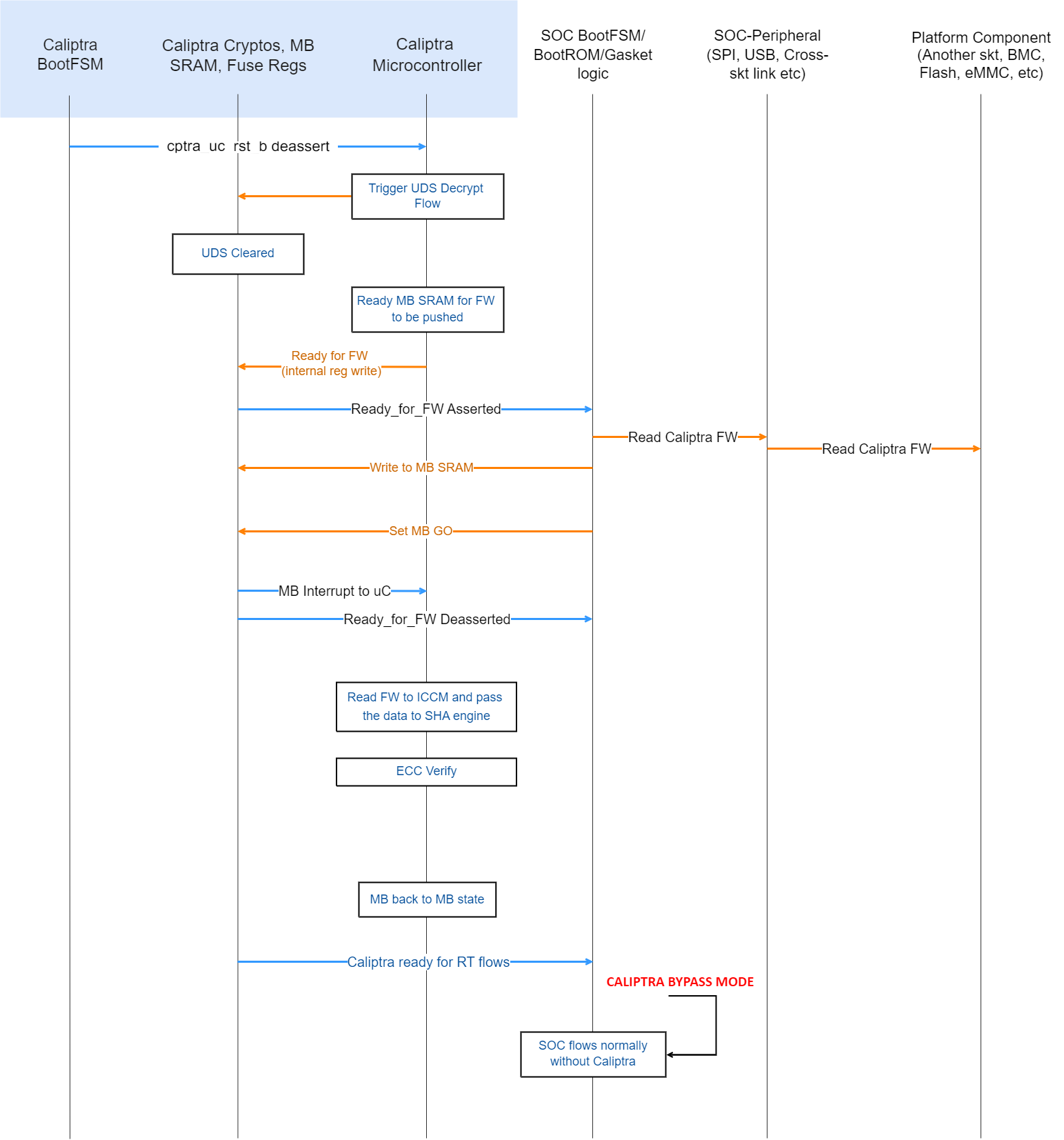
- After the Caliptra microcontroller is out of reset, ROM starts executing and triggers the crypto block to run the UDS decrypt flow.
- Caliptra ROM enables the mailbox. (Until this point, any accidental or non-accidental writes that target the mailbox are dropped by the hardware.)
- Caliptra ROM asserts READY_FOR_FW wire. This is done by writing an internal register. This register is also visible to read on the AXI interface. SoC can choose to poll on this bit instead of using the wire (it is the SoC integration choice).
- SoC follows the mailbox protocol and pushes Caliptra FW into the mailbox.
- Caliptra’s mailbox HW asserts an interrupt to the microcontroller after the GO is written, per mailbox protocol. See Mailbox for specifics.
- After Caliptra’s FW is authenticated and loaded into ICCM, microcontroller runs the firmware and asserts READY_FOR_RTFLOWS wire.
Subsystem FW Load flow for Subsystem Mode
Please see the subsystem architecture section below.
CPU warm reset or PCIe hot reset flow → Caliptra IP reset
Figure 11: Hardware reset flow
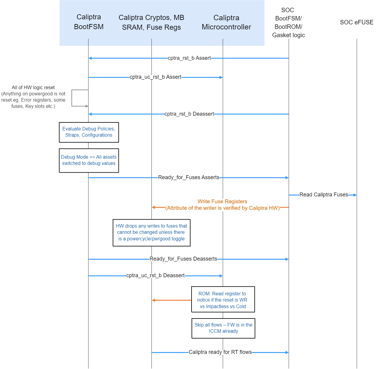
Note: Since Caliptra IP may be placed in an ACPI S5 domain of the device, there may be devices where Caliptra IP may not go through reset on a device hot reset or CPU warm reset. But the flow shows what happens when such a reset happens.
- Caliptra IP’s reset is asserted by the SoC.
- Caliptra’s internal BootFSM resets the microcontroller and then resets all of the logic (including the SoC-facing AXI interface). Only registers or flops that are sitting on powergood are left with the same value. Note that SRAMs do not have a reset.
- Caliptra IP’s reset is deasserted by the SoC.
- At this point, the HW boot flow is the same as the cold boot flow. SoC is required to configure the internal TRNG and ROM WDT and then set CPTRA_FUSE_WR_DONE. This causes Caliptra IP to deassert the Ready_for_Fuse wire.
- Caliptra’s ROM reads an internal register to differentiate between warm, cold, and impactless flow. If it's a warm reset flow, then it skips DICE key generation and FW load flows (because keys were already derived and FW is already present in ICCM). This is an important reset time optimization for devices that need to meet the hot reset specification time.
Because warm reset is a pin input to Caliptra, Caliptra may not be idle when a warm reset occurs. If a warm reset occurs while Caliptra ROM, FMC, or RT initialization code is executing, Caliptra may be inoperable until a subsequent cold reset. If a warm reset occurs while Caliptra runtime is servicing a request, Caliptra shall remain operable but may refuse to wield production assets for subsequent requests.
Note: The cold reset flow is not explicitly mentioned but it is the same as the cold boot flow because Caliptra IP has no state through a cold reset. Note: Subsystem mode's warm reset flow is the same as above, except the warm reset action is triggered/managed by MCU.
Random Number Generator
TRNG is the digital logic and algorithms that are required for random number generation. It requires a physical entropy source input. See the Caliptra hardware specification and integration specification here for more information on the implementation and connectivity of TRNG.
- For SoCs that want to use their own legacy TRNG, Caliptra provides a HW API to push the random number on the request/response handshake. Details on this are also available in the Caliptra hardware specification and integration specification. This mode is advised for early development but discouraged for production tape outs due to the lower security assurances of an external TRNG.
- In Subsystem mode, Caliptra integrators are required to use the internal TRNG.
Mailbox
The Caliptra Mailbox is a 128 KiB buffer that is used to exchange data between the SoC and the Caliptra microcontroller.
The SoC communicates with the mailbox over an AXI interface. This allows the SoC to identify the device that is using the interface. This ensures that the mailbox, control registers, and fuses are read or written only by the appropriate device.
When a mailbox is populated by SoC, an interrupt to the FW occurs. This indicates that a command is available in the mailbox. The microcontroller is responsible for reading from and responding to the command.
When a mailbox is populated by the microcontroller, Caliptra sends a wire indication to the SoC that a command is available in the mailbox as well as updating the MAILBOX STATUS register. The SoC is responsible for reading from and responding to the command.
Mailboxes are generic data passing structures, and the Caliptra hardware only enforces the protocol for writing to and reading from the mailbox. How the command and data are interpreted by the FW and SoC are not enforced in Caliptra.
Sender protocol
Sending data to the mailbox:
- Requester queries the mailbox by reading the LOCK control register.
- If LOCK returns 0, LOCK is granted and is set to 1.
- If LOCK returns 1, MBOX is locked for another device.
- Requester writes the command to the COMMAND register.
- Requester writes the data length in bytes to the DLEN register.
- Requester writes data packets to the MBOX DATAIN register.
- Requester writes to the EXECUTE register.
- Requester reads the STATUS register until a value other than CMD_BUSY is detected. This is also indicated by a dedicated wire that asserts when STATUS is changed. STATUS can return:
- DATA_READY – Indicates the return data is in the mailbox for the requested command.
- CMD_COMPLETE – Indicates the successful completion of the requested command.
- CMD_FAILURE – Indicates the requested command failed.
- CMD_BUSY – Indicates the requested command is still in progress.
- If response data is expected and the requester reads a STATUS of DATA_READY:
- Requester reads from the DLEN register to ascertain the size of the response data.
- Requester reads data from the DATAOUT register until DLEN bytes are read.
- After reading the response data, if any, requester writes 0 to the EXECUTE register to clear LOCK.
Notes on behavior: After LOCK is granted, the mailbox is locked until that device has concluded its operation. The mailbox is responsible only for accepting writes from the device that requested and locked the mailbox.
Figure 12: Mailbox sender flow
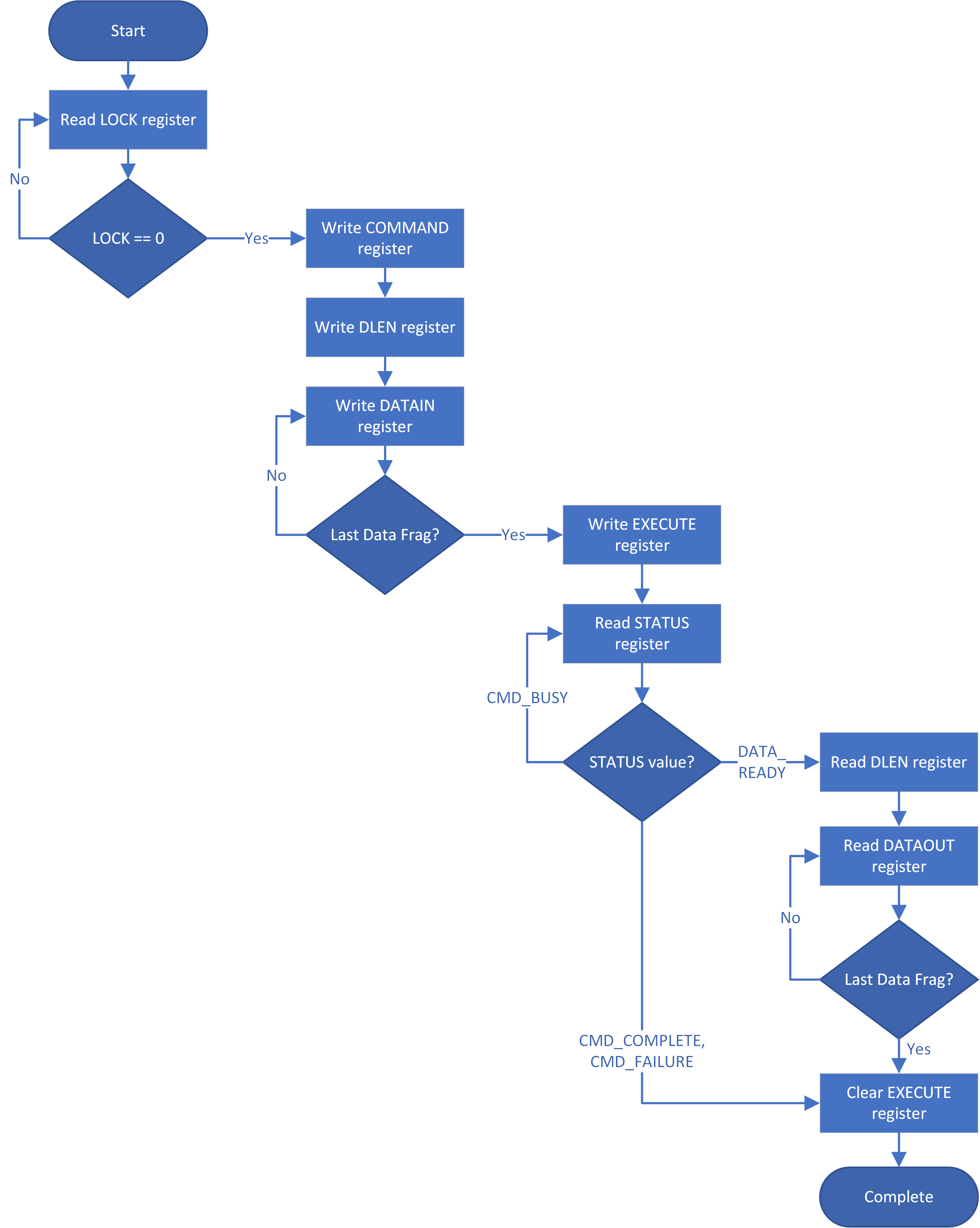
Receiver protocol
Upon receiving an indication that the mailbox is populated, the appropriate device can read the mailbox. This is indicated by a dedicated wire that is asserted when Caliptra populates the mailbox for SoC consumption.
Receiving data from the mailbox:
- Receiver reads the COMMAND register.
- Receiver reads the DLEN register.
- Receiver reads the MBOX DATAOUT register.
- Continues reading MBOX DATAOUT register until DLEN bytes are read.
- If response data is required:
- Receiver writes the size of the response data to the DLEN register.
- Receiver writes to the DATAIN register until DLEN bytes are written.
- Note: Response data is only supported for Caliptra, to SoC-initiated commands. SoC cannot provide response data for Caliptra-initiated commands.
- Receiver writes to the STATUS register.
- If response data was provided, STATUS should be written to DATA_READY.
- Otherwise, STATUS should be written to CMD_COMPLETE (or CMD_FAILURE).
Figure 13: Mailbox receiver flow
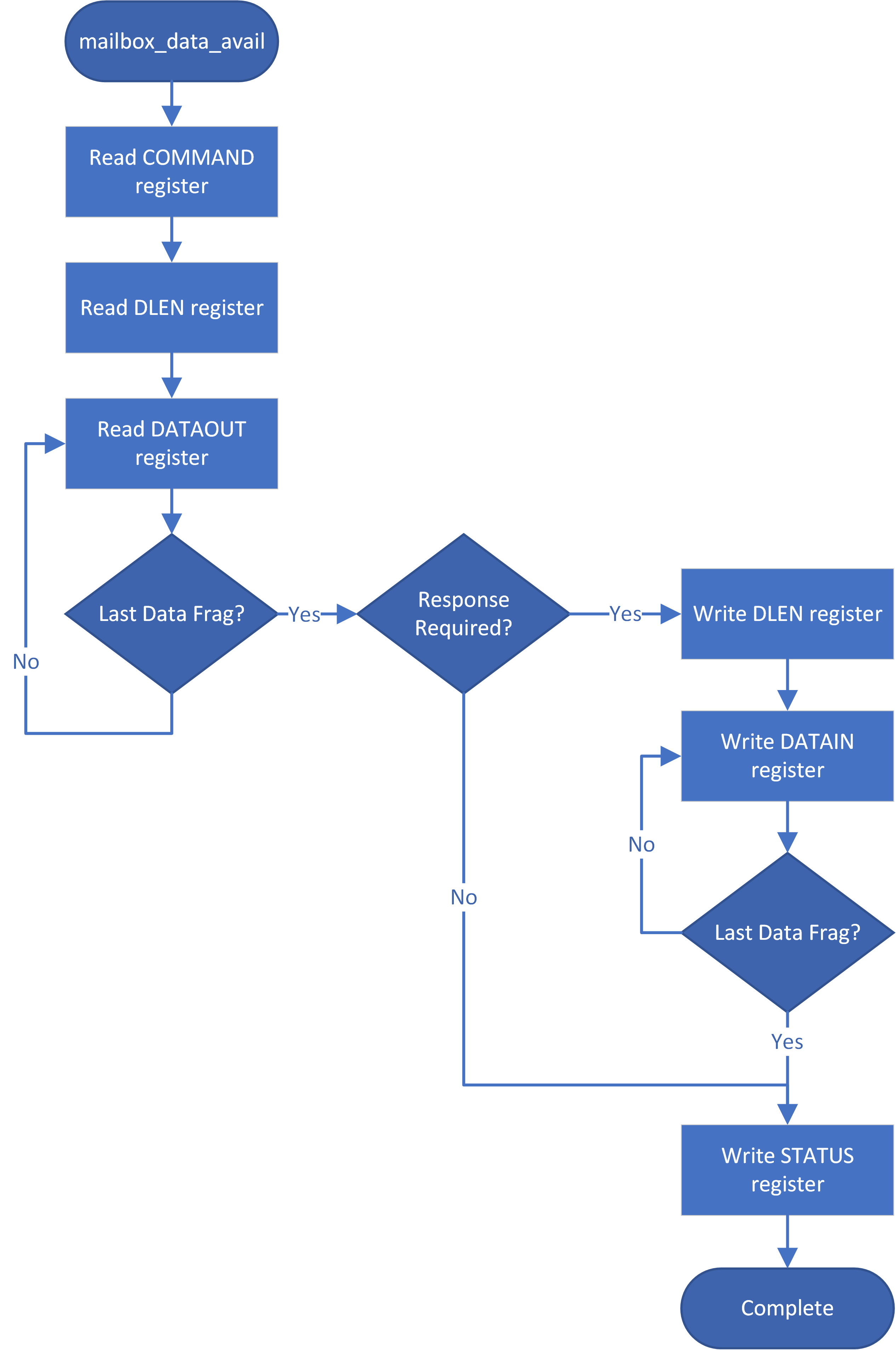
User attributes
The AXI_USER field of the AXI interface is used to encode device attributes for the requester that is utilizing the SoC interface. These values can be used for:
- Ensuring the device that was granted the LOCK is the one that accesses the MBOX, DLEN, COMMAND, and STATUS registers.
- Prioritizing who is next granted the LOCK.
- Mailbox user 0xFFFF_FFFF is reserved for Caliptra internal use. Caliptra firmware will fail any SoC requests from this user.
Mailbox commands
The Caliptra mailbox commands are specified in the Caliptra runtime firmware specification.
Cryptographic mailbox commands
Cryptographic mailbox (CM) commands are a flexible set of mailbox commands that provide access to Caliptra's cryptographic cabilities. This is meant for key storage and use to support protocols like SPDM and OCP LOCK.
These commands are not meant to be high-performance as they are accessed via mailbox commands.
Key material and data will be stored in an encrypted and authenticated section of DCCM. Keys are used via handles that refer to portions of DCCM.
These mailbox commands extend Caliptra's cryptographic support to include SHA, HMAC, HKDF, AES, ECDH, ML-KEM, and RNG services in addition ECDSA and ML-DSA.
The runtime firmware specification contains further details.
Hash calculation HW API (Subsystem mode only)
Caliptra provides a HW API to do a SHA384 hash calculation. The SoC can access the accelerator through the Caliptra FW API only in subsystem mode. Caliptra FW API uses the internal SHA accelerator and its DMA widget be hash the required data and present it back to Calitpra FW.
JTAG/TAP debug
Figure 14: Debug flow
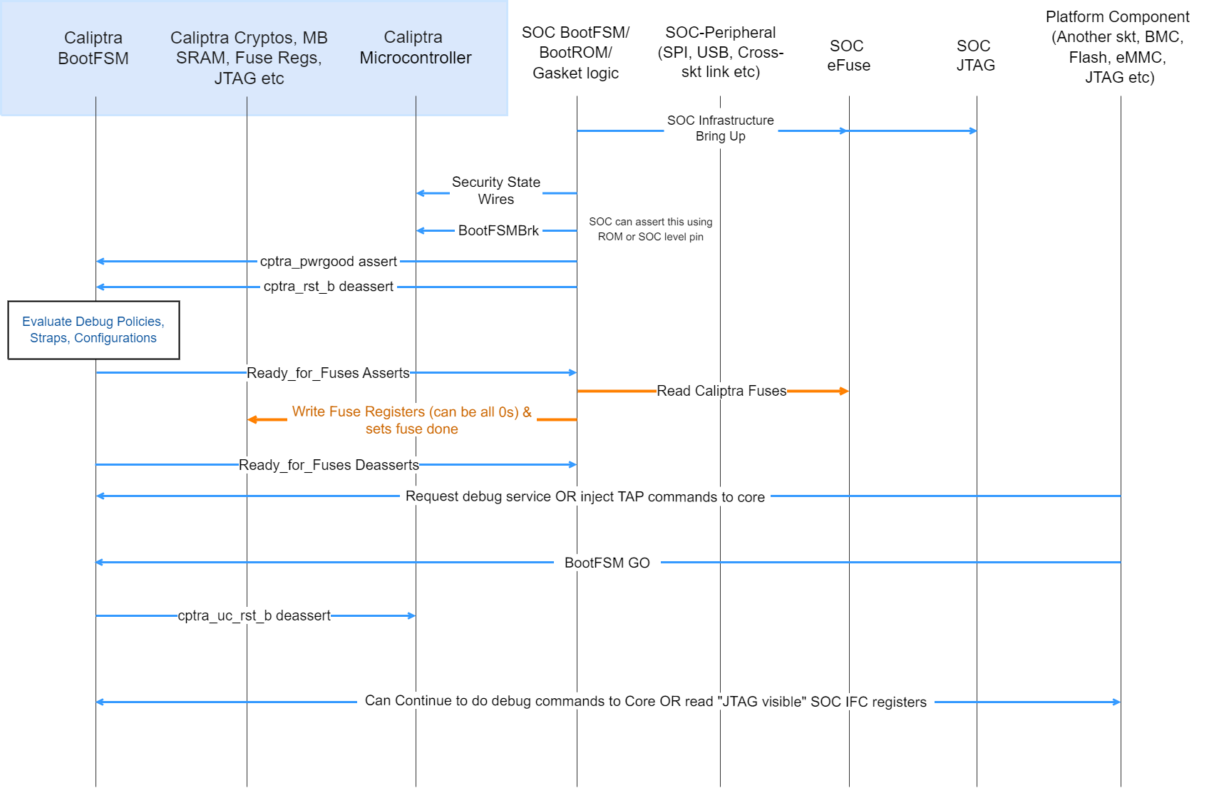
- SoC drives the security state indicating that it is a debug flow. See Caliptra security states for encodings.
- SoC (using a GPIO pin or SoC ROM) drives BootFSMBrk (this is also used for debug cases). This can be driven at any time before cptra_rst_b is deasserted.
- SoC follows the boot flow as defined in Caliptra IP HW boot flow to assert cptra_pwrgood and deassert cptra_rst_b, followed by writing to the fuse registers.
- HVM, through JTAG or through the Caliptra SoC interface, writes to “CPTRA_DBG_MANUF_SERVICE_REG”, requesting the appropriate debug service (see the ROM/Runtime specifications for bit definitions).
- HVM, through JTAG, can also inject microcontroller TAP commands at this point following the VeeR Specification.
- HVM, through JTAG or through the Caliptra SoC interface, writes to “CPTRA_BOOTFSM_GO” to allow Caliptra’s internal BootFSM to continue to bring up microcontroller out of reset.
- Microcontroller executes the appropriate debug service.
- Specific SoC interface registers are accessible over the JTAG interface in debug (or manufacturing mode). The following are the JTAG register addresses for these registers.
Table 20: JTAG accessible registers
| Register name | JTAG address | Accessibility |
|---|---|---|
| MBOX_LOCK | 7'h75 | RO |
| MBOX_CMD | 7'h76 | RW |
| MBOX_DLEN | 7'h50 | RW |
| MBOX_DOUT | 7'h51 | RO |
| MBOX_DIN | 7'h62 | WO |
| MBOX_STATUS | 7'h52 | RW |
| MBOX_EXECUTE | 7'h77 | WO |
| BOOT_STATUS | 7'h53 | RO |
| CPTRA_HW_ERRROR_ENC | 7'h54 | RO |
| CPTRA_FW_ERROR_ENC | 7'h55 | RO |
| SS_UDS_SEED_BASE_ADDR_L | 7'h56 | RO |
| SS_UDS_SEED_BASE_ADDR_H | 7'h57 | RO |
| HW_FATAL_ERROR | 7'h58 | RO |
| FW_FATAL_ERROR | 7'h59 | RO |
| HW_NON_FATAL_ERROR | 7'h5a | RO |
| FW_NON_FATAL_ERROR | 7'h5b | RO |
| CPTRA_DBG_MANUF_SERVICE_REG | 7'h60 | RW |
| BOOTFSM_GO | 7'h61 | RW |
| SS_DEBUG_INTENT | 7'h63 | RW |
| SS_CALIPTRA_BASE_ADDR_L | 7'h64 | RW |
| SS_CALIPTRA_BASE_ADDR_H | 7'h65 | RW |
| SS_MCI_BASE_ADDR_L | 7'h66 | RW |
| SS_MCI_BASE_ADDR_H | 7'h67 | RW |
| SS_RECOVERY_IFC_BASE_ADDR_L | 7'h68 | RW |
| SS_RECOVERY_IFC_BASE_ADDR_H | 7'h69 | RW |
| SS_OTP_FC_BASE_ADDR_L | 7'h6A | RW |
| SS_OTP_FC_BASE_ADDR_H | 7'h6B | RW |
| SS_STRAP_GENERIC_0 | 7'h6C | RW |
| SS_STRAP_GENERIC_1 | 7'h6D | RW |
| SS_STRAP_GENERIC_2 | 7'h6E | RW |
| SS_STRAP_GENERIC_3 | 7'h6F | RW |
| SS_DBG_MANUF_SERVICE_REG_REQ | 7'h70 | RW |
| SS_DBG_MANUF_SERVICE_REG_RSP | 7'h71 | RW |
| SS_DBG_UNLOCK_LEVEL0 | 7'h72 | RW |
| SS_DBG_UNLOCK_LEVEL1 | 7'h73 | RW |
| SS_STRAP_CALIPTRA_DMA_AXI_USER | 7'h74 | RW |
Note: These are injected as TAP register read/write commands as defined in the VeeR Specification.
Notes:
- The security state is latched at cptra_rst_b deassertion. If the security state is unlocked at this time, only TAP is opened.
- Changing the security state at a random time after cptra_rst_b deassertion (Caliptra in passive mode): does not unlock Caliptra JTAG.
- Changing the security state at a random time after cptra_rst_b deassertion (Caliptra in passive mode): transition from debug locked to debug unlocked has no effect until next reset.
- Changing the security state at a random time after cptra_rst_b deassertion (Caliptra in subsystem mode): Refer to Production Debug Unlock Architecture for details of the full procedure.
- Setting scan mode at a random time after cptra_pwrgood: flushes out all internal Caliptra secrets, assets, key vault, and crypto intermediate state.
- Scan mode assertion does not automatically open Caliptra JTAG.
Architectural registers
These registers are accessible over AXI to be read according to the register access permissions. For more information, see the register reference manual at https://ereg.caliptra.org.
Fuse requirements
Fuse registers are programmable whenever IP goes through reset (after cptra_rst_b asserts and de-asserts) and before the fuse registers are locked from writes. If the lock was set, the writes are dropped. The lock is sticky across a warm reset.
To ensure that the security claims of Caliptra are achieved, specific fuse protection capabilities must be supported:
- Fuses that hold Caliptra secrets shall not be readable by any mutable code in the SoC. The intent is to provide defense-in-depth for the UDS.
- For SoCs that intend to achieve FIPS 140-3 CMVP certification with Caliptra, SoC shall implement a HW state machine for copying the uds_seed, field_entropy, and key_manifest_pk_hash fuses from the fuse controller into Caliptra's fuse shadow registers. Only the fuse controller, this state machine, and Caliptra shall be able to access these fuse values. The intent is to not include the SoC ROM as part of the cryptographic module boundary.
- For the production lifecycle state, if JTAG is enabled pre or post SoC reset, then Caliptra's dedicated fuses shall not be accessible (shall not be readable, shall not be writable) by Caliptra or other SoC IP. This restriction shall be applicable to Caliptra's fuse shadow registers as well (see Physical Attack Countermeasures).
- SoC should ensure that the integrity of each fuse is maintained through the life of the part. The integrity of the fuses can be maintained by fuse redundancy, ECC, or other means determined sufficient by the SoC.
Fuse programming
All fuse based cryptographic keying material and seeds (for example, UDS Seed) shall be generated (on-chip or off-chip) per requirements described in Reference 8.
SoC shall support in-field programmable fusing. Fuse Map shows which fuses are expected to be in-field programmable. SoCs shall implement authorization for in-field programmable fusing to mitigate denial-of-service attacks. Authorization design is outside the scope of this specification. In Subsystem mode, SoC may use MCU RT FW for these actions.
SoC shall support a field entropy programming API. The API shall support retrieving an input value from an external interface. It should cryptographically mix that value with the output of an on-die TRNG to generate the field entropy value. The API implementation shall burn the field entropy value into the first available field entropy fuse slot (or fail if no slots are available). Caliptra is expected to be in any security state. The device owner is expected to call this API in a “clean room environment” to minimize risk of attack on the programming process. In Subsystem mode, SoC may use MCU RT FW for these actions.
Fuse zeroing
Caliptra assumes that the unfused value in fuses is '0' and the fused value is '1'. With this context, zeroization refers to destroying a secret value by fusing it to all ones.
For SoCs that intend to achieve FIPS 140-3 CMVP certification with Caliptra:
- SoC shall implement zeroization for uds_seed and field_entropy such that the fuse rows holding these secrets contain all ones.
- SoC shall expose and document an API for a tester to invoke zeroization.
- SoC shall indicate that zeroization has occurred by statically asserting GENERIC_INPUT_WIRE[0] to Caliptra.
- SoC shall set Caliptra’s security state to DebugUnlock by ORing it with the zeroization status signal.
- SoC shall expose Caliptra architectural registers as API for a tester to read.
- SoC shall ensure authorization for this API to guard against denial-of-service attacks.
- Note: In Subsystem mode: SoC should use MCU ROM with the corresponding subsystem HW components for these actions. Authorization is handled via the PPD pin.
Fuse map
FIXME: Needs updates for Caliptra 2p0 & Subsystem The following table describes Caliptra's fuse map:
Table 21: Caliptra Fuse Map
| Name | Size (bits) | ACL | Fuse programming time | Description |
|---|---|---|---|---|
| UDS SEED (obfuscated) | 512 | ROM | SoC manufacturing | DICE Unique Device Secret Seed. This seed is unique per device. The seed is scrambled using an obfuscation function. |
| FIELD ENTROPY (obfuscated) | 256 | ROM | Device owner in-field programmable | Field-programmable by the owner, used to hedge against UDS disclosure in the supply chain. |
| VENDOR PK HASH | 384 | ROM FMC RUNTIME | SoC manufacturing | SHA384 hash of the Vendor ECDSA P384 and LMS or MLDSA Public Key Descriptors. |
| ECC REVOCATION | 4 | ROM FMC RUNTIME | In-field programmable | One-hot encoded list of revoked Vendor ECDSA P384 Public Keys (up to 4 keys). |
| OWNER PK HASH | 384 | ROM FMC RUNTIME | In-field programmable | SHA384 hash of the Owner ECDSA P384 and LMS or MLDSA Public Keys. |
| FMC KEY MANIFEST SVN | 32 | ROM FMC RUNTIME | In-field programmable | FMC security version number. (Deprecated in 2.0, will be removed in a future RTL revision.) |
| RUNTIME SVN | 128 | ROM FMC RUNTIME | In-field programmable | Firmware security version number. |
| ANTI-ROLLBACK DISABLE | 1 | ROM FMC RUNTIME | SoC manufacturing or in-field programmable | Disables anti-rollback support from Caliptra. (For example, if a Platform RoT is managing FW storage and anti-rollback protection external to the SoC.) |
| IDEVID CERT IDEVID ATTR | 768, 352 used | ROM FMC RUNTIME | SoC manufacturing | IDevID Certificate Generation Attributes. See IDevID certificate section. Caliptra only uses 352 bits. Integrator is not required to back the remaining 416 bits with physical fuses. |
| IDEVID MANUF HSM IDENTIFIER | 128, 0 used | ROM FMC RUNTIME | SoC manufacturing | Spare bits for Vendor IDevID provisioner CA identifiers. Caliptra does not use these bits. Integrator is not required to back these with physical fuses. |
| LIFE CYCLE | 2 | ROM FMC RUNTIME | SoC manufacturing | Caliptra Boot Media Integrated mode usage only. SoCs that build with a Boot Media Dependent profile don’t have to account for these fuses. - '00 - Unprovisioned - '01 - Manufacturing - '10 - Undefined - '11 - Production Reset: Can only be reset on powergood. |
| LMS REVOCATION | 32 | ROM | In-field programmable | One-hot encoded list of revoked Vendor LMS Public Keys (up to 32 keys). |
| MLDSA REVOCATION | 4 | ROM | In-field programmable | One-hot encoded list of revoked Vendor MLDSA Public Keys (up to 4 keys). |
| SOC STEPPING ID | 16 | ROM FMC RUNTIME | SoC manufacturing | Identifier assigned by vendor to differentiate silicon steppings. |
| MANUF_DEBUG_UNLOCK_TOKEN | 512 | ROM | SoC manufacturing | Digest value for manufacturing debug unlock token secret value for authorization. |
| PQC Key Type | 2 | ROM FMC RUNTIME | In-field programmable | One-hot encoded selection of PQC key type for firmware validation. - Bit 0 - MLDSA - Bit 1 - LMS |
| SOC MANIFEST SVN | 128 | ROM FMC RUNTIME | In-field programmable | One-hot encoded value for the SOC authorization manifest minimum supported SVN. |
| SOC MANIFEST MAX SVN | 8 | ROM FMC RUNTIME | In-field programmable | Maximum value for the SOC authorization manifest SVN. |
| HEK RATCHET SEED | 256 | ROM | In-field programmable | OCP L.O.C.K. seed used by hardware to generate HEK |
Error reporting and handling
This section describes Caliptra error reporting and handling.
Table 22: Hardware and firmware error types
| Fatal errors | Non-fatal errors | |
|---|---|---|
| Hardware | - ICCM, DCCM SRAM ECC. - The second watchdog (WD) timer expiry triggers an NMI, and a FATAL error is signaled to the SoC. - Operating HMAC, ECC, or DOE engines simultaneously. | - Mailbox SRAM ECC (except initial firmware load) - Mailbox incorrect protocol or commands. For example, incorrect access ordering or access without Lock. |
| Firmware | - Control Flow Integrity (CFI) errors. - KAT errors. - FIPS Self Test errors. - Mailbox commands received after FIPS Shutdown request completes. - Hand-off errors detected upon transfer of control from ROM to FMC or FMC to Runtime. - Mailbox protocol violations leading the mailbox to an inconsistent state if encountered by ROM during cold reset flow. - Firmware image verification or authentication failures if encountered by ROM during Cold Reset flow. - Non-aligned access to ICCM or DCCM - AHB access hangs, triggered through WD timer expiry - AHB access outside of the decoding range | - Firmware image verification or authentication failures if encountered by ROM during Update Reset flow. - Mailbox protocol violations leading the mailbox to an inconsistent state (if encountered by ROM during Update Reset flow). - Cryptography processing errors. |
Fatal errors
- Fatal errors log the FATAL ERROR reasons into an architectural register that is RW from the external world. This register must be sticky (as in, reset is on powergood).
- This register may be cleared at any time via register write (W1C).
- Caliptra signals fatal errors using a cptra_error_fatal wire.
- SoCs should connect this into their SoC error handling logic. Upon detection of a FATAL ERROR in Caliptra, SoC shall treat any outstanding commands with Caliptra as failed, and SoC may recover by performing a Caliptra reset using the signal
cptra_rst_b. - This signal prevents forward progress of the boot process if measurement submission to Caliptra fails. If SoC detects a Caliptra fatal error while the SoC is in steady state, then there is no obligation for the SoC to immediately address that error. If rebooting the SoC for such failures is deemed unacceptable to uptime, the SoC should implement the ability to trigger a Caliptra warm reset independently of the SoC, and may use this mechanism to recover.
- Error mask registers (writable only by Caliptra microcontroller) may be used to prevent error signal assertion per-event. Mask registers only impact interrupts when they are set prior to the error occurrence.
- cptra_error_fatal remains asserted until Caliptra is reset. Note that, although the HW FATAL ERROR register fields may be cleared at any time, a reset is still required to clear the interrupt.
- SoCs should connect this into their SoC error handling logic. Upon detection of a FATAL ERROR in Caliptra, SoC shall treat any outstanding commands with Caliptra as failed, and SoC may recover by performing a Caliptra reset using the signal
- When a fatal error occurs, all volatile assets that are stored in key vault are cleared.
Non-fatal errors
- Non-fatal errors log the NON-FATAL ERROR reasons into an architectural register that is RW from the external world. This register must be sticky (as in, reset is on powergood).
- This register may be cleared at any time via register write (W1C).
- Caliptra signals non-fatal errors using a cptra_error_non_fatal wire.
- Caliptra reset via
cptra_rst_b, or a write to clear the NON-FATAL ERROR register, cause the interrupt to deassert. - It is optional for SoCs to include this signal in their logic.
Firmware errors
Please refer to the Caliptra code base for a list of the error codes.
Caliptra Security Subsystem
The Caliptra subsystem offers a complete RoT subsystem, with open source programmable components for customization of SoC boot flows.
Figure: Caliptra security subsystem
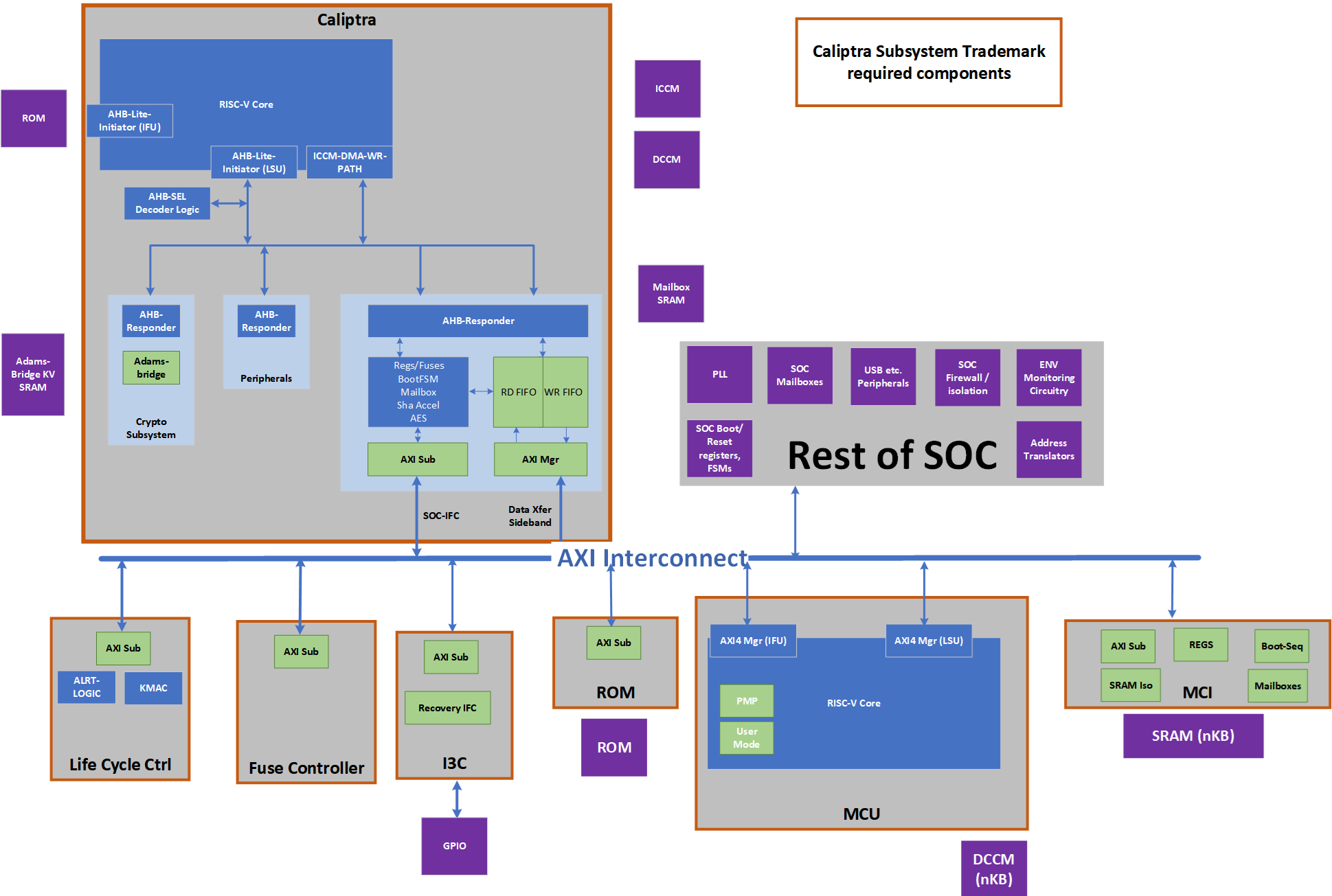
Caliptra Subsystem Trademark Compliance
- Caliptra subsystem trademark compliance shall have Caliptra Core 2.0, Life Cycle Controller, Fuse Controller, I3C with OCP streaming boot interface, Manufacture Control Unit (MCU) and Manufacturer Control Interface (MCI) taken as is without change to ensure there is hardware transparency and consistency.
- Caliptra subsystem provides life cycle state to the SoC.
SoC Integration Flexibility
- SoC may choose to add PLLs (Phase Locked Loop for stable clock generation), SoC specific mailboxes, SoC specific firewalls & address translations, environmental circuitry as some examples.
- Caliptra subsystem provides flexibility to SoC to remap subsystem driven debug levels to SoC specific debug policies.
- Please see Subsystem hardware and integration specifications for additional details on subsystem configurability (FIXME: Add md versions once available; right now they are uploaded as pdfs in Caliptra-SS repository's doc folder).
Caliptra Subsystem Architectural Flows
Subsystem (Pre-FW Load) Boot Flow
Note: Any step done by MCU HW/ROM would have been performed by “SoC Manager” in Caliptra 1p0.
- SoC (using its HW or MCU ROM) performs pre-steps like bringing up CRO or PLL, MBIST flows on SRAMs, SRAM Init etc.
- SoC will assert MCU & Caliptra pwrgood and after 10 cycles MCU
- MCU ROM or SoC Manager wrapper will bring up fuse controller and any other SoC specific infrastructure RTL modules (I3C, GPIO programming, Glitch detector programming etc.)
- MCU ROM or SoC Manager wrapper will deassert Caliptra reset.
- Caliptra HW will read the security centric (secret) fuses.
- MCU ROM waits for ready_for_fuses to be asserted.
- MCU ROM or SoC Manager will populate the remaining fuses of Caliptra and reads its own fuses (if any). Note that this step is gated behind the completion of security fuse writes to ensure the step has completed.
- MCU ROM will write “fuse done” to Caliptra.
- Caliptra will go through its boot flow of bringing up uC.
- Caliptra ROM starts and executes various KATs flows.
Subsystem Boot Flow
If (Caliptra-Passive-Mode)
- SoC Manager goes through Caliptra 1.x flows => loads Caliptra FW using Caliptra 1.x flows, Caliptra sets RT ready and SOC <-> Caliptra boot flow is done.
(Caliptra-Subsystem-Mode)
- Caliptra ROM waits for SoC infrastructure readiness indication. If this indication is set, Caliptra will do the identity derviation flows. If it is not set, then this flow is run when the SoC infrastructure readiness indication is set.
- Caliptra ROM uses the streaming boot interface to load its firmware. Please see the specific section for next level specifics; At a high level, Caliptra ROM sets the device ready in the I3C controller and poll I3C for the payloads.
- BMC or a similar platform component will send the image (code or data) through OCP streaming boot interface. 1.Caliptra ROM uses the streaming boot interface to receive 'data' from the BMC or MCU. Examples include SoC specific configuration. Caliptra ROM operation of the streaming boot interface will be identical for receiving either 'code' or 'data'. The data flow and code flow over streaming boot interface is the same from physical interface point of view and follows the OCP recovery spec for streaming boot support as implemented in Caliptra subsystem documentation (please see the recovery section). 2. This need for data flow (from flash or BMC) is indicated by a SOC configuration bit to Caliptra ROM. 3. This ‘data’ flow is possible only before SOC infra readiness is set. This is specifically used for scenarios where PUF or other characterization data is coming off-chip (say a flash or BMC). FIXME: Security and operations impact of this step/flow is being analyzed. This capability/flexibility will be updated or removed once that is finalized. 4. This data must be hashed into PCR0 5. To keep the scope limited, only one ‘data’ flow is allowed
- If the data was required to be run (is indicated by a SOC configuration bit to Caliptra ROM), Caliptra ROM waits for SOC infrastructure readiness to be set. Once set, it will do the required key derivations.
- Caliptra ROM will read the streaming boot interface registers (data payload registers) over AXI manager interface and write into Caliptra MB SRAM. The offset of the streaming boot interface registers are available through a config register that is set at SOC integration time or by MCU ROM.
- Note that an intelligent I3C peripheral could “stream” the image. This is a future enhancement.
- Caliptra ROM will authenticate its image sitting in Caliptra MB SRAM
- Caliptra ROM flow will be similar to Caliptra 1.0 flow with PQC FW Authentication.
- Caliptra ROM will derive required keys similar to Caliptra 1.0 flow (while accounting for PQC)
- Caliptra ROM will switch to RT image.
- Caliptra RT FW will set the Streaming boot interface to allow BMC’s Recovery Agent (RA) to send the next image (which MUST be SOC image manifest).
- BMC RA is required to know the different component of the images using the similar manifestation as DSP0267 PLDM for Firmware Update over MCTP components.
- Caliptra RT FW will read the Streaming boot interface registers over AXI manager interface and write the image to its mailbox.
- Caliptra RT FW will authenticate SoC manifest using the keys available through Caliptra Image, authenticate the image, capture the measurement and capture the relevant information into DCCM.
- Caliptra RT FW will set the Streaming boot interface to allow BMC’s Recovery Agent (RA) to send the next image (which MUST be MCU image manifest).
- BMC RA is required to know the different component of the images using the similar manifestation as DSP0267 PLDM for Firmware Update over MCTP components.
- Caliptra RT FW will read the Streaming boot interface registers over AXI manager interface and write the image to MCU SRAM aperture (that is open to Caliptra only by HW construction).
- The address of the MCU SRAM is provided to Caliptra’s RT FW through SOC manifest.
- Note: From validation front, need to ensure the Caliptra ROM and MCU are aligned in endianness.
- Caliptra RT FW will instruct Caliptra HW to read MCU SRAM and generate the hash (Caliptra HW will use the SHA accelerator and AXI mastering capabilities to do this)
Open: Should we have a capability to do something like this for decryption too? (Key to be provided by MCU/SOC before running the decryption flow?)
- Caliptra RT FW will use this hash and verify it against the hash in the SOC manifest.
- Caliptra RT FW after verifying/authorizing the image and if it passes, it will set EXEC/GO bit into the register as specified in the previous command. This register write will also assert a Caliptra interface wire.
- MCU ROM will be polling the breadcrumb that the MCU SRAM has valid content and will jump to the MCU SRAM to execute from it. NOTE: This breadcrumb should be one of the status bits available on the MCU interface that is set by Caliptra GO bit wires.
- Until this step MCU SRAM aperture that holds the MCU RT FW and certain Streaming boot interface registers are not accessible to MCU.
- MCU RT FW will now set Streaming boot flow is completed.
- BMC or a similar platform component will now do MCTP enumeration flow to MCU over I3C.
- MCU RT FW is responsible for responding to all MCTP requests.
- MCU RT FW will do the PLDM T5 flow, extract FW or configuration payload, use Caliptra to authenticate and deploy the rest of the images as described in run-time authentication flows.
Figure: Subsystem Boot Flow
Common Run-time Authentication Flows
- MCU RT FW will do PLDM T5 flow to obtain the FW images for downstream uControllers (or other SoC configuration)
- MCU RT FW will send/stream the (FW or config) payload to Caliptra SHA Acc to perform hash measurements as the payload comes through the MCTP transport.
- MCU RT FW can either stage the entire image or write to the final destination as a part of the previous step depending on the SOC construction.
- Note: By SOC security/design construction, the FW/payload that is loaded must NOT be allowed to execute or be used until Caliptra authorizes that the FW/payload.
- MCU RT FW will issue the imageID & GO-field bit (bit that Caliptra RT FW would set if the image authorization is successful) to Caliptra RT FW to start off the process of image authorization of the image that was hashed.
- Caliptra RT FW will obtain this hash from the internal SHA accelerator register that was used to hash in the previous step.
- Caliptra RT FW after verifying/authorizing the image and if it passes, it will set EXEC/GO bit into the register as specified in the previous command. This register write will also assert a Caliptra interface wire.
- MCU RT FW has an option of looking at the Mailbox command success or read the register or use the wire that the register will drive to allow the execution of the FW. This wire allows SOCs to construct a hardened logic of allowing executions from ICCM/TCMs only after the wire is set.
- SOC construction outside of MCU SRAM is SOC specific construction and the spec here provides recommendations on using MCU and Caliptra to build such a logic. Please refer to Caliptra subsystem hardware specification for construction specifics (Hint: These functions are integrated into Manufacturer Control Interface [MCI]).
- Any logic outside of the Caliptra Subsystem boundary is SoC specific and will be custom to the SoC design. This specification provides recommendations for how Caliptra and MCU may be integrated into the SoC.
FIXME: Add the visio flow picture
Subsystem support for Hitless Updates
Caliptra Hitless Update
- Payloads of all hitless update come over DSP0267 PLDM for Firmware Update over MCTP flow to the MCU similar to the boot time flows.
- MCU provides SOC manifest to Caliptra and waits for authentication to be successful. If this wasn’t provided Caliptra will use the latest SOC manifest available.
- If failed, MCU uses DSP0267 PLDM for Firmware Update over MCTP to report the same to the update agent using PLDM protocol
- MCU provides the Caliptra FW using Caliptra Mailbox using the hitless update flows documented in the Caliptra specification
MCU Hitless Update
- Payloads of all hitless update come over DSP0267 PLDM for Firmware Update over MCTP flow to the MCU similar to the boot time flows.
- MCU provides SOC manifest to Caliptra and waits for authentication to be successful. If this wasn’t provided Caliptra will use the latest SOC manifest available.
- If failed, MCU uses DSP0267 PLDM for Firmware Update over MCTP to report the same to the update agent using PLDM protocol
- MCU stages the incoming FW payload in an SOC-defined staging SRAM and provides the MMIO address of the staging memory to Caliptra. It is better to keep this as a part of the authenticated SOC manifest (as a configuration) from a security perspective.
- Caliptra RT FW will use the Caliptra DMA engine to issue the read and hash the image (note that the length of the image must be part of the SOC manifest)
- Caliptra RT FW after verifying/authorizing the image and if it passes, waits for activate command to be issued from MCU. MCU will get this command over DSP0267 PLDM for Firmware Update over MCTP flow; At this point, Caliptra will reset EXEC/GO bit into the register as specified in the previous command. This register write will also deassert a Caliptra interface wire.
- MCU HW logic will use this indication to initiate MCU uC reset flow
- MCU HW logic sends a reset-go-req to MCU uC (an interrupt)
- MCU HW logic waits for reset-go-ack from MCU uC (Note that this handshake exists to ensure uController is in an appropriate quiescent state to take the reset)
- MCU HW logic will assert the reset to the MCU uC
- Caliptra RT FW will wait for reset assertion and then read the staged SRAM over AXI manager interface and write the image to the MCU SRAM aperture (that is open to Caliptra only by HW construction).
- The address of the MCU SRAM is provided to Caliptra’s RT FW through SOC manifest.
- Note: From the validation front, need to ensure the Caliptra ROM and MCU are aligned in endianness.
- Note: True downtime of MCU is from when its reset is asserted; It is SOC implementation requirement that it handles (eg. through buffering) all transactions to MCU while it is going through a hitless update.
- After the MCU SRAM is populated, Caliptra RT FW will set EXEC/GO bit into the register as specified in the previous command. This register write will also assert a Caliptra interface wire.
- MCU HW logic will use this indication to deassert the MCU reset.
- MCU ROM will look at the breadcrumb that the MCU SRAM has valid content and will start the execution from it directly. NOTE: This breadcrumb should be one of the status bits available on the MCU interface that is set by Caliptra GO bit wires.
SoC-FW Hitless Update
SoC may have other components that may need to be updated at run-time in a hitless/impactless manner.
The update flow will follow the same sequence as MCU Hitless update except they are executed by the MCU by using Caliptra as the RoT engine for doing all the required authentication/authorization flows.
Further SoCs may require the hitless update without impacting the workloads/VMs running on the host or the VMs using the devices. This essentially means that impactless update must happen without causing any timeouts to the in-flight transactions. While the treatment of those transactions are device dependent, Caliptra subsystem must provide a way to be able to authenticate and activate the FW in the shortest time possible.
Caliptra subsystem provides this architectural capability as follows:
- MCU provides SOC manifest to Caliptra and waits for authentication to be successful. If this wasn’t provided Caliptra will use the latest SOC manifest available.
- If failed, MCU uses DSP0267 PLDM for Firmware Update over MCTP to report the same to the update agent using PLDM protocol
- MCU stages all the incoming FW payload in an SOC-defined staging memory and provides the MMIO address of the staging SRAM to Caliptra. It is better to keep this as a part of the authenticated SOC manifest (as a configuration) from security perspective. (FW Arch requirement: This SOC-defined staging RAM MMIO offset which can be one for all the images or it could be per image, recommended to keep it the later way, should be defined in the SOC manifest.)
- Caliptra RT FW will use the Caliptra DMA engine to issue the read and hash the image (note that the length of the each image must be part of the SOC manifest)
- Caliptra RT FW will verify & authorize the images. It will also compare the hash of the images against the “current” hash of each of the image.
- MCU will send the ‘activate’ command to Caliptra (which is part of PLDM spec that MCU understands)
- If MCU FW is updated/new, Caliptra will execute the MCU Hitless update flow.
- Caliptra RT FW will then set the GO bits for all the SoC FWs that are updated (vs what was already running)
- SoC specific logic & MCU RT FW will use this information to update the remaining FW using SoC specific architectural flows. Note: Since this work is mainly distribution of the FW to the destination uCs, SoC should be built to do this flow as fast as possible to meet workload non-interruption/impactless requirements.
Multi-Chiplet Flows
This section explain how generic FW Load Flows would function for SoCs with multiple chiplets that are required to have their security controller functions. It is plausible that a SoC is built with a single security controller active on one chiplet and that serves all other chiplets.
Note: Additional control signals that MCU would control are SoC specific and are implemented through SoC widget(s).
- Primary tile uses Caliptra-Subsystem-Mode at its silicon boot time
- Secondary tile’s MCU ROM will go through the same common boot flow as the primary tile (except the peripheral could be inter-chiplet link).
- Secondary tile’s MCU ROM will wait for inter-chiplet link to be available for use (this would be an indication to MCU ROM)
- Primary tile’s MCU RT FW will fetch the secondary tile’s FW using DSP0267 PLDM for Firmware Update over MCTP T5 flow and ‘stream’ using the streaming boot interface protocol to the secondary tile(s).
- Based on SOC integration, inter-chiplet could be an intelligent peripheral that can DMA or implement data payload registers for Caliptra to read.
- Note that the indication from Caliptra for “next-image” follows the same streaming boot interface protocol.
- Note that to load the remaining images of a secondary tile, SOC can choose to do streaming boot flow for rest of the remaining images. Depending on the SOC architecture and chiplets, MCU RT FW may coordinate the SOC to boot in such a way that it “broadcasts” the same image to multiple chiplets that require the same image. This is a SOC optimized flow outside of Caliptra or Subsystem Context.
Caliptra Subsystem I3C Streaming Boot Interface
The streaming boot interface is implemented as an I3C target with commands defined by the OCP Recovery specification. It will have a unique address compared to any other I3C endpoint for the device. It will comply with I3C Basic v1.1.1 specification. It will support I3C read and write transfer operations. It must support Max read and write data transfer of 1-260B excluding the command code (1 Byte), length (2 Byte), and PEC (1 Byte), total 4 Byte I3C header. Therefore, max streaming boot data per transfer will be limited to 256-byte data.
I3C streaming boot interface is responsible for the following list of actions:
- Responding to command sent by Recovery Agent (RA)
- Updating status registers based on interaction of AC-RoT and other devices
- Asserting / Deasserting “payload_available” & “image_activated” signals
OCP Recovery Interface Hardware Specifications
- Reference specifications for streaming boot sequence,
Caliptra Subsystem Streaming Boot Interface Hardware
Please refer to Caliptra subsystem Hardware specification.
Caliptra Subsystem Streaming Boot Sequence
- MCU ROM initializes the
PROT_CAP,DEVICE_STATUS,DEVICE_ID, andHW_STATUSregisters. Any other I3C initialization settings must be confirmed against I3C core specification. - Caliptra ROM updates the
PROT_CAPregister to set "Flashless boot (From RESET)", "FIFO CMS Support", and "Push-C-Image Support". - To start streaming boot, Caliptra ROM updates the
DEVICE_STATUSregister to "Recovery mode - ready to accept recovery image” for Device status byte (for the first image only) and "Flashless/Streaming Boot (FSB)" for Recovery reason codes. - Caliptra ROM updates the
RECOVERY_STATUSregister to "Awaiting Recovery Image" for Device recovery status and "image index" for Recovery image index. - BMC or a similar platform component sends an
INDIRECT_FIFO_CTRLwrite command with Component Memory Space (CMS) set to 0x0, reset set to 0x1, and image size set to streaming boot image size. - BMC or a similar platform component sends an
INDIRECT_FIFO_DATAwrite command. I3C device shall return a NACK response for any transfer that would cause the Head Pointer to advance to equal the Tail Pointer. BMC can implement flow control through NACK responses or by monitoring the FIFO space remaining via the Head and Tail Pointers. - The I3C device keeps head and tail pointers along with FIFO status up to date in the
INDIRECT_FIFO_STATUSregister. I3C streaming boot interface HW waits for an update toINDIRECT_FIFO_DATAwith exactly 256 bytes of data or less if remaining image data is less than 256 bytes. BMC could send multiple commands toINDIRECT_FIFO_DATAregister to fill the FIFO, but it must be a multiple of 4 bytes. The I3C device indicates payload availability only if the FIFO is full (256 bytes) or if BMC writes to image activation byte inRECOVERY_CTRLregister. - If
INDIRECT_FIFO_DATAhas 256B available to read, I3C device indicates data availability via side channel implemented as wirepayload_availableto Caliptra. For more information, see Requirement for payload available signal Implementation. Caliptra HW latches this wire into the register for Caliptra ROM/firmware to read. - If
payload_availableis asserted for the first time, Caliptra ROM readsINDIRECT_FIFO_CTRL_IMG_SIZEfor the image size. For eachpayload_availableassertion including the first one, Caliptra ROM continues to read the image data from theINDIRECT_FIFO_DATAregister until it finishes reading the data count specified as the image size. - Steps 8 and 9 repeat until all the image bytes are pushed over I3C and it matches the image size initialized in the
INDIRECT_FIFO_CTRL_IMG_SIZEregister. - When all the image bytes are received, Caliptra ROM sets
DEVICE_STATUSto "Recovery Pending (waiting for activation)". During image authentication,DEVICE_STATUSregister field device status remains "Recovery Pending (waiting for activation)". - After the above steps, Caliptra ROM/Firmware waits for BMC to activate the image. Image activation is indicated to Caliptra via either of the following methods:
- Side channel
image_activatedsignal. For more information, see Requirement for image activation signal implementation. - Caliptra ROM polls on
RECOVERY_CTRLregister for image activation status.
- When the image is activated, Caliptra ROM updates
RECOVERY_STATUSto “Booting recovery image” and moves to image authentication. - Irrespective of success or failure from image authentication (step 15 or 16), Caliptra ROM clears the image activation status before updating
RECOVERY_STATUS&DEVICE_STATUSregisters. - If the image activation is successful, and another recovery image stage is expected, then Caliptra RT firmware shall increment the “Recovery image index” in
RECOVERY_STATUSregister and set theRECOVERY_STATUSto indicate “Awaiting recovery image” (0x1). If no other stages are expected, then Caliptra RT firmware shall set theRECOVERY_STATUSto “Recovery successful”. Also, Caliptra ROM/Caliptra RT must update theDEVICE_STATUSregister to indicate "Running Recovery Image". - If the image consumption fails for any reason (for example, image authentication failure), Caliptra ROM/firmware updates
RECOVERY_STATUSregister to indicate appropriate recovery status andDEVICE_STATUSregister to "Fatal Error (Recover Reason Code not populated)". - BMC or a similar platform component sends the next image as requested in the image index, upon observing “Awaiting recovery image” in
RECOVERY_STATUSregister, and Caliptra RT FW and I3C HW go through the same flow as above.
Streaming Boot Sequence notes
- ROM refers to I3C registers by offset, and any change to the offset results in ROM failure or unexpected behavior.
- SoC is responsible for booting the I3C Core by configuring clock frequency/sampling rate with the following registers and any other requirements specified in I3C core specifications.
- SoC is responsible for assigning static addresses to the I3C Core.
- Caliptra ROM/runtime firmware updates the
RECOVERY_STATUSwith the recovery image index.- For recovery image index:
0x0: Caliptra firmware0x1: SoC Manifest0x2: MCU firmware
- For recovery image index:
- SoC/MCU ROM sets the
HW_STATUSregister per recovery spec at any time based on SoC-specific conditions. - MCU ROM programs
DEVICE_IDregister value based on associated fuse values. - SoC/MCU ROM initializes the
PROT_CAP,DEVICE_ID, andDEVICE_STATUSregisters. - Caliptra ROM performs only read-modify-write (RMW) for updates to registers.
- I3C device must update FIFO size (1-256 Byte), Max transfer size and type of region (tie this to 0x1) to
INDIRECT_FIFO_STATUSregister, which could be read by BMC firmware to understand the size of the FIFO and max transfer size. - BMC is responsible for re-sending the transaction if it fails due to PEC error.
- ALL Caliptra ROM accesses to recovery interface are completed via DMA assist.
Requirement for Payload Available Signal Implementation
- Name:
payload_available - Type: 1 bit wire
- Source: Recovery Interface / I3C Core
- Destination: Caliptra core
Assertion
- The
payload_availablesignal must assert under either of the following conditions:- If the recovery FIFO indicates full (256 bytes).
- If the image activation status is asserted and the recovery FIFO indicates not empty for the last transfer.
De-assertion
- The
payload_availablesignal must reset if recovery FIFO indicates empty.
Requirement for Image Activation Signal Implementation
- Name:
image_activated - Type: 1 bit wire
- Source: Recovery Interface
- Destination: Caliptra core
Assertion
- The
image_activatedsignal must assert whenRECOVERY_CTRLregister byte 2 has value0xf(indicating image activation).
De-assertion
- The
image_activatedsignal must deassert when theRECOVERY_CTRLregister byte 2 has value0x0(indicating image activation is cleared).
Platform component requirements for recovery support
- The BMC, or a similar platform, should not send payload to streaming boot interface (/I3C target) device if
RECOVERY_CTRLregister has byte 2 indicating Image Activated. BMC must wait to clear the byte 2. (Streaming boot interface is responsible for clearing this byte by writing 1). - The BMC, or a similar platform, sends payload to I3C target device in chunks of 256 bytes (header (4B) + FW bytes(256B) as I3C target transfer) only, unless it is the last write for the image. Before sending the payload, it reads FIFO empty status from
INDIRECT_FIFO_STATUSregister. - After the last write for the image, the BMC, or a similar platform, activates the image.
Life Cycle Controller & SoC Debug Architecture
Please refer to Caliptra subsystem hardware specification.
OCP L.O.C.K. HW Architecture and Security Claims
Please refer to Caliptra and Caliptra subsystem hardware specification for HW implementation details and Key Vault (KV) rules.
Security Claims and Assumptions
- The OCP LOCK implementation employs NIST approved algorithms (e.g., AES, SHA‑2/HMAC)
- Certain secret keys involved in OCP LOCK (HEK/HEK_SEED, de‑obf key, MEK, etc.) are never readable by firmware and are only usable by cryptographic engines or DMA via KV references. KV entries carry lock bits (lock‑write, lock‑use) that enforce non‑observability and immutability until uC reset.
- If Caliptra runtime firmware (RT FW) is compromised, it can generate an arbitrary new MEK and release it via the allowed DMA path; this does not break confidentiality of media encrypted under earlier MEKs, because ciphertext written prior to FW compromise remains bound to different keys.
- MEK generation flow is not isolated from RT FW. MEK load flow is protected from RT FW and this FW can generate a new MEK (e.g., for rotation) but cannot re‑materialize a previous MEK except by executing the OCP LOCK MEK load flow under ROM‑enabled KV rules and secrets. Recovering a MEK from its wrapped/encrypted form uses LOCK‑scoped KV slots, filtering, and AES write‑path policy; the unwrap/decryption outputs to the designated KV slot, not to FW.
- DMA offset used to send MEK is locked when the FUSE_WR_DONE is set to high and cannot be changed until the next cold boot.
- Caliptra subsystem’s security boundary ends at the Caliptra core DMA write of MEK into the required destination (offset determined through strap by integrator); confidentiality/integrity beyond that destination is the SoC owner’s responsibility.
- KV rules ensure that a KV slot can be used as AES key but cannot be used as AES plaintext or ciphertext, except for MEK encryption KV slot which has its own unique rule.
- ROM sequencing & enablement: Caliptra ROM sets OCP_LOCK_IN_PROGRESS before any RT FW OCP LOCK operation, which enables the KV filtering/isolation logic and the Key Release path; if not set, OCP LOCK data paths are disabled. If the OCP LOCK is intended to be used, Caliptra ROM MUST set the OCP_LOCK_IN_PROGRESS to high.
- The integrator sets OCP_LOCK enable strap pin (a HW tieoff pin, not modifiable by SW) at integration time and Caliptra ROM sets OCP_LOCK_IN_PROGRESS before any OCP LOCK operation, which enables the KV Slot filtering/isolation logic and the Key Release path; if not set, OCP LOCK data paths are disabled. This rule also ensures that any potential security issue comes from OCP LOCK is under the quarantine of OCP LOCK boundary and does not affect Caliptra’s rest of KV slots. However, KV 16 has a different rule because it is populated by Caliptra ROM, which sets OCP_LOCK_IN_PROGRESS bit. Thus, KV 16 is restricted with OCP_LOCK_ENABLE strap pin but not by OCP_LOCK_IN_PROGRESS.
- While OCP LOCK is in progress, AES operations cannot be abused by malicious FW to perform arbitrary AES operation into KV to exfiltrate or implant-control data if it is not for MEK decryption process and MEK decryption KV slots. KV write‑path restrictions are enforced in HW: mode check + key/slot policy; destination is forced to a designated LOCK slot; other AES ops route only to FW data‑out, not KV; write‑enable hardened to prevent mid‑transfer changes.
- DMA data FIFOs are flushed after every DMA transfer, ensuring that there is no residue data remaining from MEK after the OCP LOCK flow completion
- Caliptra top enforces mutual exclusion (BUSY checks / HW_ERROR) while LOCK flows are active; KV rules enforce single active engine for read/write correctness.
- Any KV slot that stores a secret value can be partially overwritten by the HMAC core, since HMAC writes 384 bits of a 512-bit slot. However, the HMAC core always sets the last valid d-word flag when performing this partial overwrite. This flag ensures that any remaining 128 bits in the slot are treated as invalid, preventing an adversary from exploiting the unchanged portion for pre-image recovery. If the last valid d-word flag is set for 384-bit and HMAC is triggered for 512-bit, HMAC core generates an error signal. Similarly, AES cannot perform arbitrary encryption or decryption using partially overwritten KV slots because AES keys are at most 256 bits and always start from the least significant bits (LSB) of the slot. Since HMAC writes a minimum of 384 bits, any AES operation will necessarily use the updated portion of the slot, not any stale data. The same KV slot may also be reused for ML-KEM or ECC operations. These are asymmetric cryptographic operations where the secret is either a private key or a seed used to derive the private key. Partial overwrites do not expose these secrets. While it could be argued that such secrets might be manipulated to sign arbitrary data or perform unauthorized decapsulation, these operations can only occur after ROM execution—at which point Caliptra secrets are either cleared or locked, eliminating this risk. OCP LOCK utilizes ML-KEM and ECDH for the key wrapping operations however these operations do not go through KV and managed by RT FW and thus these are out of scope of this partial write feature.
- MEK, HEK seed, MEK encryption key cannot be copied. This is an important isolation guarantee.
- Single-encrypted ("obfuscated") MEK is exposed to RT FW of Caliptra. If malicious firmware gains access to the obfuscated MEK it can successfully derive the MEK to KV23 and release it to the SSD controller without requiring any other security inputs (Access Keys, MPK, EPK, etc). Firmware must clear it from memory immediately after use.
Terminology
The following acronyms and abbreviations are used throughout this document.
References
- NIST Special Publication 800-193 Platform Firmware Resiliency Guidelines
- Global Platform Technology Root of Trust Definitions and Requirements Version 1.1 Public
- Open Compute Project Secure Boot Specification
- TCG DICE Layering Architecture Version 1.0 Revision 0.19 July 23, 2020
- TCG DICE Attestation Architecture Version 1.00 Revision 0.23 March 1, 2021
- TCG Hardware Requirements for a Device Identifier Composition Engine Family “2.0” Level
- Side-Channel Attacks: Ten Years After Its Publication and the Impacts on Cryptographic Module Security Testing
- Attestation of System Components v1.0 Requirements and Recommendations
- OCP Security WG: Ownership Transfer
Acknowledgments
The Caliptra Workgroup acknowledges the following individuals for their contributions to this specification.
CONTRIBUTORS
- Akash Singh (NVIDIA)
- Alex Tzonkov (AMD)
- Andrés Lagar-Cavilla (Google)
- Anjana Parthasarathy (Microsoft)
- Anthony Rocha (AMD)
- Avirup Mullick (NVIDIA)
- Bharat Pillilli (Microsoft)
- Bryan Kelly (Microsoft)
- Caleb Whitehead (Microsoft)
- Clayton Kuchta (Microsoft)
- Emre Karabulut (Microsoft)
- Howard Tran (Google)
- James Zhang (NVIDIA)
- Jeff Andersen (Google)
- John Traver (AMD)
- Jordan Hand (Google)
- Kiran Upadhyayula (Microsoft)
- Kor Nielsen (Google)
- Louis Ferraro (AMD)
- Marius Schilder (Google)
- Matt Cockrell (Google)
- Michael Norris (Microsoft)
- Mojtaba Bisheh Niasar (Microsoft)
- Nathan Nadarajah (AMD)
- Nilesh Patel (Microsoft)
- Norman Stewart (AMD)
- Paul Chou (NVIDIA)
- Piotr Kwidzinski (AMD)
- Prabhu Jayana (AMD)
- Rob Strong (AMD)
- Sudhir Mathane (AMD)
- Stephanie Morton (Google)
- Steven Bellock (NVIDIA)
- Varun Sampath (NVIDIA)
- Vishal Soni (Microsoft)
- Vishal Mhatre (Microsoft)
Footnotes
Caliptra is Spanish for “root cap” and describes the deepest part of the root.
This obfuscation key may be a chip-class secret, or a chip-unique PUF, with the latter preferred.
This memory should only be volatile in a power loss event. See details in the reset flow section.
When a hitless update occurs, and then following reset, Caliptra shall execute the updated firmware and shall maintain the measurements that it collected during boot. Caliptra shall support the reporting of these measurements with signed attestations. Hitless update of Caliptra’s FMC shall not be supported. Hitless update requires creating a new DICE identity, which would require access to IDevID and LDevID. Retention of IDevID and LDevID (privkeys) during post-boot introduce a security vulnerability.
Upon boot, firmware defensively treats existing SRAM contents as potentially malicious, emplaced by prior firmware with a vulnerability.
The format of this log is outside the scope of this specification.
The format of this blob is outside the scope of this specification.
ECDSA and MLDSA-87 is used for firmware verification and SPDM (signing).
SHA is used with ECDSA and HMAC, and is also used to generate measurements.
8fed18c
Version History
| Date | Version | Description |
|---|---|---|
| September 2025 | 1.0 | Initial release |
| May 2026 | 1.1_RC1 | Minor formatting and grammar fixes. Change and add missing KDF labels. Rotate HPKE keypairs on all resets. Modified the REPORT_HEK_METADATA command. Rename "Opal C_PIN" to "TCG C_PIN". Remove REPORT_EPOCH_KEY_STATE. Illustrate usage of the internal DRBG for drive-firmware-specific use-cases. Deprecate the "preconditioned key extract" construct, and instead combine keys using SP 800-108 KDFs. Update HPKE references and diagrams. Update REWRAP_MPK command language. Fix INITIALIZE_MEK_SECRET mailbox code Rename ENDORSE_HPKE_PUB_KEY to GET_HPKE_PUB_KEY and remove endorsement from KMB. Endorsement is now performed by MCU using DPE. Make KMB mailbox fault handling generic and reference caliptra-sw. HEK seed lifecycle requirement changes. Remove salt from Wrapped Key AAD. Add padding and kem_ciphertext upper bound to SealedAccessKey. Add upper bound to Wrapped Key metadata and info len. Add upper bound to public key in GET_HPKE_PUB_KEY. Allow Write-only AUX and Metadata registers for the encryption engine. Removed "MPK secrets" entry from CSP table. This was a duplicate of "MEK secrets". Removed Compliance entry 7. This shall now be enforced by KMB. Update EKP notice. |
| May 2026 | 1.1_RC2 | Add KMB AES-XTS Equality check and Encryption Engine self-test. |
| May 2026 | 1.1_RC3 | Remove KMB firmware notice. |
| June 2026 | 1.1_RC4 | Address feedback: grammar and table formatting fixes. Mark LOAD_KAT_MEK as optional. |
| TBD | TBD | Address compliance feedback. |
License
Open Web Foundation (OWF) CLA
Contributions to this Specification are made under the terms and conditions set forth in Modified Open Web Foundation Agreement 0.9 (OWFa 0.9). (As of October 16, 2024) (“Contribution License”) by:
- Microsoft
- Samsung
- Kioxia
- Solidigm
Usage of this Specification is governed by the terms and conditions set forth in Modified OWFa 0.9 Final Specification Agreement (FSA) (As of October 16, 2024) (“Specification License”).
You can review the applicable Specification License(s) referenced above by the contributors to this Specification on the OCP website at https://www.opencompute.org/contributions/templates-agreements.
For actual executed copies of either agreement, please contact OCP directly.
NOTWITHSTANDING THE FOREGOING LICENSES, THIS SPECIFICATION IS PROVIDED BY OCP "AS IS" AND OCP EXPRESSLY DISCLAIMS ANY WARRANTIES (EXPRESS, IMPLIED, OR OTHERWISE), INCLUDING IMPLIED WARRANTIES OF MERCHANTABILITY, NON-INFRINGEMENT, FITNESS FOR A PARTICULAR PURPOSE, OR TITLE, RELATED TO THE SPECIFICATION. NOTICE IS HEREBY GIVEN, THAT OTHER RIGHTS NOT GRANTED AS SET FORTH ABOVE, INCLUDING WITHOUT LIMITATION, RIGHTS OF THIRD PARTIES WHO DID NOT EXECUTE THE ABOVE LICENSES, MAY BE IMPLICATED BY THE IMPLEMENTATION OF OR COMPLIANCE WITH THIS SPECIFICATION. OCP IS NOT RESPONSIBLE FOR IDENTIFYING RIGHTS FOR WHICH A LICENSE MAY BE REQUIRED IN ORDER TO IMPLEMENT THIS SPECIFICATION. THE ENTIRE RISK AS TO IMPLEMENTING OR OTHERWISE USING THE SPECIFICATION IS ASSUMED BY YOU. IN NO EVENT WILL OCP BE LIABLE TO YOU FOR ANY MONETARY DAMAGES WITH RESPECT TO ANY CLAIMS RELATED TO, OR ARISING OUT OF YOUR USE OF THIS SPECIFICATION, INCLUDING BUT NOT LIMITED TO ANY LIABILITY FOR LOST PROFITS OR ANY CONSEQUENTIAL, INCIDENTAL, INDIRECT, SPECIAL OR PUNITIVE DAMAGES OF ANY CHARACTER FROM ANY CAUSES OF ACTION OF ANY KIND WITH RESPECT TO THIS SPECIFICATION, WHETHER BASED ON BREACH OF CONTRACT, TORT (INCLUDING NEGLIGENCE), OR OTHERWISE, AND EVEN IF OCP HAS BEEN ADVISED OF THE POSSIBILITY OF SUCH DAMAGE.
Acknowledgements
The Contributors of this Specification would like to acknowledge the following:
- Andrés Lagar-Cavilla (Google)
- Amber Huffman (Google)
- Carl Lundin (Google)
- Charles Kunzman (Google)
- Chris Sabol (Google)
- Jeff Andersen (Google)
- Srini Narayanamurthy (Google)
- Zach Halvorsen (Google)
- Anjana Parthasarathy (Microsoft)
- B Keen (Microsoft)
- Bharat Pillilli (Microsoft)
- Bryan Kelly (Microsoft)
- Christopher Swenson (Microsoft)
- Eric Eilertson (Microsoft)
- Lee Prewitt (Microsoft)
- Michael Norris (Microsoft)
- Eric Hibbard (Samsung)
- Gwangbae Choi (Samsung)
- Jisoo Kim (Samsung)
- Michael Allison (Samsung)
- Festus Hategekimana (Solidigm)
- Gamil Cain (Solidigm)
- Scott Shadley (Solidigm)
- Fred Knight (Kioxia)
- James Borden (Kioxia)
- John Geldman (Kioxia)
- Paul Suhler (Kioxia)
- Artem Zankovich (Micron)
- Bharath Madanayakanahalli Gururaj (Micron)
- Jef Munsil (Micron)
- Jimmy Ruane (Micron)
- Jonathan Chang (Micron)
- Rob Strong (Micron)
Compliance with OCP Tenets
Openness
OCP L.O.C.K. source for RTL and firmware will be licensed using the Apache 2.0 license. The specific mechanics and hosting of the code are work in progress due to CHIPS alliance timelines. Future versions of this spec will point to the relevant resources.
Efficiency
OCP L.O.C.K. is used to generate and load keys for use of encrypting user data prior to storing data at rest and decrypting stored user data at rest when read. So, it cannot yield a measurable impact on system efficiency.
Impact
OCP L.O.C.K. enables consistency and transparency to a foundational area of security of media encryption keys such that no drive firmware in the device ever has access to a media encryption key. Furthermore, no decrypted media encryption key exists in the device when power is removed from the device.
Scale
OCP L.O.C.K. is a committed intercept for storage products for Google and Microsoft. This scale covers both a significant portion of the hyperscale and enterprise markets.
Sustainability
The goal of OCP L.O.C.K. is to eliminate the need for cloud providers to destroy storage devices (e.g., SSDs) by providing a mechanism that increases the confidence that a media encryption key within the device is deleted during cryptographic erase. This enables repurposing the device and or components on the device at end of use or end of life. Given the size of the market serving cloud providers, this provides a significant reduction of e-waste.
Base specification
Introduction
OCP L.O.C.K. (Layered Open-source Cryptographic Key management) provides secure key management for Data-At-Rest protection in self-encrypting storage devices.
OCP L.O.C.K. was originally created as part of the Open Compute Project (OCP). The major revisions of the OCP L.O.C.K. specifications are published as part of Caliptra at OCP, as OCP L.O.C.K. is an extension to Caliptra. The evolving source code and documentation for Caliptra are in the repository within the CHIPS Alliance Project, a Series of LF Projects, LLC.
OCP L.O.C.K. may be integrated within a variety of self-encrypting storage devices, and is not restricted exclusively to NVMe™. OCP L.O.C.K. is designed for compatibility with the TCG Storage Architecture TCG Storage Architecture Core Specification, including support for TCG Opal1 TCG Storage Security Subsystem Class: Opal Specification, Enterprise TCG Storage Security Subsystem Class: Enterprise, and Key Per I/O TCG Storage Security Subsystem Class (SSC): Key Per I/O specifications.
Opal in the context of this document includes the Opal Family of SSCs: Opal SSC, Opalite SSC, Ruby SSC. Pyrite is excluded as Pyrite SSDs are non-SED.
Background
In the life of a storage device in a datacenter, the device leaves the supplier, a customer writes user data to the device, and then the device is decommissioned. Customer data is not allowed to leave the data center. The cloud provider needs high confidence that the storage device leaving the datacenter is secure. The current default cloud provider policy to ensure this level of security is to destroy the drive. Other policies may exist that leverage drive capabilities (e.g., cryptographic erase), but are not generally deemed inherently trustworthy by these cloud providers Self-encrypting deception: weaknesses in the encryption of solid state drives. This produces significant e-waste and inhibits any re-use/recycling.
Self-encrypting drives (SEDs) store data encrypted at rest using media encryption keys (MEKs). SEDs include the following building blocks:
- The storage media that holds data at rest.
- An encryption engine which performs line-rate encryption and decryption of data as it enters and exits the drive.
- A drive controller which exposes host-side APIs for managing the lifecycle of MEKs.
MEKs may be bound to user credentials, which the host must provide to the drive in order for the associated data to be readable. A given MEK may be bound to one or more credentials. This model is captured in the TCG Opal and Enterprise specifications.
MEKs may be erased, to cryptographically erase all data which was encrypted to the MEK. To erase an MEK, it is sufficient for the drive to erase all copies of it, or all copies of a key with which it was protected.
Threat model
The protected asset is the user data stored at rest on the drive. The adversary profile extends up to nation-states in terms of capabilities.
Adversary capabilities include:
- Interception of a storage device in the supply chain.
- Theft of a storage device from a data center.
- Destructively inspecting a stolen device.
- Running arbitrary firmware on a stolen device.
- This includes attacks where vendor firmware signing keys have been compromised.
- Attempting to glitch execution of code running on general-purpose cores.
- Stealing debug core dumps or UART/serial logs from a device while it is operating in a data center, and later stealing the device.
- Gaining access to any class secrets, global secrets, or symmetric secrets shared between the device and an external entity.
- Executing code within a virtual machine on a multi-tenant host offered by the cloud provider which manages an attached storage device.
- Accessing all device design documents, code, and RTL.
Given this adversary profile, the following are a list of vulnerabilities that OCP L.O.C.K. is designed to mitigate.
- MEKs managed by storage drive firmware are compromised due to implementation bugs or side-channels.
- MEKs erased by storage drive firmware are recoverable via invasive techniques.
- MEKs are not fully bound to user credentials due to implementation bugs.
- MEKs are bound to user credentials which are compromised by a vulnerable host.
- Cryptographic erase was not performed properly due to a buggy host.
OCP L.O.C.K. goals
OCP L.O.C.K. is being defined to improve drive security. In an SED that integrates Caliptra with OCP L.O.C.K. features enabled, Caliptra will act as a Key Management Block (KMB). The KMB will be the only entity that can read MEKs and program them into the SED's encryption engine. The KMB will expose services to drive firmware which will allow the drive to transparently manage each MEK's lifecycle, without being able to access the raw MEK itself.
The OCP L.O.C.K. KMB satisfies the following properties:
- Prevents leakage of media keys via firmware vulnerabilities or side-channels, by isolating MEKs to a trusted component.
- Binds MEKs to a given set of externally-supplied access keys, provisioned with replay-resistant transport security such that they can be injected without trusting the host.
- Uses epoch keys for attestable epoch-based cryptographic erase.
Non-goals
The following areas are out of scope for this project.
- Compliance with IEEE 1619^TM^-2025 IEEE Draft Standard for Cryptographic Protection of Data on Block-Oriented Storage Devices requirements around key scope, i.e. restricting a given MEK to only encrypt a maximum of 2^44^ 128-bit blocks. Drive firmware will be responsible for enforcing this.
- Compliance with Common Criteria requirement FCS_CKM.1.1(c) collaborative Protection Profile for Full Drive Encryption - Encryption Engine when supporting derived MEKs. Key Per I/O calls for DEKs to be injected into the device. To support OCP L.O.C.K.'s goals around enabling cryptographic erase, before the injected DEK is used to encrypt user data, the DEK is first conditioned with an on-device secret that can be securely zeroized. FCS_CKM.1.1(c) currently does not allow injected keys to be thus conditioned and therefore does not allow for cryptographic erase under the Key Per I/O model. A storage device that integrates OCP L.O.C.K. and aims to be compliant with this Common Criteria requirement may not support Key Per I/O.
- Authorization for EPK/DPK/MPK rotation, or binding a given MEK to a particular locking range. Drive firmware is responsible for these.
- Mitigation against availability attacks carried out by attackers with physical presence.
Integrating OCP L.O.C.K.
OCP L.O.C.K. is a feature set conditionally compiled into Caliptra Subsystem 2.1+. It consists of functionality in Caliptra ROM and Runtime Firmware along with a hardware interface from Caliptra Core to a vendor-implemented encryption engine, which is the path by which Caliptra Core programs MEKs. This hardware interface leverages the AXI Manager which is only available in Caliptra Subsystem.
OCP L.O.C.K.'s KMB offers cryptographic services for drive firmware, which implements a host-facing storage interface, such as TCG Opal, Enterprise, or Key Per I/O. The host will interact with drive firmware to configure the storage device and actuate storage lifecycle events, such as MEK loading / unloading and cryptographic erase. Certain of these lifecycle events are handled by KMB on behalf of drive firmware.
In Caliptra Subsystem, drive firmware runs within the Manufacturer Control Unit (MCU) Caliptra 2.0 Subsystem Specification.
Integration verification
A product that integrates OCP L.O.C.K. will be expected to undergo an OCP S.A.F.E. review to ensure that L.O.C.K. is correctly integrated and that drive firmware correctly invokes L.O.C.K. services.
Architecture
 {#architecture-diagram}
To safeguard user data stored on the drive, KMB defines a set of "protection keys", each of which must be available in order for an MEK to be accessible.
-
The data protection key (DPK), which is managed by the nominal owner of the data. A given MEK is bound to a single DPK.
- In Opal or Enterprise, the DPK may be protected by the user's C_PIN, while in Key Per I/O the DPK may be the DEK associated with a given key tag.
-
A configurable number of Multi-party Protection Keys (MPKs), which are each managed by an additional entity that must assent before user data is available. A given MEK may be bound to zero or more MPKs.
- Each multi-party entity grants access to the data by providing an access key to the drive. Each MPK is protected by a distinct access key, which is never stored persistently within the drive. MPK access keys are protected in transit using HPKE Hybrid Public Key Encryption. This enables use-cases where the access key is served to the drive from a remote key management service, without revealing the access key to the drive's host.
- Binding an MEK to zero MPKs allows for legacy Opal, Enterprise, or Key Per I/O support.
-
A composite epoch protection key (EPK), which is the output of a KDF of two "component epoch keys" held within the device: the Soft Epoch Key (SEK) and the Hard Epoch Key (HEK). The EPK is managed by the storage device itself, and all MEKs in use by the device are bound to it.
- All MEKs in use by the drive can be cryptographically erased by zeroizing either the SEK or HEK. New MEKs shall not be loadable until the zeroized epoch keys are regenerated.
- KMB reports the zeroization state of the SEK and HEK, and therefore whether the drive is in a cryptographically erased state.
- The SEK is managed by drive firmware and shall be held in rewritable storage, e.g. in flash memory.
- The HEK is derived from a seed held in fuses and is only visible to KMB hardware. This provides assurance that an advanced adversary is unable to recover key material that had been in use by the drive prior to HEK seed zeroization.
The EPK, DPK, and set of configured MPKs are used together to derive an MEK secret, which protects a given MEK. The MEK protection is implemented as one of two methods:
-
MEK encryption - the drive obtains a random MEK from KMB, encrypted by two keys: the MEK secret and the MEK Deobfuscation Key (MDK), and is allowed to load that wrapped MEK into the encryption engine via KMB. This supports Opal or Enterprise use-cases.
-
MEK derivation - the drive instructs KMB to derive an MEK from the MEK secret and load the MEK into the encryption engine. This may support either Opal, Enterprise, or Key Per I/O use-cases.
MEKs are never visible to drive firmware. Drive firmware instructs KMB to load MEKs into the key cache of the encryption engine, using standard interfaces described in Section. Each MEK has associated vendor-defined metadata, e.g. to identify the namespace and LBA range to be encrypted by the MEK.
KMB shall not cache MEKs in memory. The encryption engine shall remove all MEKs from the encryption engine on a power cycle or upon request from drive firmware.
All keys randomly generated by KMB are generated using a DRBG seeded by Caliptra's TRNG. The DRBG may be updated using entropy provided by the host.
Key hierarchy
 {#key-hierarchy}
Table enumerates the CSPs (Critical Security Parameters) used by KMB, along with where each CSP is held in the Key Vault (KV). KV slots 16-23 are reserved for OCP L.O.C.K.
Table: Critical Security Parameters {#critical-security-parameters}
| CSP | Usage | Lifecycle | KV slot number |
|---|---|---|---|
| UDS | Used to derive the DICE IDevID CDI, which in turn is used to derive the MDK and HEK. See Figures [-Figure] and [-Figure]. | Held in the Key Vault during cold reset and zeroized after use. Rendered irrecoverable if zeroized from persistent storage. | 0 |
| MDK | Used to perform the inner encryption and decryption of each MEK. See Section. | Derived from the UDS during cold reset. Held in the Key Vault and lost on cold reset. Rendered irrecoverable if the DICE UDS is zeroized from persistent storage. | 16 |
| HEK seed | Contributes to the derivation of the HEK. See Section. | Randomly generated and stored in fuses. Drive firmware zeroizes the HEK seed from fuses on demand, according to the constraints given in Section. | N/A |
| HEK | Contributes to the derivation of the EPK. See Figure for one of several flows where this is done. | Derived from the HEK seed and UDS during cold reset. Held in the Key Vault and lost on cold reset. Rendered irrecoverable if the HEK seed or the DICE UDS are zeroized from persistent storage. | 22 |
| SEK | Contributes to the derivation of the EPK. See Figure for one of several flows where this is done. | Managed outside of Caliptra. Randomly generated by drive firmware and stored in flash. When held by Caliptra, the SEK is held in volatile memory and is zeroized after each use. Drive firmware zeroizes the SEK from flash on demand, according to the constraints given in Section. | N/A |
| EPK | Contributes to the derivation of each Locked MPK encryption key. See Figure for one of several flows where this is done. Contributes to the derivation of each MEK secret. See Figure. | Derived from the HEK and SEK. Held in the Key Vault and zeroized after each use. Rendered irrecoverable if the SEK, HEK seed, or DICE UDS are zeroized from persistent storage. | 17 |
| Volatile Escrow Key (VEK) | Allows KMB firmware to escrow volatile secrets for future access by runtime KMB firmware. Encrypts/decrypts Enabled MPKs. See Figures [-Figure] and [-Figure]. | Randomly generated when first needed at runtime. Held in the Key Vault and lost on cold reset. | 18 |
| HPKE private keys | Provides transport encryption for injected access keys. See Section. | Randomly generated on startup. Held in volatile memory, rotated on demand, and lost on cold reset. | N/A |
| Access keys | Contributes to the derivation of a Locked MPK encryption key. See Figure for one of several flows where this is done. | Managed outside of Caliptra. Asymmetrically encrypted using the HPKE public key. When held by Caliptra, each access key is held in volatile memory and is zeroized after each use. | N/A |
| Locked MPK encryption keys | Encrypts/decrypts a Locked MPK. See Figure for one of several flows where this is done. | Derived from the EPK and an injected access key. Held in the Key Vault and zeroized after each use. Rendered irrecoverable if the SEK, HEK seed, or DICE UDS are zeroized from persistent storage. | 19 |
| MPKs | Contributes to the derivation of an MEK secret. See Figure. | Randomly generated on demand. Encrypted with a Locked MPK encryption key or the VEK (depending on whether the MPK is locked or enabled). When decrypted, each MPK is held in volatile memory and is zeroized after each use. Rendered irrecoverable if the SEK, HEK seed, or DICE UDS are zeroized from persistent storage. | N/A |
| DPKs | Contributes to the derivation of an MEK secret. See Figure. | Managed outside of Caliptra. When held by Caliptra, the DPK is held in volatile memory and is zeroized after each use. | N/A |
| MEK secrets | Either encrypts/decrypts an MEK or is used to derive an MEK seed. See Sections [-Section] and [-Section]. | Derived from the EPK, DPK, and zero or more decrypted MPKs. Held in the Key Vault and zeroized after each use. Rendered irrecoverable if the SEK, HEK seed, or DICE UDS are zeroized from persistent storage. | 21 |
| MEK seeds | Used to derive an MEK. See Section. | Derived from an MEK secret. Held by firmware and zeroized after each use. Rendered irrecoverable if the SEK, HEK seed, or DICE UDS are zeroized from persistent storage. | N/A |
| MEKs | Encrypts/decrypts user data written to the storage device. See Section. | Either randomly generated on demand and encrypted at rest with the MEK secret and MDK, or derived from the MEK secret. Held in the Key Vault and zeroized after programming to the Encryption Engine. Rendered irrecoverable if the SEK, HEK seed, or DICE UDS are zeroized from persistent storage. | 232 |
Randomly-generated MEKs are held in memory rather than the Key Vault when they are first generated. See Table for more details.
Key Vault
Some elements of the OCP L.O.C.K. key hierarchy are held in the Caliptra Key Vault. Such keys are wielded directly by hardware and cannot be read by firmware.
Other elements of the key hierarchy are not thus protected, and are held in KMB's memory instead. Table describes why each such CSP is held outside of the Key Vault.
Table: CSPs visible to KMB firmware {#fw-visible-csps}
| Firmware-visible CSP | Reason for being visible to KMB firmware |
|---|---|
| SEK | Managed by drive firmware, passed in via mailbox command. |
| DPKs | Managed by drive firmware, passed in via mailbox command. |
| HPKE private keys | To mitigate side-channel attacks, the ECDH and ML-KEM engines mandate that any operation whose source includes a key from the Key Vault must place the result back in the Key Vault. If the HPKE private keys were held in the Key Vault, then the ECDH and ML-KEM Decaps results would be held in the Key Vault as well. Section illustrates that these results are used to compute an HMAC message, a SHA3 digest, and an AES-GCM IV. Caliptra's Key vault hardware does not presently support these operations. Therefore, the ECDH and ML-KEM Decaps results cannot be held in the Key Vault; ergo, the HPKE private keys also cannot be held in the Key Vault. |
| Access keys | Each access key is encrypted using an HPKE private key. Since firmware manages the HPKE private keys, it is not meaningful to decrypt the access key into the Key Vault. |
| Decrypted MPKs | MPKs are encrypted at rest. The encryption key for a given MPK may be periodically rotated. To effectuate this, the MPK is decrypted using the old encryption key, and re-encrypted with the new encryption key. The AES engine does not presently support using keys in the Key Vault as messages to encrypt. Therefore, MPKs must be decrypted into memory when their encryption keys are rotated. |
| MEK seeds (only used for derived MEKs) | See Section for rationale on why the MEK seed is readable by firmware. |
| Random MEKs (upon initial generation) | Caliptra does not presently support a data path between its DRBG and its AES engine. Therefore, when a random MEK is first generated, KMB firmware reads the random MEK from the DRBG, and then encrypts it with the MDK (inner layer) and MEK secret (outer layer). See Section for additional details on the motivation for the inner layer of MDK encryption. |
All keys held by KMB firmware are protected by Caliptra, and cannot be viewed by drive firmware.
Key Derivation
In this specification, several flows involve deriving keys via a key derivation function (KDF). This specification leverages the KDF in Counter Mode defined in NIST SP 800-108 Recommendation for Key Derivation Using Pseudorandom Functions (Rev. 1) section 4.1, where the PRF is HMAC512. As each key produced by this KDF is no larger than 512 bits, a single invocation of the underlying PRF is needed. Therefore, each instance of `SP 800-108 KDF` in subsequent flows deconstructs to the following operation:
\(K_{OUT}\) = HMAC512(\(K_{IN}\), 0x01 || Label [ || 0x00 || Context])
There is one exception to this in Section, where CMAC instead of HMAC is used as the PRF for a particular instance of KDF. See Section for details.
Preconditioned AES
In this specification, several flows involve deriving a key for use in AES-GCM. In AES-GCM it is critical that IV collisions be avoided. To that end SP 800-38D Recommendation for Block Cipher Modes of Operation: Galois/Counter Mode (GCM) and GMAC section 8.3 stipulates that AES-GCM-Encrypt may only be invoked at most \(2^{32}\) times with a given AES key. One approach to address this constraint is to maintain counters to track the usage count of a given key. Such tracking would be difficult for Caliptra, which lacks direct access to rewritable storage which would be needed to maintain a counter that preserves its value across power cycles.
To elide the need for maintaining counters, this specification defines the "preconditioned AES-Encrypt" and "preconditioned AES-Decrypt" operations, illustrated in Figures [-Figure] and [-Figure]. These operations are similar in principle to XAES-256-GCM The XAES-256-GCM extended-nonce AEAD.
 {#preconditioned-aes-encrypt}
 {#preconditioned-aes-decrypt}
Each encryption key is preconditioned using a randomly-generated 96-bit salt to compute a subkey, which is used with AES-GCM-Encrypt. This ensures that it is safe to use a given input encryption key in approximately \(2^{80}\) preconditioned AES-Encrypt operations before an IV collision is expected to occur with probability greater than \(2^{-32}\). The \(2^{80}\) limit is large enough that a given storage device will experience hardware failure well before that limit is reached. Ergo, usage counters within the drive are not needed for these keys. See [Appendix Section] for additional details on the calculations behind this figure.
In addition to a plaintext message, this operation supports optional metadata for the message, which is attached as AAD.
VEK
The Volatile Escrow Key (VEK) is held in the Key Vault and is used to protect volatile keys held outside of the Key Vault, specifically Enabled MPKs.
The VEK is lazily generated upon first use and is lost when the drive shuts down. Lazy generation allows injected host entropy to contribute to the key's generation.
The VEK is randomly generated and held in a Key Vault slot. There does not exist a hardware data path directly between Caliptra's DRBG and Key Vault. Therefore, KMB firmware will read random data from the DRBG and send it to the Key Vault. To prevent KMB firmware from seeing the actual VEK, the randomness obtained by firmware is permuted using the HEK, as illustrated in Figure.
 {#vek-generation}
MPKs
Multi-party Protection Keys (MPKs) are the mechanism by which KMB enforces multi-party authorization as a precondition to loading an MEK. MPKs exist in one of two states: locked or enabled. In both these states the MPK is encrypted to a secret known only to KMB.
- A Locked MPK's encryption key is derived from the HEK, SEK, and an externally-supplied access key to which the MPK is bound. The Locked MPK is held at rest by drive firmware.
- An Enabled MPK's encryption key is a common volatile secret held within KMB which is randomly generated and is lost when the drive shuts down. See Section for details on how this key is generated. Enabled MPKs are held in drive firmware memory.
The externally-supplied access key is encrypted in transit using an HPKE public key held by KMB. The "enabled" state allows the HPKE keypair to be rotated after the access key has been provisioned to the storage device, without removing the ability for KMB to decrypt the MPK when later loading an MEK bound to that MPK.
For each MPK to which a given MEK is bound, the host is expected to supply the MPK's encrypted access key to drive firmware via a host-facing API. Upon receipt, drive firmware passes that encrypted access key to KMB, along with the Locked MPK, to produce the Enabled MPK which is cached in drive memory. This is performed once for each MPK to which the MEK is bound, prior to drive firmware instructing KMB to program the MEK. See Section for details on how host-facing APIs map to KMB mailbox commands.
Transport encryption for MPK access keys
KMB maintains a set of HPKE keypairs, one per HPKE algorithm that KMB supports. HPKE keypairs are randomly generated on KMB startup, and mapped to unique handles. Keypairs may be periodically rotated. Drive firmware is responsible for enumerating the available HPKE public keys and exposing them to the user via a host interface. See Section for how the public keys may be presented to the host.
When a user wishes to generate or enable an MPK (which is required prior to loading any MEKs bound to that MPK), the user performs the following steps:
- Select the HPKE public key and obtain its certificate from the storage device.
- Validate the HPKE certificate and attached DICE certificate chain.
- Decode the HPKE capabilities of the storage device based on the HPKE certificate.
- Seal their access key using the HPKE public key.
- Transmit the sealed access key to the storage device.
Upon receipt, KMB will unwrap the access key and proceed to generate or enable the MPK.
Upon Caliptra cold reset or firmware-update reset, the HPKE keypairs are autonomously regenerated. See Section.
HPKE algorithm support
An HPKE variant relies on three types of algorithms: KEM, KDF, and AEAD. Table describes the HPKE algorithms that KMB supports.
Table: HPKE algorithm support {#hpke-algorithm-support}
| Algorithm type | Algorithm | IANA code point | Reference document |
|---|---|---|---|
| KEM +---------------------+-----------+ for HPKE | ML-KEM-1024 ML-KEM-1024 + P-384 | 0x0042 0x0051 | PQ and PQ/T Hybrid Algorithms Post-Quantum and Post-Quantum/Traditional Hybrid Algorithms for HPKE |
| +---------------------+-----------+-------------------------------+ || P-384 | 0x0011 | Hybrid Public Key Encryption | |||| Hybrid Public Key Encryption |
| KDF | HKDF-SHA384 | 0x0002 | Hybrid Public Key Encryption Hybrid Public Key Encryption |
|---|---|---|---|
| AEAD | AES-256-GCM | 0x0002 | Hybrid Public Key Encryption Hybrid Public Key Encryption |
The definitions for the post-quantum KEMs are currently distributed across a number of documents. Hybrid PQ/T Key Encapsulation Mechanisms contains generic constructions, Concrete Hybrid PQ/T Key Encapsulation Mechanisms contains concrete parameterizations, and Post-Quantum and Post-Quantum/Traditional Hybrid Algorithms for HPKE contains HPKE IANA code-point assignments.3
As of this specification's publication, post-quantum HPKE KEMs are not fully ratified in IETF. However, the draft authors are confident that the IANA code points and associated definitions will not change before the drafts are finalized.
Figures [-Figure], [-Figure], and [-Figure] illustrate each KEM algorithm. The details of how the AES-GCM key and IV are derived are illustrated in Figure.
 {#hpke-kem-mlkem}
 {#hpke-kem-hybrid}
 {#hpke-kem-ecdh}
 {#hpke-key-derivation}
The HPKE sequence number is incremented for each decryption operation performed with keys derived from a given HPKE context. With the exception of MPK access key rotation as described in Section, all flows that accept HPKE payloads will perform a single decryption operation with the computed context. MPK access key rotation will perform two decryption operations and will increment the sequence number between them.
HPKE public key retrieval
Upon request, KMB provides the public key for a given HPKE keypair. Drive firmware is then responsible for endorsing the public key.
HPKE public key endorsement
Drive firmware creates a certificate endorsing the HPKE public key retrieved from KMB. The certificate is signed by the MCU Firmware DPE context.
The endorsement includes the HPKEIdentifiers extension as defined in TCG Storage Feature Set: Media Encryption Key Multiparty Authorization, with the `kem_id`, `kdf_id`, and `aead_id` identifiers populated based on the HPKE keypair's algorithms. See Table for the algorithm identifiers supported by KMB.
 {#hpke-endorsement}
MPK lifecycle
MPKs can be generated, enabled, and have their access keys rotated and tested.
MPK generation
Drive firmware may request that KMB generate an MPK, bound to a given access key.
To identify an MPK, at creation time drive firmware can provide "metadata" for the MPK, which is included in the generated Locked MPK and bound to the ciphertext as AAD. See Section for guidance on how drive firmware should populate the metadata field for the MPK. Note that "metadata" in this context refers to metadata about the MPK, and bears no relation to metadata about an MEK.
KMB performs the following steps:
- Unwrap the given MPK access key using the HPKE keypair held within KMB.
- Randomly generate an MPK.
- Derive an MPK encryption key from the HEK, SEK, and decrypted access key.
- Encrypt the MPK to the MPK encryption key, attaching the given metadata as AAD.
- Return the encrypted MPK to drive firmware.
Drive firmware may then store the encrypted MPK in persistent storage.
 {#mpk-generation}
MPK enabling
Encrypted MPKs stored at rest in persistent storage are considered "locked", and must be enabled before they can be used to load an MEK. Enabled MPKs are encrypted to the VEK when handled by drive firmware. Enabled MPKs are invalidated when the VEK is rotated, which occurs on Caliptra cold reset. See Section.
To enable an MPK, KMB performs the following steps:
- Unwrap the given MPK access key using the HPKE keypair held within KMB.
- Derive the MPK encryption key from the HEK, SEK, and decrypted access key.
- Decrypt the MPK using the MPK encryption key.
- Encrypt the MPK using the VEK, preserving the MPK metadata.
- Return the re-encrypted "enabled" MPK to drive firmware.
Drive firmware may then stash the encrypted Enabled MPK in volatile storage, and later provide it to KMB when loading an MEK, as described in Section.
 {#mpk-enabling}
MPK access key rotation
The access key to which an MPK is bound may be rotated. The user must prove that they have knowledge of both the current and new access key before a rotation is allowed. This is accomplished by the user wrapping both their current and new access key in the same HPKE payload. KMB performs the following steps:
- Unwrap the given current access key and new access key using the HPKE keypair held within KMB, incrementing the HPKE sequence number between each decryption operation. Note that the sequence number increment is a side-effect of the `ContextR.Open()` HPKE operation.
- Derive the current MPK encryption key from the HEK, SEK, and decrypted current access key.
- Derive the new MPK encryption key from the HEK, SEK, and decrypted new access key.
- Decrypt the MPK using the current MPK encryption key.
- Encrypt the MPK using the new MPK encryption key, preserving the MPK metadata.
- Return the re-encrypted MPK to drive firmware.
Drive firmware then zeroizes the old encrypted MPK and stores the new encrypted MPK in persistent storage.
 {#mpk-access-key-rotation}
MPK access key testing
A user that has bound an access key to an MPK may wish to confirm that their access key is in fact bound to the MPK. This can be useful after an access key rotation, to ensure that the rotation executed successfully on the storage device.
To test an MPK, KMB receives a wrapped MPK, wrapped MPK access key, and freshness nonce. KMB then performs the following steps:
- Unwrap the given MPK access key using the HPKE keypair held within KMB.
- Derive the MPK encryption key from the HEK, SEK, and decrypted access key.
- Verify the integrity of the MPK ciphertext and AAD using the MPK encryption key, discarding the decrypted MPK in the process.
- Calculate and return the digest SHA2-384(MPK metadata || access key || nonce).
The user can then verify that the returned digest matches their expectation.
 {#mpk-access-key-testing}
DPKs
Drive firmware provides a Data Protection Key (DPK) to KMB when generating, loading, or deriving an MEK. The DPK is used in a KDF, along with the HEK, SEK, and MPKs, to derive the MEK secret, as illustrated in Section.
Example flow when generating or loading an MEK
In this flow, the DPK may be encrypted by a user's C_PIN. Drive firmware logic which decrypts MEKs can be repurposed to produce the DPK. This flow may be used to support TCG Opal or Enterprise.
 {#dpk-decryption}
Example flow when deriving an MEK
In this flow, the DPK may be the imported key associated with a Key Per I/O key tag.
 {#dpk-injection}
HEKs and SEKs
KMB supports a pair of epoch keys: the Hard Epoch Key (HEK) and Soft Epoch Key (SEK). Both must be available, i.e. non-zeroized, in order for MEKs to be loaded.
- The HEK is derived from seeds held in Caliptra's fuse block, and is never visible outside of Caliptra. If the HEK is zeroized, KMB does not allow MEKs to be loaded, with edge cases detailed in Section.
- The SEK is managed by drive firmware, and may be stored in flash. If the SEK is not randomized, drive firmware is responsible for enforcing that MEKs are not loaded.
Zeroizing either the HEK or SEK is equivalent to performing a cryptographic erase. HEK zeroization is effectively a "hard" cryptographic erase, as it is highly difficult to recover secrets from a zeroized fuse bank.
The drive must only provide HEK seeds or SEKs to KMB that are cryptographically-strong random values, because otherwise it is not possible to cryptographically erase data through zeroization of those values. Note: as depicted in Figure, MCU ROM may provide an all-zeroes HEK seed to KMB, provided that it correctly indicates to KMB that the HEK seed is not randomized.
HEK lifecycle
Caliptra with L.O.C.K. features a series of n 256-bit HEK slots present in a fuse bank, dubbed HEK~0~..HEK~n-1~, where 4 ≤ n ≤ 16. The vendor is responsible for determining the number of HEK slots available in fuses. These HEK slots are programmed and read by MCU, via the Caliptra fuse controller. MCU is responsible for transitioning each HEK slot individually from blank → randomized → zeroized. MCU shall zeroize a HEK slot by blowing every bit.
Each HEK slot contains a HEK seed. MCU ROM reads the currently-randomized HEK slot from fuses during cold reset, and passes its contents to Caliptra Core via a fuse register.
There are two edge cases where the HEK is available even if there is no randomized seed available in the HEK fuse bank. In both cases, the HEK is derived from an all-zeroes HEK seed.
-
To enable pre-production testing, if Caliptra is in the Unprovisioned or Manufacturing lifecycle state, the HEK is available.
-
To enable lengthening the useful lifespan of the storage device, once all HEK slots have been zeroized, the device can be permanently transitioned into a mode where the HEK is available. A field-programmable "permanent-HEK" logical fuse bit is allocated to determine whether this mode is active.
In addition to the HEK seed, the HEK is derived from Caliptra's DICE UDS. The mechanism used to compute the HEK is described in Figure. This flow is performed across MCU ROM and Caliptra ROM upon KMB startup.
 {#hek-derivation}
MCU ROM is responsible for invoking the REPORT_HEK_METADATA command exactly once, after cold reset and before Caliptra FMC/runtime firmware is first loaded. If REPORT_HEK_METADATA is not invoked, KMB will zeroize the HEK and runtime functions which rely on it will be disabled.
By deriving the HEK in ROM based on secrets that are not available to runtime firmware, KMB ensures that compromised runtime firmware cannot derive the HEK using replayed HEK seed values.
Note: the HEK is derived before REPORT_HEK_METADATA is invoked due to IDevID having been zeroized from the Key Vault by the time Caliptra ROM is ready to handle mailbox commands.
HEK and SEK lifecycle
Drive firmware is responsible for managing the HEK and SEK lifecycle, including programming and zeroizing HEK seeds and entering perma-HEK mode.
A device out of manufacturing must be in the production lifecycle state and have a randomized HEK.
Drive firmware is responsible for enforcing the following:
- The SEK shall only be programmed once the HEK is available.
- The HEK seed shall only be zeroized once the SEK is zeroized.
- The HEK seed shall only be zeroized after it has been randomized or corrupted.
- Perma-HEK mode shall only be enabled once all HEK seeds have been zeroized.
Drive firmware is responsible for zeroizing the encryption engine's key cache when the SEK transitions from randomized to zeroized. HEK transitions involve power cycles and, as a result, the key cache is implicitly zeroized across such transitions.
MEKs
KMB can encrypt randomly-generated MEKs, or compute derived MEKs.
Figure provides details on how the SEK, HEK, DPK, and MPKs are used to produce the MEK secret, which then either encrypts/decrypts a random MEK or is used to compute a derived MEK.
 {#mek-secret-derivation}
Note: it is drive firmware's responsibility to ensure that MPKs are mixed in the correct order for a given MEK.
See Section for how the MEK secret is used to generate and load random MEKs. See Section for how the MEK secret is used to derive deterministic MEKs.
Support for non-MPA storage API flows
KMB allows an MEK to be bound to zero MPKs, which supports TCG flows that do not interact with the TCG MEK-MPA specification. The process for establishing such an MEK is illustrated in Figure.
 {#mek-secret-derivation-no-mpks}
Protecting MEKs with the MDK
Randomly-generated MEKs are encrypted at rest with AES-GCM, as illustrated in Section. During initial MEK encryption, Caliptra's AES engine accepts the MEK plaintext from KMB firmware and returns the ciphertext back to KMB firmware. Later, during MEK decryption, Caliptra's AES engine accepts the MEK ciphertext from KMB firmware and writes the decrypted plaintext to the Key Vault. From Caliptra hardware's perspective, AES-GCM encryption and decryption are the same operation. Therefore, if the MEK were protected with only a single layer of AES-GCM encryption, compromised KMB firmware could instruct Caliptra's AES engine to treat decryption like encryption and return the decrypted plaintext to KMB firmware, trivially disclosing the MEK.
To mitigate this, Caliptra hardware enforces that before an MEK can be loaded into the Key Vault, it must first pass through an AES-ECB decryption operation keyed using the MEK Deobfuscation Key (MDK). The MDK is derived in ROM upon cold reset, as described in Section and illustrated in Figure.
Unlike with AES-GCM, Caliptra's AES engine can differentiate between encryption and decryption in AES-ECB mode. Hardware enforces that for any AES-ECB decryption operation using the Key Vault slot that holds the MDK, the result is always routed to the Key Vault. The MDK encryption layer therefore ensures that the plaintext MEK is never visible to KMB firmware once the MEK has been decrypted.
By deriving the MDK in ROM based on secrets that are not available to runtime firmware, KMB ensures that compromised runtime firmware cannot re-derive the MDK into a separate Key Vault slot, which could have looser protections for whether firmware can see the results of an AES-ECB decryption operation.
 {#mdk-derivation}
Generating and loading a random MEK
Figures [-Figure] and [-Figure] elide the process of deriving the MEK secret, as those details are captured in Figure. When an MEK is generated or loaded, the inputs given in Figure are provided by drive firmware so that KMB may derive the MEK secret.
Randomly-generated MEKs are given two layers of at-rest encryption: an inner AES-ECB layer using the MDK, and an outer AES-GCM layer using the MEK secret. The wrapped MEK's integrity tag is associated with the outer layer. The inner AES-ECB layer does not have its own MAC. Therefore, the extra layer of encryption does not modify the size of the wrapped MEK. See Section for details on the format and layout of the wrapped MEK.
 {#mek-generate}
 {#mek-load}
Deriving an MEK
Figure elides the process of deriving the MEK secret, as those details are captured in Figure. When an MEK is derived, the inputs given in Figure are provided by drive firmware so that KMB may derive the MEK secret.
 {#mek-derive}
Deobfuscating MEK seeds with the MDK
The MEK seed is calculated via CMAC instead of HMAC, and then "decrypted" via the MDK, for the following reasons:
- As described in Section, the only way to populate the Key Vault slot that holds the MEK is via the AES engine operating in ECB-decrypt mode (where the key is taken from the Key Vault slot that holds the MDK).
- The AES engine does not allow messages to be read from the Key Vault. Therefore, KMB must derive a key from the MEK secret that is readable by firmware, so firmware can pass it as an AES message to compute the MEK.
- Since the MEK secret is in the Key Vault, the result of any HMAC operations would be required to go back to the Key Vault, and not be available to firmware.
- The CMAC operation, by contrast, utilizes the AES engine in a manner that allows the results to be readable by firmware. Therefore, CMAC is used to compute the MEK seed from the MEK secret.
- The resulting MEK seed is then passed as an AES message to the AES engine, which uses it in a decryption operation to produce the derived MEK.
Derived MEK checksums
When deriving an MEK, drive firmware provides an MEK checksum to KMB. See Figure for details on how the checksum is derived. If the provided checksum is non-zero, it is compared with the calculated checksum. The operation fails (and the derived MEK is not sent to the encryption engine) if the provided checksum does not match the calculated checksum. This check is skipped if the provided checksum is all-zeroes.
Upon success, the calculated checksum is returned to drive firmware. Drive firmware may choose to store the checksum persistently and use it for future derivations, or may discard the returned checksum. The checksum allows drive firmware to ensure that an MEK derived in the future matches a given MEK derived previously. This check would be a precaution against mistakes or bit flips that would result in an incorrect MEK being programmed to the encryption engine, which could lead to data loss. This specification does not define how drive firmware should react to a checksum mismatch.
The checksum is not derived from the MEK directly, because Caliptra hardware restricts what operations can be done with the Key Vault slot that holds the MEK.
An example flow where the MEK checksum would be useful is as follows:
- Drive firmware is instructed to establish a new MEK.
- Drive firmware instructs KMB to produce the new MEK via DERIVE_MEK, as part of the sequence specified in Section.
- Upon success, drive firmware is given the derived-MEK's checksum, which it stores in non-volatile memory.
- On a subsequent boot, drive firmware reads the SEK into volatile memory, and is later asked to re-establish the MEK it derived in step 2.
- The copy of the SEK held in volatile memory has suffered corruption since it was last read from persistent storage, and a bit has flipped.
- Drive firmware invokes DERIVE_MEK. As part of this command, drive firmware provides the derived-MEK checksum it saved in non-volatile storage.
- KMB detects the checksum mismatch and refuses to program the derived MEK. Drive firmware surfaces this failure to the host.
In this example, if the user had proceeded to write data to the disk using the MEK derived in step 6, that data would not be recoverable on subsequent boots unless the SEK experienced the exact same bit flip pattern as in step 5. The derived-MEK checksum allows the drive to detect this scenario and alert the user. Note that there are other possible mechanisms for mitigating this risk. The use of derived-MEK checksums is optional.
Note: a checksum is not produced for wrapped MEKs. For wrapped MEKs, any change in the inputs which produce the MEK secret would result in an error during AES-GCM decryption of the provided MEK.
MEK command sequence
KMB exposes the following mailbox commands for establishing an MEK:
Figure illustrates how these commands are used in sequence.
 {#mek-command-sequence}
Integrators may elect to utilize either MEK generation or MEK derivation when establishing an MEK.
AES-XTS considerations
The MEK sent to the encryption engine may be used as an AES-XTS key. FIPS 140-3 IG Implementation Guidance for FIPS 140-3 and the Cryptographic Module Validation Program section C.I states that in AES-XTS, the key is "parsed as the concatenation of two AES keys, denoted by Key~1~ and Key~2~, that are 128 [or 256] bits long... Key~1~ and Key~2~ shall be generated and/or established independently according to the rules for component symmetric keys from NIST SP 800-133rev2, Sec. 6.3. The module shall check explicitly that Key~1~ ≠ Key~2~, regardless of how Key~1~ and Key~2~ are obtained."
SP 800-133 Recommendation for Cryptographic Key Generation (Rev. 2) section 6.3 states: "The independent generation/establishment of the component keys K~1~, ..., K~n~ is interpreted in a computational and a statistical sense; that is, the computation of any particular K~i~ value does not depend on any one or more of the other K~i~ values, and it is not feasible to use knowledge of any proper subset of the K~i~ values to obtain any information about the remaining K~i~ values."
SP 800-108 Recommendation for Key Derivation Using Pseudorandom Functions (Rev. 1) section 4 states that "the output of a key-derivation function is called the derived keying material and may subsequently be segmented into multiple keys. Any disjoint segments of the derived keying material (with the required lengths) can be used as cryptographic keys for the intended algorithms."
As the MEK sent to the encryption engine is either randomly or pseudorandomly generated, it satisfies the above constraints. Disjoint segments of derived keying material computed from a pseudorandom function are statistically and computationally independent.
KMB explicitly checks the inequality between Key~1~ and Key~2~ at specific steps in the following commands:
- GENERATE_MEK: after generating a plain MEK (on
512-bit MEKin Figure), - LOAD_MEK: before AES-ECB decryption (on
Single-encrypted MEKin Figure), - DERIVE_MEK: before AES-ECB decryption (on
MEK seedin Figure).
Since AES-ECB decryption (Dec(key, data)) with a fixed key is a 128-bit-wise permutation, Dec(K, A) = Dec(K, B) holds if and only if A = B holds for any AES key K and any 128-bit data A and B. Therefore, KMB can verify inequality of the resulting 512-bit MEK by checking with the data before AES-ECB decryption: Single-encrypted MEK and MEK seed.
When DERIVE_MEK fails the inequality check, KMB regenerates MEK seed by applying additional KDFs using the same label, "ocp_lock_mek_seed", until the check passes. Similarly, GENERATE_MEK repeatedly samples a randomness until the generated key satisfies the inequality. Instead of repeating infinitely, KMB only repeats 26 times and returns an error if all attempts were failed. Under the (pseudo-)randomness assumption of underlying PRNG and KDF, this will give high enough probability to generate/derive a key passing the inequality check. With 26 repetitions, The probability to get an error is roughly one out of 10^1000^.
In order to support both 256-bit and 512-bit AES-XTS keys, KMB checks both 128-bit-wise inequality and 256-bit-wise inequality. Thus, any MEK generated/loaded by KMB complies with AES-XTS key requirements. Vendors may elect to additionally implement an inequality check mechanism within their own encryption engines.
Random key generation via DRBG
KMB generates multiple kinds of random keys. KMB does this by using randomness obtained from a DRBG, which is seeded from a TRNG and which may be updated with entropy from the host.
Caliptra hardware Caliptra 2.0 Hardware Specification supports either an integrated or external DRBG. Caliptra Subsystem requires leveraging the integrated DRBG. This construction is illustrated in Figure.
 {#drbg-internal}
Host-provided entropy can be mixed into the DRBG state via the CM_RANDOM_STIR Caliptra mailbox command.
Drive firmware can obtain randomness from Caliptra's DRBG via the CM_RANDOM_GENERATE Caliptra mailbox command.
Authorization
KMB exposes commands that allows drive firmware to manage the lifecycle of MPKs, HEKs, and MEKs. These lifecycle events have the potential to (and are in many cases designed to) trigger user data loss. The host interface that allows the host to trigger these lifecycle events must therefore implement authorization controls to ensure user data is not improperly destroyed. Drive firmware is responsible for implementing this authorization layer, the details of which are outside the scope of this specification.
Reset behavior
This section defines expected behavior for KMB across each Caliptra reset type, as defined in Caliptra 2.0 Integration Specification.
Table: Behavior on Caliptra reset types {#caliptra-reset-types}
| Caliptra reset type | Behavior |
|---|---|
| Cold boot / cold reset | Caliptra ROM derives the HEK and MDK, then sets the LOCK_IN_PROGRESS bit in the SS_OCP_LOCK_CTRL register. Next, Caliptra runtime firmware performs the following steps: - Determines whether a HEK is available, based on the fuse configuration. If a HEK is unavailable, KMB enters a mode where MEKs are not allowed to be loaded. - Initializes random HPKE keypairs for each supported algorithm, and assigns handles to them, reported via ENUMERATE_HPKE_HANDLES. The VEK is not initialized upon cold reset, as it is generated lazily upon first use. See Section for details. |
| Warm reset / firmware update reset | The HEK, MDK, and VEK are undisturbed. HPKE keypairs are discarded prior to reset and are regenerated after reset. |
Caliptra cold boot / cold reset shall only be triggered by an NVMe subsystem reset NVM Express Base Specification, Revision 2.2 caused by main power being applied to the subsystem.
A given integration may trigger a Caliptra warm reset in response to other reset events.
Interfaces
OCP L.O.C.K. defines two interfaces:
- The encryption engine interface is exposed from the vendor-implemented encryption engine to KMB, and defines a standard mechanism for programming MEKs and control messages.
- The mailbox interface is exposed from KMB to storage drive firmware, and enables the drive to manage MEKs and associated keys.
Encryption engine interface
This section defines the interface between KMB and an encryption engine. An encryption engine is used to encrypt/decrypt user data. Its design and implementation are vendor specific. MEKs are generated or derived within KMB and used by the encryption engine to encrypt and decrypt user data. The interface defined in this section is used to load MEKs from KMB to the encryption engine or to cause the encryption engine to unload (i.e., remove) loaded MEKs. MEKs shall not be accessible to drive firmware as they are being transferred between KMB and the encryption engine.
Overview
The encryption engine uses an MEK stored in volatile memory to encrypt and decrypt user data. For the purposes of this specification, the entity within the encryption engine used to store the MEKs is called the key cache. Each encryption and decryption of user data is coupled to a specific MEK which is stored in the key cache bound to a unique identifier, called metadata. Each (metadata, MEK) pair is also associated with additional information, called aux, which is used neither as MEK nor an identifier, but has some additional information about the pair. Therefore, the key cache as an entity which stores (metadata, aux, MEK) tuples.
To ensure that MEKs are only ever visible to KMB and the encryption engine, KMB is the only entity which can load and unload (metadata, aux, MEK) tuples. Drive firmware arbitrates all operations in the KMB → encryption engine interface, and is therefore responsible for managing which MEK is loaded in the key cache. Drive firmware has full control on metadata and optional aux. Figure is an illustration of the KMB → encryption engine interface which shows:
- The tuple for loading an MEK.
- The metadata for unloading an MEK.
- An example of a key cache configuration within the encryption engine.
 {#encryption-engine}
The behavior of I/O through the encryption engine during the execution of an SFR command is vendor-defined.
Special Function Registers
KMB uses Special Function Registers (SFRs) to communicate with the encryption engine as shown in Table and each of the following subsections which describe the registers.
The OCP_LOCK_MEK_ADDRESS register represents the combined registers SS_KEY_RELEASE_BASE_ADDR_L and SS_KEY_RELEASE_BASE_ADDR_H and shall contain the fixed base address of the MEK register.
The SS_KEY_RELEASE_SIZE register shall contain the size of the MEK, in bytes. This shall be set to 40h by the MCU ROM.
MCU ROM is responsible for configuring SS_KEY_RELEASE_BASE_ADDR_L, SS_KEY_RELEASE_BASE_ADDR_H and SS_KEY_RELEASE_SIZE, prior to setting CPTRA_FUSE_WR_DONE to prevent further modifications.
Table: KMB to encryption engine SFRs {#kmb-ee-sfrs}
| Register | Address | Byte Size | Description |
|---|---|---|---|
| Media Encryption Key (MEK) | OCP_LOCK_MEK_ADDRESS | 40h | Register to provide MEK. |
| Metadata (METD) | OCP_LOCK_MEK_ADDRESS + 40h | 14h | Register to provide metadata |
| Auxiliary Data (AUX) | OCP_LOCK_MEK_ADDRESS + 60h | 20h | Register to provide auxiliary values |
| Control | OCP_LOCK_MEK_ADDRESS + 80h | 4h | Register to handle commands |
OCP_LOCK_MEK_ADDRESS contains the base address for the SFRs shown in Table. The vendor is responsible for ensuring that KMB can access these SFRs through these addresses.
For alignment, offsets OCP_LOCK_MEK_ADDRESS + OCP_LOCK_MEK_LENGTH + 14h..20h (inclusive) are intentionally unallocated.
In the register definitions that follow, the "Type" column indicates whether KMB may read from or write to the given register.
Media Encryption Key register
Table: OCP_LOCK_MEK_ADDRESS: MEK – Media Encryption Key {#ee-mek-sfr}
| Bytes | Type | Reset | Description |
|---|---|---|---|
| 63:00 | WO | 0h | Media encryption key: This field specifies a 512-bit encryption key. |
The encryption engine is free to interpret the provided key in a vendor-defined manner. One sample interpretation for AES-XTS-256 is presented in Figure.
 {#mek-format-example-for-aes}
If an algorithm used by the encryption engine does not require 512 bits of key material, the encryption engine is free to disregard unused bits.
Within KMB, loaded MEKs are only ever present in the Key Vault, so that they can be protected against firmware-level attacks. KMB will write MEKs into the encryption engine's key cache using the DMA engine. The DMA engine will copy the key value stored in Key Vault slot 23 to the destination address, specified by OCP_LOCK_MEK_ADDRESS.
Metadata register
Table defines the Metadata register used to pass additional data related to the MEK.
Table: Offset OCP_LOCK_MEK_ADDRESS + 40h: METD – Metadata {#ee-metd-sfr}
| Bytes | Type | Reset | Description |
|---|---|---|---|
| 19:00 | RW/WO4 | 0h | Metadata (METD): This field specifies metadata that is vendor specific and specifies the entry in the encryption engine for the MEK. |
Register shall be either read write or write only.
KMB and the encryption engine must be the only components which have access to MEKs. Each MEK is associated with non-secret metadata, in order for the MEK to be used for any key-related operations including data I/O. The METD field is used to convey this metadata.
When loading or deriving an MEK, KMB takes an METD value as input from drive firmware and writes it to the METD register without any modification. This allows the vendor full control of the MEK indexing algorithm.
Two examples of how a storage device might leverage the METD field are provided: Logical Block Addressing (LBA) range-based metadata, and key-tag based metadata.
When an SSD stores data with address-based encryption, an MEK can be uniquely identified by an (LBA range, Namespace ID) pair. Then, the (LBA range, Namespace ID) pair can be leveraged into METD as illustrated in Figure.
 {#lba-nsid-layout}
Address-based encryption is not the only encryption mechanism in SSDs. For example, in TCG Key Per I/O, an MEK is selected by a key tag, which does not map to an address. Figure shows an example of METD in such cases.
 {#key-tag-layout}
The above examples are not the only possible values of METD. Vendors may design and use their own METD if it is more suitable for their system.
Auxiliary Data register
Table defines the Auxiliary Data register used to pass additional vendor-specific data related to the MEK.
Table: OCP_LOCK_MEK_ADDRESS + 60h: AUX – Auxiliary Data {#ee-aux-sfr}
| Bytes | Type | Reset | Description |
|---|---|---|---|
| 31:00 | RW/WO | 0h | Auxiliary Data (AUX): This field specifies auxiliary data associated to the MEK. |
The AUX field supports vendor-specific features on MEKs. KMB itself only supports fundamental functionalities in order to minimize attack surfaces on MEKs. Moreover, vendors are free to design and implement their own MEK-related functionality within the encryption engine, as long as that functionality cannot be used to exfiltrate MEKs. In order to support these functionalities, some data may be associated and stored with an MEK, and the AUX field facilitates this association.
When drive firmware instructs KMB to load an MEK, drive firmware is expected to provide an AUX value. Similar to the METD field, KMB will write the AUX value into the Auxiliary Data register without any modification.
One simple use case of the AUX field is to store an offset of initialization vector or nonce. It can also be used in a more complicated use case. Here is an example. Suppose that there exists a vendor who wants to design a system which supports several modes of operation through the encryption engine while using KMB. Then, a structure of AUX value as on Figure can be used.
 {#aux-register-format-example}
When drive firmware instructs KMB to load an MEK, drive firmware can use the AUX value to specify which mode of operation should be used and which value should be used as an initialization vector or a nonce with the generated MEK.
Control register
Table defines the Control register used to sequence the execution of a command and obtain the status of that command.
Table: Offset OCP_LOCK_MEK_ADDRESS + 80h: CTRL – Control {#ee-ctrl-sfr}
| Bits | Type | Reset | Description |
|---|---|---|---|
| 31 | RO | 0h | Ready (RDY): After any reset, the default value of this bit shall be 0b. Once the encryption engine is initialized and becomes ready to handle commands, the encryption engine shall set this bit from 0b to 1b. When a fatal error has occurred in the encryption engine, the encryption engine may set this bit from 1b to 0b. KMB checks that this bit is set to 1b before issuing any commands to the encryption engine. |
| 30:20 | RO | 0h | Reserved |
| 19:16 | RO | 0h | Error (ERR): When the encryption engine sets the DONE bit from 0b to 1b, the encryption engine sets this field to 0000b if the command specified by the CMD field succeeded, or a non-zero value if the command failed. See Table. Encryption engine error codes are surfaced back to drive firmware. If the DONE bit is set to 1b by KMB, then this field is set to 0000b. |
| 15:6 | RO | 0h | Reserved |
| 5:2 | RW | 0h | Command (CMD): This field specifies the command to execute or the command associated with the reported status. See Table. |
| 1 | RW | 0b | Done (DONE): This bit indicates the completion of a command by the encryption engine. If this bit is set to 1b by the encryption engine, then the encryption engine has completed the command specified by the CMD field and the ERR field indicates the status of the execution of that command. A write by KMB of the value 1b to this bit shall cause the encryption engine to: - set the DONE bit to 0b, - set the EXE bit to 0b, - set the ERR field to 0000b, and - set the CMD bit to 0000b. |
| 0 | RW | 0b | Execute (EXE): After any reset, the default value of this field shall be 0b. When this bit is set from 0b to 1b by KMB, the encryption engine shall execute the command specified in the CMD field. Once the execution is complete, the encryption engine shall simultaneously set this bit from 1b to 0b, set the DONE bit from 0b to 1b, and populate the ERR field. While the EXE bit is 1b, the encryption engine is busy. |
Table: CTRL error codes {#ee-ctrl-err-codes}
| Value | Description |
|---|---|
| 0h | Command successful |
| 1h | Invalid command code |
| 2h to 3h | Reserved |
| 4h to Fh | Vendor Specific |
Table: CTRL command codes {#ee-ctrl-cmd-codes}
| Value | Description |
|---|---|
| 0h | Reserved |
| 1h | Load MEK: Load the key specified by the AUX field and MEK register into the encryption engine as specified by the METD field. |
| 2h | Unload MEK: Unload the MEK from the encryption engine as specified by the METD field. |
| 3h | Zeroize: Unload all of the MEKs from the encryption engine (i.e., zeroize the encryption engine MEKs). |
| 4h | Load KAT MEK: Load a fixed MEK, along with the auxiliary metadata specified by the AUX field, into the encryption engine as specified by the METD field. The fixed MEK is as follows in hex string: 0000 0000 0000 0000 0000 0000 0000 0000\ 1111 1111 1111 1111 1111 1111 1111 1111\ 2222 2222 2222 2222 2222 2222 2222 2222\ 3333 3333 3333 3333 3333 3333 3333 3333 Note: this command is intended to support FIPS validation and is optional. If an encryption engine implementation does not support this command and wishes to be FIPS-compliant, the implementation is responsible for satisfying FIPS KAT requirements via a separate mechanism. |
| 5h to Fh | Reserved |
From KMB, the Control register is the register to write a command and receive its execution result. From its counterpart, the encryption engine, the Control register is used to receive a command and write its execution result.
The expected change flow of the Control register to handle a command is as follows:
- If RDY is set to 1b, then KMB writes CMD and EXE
- CMD: either 1h, 2h or 3h
- EXE: 1b
- The encryption engine writes ERR and DONE
- ERR: either 0b or a non-zero value depending on the execution result
- DONE: 1b
- KMB writes DONE
- DONE: 1b
- The encryption engine writes CMD, ERR, DONE and EXE
- CMD: 0h
- ERR: 0h
- DONE: 0b
- EXE: 0b
KMB therefore interacts with the Control register as follows in the normal circumstance:
- KMB writes CMD and EXE
- CMD: either 1h, 2h or 3h
- EXE: 1b
- KMB waits for DONE to be 1
- KMB writes DONE
- DONE: 1b
- KMB waits for DONE to be 0
Since the Control register is a part of the encryption engine whose implementation can be unique to each vendor, behaviors of the Control register with respect to unexpected flows are left for vendors. For example, a vendor who wants robustness might integrate a write-lock into the Control register in order to prevent two almost simultaneous writes on the EXE bit. Vendors shall ensure that any customizations remain compatible with the interface defined in this specification.
Control register state machine
Figure illustrates the control register's state machine as it transitions from power-on to executing a command.
 {#ctrl-reg-state-machine}
KMB command sequence
Figure shows a sample command execution. This is an expected sequence when drive firmware instructs KMB to load an MEK. This sequence would occur as part of the DERIVE_MEK or LOAD_MEK mailbox commands. The internal behavior of the encryption engine is one of several possible mechanisms, and can be different per vendor.
PlantUML rendering error: PlantUML did not generate an image, did you forget the @startuml, @enduml block (java -jar ./plantuml-asl-1.2025.0.jar -tsvg -nometadata /tmp/.tmpjtBeMQ/7028d09e983102582e39f5c9d214261a378690fa.puml)?
Mailbox interface
This section provides the mailbox commands exposed by Caliptra as part of OCP L.O.C.K.
FIPS status indicator
Each mailbox command returns a `fips_status` field. This provides an indicator of whether KMB is operating in FIPS mode. Table provides the possible values for this field.
Note: all multi-byte fields (i.e. `u16` and `u32`) that are not byte arrays are interpreted as little endian.
Table: Values for the FIPS status field {#fips-status-values}
| Value | Description |
|---|---|
| 0h | FIPS mode enabled. |
| 1h to FFFFh | Reserved. |
Encryption engine timeout
Each mailbox command that causes a command to execute on the encryption engine includes a `cmd_timeout` value indicating the amount of time KMB firmware will wait until the command has completed. If this timeout is exceeded, KMB aborts the command and reports a `LOCK_ENGINE_TIMEOUT` result code.
For such commands, KMB firmware will return a `LOCK_EE_NOT_READY` error immediately if the encryption engine is not ready to execute a command.
Side-channel mitigations
Several mailbox commands invoke ECDH and/or ML-KEM Decaps. These operations involve deterministic data-dependent operations and are potentially susceptible to timing attacks and power analysis. To mitigate such attacks, Caliptra leverages masking in hardware, and introduces random jitter delays in firmware before handling mailbox commands.
REPORT_HEK_METADATA
This command is exposed by Caliptra ROM and allows MCU ROM to report metadata about the HEK. This command must be called exactly once after each cold reset and before loading Caliptra's FMC and runtime firmware.
By exposing this command in ROM, Caliptra de-privileges runtime compromise of drive firmware that might cause it to mis-report the HEK seed state, which could lead to incorrect device state attestations.
Command Code: 0x5248_4D54 ("RHMT")
Table: REPORT_HEK_METADATA input arguments {#report-hek-metadata-input-args}
| Name | Type | Description |
|---|---|---|
| chksum | u32 | Checksum over other input arguments, computed by the caller. |
| reserved | u32 | Reserved. |
| total_slots | u16 | Total number of HEK seed slots. |
| active_slot | u16 | Currently-active HEK seed slot. Zero-indexed. |
| seed_state | u16 | HEK seed state: - 1h: HEK_PROGRAMMED - 4h: HEK_PROGRAMMED_EMPTY - all others: HEK_UNAVAILABLE |
| padding | u16 | Reserved. |
The `HEK_AVAILABLE` flag in the response (Table) indicates whether Caliptra has successfully derived the HEK. Caliptra determines HEK availability based on its current lifecycle state and the `seed_state` reported by MCU ROM:
- If Caliptra is in the `Unprovisioned` or `Manufacturing` lifecycle state, the HEK is always available.
- If Caliptra is in the `Production` lifecycle state, the HEK is available if:
- `seed_state` is `HEK_PROGRAMMED` AND the HEK seed fuse is not empty (not all 0s and not all 1s).
- OR `seed_state` is `HEK_PROGRAMMED_EMPTY`.
Table: REPORT_HEK_METADATA output arguments {#report-hek-metadata-output-args}
| Name | Type | Description |
|---|---|---|
| chksum | u32 | Checksum over other output arguments, computed by Caliptra. |
| fips_status | u32 | Indicates if the command is FIPS approved or an error. |
| flags | u32 | Additional information for the caller. See Table. |
| reserved | u32[3] | Reserved. |
Table: REPORT_HEK_METADATA output flags {#report-hek-metadata-output-flags}
| Name | Offset | Description |
|---|---|---|
| HEK_AVAILABLE | Byte 0 bit 31 | When set indicates HEK is available. |
GET_STATUS
Allows drive firmware to determine if the encryption engine is ready to process commands as well as vendor-defined drive encryption engine status data.
Command Code: 0x4753_5441 ("GSTA")
Table: GET_STATUS input arguments {#get-status-input-args}
| Name | Type | Description |
|---|---|---|
| chksum | u32 | Checksum over other input arguments, computed by the caller. |
Table: GET_STATUS output arguments {#get-status-output-args}
| Name | Type | Description |
|---|---|---|
| chksum | u32 | Checksum over other output arguments, computed by Caliptra. |
| fips_status | u32 | Indicates if the command is FIPS approved or an error. |
| reserved | u32[4] | Reserved. |
| ctrl_register | u32 | Value of the CTRL register from the SFR interface. |
GET_ALGORITHMS
Allows drive firmware to determine the types of algorithms supported by KMB for KEM, MPK, and access key generation.
Command Code: 0x4741_4C47 ("GALG")
Table: GET_ALGORITHMS input arguments {#get-algorithms-input-args}
| Name | Type | Description |
|---|---|---|
| chksum | u32 | Checksum over other input arguments, computed by the caller. |
Table: GET_ALGORITHMS output arguments {#get-algorithms-output-args}
| Name | Type | Description |
|---|---|---|
| chksum | u32 | Checksum over other output arguments, computed by Caliptra. |
| fips_status | u32 | Indicates if the command is FIPS approved or an error. |
| reserved | u32[4] | Reserved. |
| hpke_algorithms | u32 | Identifies the supported HPKE algorithms: {kem/aead/kdf}_id - Byte 0 bit 0: 0x0011, 0x0002, 0x0002 Hybrid Public Key Encryption - Byte 0 bit 1: 0x0042, 0x0002, 0x0002 Post-Quantum and Post-Quantum/Traditional Hybrid Algorithms for HPKE - Byte 0 bit 2: 0x0051, 0x0002, 0x0002 Post-Quantum and Post-Quantum/Traditional Hybrid Algorithms for HPKE See Table for definitions of each HPKE algorithm identifier. |
| access_key_sizes | u32 | Indicates the length of plaintext access keys: - Byte 0 bit 0: 256 bits |
Each of the `hpke_algorithms` and `access_key_sizes` fields shall be reported as a non-zero value.
CLEAR_KEY_CACHE
This command unloads all MEKs in the encryption engine.
Command Code: 0x434C_4B43 ("CLKC")
Table: CLEAR_KEY_CACHE input arguments {#clear-key-cache-input-args}
| Name | Type | Description |
|---|---|---|
| chksum | u32 | Checksum over other input arguments, computed by the caller. |
| reserved | u32 | Reserved. |
| cmd_timeout | u32 | Timeout in ms for command to encryption engine to complete. |
Table: CLEAR_KEY_CACHE output arguments {#clear-key-cache-output-args}
| Name | Type | Description |
|---|---|---|
| chksum | u32 | Checksum over other output arguments, computed by Caliptra. |
| fips_status | u32 | Indicates if the command is FIPS approved or an error. |
| reserved | u32 | Reserved. |
ENUMERATE_HPKE_HANDLES
This command returns a list of all currently-active HPKE handles for resources held by KMB.
Command Code: 0x4548_444C ("EHDL")
Table: ENUMERATE_HPKE_HANDLES input arguments {#enumerate-hpke-handles-input-args}
| Name | Type | Description |
|---|---|---|
| chksum | u32 | Checksum over other input arguments, computed by the caller. |
| reserved | u32 | Reserved. |
Table: ENUMERATE_HPKE_HANDLES output arguments {#enumerate-hpke-handles-output-args}
| Name | Type | Description |
|---|---|---|
| chksum | u32 | Checksum over other output arguments, computed by Caliptra. |
| fips_status | u32 | Indicates if the command is FIPS approved or an error. |
| reserved | u32 | Reserved. |
| hpke_handle_count | u32 | Number of HPKE handles (N). |
| hpke_handles | HpkeHandle[N] | List of (HPKE handle value, HPKE algorithm) tuples. |
Table: HpkeHandle contents {#hpke-handle-contents}
| Name | Type | Description |
|---|---|---|
| handle | u32 | Handle for HPKE keypair held in KMB memory. |
| hpke_algorithm | u32 | HPKE algorithm. Shall be a bit value indicated as supported in Table. |
GET_HPKE_PUB_KEY
This command returns the specified HPKE public key.
Command Code: 0x4748_504B ("GHPK")
Table: GET_HPKE_PUB_KEY input arguments {#get-hpke-pub-key-input-args}
| Name | Type | Description |
|---|---|---|
| chksum | u32 | Checksum over other input arguments, computed by the caller. |
| reserved | u32 | Reserved. |
| hpke_handle | u32 | Handle for HPKE keypair held in KMB memory. |
Table: GET_HPKE_PUB_KEY output arguments {#get-hpke-pub-key-output-args}
| Name | Type | Description |
|---|---|---|
| chksum | u32 | Checksum over other output arguments, computed by Caliptra. |
| fips_status | u32 | Indicates if the command is FIPS approved or an error. |
| reserved | u32 | Reserved. |
| pub_key_len | u32 | Length of HPKE public key (`Npk` in Hybrid Public Key Encryption). |
| pub_key | u8[1665] | HPKE public key. Size returned in pub_key_len. |
ROTATE_HPKE_KEY
This command rotates the HPKE keypair indicated by the specified handle and stores the new HPKE keypair in volatile memory within KMB.
Command Code: 0x5248_504B ("RHPK")
Table: ROTATE_HPKE_KEY input arguments {#rotate-hpke-key-input-args}
| Name | Type | Description |
|---|---|---|
| chksum | u32 | Checksum over other input arguments, computed by the caller. |
| reserved | u32 | Reserved. |
| hpke_handle | u32 | Handle for old HPKE keypair held in KMB memory. |
Table: ROTATE_HPKE_KEY output arguments {#rotate-hpke-key-output-args}
| Name | Type | Description |
|---|---|---|
| chksum | u32 | Checksum over other output arguments, computed by Caliptra. |
| fips_status | u32 | Indicates if the command is FIPS approved or an error. |
| reserved | u32 | Reserved. |
| hpke_handle | u32 | Handle for new HPKE keypair held in KMB memory. |
GENERATE_MPK
This command unwraps the specified access key, generates a random MPK, then encrypts the MPK with a Locked MPK encryption key. The Locked MPK is returned for the drive to persistently store. The given `metadata` is placed in the `metadata` field of the returned MPK to cryptographically tie them together.
Command Code: 0x474D_504B ("GMPK")
Table: GENERATE_MPK input arguments {#generate-mpk-input-args}
| Name | Type | Description |
|---|---|---|
| chksum | u32 | Checksum over other input arguments, computed by the caller. |
| reserved | u32 | Reserved. |
| sek | u8[32] | Soft Epoch Key. |
| metadata_len | u32 | Length of the metadata field. |
| metadata | u8[32] | Metadata associated with the wrapped key. Size returned in metadata_len. |
| sealed_access_key | SealedAccessKey | HPKE-sealed access key. |
Table: GENERATE_MPK output arguments {#generate-mpk-output-args}
| Name | Type | Description |
|---|---|---|
| chksum | u32 | Checksum over other output arguments, computed by Caliptra. |
| fips_status | u32 | Indicates if the command is FIPS approved or an error. |
| reserved | u32 | Reserved. |
| encrypted_mpk | LockedMpk | MPK encrypted to access_key. |
REWRAP_MPK
This command follows the Access Key rotation flow.
The drive stores the returned Locked MPK and zeroizes the old Locked MPK.
Command Code: 0x5245_5750 ("REWP")
Table: REWRAP_MPK input arguments {#rewrap-mpk-input-args}
| Name | Type | Description |
|---|---|---|
| chksum | u32 | Checksum over other input arguments, computed by the caller. |
| reserved | u32 | Reserved. |
| sek | u8[32] | Soft Epoch Key. |
| current_locked_mpk | LockedMpk | Current MPK to be rewrapped. |
| sealed_access_key | SealedAccessKey | HPKE-sealed current access key. |
| new_ak_ciphertext | u8[access_key_len+Nt] | New access key ciphertext and authentication tag. `access_key_len` is provided by the SealedAccessKey. `Nt` is the HPKE value associated with the `aead_id` identifier from the SealedAccessKey's `hpke_algorithm`. See Section for details. |
Table: REWRAP_MPK output arguments {#rewrap-mpk-output-args}
| Name | Type | Description |
|---|---|---|
| chksum | u32 | Checksum over other output arguments, computed by Caliptra. |
| fips_status | u32 | Indicates if the command is FIPS approved or an error. |
| reserved | u32 | Reserved. |
| new_locked_mpk | LockedMpk | MPK encrypted to new_access_key. |
ENABLE_MPK
This command decrypts `sealed_access_key`, then uses it to derive a Locked MPK encryption key, which is used to decrypt `locked_mpk`. The MPK is then re-encrypted with the VEK. The Enabled MPK is returned.
Command Code: 0x524D_504B ("RMPK")
Table: ENABLE_MPK input arguments {#enable-mpk-input-args}
| Name | Type | Description |
|---|---|---|
| chksum | u32 | Checksum over other input arguments, computed by the caller. |
| reserved | u32 | Reserved. |
| sek | u8[32] | Soft Epoch Key. |
| sealed_access_key | SealedAccessKey | HPKE-sealed access key. |
| locked_mpk | LockedMpk | MPK encrypted to the HEK and access key. |
Table: ENABLE_MPK output arguments {#enable-mpk-output-args}
| Name | Type | Description |
|---|---|---|
| chksum | u32 | Checksum over other output arguments, computed by Caliptra. |
| fips_status | u32 | Indicates if the command is FIPS approved or an error. |
| reserved | u32 | Reserved. |
| enabled_mpk | EnabledMpk | MPK encrypted to the VEK. |
INITIALIZE_MEK_SECRET
This command shall initialize the MEK secret seed as described in Figure.
Command Code: 0X494D_4B53 ("IMKS")
Table: INITIALIZE_MEK_SECRET input arguments {#initialize-mek-secret-input-args}
| Name | Type | Description |
|---|---|---|
| chksum | u32 | Checksum over other input arguments, computed by the caller. |
| reserved | u32 | Reserved. |
| sek | u8[32] | Soft Epoch Key. |
| dpk | u8[32] | Data Protection Key. |
Table: INITIALIZE_MEK_SECRET output arguments {#initialize-mek-secret-output-args}
| Name | Type | Description |
|---|---|---|
| chksum | u32 | Checksum over other output arguments, computed by Caliptra. |
| fips_status | u32 | Indicates if the command is FIPS approved or an error. |
| reserved | u32 | Reserved. |
MIX_MPK
This command decrypts the specified MPK with the VEK, and then updates the MEK secret seed in KMB by performing a KDF with the MEK secret seed and the decrypted MPK.
When generating an MEK, one or more MIX_MPK commands are processed to modify the MEK secret seed.
The MEK secret seed must already be initialized by INITIALIZE_MEK_SECRET or this command shall return an error.
Command Code: 0x4D4D_504B ("MMPK")
Table: MIX_MPK input arguments {#mix-mpk-input-args}
| Name | Type | Description |
|---|---|---|
| chksum | u32 | Checksum over other input arguments, computed by the caller. |
| reserved | u32 | Reserved. |
| enabled_mpk | EnabledMpk | MPK encrypted to the VEK. |
Table: MIX_MPK output arguments {#mix-mpk-output-args}
| Name | Type | Description |
|---|---|---|
| chksum | u32 | Checksum over other output arguments, computed by Caliptra. |
| fips_status | u32 | Indicates if the command is FIPS approved or an error. |
| reserved | u32 | Reserved. |
TEST_ACCESS_KEY
This command is used by the host to check the input access key is associated with the given MPK. The `nonce` is a random value to be included in the digest calculation to prevent response replay attacks. The output is calculated as SHA2-384(metadata || decrypted access key || nonce). The metadata is taken from the provided MPK's `metadata` field.
Command Code: 0x5441_434B ("TACK")
Table: TEST_ACCESS_KEY input arguments {#test-access-key-input-args}
| Name | Type | Description |
|---|---|---|
| chksum | u32 | Checksum over other input arguments, computed by the caller. |
| reserved | u32 | Reserved. |
| sek | u8[32] | Soft Epoch Key. |
| nonce | u8[32] | Host-provided random value. |
| locked_mpk | LockedMpk | Locked MPK associated with the access key. |
| sealed_access_key | SealedAccessKey | HPKE-sealed access key. |
Table: TEST_ACCESS_KEY output arguments {#test-access-key-output-args}
| Name | Type | Description |
|---|---|---|
| chksum | u32 | Checksum over other output arguments, computed by Caliptra. |
| fips_status | u32 | Indicates if the command is FIPS approved or an error. |
| digest | u8[48] | SHA-384 hash of the MPK's metadata, decrypted access key, and nonce. |
GENERATE_MEK
This command generates a random 512-bit MEK and encrypts it using the MEK secret.
INITIALIZE_MEK_SECRET must be invoked prior to this command or an error shall be returned.
Command Code: 0x474D_454B ("GMEK")
Table: GENERATE_MEK input arguments {#generate-mek-input-args}
| Name | Type | Description |
|---|---|---|
| chksum | u32 | Checksum over other input arguments, computed by the caller. |
| reserved | u32 | Reserved. |
Table: GENERATE_MEK output arguments {#generate-mek-output-args}
| Name | Type | Description |
|---|---|---|
| chksum | u32 | Checksum over other output arguments, computed by Caliptra. |
| fips_status | u32 | Indicates if the command is FIPS approved or an error. |
| reserved | u32 | Reserved. |
| wrapped_mek | WrappedMek | MEK encrypted to the derived MEK secret. |
LOAD_MEK
This command decrypts the given encrypted 512-bit MEK using the MEK secret.
The decrypted MEK, specified metadata, and aux_metadata are loaded into the encryption engine key cache. The metadata format is vendor-defined and specifies the information to the encryption engine on where within the key cache the MEK is loaded.
INITIALIZE_MEK_SECRET must be invoked prior to this command or an error shall be returned.
Command Code: 0x4C4D_454B ("LMEK")
Table: LOAD_MEK input arguments {#load-mek-input-args}
| Name | Type | Description |
|---|---|---|
| chksum | u32 | Checksum over other input arguments, computed by the caller. |
| reserved | u32 | Reserved. |
| metadata | u8[20] | Metadata for MEK to load into the drive encryption engine (i.e. NSID + LBA range). |
| aux_metadata | u8[32] | Auxiliary metadata for the MEK (optional; i.e. operation mode). |
| wrapped_mek | WrappedMek | MEK encrypted to the derived MEK secret. |
| cmd_timeout | u32 | Timeout in ms for command to encryption engine to complete. |
Table: LOAD_MEK output arguments {#load-mek-output-args}
| Name | Type | Description |
|---|---|---|
| chksum | u32 | Checksum over other output arguments, computed by Caliptra. |
| fips_status | u32 | Indicates if the command is FIPS approved or an error. |
| reserved | u32 | Reserved. |
DERIVE_MEK
This command derives an MEK using the MEK secret.
The derived MEK, specified metadata, and aux_metadata are loaded into the encryption engine key cache. The metadata format is vendor-defined and specifies the information to the encryption engine on where within the key cache the MEK is loaded.
INITIALIZE_MEK_SECRET must be invoked prior to this command or an error shall be returned.
Command Code: 0x444D_454B ("DMEK")
Table: DERIVE_MEK input arguments {#derive-mek-input-args}
| Name | Type | Description |
|---|---|---|
| chksum | u32 | Checksum over other input arguments, computed by the caller. |
| reserved | u32 | Reserved. |
| mek_checksum | u8[16] | Checksum used to validate the derived MEK. May be all-zeroes, in which case no check is performed. |
| metadata | u8[20] | Metadata for MEK to load into the drive encryption engine (i.e. NSID + LBA range). |
| aux_metadata | u8[32] | Auxiliary metadata for the MEK (optional; i.e. operation mode). |
| cmd_timeout | u32 | Timeout in ms for command to encryption engine to complete. |
Table: DERIVE_MEK output arguments {#derive-mek-output-args}
| Name | Type | Description |
|---|---|---|
| chksum | u32 | Checksum over other output arguments, computed by Caliptra. |
| fips_status | u32 | Indicates if the command is FIPS approved or an error. |
| reserved | u32 | Reserved. |
| mek_checksum | u8[16] | Checksum calculated for the derived MEK. |
UNLOAD_MEK
This command causes the MEK associated to the specified metadata to be unloaded for the key cache of the encryption engine. The metadata format is vendor-defined and specifies the information to the encryption engine on where within the key cache, the MEK is loaded.
Command Code: 0x554D_454B ("UMEK")
Table: UNLOAD_MEK input arguments {#unload-mek-input-args}
| Name | Type | Description |
|---|---|---|
| chksum | u32 | Checksum over other input arguments, computed by the caller. |
| reserved | u32 | Reserved. |
| metadata | u8[20] | Metadata for MEK to unload from the drive encryption engine (i.e. NSID + LBA range). |
| cmd_timeout | u32 | Timeout in ms for command to encryption engine to complete. |
Table: UNLOAD_MEK output arguments {#unload-mek-output-args}
| Name | Type | Description |
|---|---|---|
| chksum | u32 | Checksum over other output arguments, computed by Caliptra. |
| fips_status | u32 | Indicates if the command is FIPS approved or an error. |
| reserved | u32 | Reserved. |
LOAD_KAT_MEK
This command loads a fixed MEK into the encryption engine. The following hex value will be used as the MEK:
0000 0000 0000 0000 0000 0000 0000 0000
1111 1111 1111 1111 1111 1111 1111 1111
2222 2222 2222 2222 2222 2222 2222 2222
3333 3333 3333 3333 3333 3333 3333 3333
This value is intentionally selected to avoid potential endianness issues and to comply with FIPS 140-3 requirements for the key used in AES-XTS (AES-XTS considerations). AES-XTS uses a 256-bit (resp. 512-bit) key, and its first 128-bit (resp. 256-bit) half and second 128-bit (resp. 256-bit) half shall not be identical. With the selected MEK, any 256-bit or 512-bit substring satisfies this condition.
The command loads the fixed MEK, specified metadata, and aux_metadata into the encryption engine. The formats of metadata and aux_metadata are vendor-defined and will act as an identifier and additional information for the loaded MEK.
The MEK loaded with this command is intended only for Known Answer Test (KAT) purposes of the underlying block cipher in the encryption engine. The loaded MEK should be immediately unloaded by using UNLOAD_MEK or CLEAR_KEY_CACHE once the KAT is complete. Using this MEK for user data encryption will compromise all data protection mechanism integrated within a storage device.
This command's implementation triggers the Load KAT MEK command as defined in Table. As noted, encryption engine implementations are not required to support this command. In such cases, the LOAD_KAT_MEK mailbox command will return an error.
Command Code: 0x4C4B_4154 ("LKAT")
Table: LOAD_KAT_MEK input arguments {#load-kat-mek-input-args}
| Name | Type | Description |
|---|---|---|
| chksum | u32 | Checksum over other input arguments, computed by the caller. |
| reserved | u32 | Reserved. |
| metadata | u8[20] | Metadata for MEK to load into the drive encryption engine (i.e. NSID + LBA range). |
| aux_metadata | u8[32] | Auxiliary metadata for the MEK (optional; i.e. operation mode). |
| cmd_timeout | u32 | Timeout in ms for command to encryption engine to complete. |
Table: LOAD_KAT_MEK output arguments {#load-kat-mek-output-args}
| Name | Type | Description |
|---|---|---|
| chksum | u32 | Checksum over other output arguments, computed by Caliptra. |
| fips_status | u32 | Indicates if the command is FIPS approved or an error. |
| reserved | u32 | Reserved. |
Common mailbox types
This section defines common types used to interface between drive firmware and KMB. These types are common patterns found in both requests and responses.
SealedAccessKey type
This type holds an HPKE-wrapped access key.
Table: SealedAccessKey contents {#sealed-access-key-contents}
| Name | Type | Description |
|---|---|---|
| hpke_handle | u32 | Handle for HPKE keypair held in KMB memory. |
| hpke_algorithm | u32 | HPKE algorithm. Must be a bit value indicated as supported in Table. |
| access_key_len | u32 | Access key length in bytes. Must be the scalar value associated with a bit value indicated as supported in Table. |
| info_len | u32 | Length of the info field. |
| info | u8[256] | Info to use with HPKE unwrap. Size returned in info_len. |
| kem_ciphertext | u8[1665] | HPKE encapsulated key. Cipher text size is defined by the KEM algorithm. |
| padding | u8[3] | Reserved. |
| ak_ciphertext | u8[access_key_len+Nt] | Access key ciphertext and authentication tag. |
`Nenc` and `Nt` are HPKE values associated with the `kem_id` and `aead_id` identifiers from the given `hpke_algorithm`. For example, if byte 0 bit 0 of `hpke_algorithm` is set (indicating `kem_id` 0x0011 and `aead_id` 0x0002), then according to Hybrid Public Key Encryption, `Nenc` and `Nt` would be 97 and 16, respectively.
WrappedKey type
AES-256-GCM is used for all wrapping and unwrapping.
Table: WrappedKey contents {#wrapped-key-contents}
| Name | Type | Description |
|---|---|---|
| key_type | u16 | Type of the wrapped key. - 0h: Reserved - 1h: LOCKED_MPK (ciphertext held at rest) - 2h: ENABLED_MPK (ciphertext held in RAM) - 3h: WRAPPED_MEK - 4h to FFFFh: Reserved |
| reserved | u16 | Reserved. |
| salt | u8[12] | Random salt for the given wrapped key. |
| metadata_len | u32 | Length of the metadata field. |
| key_len | u32 | Length of the encrypted key. |
| iv | u8[12] | Initialization vector for AES operation. |
| metadata | u8[32] | Metadata associated with the wrapped key. Size returned in metadata_len. |
| ciphertext | u8[key_len+16] | Key ciphertext and authentication tag. |
The AAD for the encrypted message is constructed as `key_type` || `metadata_len` || `metadata`.
Variants of WrappedKey will be used to reduce duplicating information in commands. The following names will be used for WrappedKeys of a specific `key_type` and `key_len`:
Table: WrappedKey variants {#wrapped-key-variants}
| Name | key_type | key_len |
|---|---|---|
| LockedMpk | LOCKED_MPK | 32 |
| EnabledMpk | ENABLED_MPK | 32 |
| WrappedMek | WRAPPED_MEK | 64 |
Fault handling
KMB mailbox command failures are surfaced by the `cptra_fw_error_fatal` and `cptra_fw_error_non_fatal` registers. For a comprehensive list of error codes and their definitions, integrators should refer to the Caliptra software reference implementation and specifications.
- Runtime error codes and mailbox status codes are documented in the Caliptra Runtime Specification Caliptra Runtime Firmware Specification (v2.1).
- ROM error codes are documented in the Caliptra ROM Specification Caliptra ROM Specification (v2.1).
- The complete set of error code constants is defined in the Caliptra Error library Caliptra Error Code Definitions (v2.1).
In general, KMB mailbox errors should be surfaced to the host. Errors may be caused by ill-formed commands, timeouts, or errors reported by the encryption engine. When an encryption engine error occurs, the error code surfaced by Caliptra includes the state of the encryption engine's CTRL register.
Host APIs
In addition to supporting TCG Opal, Enterprise, and Key Per I/O, OCP L.O.C.K. provides underlying support for the Media Encryption Key Multiparty Authorization (MEK-MPA) Opal feature-set TCG Storage Feature Set: Media Encryption Key Multiparty Authorization. These bindings are described in Table.
Table: Mapping between KMB mailbox commands and host-facing storage APIs {#host-api-mapping}
| KMB mailbox command | Related host-facing API | Description |
|---|---|---|
| ENUMERATE_HPKE_HANDLES | TCG MEK-MPA | The HPKE public keys reported in the Certificate table are enumerated internally by this command. |
| GET_HPKE_PUB_KEY | TCG MEK-MPA | The HPKE public keys produced by this command are endorsed by the MCU using the DPE context. |
| ROTATE_HPKE_KEY | TCG MEK-MPA | When GenKey is invoked on an HPKE Certificate table entry, the key is rotated via this command. |
| GENERATE_MPK | TCG MEK-MPA | When an AccessCondition is initialized, via InitializeAccessCondition, its key material is produced by this command. The MPK's metadata must be set to the AccessCondition's UID. The SealedAccessKey's `info` must be set to the concatenation of the hex value of the InitializeAccessCondition method UID and the hex value of the target AccessCondition object UID. |
| REWRAP_MPK | TCG MEK-MPA | When an AccessCondition's access key is changed via ChangeAccessKey, the rotation is accomplished via this command. The SealedAccessKey's `info` must be set to the concatenation of the hex value of the ChangeAccessKey method UID and the hex value of the target AccessCondition object UID. |
| ENABLE_MPK | TCG MEK-MPA | When an AccessCondition is enabled via EnableAccess, that action is performed by this command. The SealedAccessKey's `info` must be set to the concatenation of the hex value of the EnableAccess method UID and the hex value of the target AccessCondition object UID. |
| TEST_ACCESS_KEY | TCG MEK-MPA | When an AccessCondition's access key is tested via TestAccessKey, that action is performed by this command. The SealedAccessKey's `info` must be set to the concatenation of the hex value of the TestAccessKey method UID and the hex value of the target AccessCondition object UID. |
| MIX_MPK | TCG MEK-MPA | When a K_AES_* entry is created or unlocked, and that entry is bound to an AccessCondition, the K_AES_* entry is bound to the AccessCondition via this command. |
| GENERATE_MEK | TCG Opal or Enterprise | When a K_AES_* entry is created, that action may be performed by this command. |
| LOAD_MEK | TCG Opal or Enterprise | When a K_AES_* entry is unlocked, that action may be performed by this command. |
| DERIVE_MEK | TCG Opal or Enterprise | When a K_AES_* entry is unlocked, that action may be performed by this command. |
| DERIVE_MEK | TCG Key Per I/O | When a key tag with an associated DEK is injected, the MEK is derived via this command. |
Rotation of the HEK and SEK and injection of host entropy require additional host APIs beyond those available in TCG Opal, Enterprise, or Key Per I/O. Such APIs are beyond the scope of the present document.
Terminology
Table: Acronyms and abbreviations used throughout this document {#abbreviations}
| Abbreviation | Description |
|---|---|
| AES | Advanced Encryption Standard |
| CSP | Critical Security Parameter |
| DPK | Data Protection Key |
| DICE | Device Identifier Composition Engine |
| DRBG | Deterministic Random Bit Generator |
| ECDH | Elliptic-curve Diffie–Hellman |
| ECDSA | Elliptic Curve Digital Signature Algorithm |
| EPK | Epoch Protection Key |
| HEK | Hard Epoch Key |
| HMAC | Hash-Based Message Authentication Code |
| HPKE | Hybrid Public Key Encryption |
| IETF EAT | IETF Entity Attestation Token |
| KDF | Key Derivation Function |
| KEM | Key Encapsulation Mechanism |
| KMB | Key Management Block |
| L.O.C.K. | Layered Open-Source Cryptographic Key-management |
| MDK | MEK Deobfuscation Key |
| MEK | Media Encryption Key |
| ML-DSA | Module-Lattice-Based Digital Signature Algorithm |
| ML-KEM | Module-Lattice-Based Key-Encapsulation Mechanism |
| MPK | Multi-party Protection Key |
| NIST | National Institute of Standards and Technology |
| OCP | Open Compute Project |
| RTL | Register Transfer Level |
| SED | Self-encrypting drive |
| SEK | Soft Epoch Key |
| SSD | Solid-state drive |
| TCG | Trusted Computing Group |
| TRNG | True Random Number Generator |
| UART | Universal asynchronous receiver-transmitter |
| VEK | Volatile Escrow Key |
| XTS | XEX-based tweaked-codebook mode with ciphertext stealing |
Compliance
This section enumerates requirements for devices that integrate OCP L.O.C.K.
Table: Compliance requirements {#compliance-requirements}
| Item | Requirement | Mandatory |
|---|---|---|
| 1 | The device shall integrate Caliptra Subsystem. The integration shall comply with the Caliptra Subsystem trademark requirements. | Yes |
| 2 | OCP L.O.C.K. shall be enabled by setting the input strap cptra_ss_strap_ocp_lock_en_i in Caliptra Subsystem. | Yes |
| 3 | When a storage device is in a production lifecycle state, MEKs shall only be programmable to the encryption engine via Caliptra. See Section. | Yes |
| 4 | The encryption engine shall remove all MEKs from the encryption engine on a power cycle or during zeroization of the storage device. See Section. | Yes |
| 5 | Only read-only firmware or hardware shall populate the HEK seed fuse register and invoke REPORT_HEK_METADATA upon cold reset. See Sections [-Section] and [-Section]. | Yes |
| 6 | The drive shall only provide HEK seeds and SEKs that were obtained from a cryptographically-strong entropy source. See Section. | Yes |
| 7 | Drive firmware shall implement authorization controls to gate lifecycle events that have the potential to trigger data loss. See Section. | Yes |
| 8 | KMB shall have access to the SFRs defined in Table through the address defined by OCP_LOCK_MEK_ADDRESS. See Section. | Yes |
| 9 | MCU ROM shall configure registers SS_KEY_RELEASE_BASE_ADDR_L, SS_KEY_RELEASE_BASE_ADDR_H and SS_KEY_RELEASE_SIZE, before setting CPTRA_FUSE_WR_DONE to prevent further modifications. Additionally, SS_KEY_RELEASE_SIZE shall be set to 40h. See Section. | Yes |
| 10 | Upon any KMB reset, or when the HPKE key pair is rotated, drive firmware shall enumerate HPKE keypairs supported by KMB and advertise them to the host, if drive firmware supports a host-facing API for doing so. See Section. | Yes |
| 11 | Integrations shall invoke Caliptra resets according to the directives given in Section. | Yes |
| 12 | The encryption engine shall not allow user data to be encrypted with the MEK loaded by LOAD_KAT_MEK command. | Yes |
| 13 | Mutable firmware shall never have access to the MEK. | Yes |
| 14 | When the debug intent strap is enabled, the encryption engine shall zeroize the MEK. | Yes |
Repository location
See https://github.com/chipsalliance/Caliptra/tree/main/doc/ocp_lock.
Preconditioned AES-Encrypt calculations
This appendix expands on Section and provides additional details behind the claim that approximately \(2^{80}\) preconditioned AES-Encrypt operations for a given encryption key are needed before an IV collision is expected to occur with probability greater than \(2^{-32}\).
To satisfy FIPS, it is sufficient to demonstrate that no single AES-GCM key will be used more than \(2^{32}\) times. With a 96-bit salt, a given encryption key can be expanded to up to \(2^{96}\) possible subkeys. This can be put in terms of the "Balls into bins" problem Balls into bins problem, where we are looking for the number of balls (\(m\)) required for the maximum load across \(2^{96}\) bins (\(n\)) to be \(2^{32}\). An approximation for the maximum load where \(m>n\) is given as \(m/n+\sqrt{m·log(n)/n}\). Rearranging to solve for \(m\) via the quadratic formula yields \(m≈2^{128}\). Therefore, a given encryption key may be used in at most \(2^{128}\) preconditioned AES-Encrypt operations before any subkey derived from that key is used in more than \(2^{32}\) AES-GCM-Encrypt operations.
However, the \(2^{32}\) encryption limit is a means to an end, namely ensuring a low probability of IV collisions. The Birthday paradox Birthday problem implies that the probability of a collision between \(n\) generated IVs where \(d\) is the number of possible IVs is approximately \(n^2/(2d)\). The chances of a 96-bit IV collision across \(2^{32}\) IVs is therefore approximately \(2^{2·32}/2^{96+1}=2^{-33}\) for a given subkey. If each of the \(2^{96}\) derived subkeys might be used up to \(2^{32}\) times, the expected number of derived subkeys that experience a collision is approximately \(2^{96}·2^{-33}=2^{63}\). Clearly a limit of \(2^{128}\) encryption operations for a given encryption key, while meeting the letter of the FIPS requirements, is too large for safety.
We can calculate the safe margin by simply considering the 96-bit salt concatenated to the 96-bit IV. What we are really after is the maximum number of preconditioned AES-Encrypt invocations with a given encryption key such that the likelihood of experiencing a collision of the 192-bit (salt || IV) pair is at most \(2^{-32}\). Leveraging the Birthday paradox equation where \(p(n,d)≈n^2/(2d)\), \(n≈\sqrt{2d·p}=\sqrt{2^{192+1}·2^{-32}}=2^{80.5}\).
Therefore, a given encryption key may safely be used in at most \(2^{80.5}\) preconditioned AES-Encrypt operations before an IV collision is expected to occur with probability greater than \(2^{-32}\) across all of the AES-GCM subkeys derived from the encryption key.
EAT format for attesting to the epoch key state
This format is currently under public review within TCG Storage as part of the Epoch Key Purge feature set5.
d6d1728
![]()
Caliptra Hardware Specification
Revision 2.1
Scope
This document defines technical specifications for a Caliptra RoT for Measurement (RTM)[1] cryptographic subsystem used in the Open Compute Project (OCP). This document, along with Caliptra: A Datacenter System on a Chip (SoC) Root of Trust (RoT), shall comprise the Caliptra technical specification.
Overview
This document provides definitions and requirements for a Caliptra cryptographic subsystem. The document then relates these definitions to existing technologies, enabling device and platform vendors to better understand those technologies in trusted computing terms.
Caliptra Core
For information on the Caliptra Core, see the High level architecture section of Caliptra: A Datacenter System on a Chip (SoC) Root of Trust (RoT).
Key Caliptra Core 2.0 Changes
- AXI subordinate replaces APB interface of Caliptra 1.x hardware
- SHA Accelerator functionality now available exclusively to Caliptra
- Caliptra uC may use internally in mailbox mode or via the Caliptra AXI DMA assist engine in streaming mode
- SHA Accelerator adds new SHA save/restore functionality
- Adams Bridge Dilithium/ML-DSA (refer to Adams bridge spec)
- Subsystem mode support (refer to Subsystem Specification for details)
- ECDH hardware support
- HMAC512 hardware support
- AXI Manager with DMA support (refer to DMA Specification)
- Manufacturing and Debug Unlock
- UDS programming
- Read logic for Secret Fuses
- Streaming Boot Support
- RISC-V core PMP support
- CSR HMAC key for manufacturing flow
Key Caliptra 2.1 Changes
- AXI Manager DMA AES feature for OCP L.O.C.K. support (refer to DMA Specification)
- AES Big Endian mode
- External Staging Area
- OCP LOCK Support
- SHA3
- ML-KEM
Pre-release Features
- Key Vault Boot Flow Transition Enforcement -- HW-enforced DICE key integrity monitoring and slot access control across boot phases
Boot FSM
The Boot FSM detects that the SoC is bringing Caliptra out of reset. Part of this flow involves signaling to the SoC that Caliptra is awake and ready for fuses. After fuses are populated and the SoC indicates that it is done downloading fuses, Caliptra can wake up the rest of the IP by de-asserting the internal reset.
The following figure shows the state transitions and associated actions in Caliptra's boot state machine.
Figure: Caliptra Boot FSM state diagram
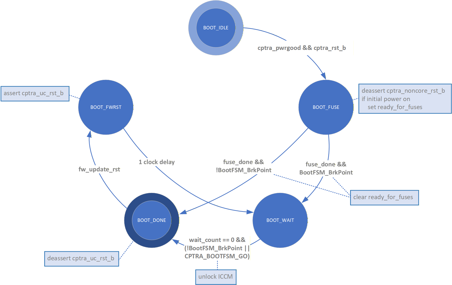
The Boot FSM first waits for the SoC to assert cptra_pwrgood and de-assert cptra_rst_b. In the BOOT_FUSE state, Caliptra signals to the SoC that it is ready for fuses. After the SoC is done writing fuses, it sets the fuse done register and the FSM advances to BOOT_DONE.
Once in the BOOT_DONE state, Caliptra de-asserts resets through a two flip-flop synchronizer.
FW update reset (Impactless FW update)
When a firmware update is initiated, Runtime FW writes to fw_update_reset register to trigger the FW update reset. When this register is written, only the RISC-V core is reset using cptra_uc_rst_b pin and all AHB targets are still active. All registers within the targets and ICCM/DCCM memories are intact after the reset. Reset is deasserted synchronously after a programmable number of cycles; the minimum allowed number of wait cycles is 5, which is also the default configured value. Reset de-assertion is done through a two flip-flop synchronizer. Since ICCM is locked during runtime, the boot FSM unlocks it when the RISC-V reset is asserted. Following FW update reset deassertion, normal boot flow updates the ICCM with the new FW from the mailbox SRAM.
Impactless firmware updates may be initiated by writing to the fw_update_reset register after Caliptra comes out of global reset and enters the BOOT_DONE state. In the BOOT_FWRST state, only the reset to the RISC-V core is asserted and the wait timer is initialized. After the timer expires, the FSM advances from the BOOT_WAIT to BOOT_DONE state where the reset is deasserted and ICCM is unlocked.
Breakpoints for Debug
Integrators may connect a breakpoint input to Caliptra, which is intended to connect to a chip GPIO pin. When asserted, this pin causes the Caliptra boot FSM to follow a modified arc. Instead of transitioning immediately to the BOOT_DONE state upon completion of fuse programming, the state machine transitions from BOOT_FUSE to BOOT_WAIT. Here, the state machine halts until the Caliptra register CPTRA_BOOTFSM_GO is set, either by AXI or TAP access.
RISC-V core
The RISC-V core is VeeR EL2 from CHIPS Alliance. It is a 32-bit CPU core that contains a 4-stage, scalar, in-order pipeline. The core supports RISC-V’s integer(I), compressed instruction(C), multiplication and division (M), instruction-fetch fence, CSR, and subset of bit manipulation instructions (Z) extensions. A link to the RISC-V VeeR EL2 Programmer’s Reference Manual is provided in the References section.
Configuration
The RISC-V core is highly configurable and has the following settings.
| Parameter | Configuration |
|---|---|
| Interface | AHB-Lite |
| DCCM | 256 KiB |
| ICCM | 256 KiB |
| I-Cache | Disabled |
| Reset Vector | 0x00000000 |
| Fast Interrupt Redirect | Enabled |
| External Interrupts | 31 |
| PMP | Enabled |
Embedded memory export
Internal RISC-V SRAM memory components are exported from the Caliptra subsystem to support adaptation to various fabrication processes. For more information, see the Caliptra Integration Specification.
Memory map address regions
The 32-bit address region is subdivided into 16 fixed-sized, contiguous 256 MB regions. The following table describes the address mapping for each of the AHB devices that the RISC-V core interfaces with.
| Subsystem | Address size | Start address | End address |
|---|---|---|---|
| ROM | 96 KiB | 0x0000_0000 | 0x0000_BFFF |
| Cryptographic | 512 KiB | 0x1000_0000 | 0x1007_FFFF |
| Peripherals | 32 KiB | 0x2000_0000 | 0x2000_7FFF |
| SoC IFC | 512 KiB | 0x3000_0000 | 0x3007_FFFF |
| RISC-V Core ICCM | 256 KiB | 0x4000_0000 | 0x4003_FFFF |
| RISC-V Core DCCM | 256 KiB | 0x5000_0000 | 0x5003_FFFF |
| RISC-V MM CSR (PIC) | 256 MiB | 0x6000_0000 | 0x6FFF_FFFF |
Cryptographic subsystem
The following table shows the memory map address ranges for each of the IP blocks in the cryptographic subsystem.
| IP/Peripheral | Target # | Address size | Start address | End address |
|---|---|---|---|---|
| Cryptographic Initialization Engine | 0 | 32 KiB | 0x1000_0000 | 0x1000_7FFF |
| ECC Secp384 | 1 | 32 KiB | 0x1000_8000 | 0x1000_FFFF |
| HMAC512 | 2 | 4 KiB | 0x1001_0000 | 0x1001_0FFF |
| Key Vault | 3 | 8 KiB | 0x1001_8000 | 0x1001_9FFF |
| PCR Vault | 4 | 8 KiB | 0x1001_A000 | 0x1001_BFFF |
| Data Vault | 5 | 8 KiB | 0x1001_C000 | 0x1001_DFFF |
| SHA512 | 6 | 32 KiB | 0x1002_0000 | 0x1002_7FFF |
| SHA256 | 10 | 32 KiB | 0x1002_8000 | 0x1002_FFFF |
| ABR (MLDSA/MLKEM) | 14 | 64 KiB | 0x1003_0000 | 0x1003_FFFF |
| AES | 15 | 4 KiB | 0x1001_1000 | 0x1001_1FFF |
| SHA3 | 16 | 4 KiB | 0x1004_0000 | 0x1004_0FFF |
Peripherals subsystem
The following table shows the memory map address ranges for each of the IP blocks in the peripherals’ subsystem.
| IP/Peripheral | Target # | Address size | Start address | End address |
|---|---|---|---|---|
| CSRNG | 12 | 4 KiB | 0x2000_2000 | 0x2000_2FFF |
| ENTROPY SRC | 13 | 4 KiB | 0x2000_3000 | 0x2000_3FFF |
SoC interface subsystem
The following table shows the memory map address ranges for each of the IP blocks in the SoC interface subsystem.
| IP/Peripheral | Target # | Address size | Start address | End address |
|---|---|---|---|---|
| Mailbox CSR | 7 | 4 KiB | 0x3002_0000 | 0x3002_0FFF |
| SHA512 Accelerator | 7 | 4 KiB | 0x3002_1000 | 0x3002_1FFF |
| AXI DMA | 7 | 4 KiB | 0x3002_2000 | 0x3002_2FFF |
| SOC IFC CSR | 7 | 64 KiB | 0x3003_0000 | 0x3003_FFFF |
| Mailbox SRAM Direct Access | 7 | 256 KiB | 0x3004_0000 | 0x3007_FFFF |
RISC-V core local memory blocks
The following table shows the memory map address ranges for each of the local memory blocks that interface with RISC-V core.
| IP/Peripheral | Target # | Address size | Start address | End address |
|---|---|---|---|---|
| ICCM0 (via DMA) | 9 | 256 KiB | 0x4000_0000 | 0x4003_FFFF |
| DCCM | 8 | 256 KiB | 0x5000_0000 | 0x5003_FFFF |
Interrupts
The VeeR-EL2 processor supports multiple types of interrupts, including non-maskable interrupts (NMI), software interrupts, timer interrupts, external interrupts, and local interrupts. Local interrupts are events not specified by the RISC-V standard, such as auxiliary timers and correctable errors.
Caliptra uses NMI in conjunction with a watchdog timer to support fatal error recovery and system restart. For more information, see the Watchdog timer section.
Software and local interrupts are not implemented in the first generation of Caliptra. Standard RISC-V timer interrupts are implemented using the mtime and mtimecmp registers defined in the RISC-V Privileged Architecture Specification. Both mtime and mtimecmp are included in the soc_ifc register bank, and are accessible by the internal microprocessor to facilitate precise timing tasks. Frequency for the timers is configured by the SoC using the dedicated timer configuration register, which satisfies the requirement prescribed in the RISC-V specification for such a mechanism. These timer registers drive the timer_int pin into the internal microprocessor.
Non-maskable interrupts
Caliptra's RISC-V processor has access to an internal register that allows configuration of the NMI vector. When an NMI occurs, the program counter jumps to the address indicated by the contents of this register. For more information, see NMI Vector.
External interrupts
Caliptra uses the external interrupt feature to support event notification from all attached peripheral components in the subsystem. The RISC-V processor supports multiple priority levels (ranging from 1-15), which allows firmware to configure interrupt priority per component.
Errors and notifications are allocated as interrupt events for each component, with error interrupts assigned a higher priority and expected to be infrequent.
Notification interrupts are used to alert the processor of normal operation activity, such as completion of requested operations or arrival of SoC requests through the shared interface.
Vector 0 is reserved by the RISC-V processor and may not be used, so vector assignment begins with Vector 1. Bit 0 of the interrupt port to the processor corresponds with Vector 1. The following table shows assignment of interrupt vectors to the corresponding IP block. The illustrated interrupt priority assignment is only an example, and does not correspond with actual priorities assigned in the final Caliptra firmware. These interrupt priorities are used in the validation firmware that tests the RTL, and are defined in caliptra_defines.h.
| IP/Peripheral | Interrupt vector | Interrupt priority example (Increasing, Max 15) |
|---|---|---|
| Cryptographic Initialization Engine (Errors) | 1 | 8 |
| Cryptographic Initialization Engine (Notifications) | 2 | 7 |
| ECC (Errors) | 3 | 8 |
| ECC (Notifications) | 4 | 7 |
| HMAC (Errors) | 5 | 8 |
| HMAC (Notifications) | 6 | 7 |
| Key Vault (Errors) | 7 | 8 |
| Key Vault (Notifications) | 8 | 7 |
| SHA512 (Errors) | 9 | 8 |
| SHA512 (Notifications) | 10 | 7 |
| SHA256 (Errors) | 11 | 8 |
| SHA256 (Notifications) | 12 | 7 |
| RESERVED | 13, 15, 17 | 4 |
| RESERVED | 14, 16, 18 | 3 |
| Mailbox (Errors) | 19 | 8 |
| Mailbox (Notifications) | 20 | 7 |
| SHA512 Accelerator (Errors) | 23 | 8 |
| SHA512 Accelerator (Notifications) | 24 | 7 |
| ABR (MLDSA/MLKEM) (Errors) | 23 | 8 |
| ABR (MLDSA/MLKEM) (Notifications) | 24 | 7 |
| AXI DMA (Errors) | 25 | 8 |
| AXI DMA (Notifications) | 26 | 7 |
Watchdog timer
The primary function of Caliptra Watchdog Timer (WDT) is to reset the microcontroller (Caliptra), in the event of a software malfunction, by resetting the device if it has not been cleared in software. It is a two-stage timer, independent of the RISCV core.
Operation
The WDT consists of two timers. When enabled in cascade mode (done by enabling Timer 1 alone), the WDT increments Timer 1 until the counter rolls over or times out. Typically, the timer is serviced at regular intervals to prevent it from overflowing or rolling over. If Timer 1 has not timed out, Timer 2 is disabled and held at its initial value. However, when Timer 1 does roll over, it triggers an error interrupt to the RISC-V core. In parallel, Timer 2 is enabled and begins counting. If the interrupt is serviced before Timer 2 times out, the timers are reset and continue to operate normally. If Timer 2 times out, it asserts an SoC fatal error and an NMI. The SoC fatal error is also captured in the CPTRA_HW_ERROR_FATAL register, which can be cleared by the SoC by writing a 1. A warm reset is required by the SoC to reset the timers when Timer 2 times out.
The WDT timers can be configured to operate independent of each other. When the enable register for Timer 2 is set, the default configuration of cascaded timers is disabled and both timers count independently of each other. In this case, a timeout on Timer 2 causes an error interrupt to the RISC-V core similar to Timer 1. Disabling Timer 2 configures the timers back into the default cascaded mode.
Each timer has an enable bit, a restart bit, and a 64-bit timeout value register that can be programmed as needed. The restart bit is used to service the timers and restart counting. The timeout period registers can be configured to the desired upper bound of timers.
If the WDT timers are disabled and then re-enabled with a new timeout period, they must be restarted by setting the appropriate control register (restart bit). If the timers are temporarily disabled and re-enabled with the same timeout period, they resume counting and do not restart from 0.
For more details regarding the register interface to control the WDT, see the register documentation published in the RTL GitHub repository.
The following figure shows the two timers.
Figure: Caliptra Watchdog Timer
Prescale settings
Assuming a clock source of 500 MHz, a timeout value of 32’hFFFF_FFFF results in a timeout period of ~8.5 seconds. Two 32-bit registers are provided for each timer, allowing a 64-bit timeout period to be programmed for each timer. This accommodates a maximum timeout value of over 1000 years for the same 500 Mhz clock source.
Microcontroller interface
The Caliptra microcontroller communicates with the mailbox through its internal AHB-Lite fabric.
AHB-lite interface
AHB-lite is a subset of the full AHB specification. It is primarily used in single initiator systems. This interface connects VeeR EL2 Core (LSU initiator) to the target devices. See Caliptra Core for information.
The interface can be customized to support variable address and data widths, and a variable number of target devices. Each target device is assigned an address range within the 32-bit address memory map region. The interface includes address decoding logic to route data to the appropriate AHB target device based on the address specified.
The integration parameters for Caliptra’s AHB-lite interface are shown in the following table.
| Parameter | Value |
|---|---|
| ADDRESS_WIDTH | 32 |
| DATA_WIDTH | 64 |
| NUM_OF_SLAVES | 17 |
Each IP component in the Caliptra system uses a native AHB data width of 32-bits (1 dword). The AHB responder logic in each IP component contains width conversion logic that transforms from the fabric data width of 64-bits to this native 32-bit width. The conversion involves calculating the dword offset (either 0 or 1) relative to the native 64-bit width by evaluating bit [2] of the address line. This information is used to extract the correct 32-bits from the native write data line. If there is a data offset, data is shifted down by 32-bits; otherwise, the upper 32-bits are simply truncated. This new dword-address is passed to the internal register interface along with the dword-sized data. A similar conversion works in reverse to correctly place read data in the response data line from the responder.
As a result of this implementation, 64-bit data transfers are not supported on the Caliptra AHB fabric. Firmware running on the internal microprocessor may only access memory and registers using a 32-bit or smaller request size, as 64-bit transfer requests will be corrupted.
All AHB requests internal to Caliptra must be to an address that is aligned to the native data width of 4-bytes. Any AHB read or write by the Caliptra RISC-V processor that is not aligned to this boundary will fail to decode to the targeted register, will fail to write the submitted data, and will return read data of all zeroes. All AHB requests must also use the native size of 4 bytes (encoded in the hsize signal with a value of 2). The only exception to this is when the RISC-V processor performs byte-aligned, single-byte reads to the Mailbox SRAM using the direct-access mechanism described in SoC Mailbox. In this case, a byte-aligned address must be accompanied by the correct size indicator for a single-byte access. Read addresses for byte accesses are aligned to the 4-byte boundary in hardware, and will successfully complete with the correct data at the specified byte offset. Direct mode SRAM writes must be 4-bytes in size and must be aligned to the 4-byte boundary. Hardware writes the entire dword of data to the aligned address, so attempts to write a partial word of data may result in data corruption.
Cryptographic subsystem
For details, see the Cryptographic subsystem architecture section.
SoC mailbox
For more information on the mailbox protocol, see Mailbox in the Caliptra Integration Specification. Mailbox registers accessible to the Caliptra microcontroller are defined in internal-regs/mbox_csr.
The RISC-V processor is able to access the SoC mailbox SRAM using a direct access mode (which bypasses the defined mailbox protocol). The addresses for performing this access are described in SoC interface subsystem and in mbox_sram. In this mode, firmware must first acquire the mailbox lock. Then, reads and writes to the direct access address region will go directly to the SRAM block. Firmware must release the mailbox lock by writing to the mbox_unlock register after direct access operations are completed.
Security state
Caliptra uses the MSB of the security state input to determine whether or not Caliptra is in debug mode.
When Caliptra is in debug mode:
-
Security state MSB is set to 0.
-
Caliptra JTAG is opened for the microcontroller and HW debug.
-
Device secrets (UDS, FE, key vault, csr hmac key and obfuscation key) are programmed to debug values.
If a transition to debug mode happens during ROM operation, any values computed from the use of device secrets may not match expected values.
Transitions to debug mode trigger a hardware clear of all device secrets, and also trigger an interrupt to FW to inform of the transition. FW is responsible for initiating another hardware clear of device secrets utilizing the clear secrets register, in case any derivations were in progress and stored after the transition was detected. FW may open the JTAG after all secrets are cleared.
Debug mode values may be set by integrators in the Caliptra configuration files. The default values are shown in the following table.
| Name | Default value |
|---|---|
| Obfuscation Key Debug Value | All 0x1 |
| CSR HMAC Key Debug Value | All 0x1 |
| UDS Debug Value | All 0x1 |
| Field Entropy Debug Value | All 0x1 |
| Key Vault Debug Value 0 | All 0xA |
| Key Vault Debug Value 1 | All 0x5 |
Note: When entering debug or scan mode, all crypto engines are zeroized. Before starting any crypto operation in these modes, the status registers of all crypto engines must be checked to confirm they are ready. Failing to do so may trigger a fatal error caused by concurrent crypto operations.
Clock gating
Caliptra provides a clock gating feature that turns off clocks when the microcontroller is halted. Clock gating is disabled by default, but can be globally enabled via the following register.
| Control register | Start address | Description |
|---|---|---|
| CPTRA_CLK_GATING_EN | 0x300300bc | Register bit to enable or disable the clock gating feature. |
When enabled, halting the microcontroller turns off clocks to all of the cryptographic subsystem, the vaults (key vault, PCR vault, and data vault), mailbox SRAM, SoC interface, and peripherals subsystem. The Watchdog timer and SoC registers run on the gated RDC clock. The RV core implements its own clock gating mechanism. Halting the core automatically turns off its clock.
There are a total of 4 clocks in Caliptra: ungated clock, gated clock, gated RDC clock, and gated SoC IFC clock. The following table shows the different modules and their designated clocks.
| Module | Clock |
|---|---|
| RV core | Clk |
| SOC IFC | Clk; clk_cg; rdc_clk_cg; soc_ifc_clk_cg |
| Crypto subsystem | Clk_cg |
| Vaults | Clk_cg |
| Peripherals subsystem | Clk_cg |
| AHB Lite IF, 2to1 Mux | Clk_cg |
| TRNG | Clk_cg |
Wake up conditions
For details on halting the core and waking up the core from the halt state, see section 5 of the RISC-V VeeR EL2 Programmer's Reference Manual.
When the RV core wakes up, all clocks are enabled. However, when the core is halted, it is possible to wake up Caliptra clocks through:
-
A change in generic_input_wires
-
Cptra_fatal_error assertion
-
Entry to debug or scan modes
-
JTAG accesses
-
AXI transactions
Activity on the AXI subordinate interface only wakes up the SoC IFC clock. All other clocks remain off until any other condition is met or the core exits the halt state.
| Cpu_halt_status | s_axi_active | Generic input wires || fatal error || debug/scan mode ||JTAG access | Expected behavior |
|---|---|---|---|
| 0 | X | X | All gated clocks active |
| 1 | 0 | 0 | All gated clocks inactive |
| 1 | 0 | 1 | All gated clocks active (as long as condition is true) |
| 1 | 1 | 0 | Soc_ifc_clk_cg active (as long as s_axi_active = 1) All other clks inactive |
| 1 | 1 | 1 | Soc_ifc_clk_cg active (as long as condition is true OR s_axi_active = 1) All other clks active (as long as condition is true) |
Usage
The following applies to the clock gating feature:
- The core should only be halted after all pending vault writes are done and cryptographic operations are complete.
- While the core is halted, any AXI transaction wakes up the SoC interface clock and leaves all other clocks disabled. If the core is still halted when the AXI transactions are done, the SoC interface clock is returned to a disabled state. .
- The RDC clock is similar to an ungated clock and is only disabled when a reset event occurs. This avoids metastability on flops. The RDC clock operates independently of core halt status.
Timing information
The following figure shows the timing information for clock gating.
Figure: Clock gating timing
Integrated TRNG
Caliptra implements a true random number generator (TRNG) block for local use models. Firmware is able to read a random number from the TRNG core by accessing its register block over the AHB-lite interface. This is a configuration that SoC integrators enable by defining CALIPTRA_INTERNAL_TRNG.
This TRNG block is a combination of entropy source and CSRNG implementations. For information, see the ENTROPY_SRC HWIP Technical Specification and the CSRNG HWIP Technical Specification. The core code (see entropy source and csrng) is reused from here but the interface to the module is changed to AHB-lite. This design provides an interface to an external physical random noise generator. This is also referred to as a physical true random number generator (PTRNG). The PTRNG external source is a physical true random noise source. A noise source and its relation to an entropy source are defined by SP 800-90B.
The block is instantiated based on a design parameter chosen at integration time. This is to provide options for SoC to reuse an existing TRNG to build an optimized SoC design. For the optimized scenarios, SoC needs to follow the External-TRNG REQ HW API.
The following figure shows the integrated TRNG block.
Figure: Integrated TRNG block
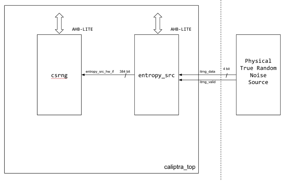
The following figure shows the CSRNG block.
Figure: CSRNG block
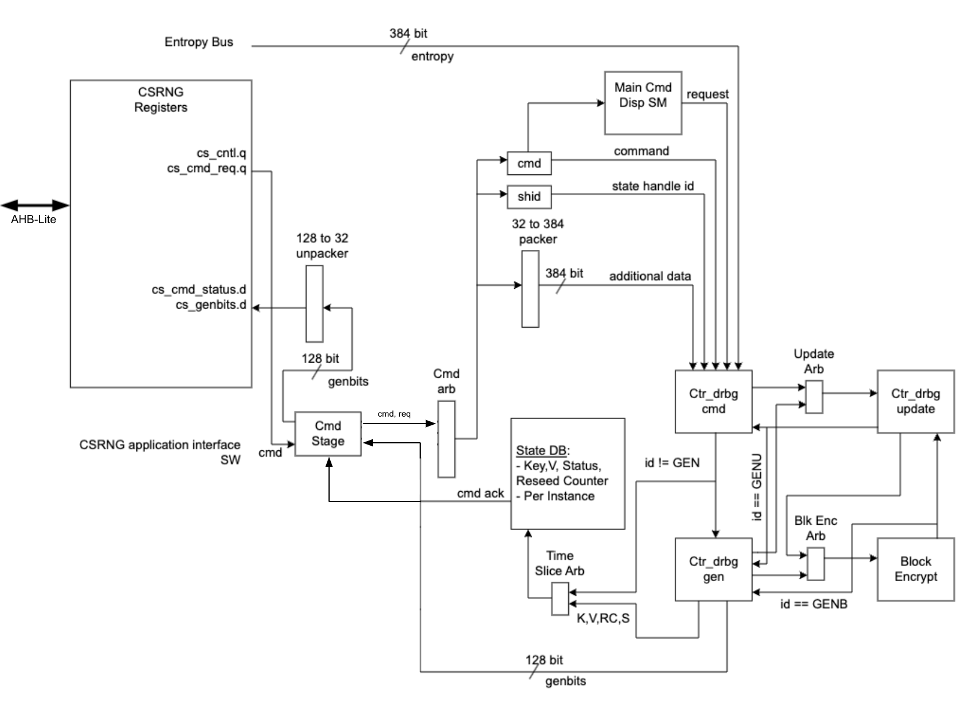
The following figure shows the entropy source block.
Figure: Entropy source block
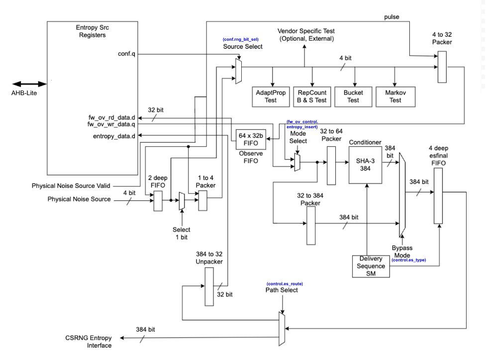
Operation
Requests for entropy bits start with command requests over the AHB-lite interface to the csrng CMD_REQ register.
The following describes the fields of the command request header:
-
Application Command: Selects one of five operations to perform. The commands supported are instantiate, reseed, generate, update, and uninstantiate.
-
Command Length: Number of 32-bit words that can optionally be appended to the command. A value of zero will only transfer the command header. A value of 4'hc transfers the header plus an additional twelve 32-bit words of data.
-
Command Flag0: flag0 is associated with the current command. Setting this field to True (4’h6) enables flag0 to be enabled. Note that flag0 is used for the instantiate and reseed commands only; for all other commands, the flag0 value is ignored.
-
Generate Length: Only defined for the generate command, this field is the total number of cryptographic entropy blocks requested. Each unit represents 128 bits of entropy returned. A value of 8 would return a total of 1024 bits. The maximum size supported is 4096.
First an instantiate command is requested over the SW application interface to initialize an instance in the CSRNG module. Depending on the flag0 and clen fields in the command header, a request to the entropy_src module over the entropy interface is sent to seed the csrng. This can take a few milliseconds if the seed entropy is not immediately available.
Example instantiation:
acmd = 0x1 (Instantiate)
clen/flag0 = The seed behavior is described in the following table.
glen = Not used
| flag0 | clen | Description |
|---|---|---|
| F | 0 | Only entropy source seed is used. |
| F | 1-12 | Entropy source seed is xor'ed with provided additional data. |
| T | 0 | Seed of zero is used (no entropy source seed used). |
| T | 1-12 | Only provided additional data is used as seed. |
Next a generate command is used to request generation of cryptographic entropy bits. The glen field defines how many 128 bit words are to be returned to the application interface. After the generated bits are ready, they can be read out via the GENBITS register. This register must be read out glen * 4 times for each request made.
Example generate command:
acmd = 0x3 (Generate)
clen = 0
flag0 = false (4’h9)
glen = 4 (4 *128 = 512b)
This requires 16 reads from GENBITS to read out all of the generated entropy.
Configuration
The HW application interfaces are not supported. Only the SW application interface should be used for this design.
Physical true random noise source signal descriptions
These are the top level signals defined in caliptra_top.
| Name | Input or output | Description |
|---|---|---|
| itrng_data | input | Physical true random noise source data |
| itrng_valid | input | Valid is asserted high for one cycle when data is valid. The expected valid output rate is about 50KHz. |
The following figure shows the top level signals defined in caliptra_top.
Figure: caliptra_top signals
Entropy source signal descriptions
The following table provides descriptions of the entropy source signals.
| Name | Input or output | Description |
|---|---|---|
| clk_i | input | All signal timings are related to the rising edge of clk. |
| rst_ni | input | The reset signal is active LOW and resets the core. |
| entropy_src_rng_req | output | Request from the entropy_src module to the physical true random noise source to start generating data. |
| entropy_src_rng_rsp | input | Contains the internal TRNG data and a flag indicating the data is valid. Valid is asserted high for one cycle when data is valid. |
| entropy_src_hw_if_i | input | Downstream block request for entropy bits. |
| entropy_src_hw_if_o | output | 384 bits of entropy data. Valid when es_ack is asserted high. |
| cs_aes_halt_i | input | Response from csrng that all requests to AES block are halted. |
| cs_aes_halt_o | output | Request to csrng to halt requests to the AES block for power leveling purposes. |
The following figure shows the entropy source signals.
Figure: Entropy source signals
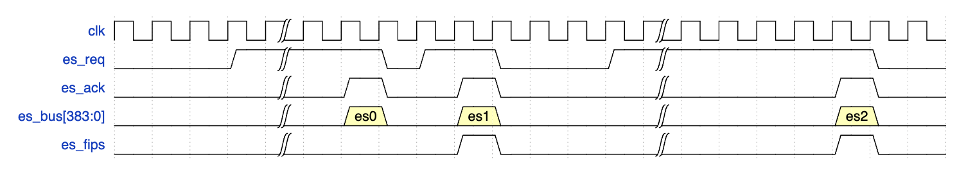
CSRNG signal descriptions
The following table provides descriptions for the CSRNG signals.
| Name | Input or output | Description |
|---|---|---|
| clk_i | input | All signal timings are related to the rising edge of clk. |
| rst_ni | input | The reset signal is active LOW and resets the core. |
| otp_en_csrng_sw_app_read_i | input | Enable firmware to access the ctr_drbg internal state and genbits through registers. |
| lc_hw_debug_en_i | input | Lifecycle that selects which diversification value is used for xoring with the seed from entropy_src. |
| entropy_src_hw_if_i | input | 384 bits of entropy data. Valid when es_ack is asserted high. |
| entropy_src_hw_if_o | output | Downstream block request for entropy bits. |
| cs_aes_halt_i | input | Request from entropy_src to halt requests to the AES block for power leveling purposes. |
| cs_aes_halt_o | output | Response to entropy_src that all requests to AES block are halted. |
The CSRNG may only be enabled if entropy_src is enabled. After it is disabled, CSRNG may only be re-enabled after entropy_src has been disabled and re-enabled.
FIPS considerations
The following sections illustrate the self-test parameter configuration. The
entropy_src block provides additional tests, but Caliptra focuses primarily
on the adaptive and repetition count tests, which are the ones strictly
required for FIPS compliance. Additional details can be found in NIST
publication SP 800-90B.
The TRNG must be re-initialized whenever self-test parameter changes are needed. As described in the previous section, the initialization steps are as follows:
- Disable
csrngandentropy_srcin that order. - Apply new self-test configuration.
- Enable
entropy_srcandcsrngin that order.
Adaptive self-test window and thresholds
This section details the configuration of the entropy_src, focusing on how
the test window size for the adaptive self-test is determined and how it
relates to threshold calculations.
Understanding Test Window Sizes
The adaptive self-test within the entropy_src block utilizes a
configurable test window. To clarify its interpretation, two terms are
defined:
ENTROPY_TEST_WINDOW: This refers to the test window size directly configured in the hardware registers of theentropy_srcblock.ACTUAL_TEST_WINDOW: This refers to the effective window size used for the adaptive self-test threshold calculations. Its value depends on how the test scores are aggregated.
The aggregation method is determined by the CONF.THRESHOLD_SCOPE setting in the entropy_src block.
Aggregate per symbol
When CONF.THRESHOLD_SCOPE is enabled:
- The adaptive test combines the inputs from all physical entropy lines into a single, cumulative score.
- The test essentially treats the combined input as a single binary stream, counting the occurrences of '1's.
- In this configuration:
- If
ENTROPY_TEST_WINDOWis set to 1024, then ACTUAL_TEST_WINDOW=ENTROPY_TEST_WINDOW= 1024
- If
Handle each physical noise source separately
When CONF.THRESHOLD_SCOPE is disabled:
- The adaptive test scores each individual physical noise input line independently.
- This allows for monitoring the health of each noise source.
- In this configuration (assuming, for example, 4 noise sources):
- If
ENTROPY_TEST_WINDOWis set to 4096 bits, then ACTUAL_TEST_WINDOW= (ENTROPY_TEST_WINDOW/ 4) = 1024
- If
Configuring adaptive self-test thresholds
Once the ACTUAL_TEST_WINDOW is determined, the adaptive self-test
thresholds can be configured as follows:
ADAPTP_HI_THRESHOLDS.FIPS_THRESH=adaptp_cutoffADAPTP_LO_THRESHOLDS.FIPS_THRESH=ACTUAL_TEST_WINDOW-adaptp_cutoff
Here, adaptp_cutoff represents the pre-determined cutoff value for the
adaptive proportion test, as defined by NIST SP 800-90B. See the threshold
calculations below as an example.
\(α = 2^{-40}\) (recommended)
\(H = 0.5\) (example, estimated entropy measured from hardware)
\(W\) = ACTUAL_TEST_WINDOW
adaptp_cutoff = \(1 + critbinom(W, 2^{-H}, 1 - α)\)
Note: The
critbinomfunction (critical binomial distribution function) is implemented by most spreadsheet applications.
Recommended configuration
The following configuration is recommended for the adaptive and repetition count tests:
Adaptive test
- Set
CONF.THRESHOLD_SCOPEto disabled. This allows the test to monitor and score each physical noise source individually, providing more granular health information. - Set
HEALTH_TEST_WINDOWS.FIPS_WINDOWto 4096 bits. This value serves as theENTROPY_TEST_WINDOW. With the current 4 noise source configuration, this is equivalent to 1024 bits per noise source, where each source produces 1 bit of entropy as defined in NIST SP 800-90B. - Calculate thresholds. Use an
ACTUAL_TEST_WINDOWof 1024 bits (derived from step 2) in the adaptive test threshold formulas provided earlier in this subsection.
Repetition count test
The methodology used for calculating the repetition count threshold in the ROM boot phase can be directly applied for this test as well. The threshold is applied on a per-noise-source basis.
External-TRNG REQ HW API
For SoCs that choose to not instantiate Caliptra’s integrated TRNG, Caliptra provides a TRNGREQ HW API.
- Caliptra asserts TRNG_REQ wire (FW made the request for a TRNG).
- SoC writes the TRNG architectural registers.
- SoC writes a done bit in the TRNG architectural registers.
- Caliptra desserts TRNG_REQ.
The reason to have a separate interface from the SoC mailbox is to ensure that this request is not intercepted by any SoC FW agents that communicate with the SoC mailbox. It is required for FIPS compliance that this TRNG HW API is always handled by a SoC HW gasket logic and not handled by SoC ROM/FW code.
SoC-SHA accelerator HW API
Caliptra provides a SHA accelerator HW API for Caliptra internal FW to use via mailbox or via DMA operations through the AXI subordinate interface. The SHA accelerator HW API is restricted on AXI for use by Caliptra via the AXI DMA assist block; this access restriction is enforced by checking logic on the AXI AxUSER signal associated with the request.
Using the HW API:
- A user of the HW API first locks the accelerator by reading the LOCK register. A read that returns the value 0 indicates that the resource was locked for exclusive use by the requesting user. A write of ‘1 clears the lock.
- The USER register captures the AXI USERID value of the requestor that locked the SHA accelerator. This is the only user that is allowed to control the SHA accelerator by performing AXI register writes. Writes by any other agent on the AXI subordinate interface are dropped.
- SHA supports Mailbox mode: SHA is computed on LENGTH (DLEN) bytes of data stored in the mailbox beginning at START_ADDRESS. This computation is performed when the EXECUTE register is set by the user. When the operation is completed and the result in the DIGEST register is valid, SHA accelerator sets the VALID bit of the STATUS register.
- Note that even though the mailbox size is fixed, due to SHA save/restore function enhancement, there is no limit on the size of the block that needs to be SHAd. SOC needs to follow FW API
- The SHA computation engine in the SHA accelerator requires big endian data, but the SHA accelerator can accommodate mailbox input data in either the little endian or big endian format. By default, input data is assumed to be little endian and is swizzled to big endian at the byte level prior to computation. For the big endian format, data is loaded into the SHA engine as-is. Users may configure the SHA accelerator to treat data as big endian by setting the ENDIAN_TOGGLE bit appropriately.
- See the register definition for the encodings.
- SHA engine also provides a ‘zeroize’ function through its CONTROL register to clear any of the SHA internal state. This can be used when the user wants to conceal previous state for debug or security reasons.
JTAG implementation
For specific debug flows, see the JTAG/TAP Debug section in Caliptra: A Datacenter System on a Chip (SoC) Root of Trust (RoT).
The following figure shows the JTAG implementation within the Caliptra boundary. The output of the existing DMI wrapper is used to find the non-Core (Caliptra uncore) aperture to route the JTAG commands.
Caliptra’s JTAG/TAP should be implemented as a TAP EP. JTAG is open if the debug mode is set at the time of Caliptra reset deassertion.
Note: If the debug security state switches to debug mode anytime, the security assets and keys are still flushed even though JTAG is not open.
The following table details the alias addresses for registers in soc ifc that are accessible through JTAG. Debug Locked registers are a subset of registers accessible when debug intent is set, when debug is unlocked, or the lifecycle state is DEVICE_MANUFACTURING. Debug Unlocked registers are accessible when debug is unlocked, or the lifecycle state is DEVICE_MANUFACTURING.
| Register Name | JTAG Address | Accessibility | Debug Locked | Debug Unlocked |
|---|---|---|---|---|
| mbox_lock | 7’h75 | RO | YES | YES |
| mbox_cmd | 7’h76 | RW | YES | YES |
| mbox_dlen | 7’h50 | RW | YES | YES |
| mbox_dataout | 7’h51 | RO | YES | YES |
| mbox_datain | 7’h62 | WO | YES | YES |
| mbox_status | 7’h52 | RW | YES | YES |
| mbox_execute | 7’h77 | WO | YES | YES |
| CPTRA_BOOT_STATUS | 7’h53 | RO | YES | YES |
| CPTRA_HW_ERRROR_ENC | 7’h54 | RO | YES | YES |
| CPTRA_FW_ERROR_ENC | 7’h55 | RO | YES | YES |
| SS_UDS_SEED_BASE_ADDR_L | 7’h56 | RO | YES | |
| SS_UDS_SEED_BASE_ADDR_H | 7’h57 | RO | YES | |
| CPTRA_HW_ERROR_FATAL | 7’h58 | RO | YES | YES |
| CPTRA_FW_ERROR_FATAL | 7’h59 | RO | YES | YES |
| CPTRA_HW_ERROR_NON_FATAL | 7’h5a | RO | YES | YES |
| CPTRA_FW_ERROR_NON_FATAL | 7’h5b | RO | YES | YES |
| CPTRA_DBG_MANUF_SERVICE_REG | 7’h60 | RW | YES | YES |
| CPTRA_BOOTFSM_GO | 7’h61 | RW | YES | YES |
| SS_DEBUG_INTENT | 7’h63 | RW | YES | |
| SS_CALIPTRA_BASE_ADDR_L | 7’h64 | RW | YES | |
| SS_CALIPTRA_BASE_ADDR_H | 7’h65 | RW | YES | |
| SS_MCI_BASE_ADDR_L | 7’h66 | RW | YES | |
| SS_MCI_BASE_ADDR_H | 7’h67 | RW | YES | |
| SS_RECOVERY_IFC_BASE_ADDR_L | 7’h68 | RW | YES | |
| SS_RECOVERY_IFC_BASE_ADDR_H | 7’h69 | RW | YES | |
| SS_OTP_FC_BASE_ADDR_L | 7’h6A | RW | YES | |
| SS_OTP_FC_BASE_ADDR_H | 7’h6B | RW | YES | |
| SS_STRAP_GENERIC_0 | 7’h6C | RW | YES | |
| SS_STRAP_GENERIC_1 | 7’h6D | RW | YES | |
| SS_STRAP_GENERIC_2 | 7’h6E | RW | YES | |
| SS_STRAP_GENERIC_3 | 7’h6F | RW | YES | |
| SS_DBG_SERVICE_REG_REQ | 7’h70 | RW | YES | YES |
| SS_DBG_SERVICE_REG_RSP | 7’h71 | RO | YES | YES |
| SS_DBG_UNLOCK_LEVEL0 | 7’h72 | RW | YES | |
| SS_DBG_UNLOCK_LEVEL1 | 7’h73 | RW | YES | |
| SS_STRAP_CALIPTRA_DMA_AXI_USER | 7’h74 | RW | YES | |
| SS_EXTERNAL_STAGING_AREA_BASE_ADDR_L | 7’h78 | RW | YES | |
| SS_EXTERNAL_STAGING_AREA_BASE_ADDR_H | 7’h79 | RW | YES |
Figure: JTAG implementation
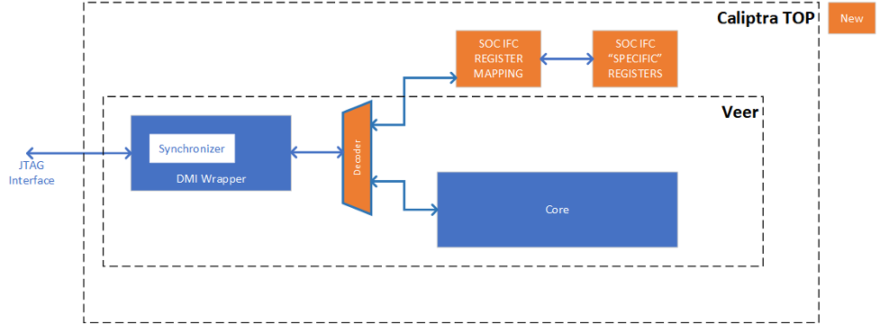
Cryptographic subsystem architecture
The architecture of Caliptra cryptographic subsystem includes the following components:
- Symmetric cryptographic primitives
- De-obfuscation engine
- SHA512/384 (based on NIST FIPS 180-4 [2])
- SHA256 (based on NIST FIPS 180-4 [2])
- HMAC512 (based on NIST FIPS 198-1 [5] and RFC 4868 [6])
- SHA3 (based on NIST FIPS 202 [17])
- Public-key cryptography
- NIST Secp384r1 Deterministic Digital Signature Algorithm (based on FIPS-186-4 [11] and RFC 6979 [7])
- Key vault
- Key slots
- Key slot management
The high-level architecture of Caliptra cryptographic subsystem is shown in the following figure.
Figure: Caliptra cryptographic subsystem

SHA512/SHA384
SHA512 is a function of cryptographic hash algorithm SHA-2. The hardware implementation is based on Secworks/SHA512 [1]. This implementation complies with the functionality in NIST FIPS 180-4 [2]. The implementation supports the SHA512 variants SHA-512/224, SHA-512/256, SHA384 and SHA512.
The SHA512 algorithm is described as follows:
- The message is padded by the host and broken into 1024-bit chunks
- For each chunk:
- The message is fed to the SHA512 core
- The core should be triggered by the host
- The SHA512 core status is changed to ready after hash processing
- The result digest can be read after feeding all message chunks
Operation
Padding
The message should be padded before feeding to the hash core. The input message is taken, and some padding bits are appended to it to get it to the desired length. The bits that are used for padding are simply ‘0’ bits with a leading ‘1’ (100000…000). The appended length of the message (before pre-processing), in bits, is a 128-bit big-endian integer.
The total size should be equal to 128 bits short of a multiple of 1024 since the goal is to have the formatted message size as a multiple of 1024 bits (N x 1024). The following figure shows the SHA512 input formatting.
Figure: SHA512 input formatting

Hashing
The SHA512 core performs 80 iterative operations to process the hash value of the given message. The algorithm processes each block of 1024 bits from the message using the result from the previous block. For the first block, the initial vectors (IV) are used for starting the chain processing of each 1024-bit block.
FSM
The SHA512 architecture has the finite-state machine as shown in the following figure.
Figure: SHA512 FSM
Signal descriptions
The SHA512 architecture inputs and outputs are described in the following table.
| Name | Inputs and outputs | Description |
|---|---|---|
| clk | input | All signal timings are related to the rising edge of clk. |
| reset_n | input | The reset signal is active LOW and resets the core. This is the only active LOW signal. |
| init | input | The core is initialized and processes the first block of message. |
| next | input | The core processes the rest of the message blocks using the result from the previous blocks. |
| mode[1:0] | input | Indicates the hash type of the function. This can be: - SHA512/224 - SHA512/256 - SHA384 - SHA512 |
| zeroize | input | The core clears all internal registers to avoid any SCA information leakage. |
| block[1023:0] | input | The input padded block of message. |
| ready | output | When HIGH, the signal indicates the core is ready. |
| digest[511:0] | output | The hashed value of the given block. |
| digest_valid | output | When HIGH, the signal indicates that the result is ready. |
Address map
The SHA512 address map is shown here: sha512_reg -- clp Reference (chipsalliance.github.io)
Pseudocode
The following pseudocode demonstrates how the SHA512 interface can be implemented.
Figure: SHA512 pseudocode
SCA countermeasure
We do not propose any countermeasure to protect the hash functions. Inherently, hash functions do not work like other cryptographic engines. Hash functions target integrity without requiring a secret key. Hence, the attacker can target only messages. Also, the attacker cannot build a CPA or DPA platform on the hash function because the same message ideally gives the same side-channel behavior.
If the attacker works on the multi-message mechanism, the attacker then needs to work with single trace attacks, which are very unlikely in ASIC/FPGA implementations. Also, our hash implementation is a noisy platform. As a result, we do not propose any SCA implementation countermeasure on the hash functions.
Performance
The SHA512 core performance is reported considering two different architectures: pure hardware architecture, and hardware/software architecture. These are described next.
Pure hardware architecture
In this architecture, the SHA512 interface and controller are implemented in hardware. The performance specification of the SHA512 architecture is shown in the following table.
| Operation | Cycle count [CCs] | Time [us] @ 400 MHz | Throughput [op/s] |
|---|---|---|---|
| Data_In transmission | 0.08 | ||
| Process | 87 | 0.22 | |
| Data_Out transmission | 16 | 0.04 | |
| Single block | 136 | 0.34 | 2,941,176 |
| Double block | 224 | 0.56 | 1,785,714 |
| 1 KiB message | 840 | 2.10 | 476,190 |
| 128 KiB message | 17,632 | 44.08 | 22,686 |
Hardware/software architecture
In this architecture, the SHA512 interface and controller are implemented in RISC-V core. The performance specification of the SHA512 architecture is shown in the following table.
| Operation | Cycle count [CCs] | Time [us]] @ 400 MHz | Throughput [op/s] |
|---|---|---|---|
| Data_In transmission | 990 | 2.48 | |
| Process | 139 | 0.35 | |
| Data_Out transmission | 387 | 0.97 | |
| Single block | 1,516 | 3.79 | 263,852 |
| Double block | 2,506 | 6.27 | 159,617 |
| 1 KiB message | 9,436 | 23.59 | 42,391 |
| 128 KiB message | 1,015,276 | 2,538.19 | 394 |
Pure software architecture
In this architecture, the SHA512 algorithm is implemented fully in software. The implementation is derived from the OpenSSL SHA512 implementation [3]. The performance numbers for this architecture are shown in the following table.
| Data size | Cycle count |
|---|---|
| 1 KiB | 147,002 |
| 4 KiB | 532,615 |
| 8 KiB | 1,046,727 |
| 12 KiB | 1,560,839 |
| 128 KiB | 16,470,055 |
SHA256
SHA256 is a function of the SHA-2 cryptographic hash algorithm. The hardware implementation is based on Secworks/SHA256 [1]. The implementation supports the two variants: SHA256/224 and SHA256.
The SHA256 algorithm is described as follows:
- The message is padded by the host and broken into 512-bit chunks
- For each chunk:
- The message is fed to the sha256 core
- The core should be triggered by the host
- The sha256 core status is changed to ready after hash processing
- The result digest can be read after feeding all message chunks
Operation
Padding
The message should be padded before feeding to the hash core. The input message is taken, and some padding bits are appended to the message to get it to the desired length. The bits that are used for padding are simply ‘0’ bits with a leading ‘1’ (100000…000). The appended length of the message (before pre-processing), in bits, is a 64-bit big-endian integer.
The total size should be equal to 64 bits, short of a multiple of 512 because the goal is to have the formatted message size as a multiple of 512 bits (N x 512).
The following figure shows SHA256 input formatting.
Figure: SHA256 input formatting
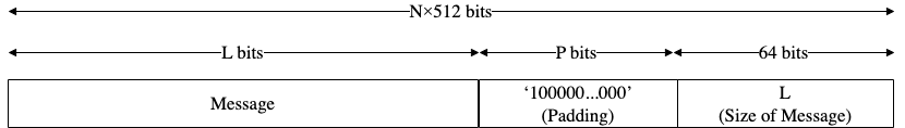
Hashing
The SHA256 core performs 64 iterative operations to process the hash value of the given message. The algorithm processes each block of 512 bits from the message using the result from the previous block. For the first block, the initial vectors (IV) are used to start the chain processing of each 512-bit block.
FSM
The SHA256 architecture has the finite-state machine as shown in the following figure.
Figure: SHA256 FSM
Signal descriptions
The SHA256 architecture inputs and outputs are described as follows.
| Name | Input or output | Description |
|---|---|---|
| clk | input | All signal timings are related to the rising edge of clk. |
| reset_n | input | The reset signal is active LOW and resets the core. This is the only active LOW signal. |
| init | input | The core is initialized and processes the first block of message. |
| next | input | The core processes the rest of the message blocks using the result from the previous blocks. |
| mode | input | Indicates the hash type of the function. This can be: - SHA256/224 - SHA256 |
| zeroize | input | The core clears all internal registers to avoid any SCA information leakage. |
| WNTZ_MODE* | input | SHA256 core is configured in Winternitz verification mode. |
| WNTZ_W[3:0]* | input | Winternitz W value. |
| WNTZ_N_MODE* | input | Winternitz n value(SHA192/SHA256 --> n = 24/32) |
| block[511:0] | input | The input padded block of message. |
| ready | output | When HIGH, the signal indicates the core is ready. |
| digest[255:0] | output | The hashed value of the given block. |
| digest_valid | output | When HIGH, the signal indicates the result is ready. |
* For more imformation about these inputs, please refer to LMS accelerator section.
Address map
The SHA256 address map is shown here: sha256_reg -- clp Reference (chipsalliance.github.io).
Pseudocode
The following pseudocode demonstrates how the SHA256 interface can be implemented.
Figure: SHA256 pseudocode
SCA countermeasure
We do not propose any countermeasure to protect the hash functions. For more information, see SCA countermeasure in the SHA512/SHA384 section.
Performance
The SHA256 core performance is reported considering two different architectures: pure hardware architecture, and hardware/software architecture. These are described next.
Pure hardware architecture
In this architecture, the SHA256 interface and controller are implemented in hardware. The performance specification of the SHA256 architecture is reported as shown in the following table.
| Operation | Cycle count [CCs] | Time [us] @ 400 MHz | Throughput [op/s] |
|---|---|---|---|
| Data_In transmission | 17 | 0.04 | |
| Process | 66 | 0.17 | |
| Data_Out transmission | 8 | 0.02 | |
| Single block | 91 | 0.23 | 4,395,604 |
| Double block | 158 | 0.40 | 2,531,646 |
| 1 KiB message | 1163 | 2.91 | 343,938 |
Hardware/software architecture
In this architecture, the SHA256 interface and controller are implemented in RISC-V core. The performance specification of the SHA256 architecture is reported as shown in the following table.
| Operation | Cycle count [CCs] | Time [us] @ 400 MHz | Throughput [op/s] |
|---|---|---|---|
| Data_In transmission | 500 | 1.25 | |
| Process | 66 | 0.17 | |
| Data_Out transmission | 195 | 0.49 | |
| Single block | 761 | 1.90 | 525,624 |
| Double block | 1355 | 3.39 | 295,203 |
| 1 KiB message | 8761 | 21.90 | 45,657 |
SHA3
The SHA3 HWIP performs the hash functions, whose purpose is to check the integrity of the received message. It supports various SHA3 hashing functions including SHA3 Extended Output Function (XOF) known as SHAKE functions. The details of the operation are described in the SHA3 specification, FIPS 202 known as sponge construction. It has been adapted from OpenTitan and you can find documentation describing the functionality of the KMAC block it was derived from here. In the current use cases of the SHA3 HW IP, either (a) messages are not considered secret (External Mu), or (b) SCA hardening would not be meaningful (HPKE in OCP L.O.C.K.), hence there are no SCA requirements.
Features
- Support for SHA3-224, 256, 384, 512, SHAKE[128, 256] and cSHAKE[128, 256]
- Support byte-granularity on input message
- Support arbitrary output length for SHAKE, cSHAKE
- Support customization input string S, and function-name N up to 36 bytes total
- 64b x 10 depth Message FIFO
- Performance (at 100 MHz):
- SHA3-224: 2.93 B/cycle, 2.34 Gbit/s - 1.19 B/cycle, 952 Mbit/s (DOM)
- SHA3-512: 1.47 B/cycle, 1.18 Gbit/s - 0.59 B/cycle, 472 Mbit/s (DOM)
Design Details
Keccak Round
A Keccak round implements the Keccak_f function described in the SHA3 specification.
Keccak round logic in SHA3 HWIP not only supports 1600 bit internal states but also all possible values {25, 50, 100, 200, 400, 800, 1600} based on a parameter Width.
Keccak permutations in the specification allow arbitrary number of rounds.
This module, however, supports Keccak_f which always runs 12 + 2*L rounds, where \[ L = log_2 {( {Width \over 25} )} \] .
For instance, 200 bits of internal state run 18 rounds.
SHA3 instantiates the Keccak round module with 1600 bit.

Keccak round logic has two phases inside. Theta, Rho, Pi functions are executed at the 1st phase. Chi and Iota functions run at the 2nd phase. The first phase and the second phase run in the same cycle.
To save circuit area, the Chi function uses 800 instead 1600 DOM multipliers but the multipliers are fully pipelined. The Chi and Iota functions are thus separately applied to the two halves of the state and the 2nd phase takes in total three clock cycles to complete. In the first clock cycle of the 2nd phase, the first stage of Chi is computed for the first lane halves of the state. In the second clock cycle, the new first lane halves are output and written to state register. At the same time, the first stage of Chi is computed for the second lane halves. In the third clock cycle, the new second lane halves are output and written to the state register.
Padding for Keccak
Padding logic supports SHA3/SHAKE/cSHAKE algorithms.
cSHAKE needs the extra inputs for the Function-name N and the Customization string S.
Other than that, SHA3, SHAKE, and cSHAKE share similar datapath inside the padding module except the last part added next to the end of the message.
SHA3 adds 2'b 10, SHAKE adds 4'b 1111, cSHAKE adds 2'b00 then pad10*1() follows.
All are little-endian values.
Interface between this padding logic and the MSG_FIFO follows the conventional FIFO interface.
So caliptra_prim_fifo_* can talk to the padding logic directly.
This module talks to Keccak round logic with a more memory-like interface.
The interface has an additional address signal on top of the valid, ready, and data signals.

The hashing process begins when the software issues the start command to CMD .
If cSHAKE is enabled, the padding logic expands the prefix value (N || S above) into a block size.
The block size is determined by the CFG_SHADOWED.kstrength.
If the value is 128, the block size will be 168 bytes.
If it is 256, the block size will be 136 bytes.
The expanded prefix value is transmitted to the Keccak round logic.
After sending the block size, the padding logic triggers the Keccak round logic to run a full 24 rounds.
If the mode is not cSHAKE, or cSHAKE mode and the prefix block has been processed, the padding logic accepts the incoming message bitstream and forward the data to the Keccak round logic in a block granularity. The padding logic controls the data flow and makes the Keccak logic to run after sending a block size.
After the software writes the message bitstream, it should issue the Process command into CMD register.
The padding logic, after receiving the Process command, appends proper ending bits with respect to the CFG_SHADOWED.mode value.
The logic writes 0 up to the block size to the Keccak round logic then ends with 1 at the end of the block.

After the Keccak round completes the last block, the padding logic asserts an absorbed signal to notify the software.
At this point, the software is able to read the digest in STATE memory region.
If the output length is greater than the Keccak block rate in SHAKE and cSHAKE mode, the software may run the Keccak round manually by issuing Run command to CMD register.
The software completes the operation by issuing Done command after reading the digest. The padding logic clears internal variables and goes back to Idle state.
Message FIFO
The SHA3 HWIP has a compile-time configurable depth message FIFO inside. The message FIFO receives incoming message bitstream regardless of its byte position in a word. Then it packs the partial message bytes into the internal 64 bit data width. After packing the data, the logic stores the data into the FIFO until the internal SHA3 engine consumes the data.
FIFO Depth calculation
The depth of the message FIFO is chosen to cover the throughput of the software or other producers such as DMA engine. The size of the message FIFO is enough to hold the incoming data while the SHA3 engine is processing the previous block. Default design parameters assume the system characteristics as below:
kmac_pkg::RegLatency: The register write takes 5 cycles.kmac_pkg::Sha3Latency: Keccak round latency takes 24 cycles.
Empty and Full status
Under normal operating conditions, the SHA3 engine will process data a lot faster than software can push it to the Message FIFO.
The Message FIFO depth observable from STATUS.fifo_depth will remain 0 while the STATUS.fifo_empty status bit is lowered for one clock cycle whenever software provides new data.
After the SHA3 engine starts popping the data again, the Message FIFO will eventually run empty again and the fifo_empty status interrupt will fire.
Note that the fifo_empty status interrupt will not fire if i) one of the hardware application interfaces is using the SHA3 block, ii) the SHA3 core is not in the Absorb state, or iii) after software has written the Process command.
If software pushes data to the Message FIFO while it is full, the write operation is blocked until there is again space in the FIFO.
This means the processor is effectively stalled.
If the SHA3 engine is currently running and software fills up the Message FIFO, the resulting stall won't take more than 100 clock cycles.
The stall mechanism prevents data loss and the upper bound on the wait time avoids software needing to poll the STATUS.fifo_depth field before writing data.
Programmer's guide
The software can update the SHA3 configurations only when the IP is in the idle state.
The software should check STATUS.sha3_idle before updating the configurations.
The software must first program CFG_SHADOWED.msg_endianness and CFG_SHADOWED.state_endianness at the initialization stage.
These determine the byte order of incoming messages (msg_endianness) and the Keccak state output (state_endianness).
Software Initiated SHA3 process
This section describes the expected software process to run the SHA3 HWIP.
At first, the software configures CFG_SHADOWED.kmac_en for the operation.
If SHA3 is enabled, the software should configure CFG_SHADOWED.mode to cSHAKE and CFG_SHADOWED.kstrength to 128 or 256 bit security strength.
The software also updates PREFIX registers if cSHAKE mode is used.
Current design does not convert cSHAKE mode to SHAKE even if PREFIX is empty string.
It is the software's responsibility to change the CFG_SHADOWED.mode to SHAKE in case of empty PREFIX.
The SHA3 HWIP uses PREFIX registers as it is.
It means that the software should update PREFIX with encoded values.
After configuring, the software notifies the SHA3 engine to accept incoming messages by issuing Start command into CMD.
If Start command is not issued, the incoming message is discarded.
After the software pushes all messages, it issues Process command to CMD for SHA3 engine to complete the sponge absorbing process.
SHA3 hashing engine pads the incoming message as defined in the SHA3 specification.
After the SHA3 engine completes the sponge absorbing step, it generates kmac_done interrupt.
Or the software can poll the STATUS.squeeze bit until it becomes 1.
In this stage, the software may run the Keccak round manually.
If the desired digest length is greater than the Keccak rate, the software issues Run command for the Keccak round logic to run one full round after the software reads the current available Keccak state.
At this stage, SHA3 does not raise an interrupt when the Keccak round completes the software initiated manual run.
The software should check STATUS.squeeze register field for the readiness of STATE value.
After the software reads all the digest values, it issues Done command to CMD register to clear the internal states.
Done command clears the Keccak state, FSM in SHA3, and a few internal variables.
Endianness
This SHA3 HWIP operates in little-endian. Internal SHA3 hashing engine receives in 64-bit granularity. The data written to SHA3 is assumed to be little endian.
The software may write/read the data in big-endian order if CFG_SHADOWED.msg_endianness or CFG_SHADOWED.state_endianness is set.
If the endianness bit is 1, the data is assumed to be big-endian.
So, the internal logic byte-swap the data.
For example, when the software writes 0xDEADBEEF with endianness as 1, the logic converts it to 0xEFBEADDE then writes into MSG_FIFO.
HMAC512/HMAC384
Hash-based message authentication code (HMAC) is a cryptographic authentication technique that uses a hash function and a secret key. HMAC involves a cryptographic hash function and a secret cryptographic key. This implementation supports the HMAC512 variants HMAC-SHA-512-256 and HMAC-SHA-384-192 as specified in NIST FIPS 198-1 [5]. The implementation is compatible with the HMAC-SHA-512-256 and HMAC-SHA-384-192 authentication and integrity functions defined in RFC 4868 [6].
Caliptra HMAC implementation uses SHA512 as the hash function, accepts a 512-bit key, and generates a 512-bit tag.
The implementation also supports PRF-HMAC-SHA-512. The PRF-HMAC-SHA-512 algorithm is identical to HMAC-SHA-512-256, except that variable-length keys are permitted, and the truncation step is not performed.
The HMAC algorithm is described as follows:
- The key is fed to the HMAC core to be padded
- The message is broken into 1024-bit chunks by the host
- For each chunk:
- The message is fed to the HMAC core
- The HMAC core should be triggered by the host
- The HMAC core status is changed to ready after hash processing
- The result digest can be read after feeding all message chunks
Operation
Padding
The message should be padded before feeding to the HMAC core. Internally, the i_padded key is concatenated with the message. The input message is taken, and some padding bits are appended to the message to get it to the desired length. The bits that are used for padding are simply ‘0’ bits with a leading ‘1’ (100000…000).
The total size should be equal to 128 bits, short of a multiple of 1024 because the goal is to have the formatted message size as a multiple of 1024 bits (N x 1024).
Figure: HMAC input formatting
The following figures show examples of input formatting for different message lengths.
Figure: Message length of 1023 bits

When the message is 1023 bits long, padding is given in the next block along with message size.
Figure: 1 bit padding
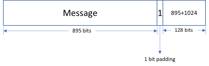
When the message size is 895 bits, a padding of ‘1’ is also considered valid, followed by the message size.
Figure: Multi block message

Messages with a length greater than 1024 bits are broken down into N 1024-bit blocks. The last block contains padding and the size of the message.
Hashing
The HMAC512 core performs the sha2-512 function to process the hash value of the given message. The algorithm processes each block of the 1024 bits from the message, using the result from the previous block. This data flow is shown in the following figure.
Figure: HMAC-SHA-512-256 data flow
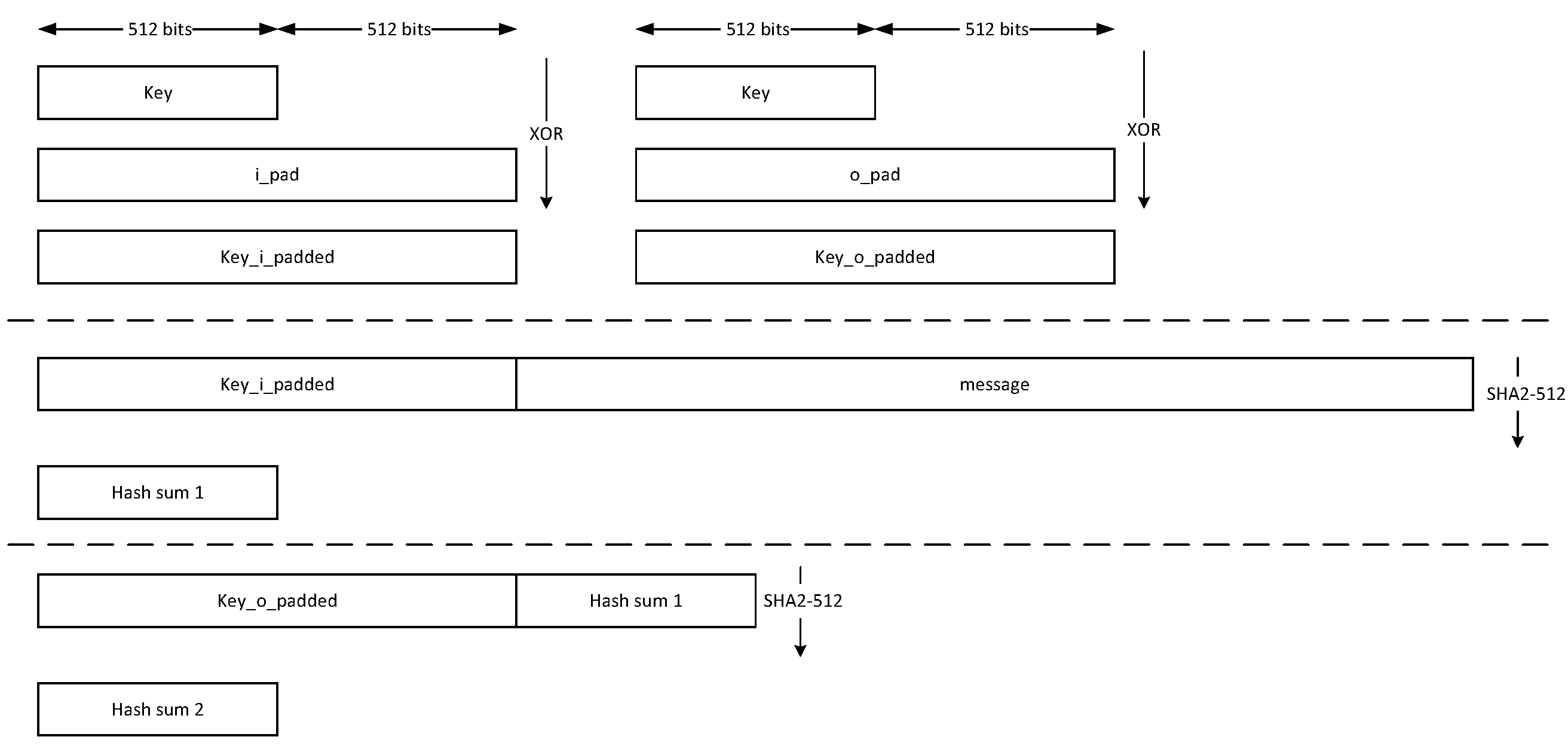
The HMAC384 core performs the sha2-384 function to process the hash value of the given message. The algorithm processes each block of the 1024 bits from the message, using the result from the previous block. This data flow is shown in the following figure.
Figure: HMAC-SHA-384-192 data flow
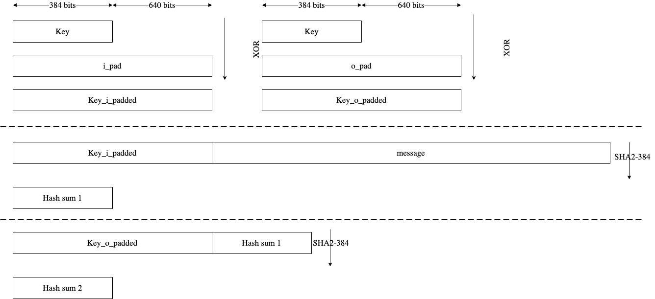
FSM
The HMAC architecture has the finite-state machine as shown in the following figure.
Figure: HMAC FSM
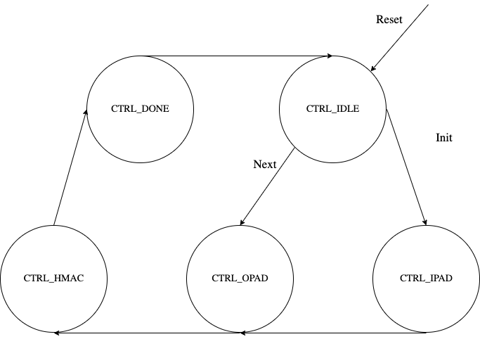
CSR Mode
When the CSR Mode register is set, the HMAC512 core uses the value latched from the cptra_csr_hmac_key interface pins in place of the API key register. These pins are latched internally after powergood assertion during DEVICE_MANUFACTURING lifecycle state. During debug mode operation this value is overridden with all 1's, and during any other lifecycle state it has a value of zero.
Signal descriptions
The HMAC architecture inputs and outputs are described in the following table.
| Name | Input or output | Description |
|---|---|---|
| clk | input | All signal timings are related to the rising edge of clk. |
| reset_n | input | The reset signal is active LOW and resets the core. This is the only active LOW signal. |
| init | input | The core is initialized and processes the key and the first block of the message. |
| next | input | The core processes the rest of the message blocks using the result from the previous blocks. |
| zeroize | input | The core clears all internal registers to avoid any SCA information leakage. |
| csr_mode | input | When set, the key comes from the cptra_csr_hmac_key interface pins. This key is valid only during MANUFACTURING mode. |
| mode | input | Indicates the hmac type of the function. This can be: - HMAC384 - HMAC512. |
| cptra_csr_hmac_key[511:0] | input | The key to be used during csr mode. |
| key[511:0] | input | The input key. |
| block[1023:0] | input | The input padded block of message. |
| LFSR_seed[383:0] | Input | The input to seed PRNG to enable the masking countermeasure for SCA protection. |
| ready | output | When HIGH, the signal indicates the core is ready. |
| tag[511:0] | output | The HMAC value of the given key or block. For PRF-HMAC-SHA-512, a 512-bit tag is required. For HMAC-SHA-512-256, the host is responsible for reading 256 bits from the MSB. |
| tag_valid | output | When HIGH, the signal indicates the result is ready. |
Address map
The HMAC address map is shown here: hmac_reg -- clp Reference (chipsalliance.github.io).
Pseudocode
The following pseudocode demonstrates how the HMAC interface can be implemented.
Figure: HMAC pseudocode
SCA countermeasure
In an attack model, an attacker can form hypotheses about the secret key value and compute the corresponding output values by using the Hamming Distance model as an appropriate leakage model. An attacker who has knowledge of the implementation for open-source architecture has an advantage. The attacker can capture the power consumption traces to verify their hypotheses, by partitioning the acquisitions or using Pearson’s correlation coefficient.
To protect the HMAC algorithm from side-channel attacks, a masking countermeasure is applied. This means that random values are added to the intermediate variables during the algorithm’s execution, so that the side-channel signals do not reveal any information about them.
The embedded countermeasures are based on "Differential Power Analysis of HMAC Based on SHA-2, and Countermeasures" by McEvoy et. al. To provide the required random values for masking intermediate values, a lightweight 74-bit LFSR is implemented. Based on “Spin Me Right Round Rotational Symmetry for FPGA-specific AES” by Wegener et. al., LFSR is sufficient for masking statistical randomness.
Each round of SHA512 execution needs 6,432 random bits, while one HMAC operation needs at least 4 rounds of SHA512 operations. However, the proposed architecture requires only 384-bit LFSR seed and provides first-order DPA attack protection at the cost of 10% latency overhead with negligible hardware resource overhead.
Performance
The HMAC core performance is reported considering two different architectures: pure hardware architecture, and hardware/software architecture. These are described next.
Pure hardware architecture
In this architecture, the HMAC interface and controller are implemented in hardware. The performance specification of the HMAC architecture is reported as shown in the following table.
| Operation | Cycle count [CCs] | Time [us] @ 400 MHz | Throughput [op/s] |
|---|---|---|---|
| Data_In transmission | 44 | 0.11 | - |
| Process | 254 | 0.635 | - |
| Data_Out transmission | 12 | 0.03 | - |
| Single block | 310 | 0.775 | 1,290,322 |
| Double block | 513 | 1.282 | 780,031 |
| 1 KiB message | 1,731 | 4.327 | 231,107 |
| 128 KiB message | 207,979 | 519.947 | 1,923 |
Hardware/software architecture
In this architecture, the HMAC interface and controller are implemented in RISC-V core. The performance specification of the HMAC architecture is reported as shown in the following table.
| Operation | Cycle count [CCs] | Time [us] @ 400 MHz | Throughput [op/s] |
|---|---|---|---|
| Data_In transmission | 1389 | 3.473 | - |
| Process | 253 | 0.633 | - |
| Data_Out transmission | 290 | 0.725 | - |
| Single block | 1932 | 4.83 | 207,039 |
| Double block | 3166 | 7.915 | 136,342 |
| 1 KiB message | 10,570 | 26.425 | 37,842 |
| 128 KiB message | 1,264,314 | 3,160.785 | 316 |
HMAC_DRBG
Hash-based message authentication code (HMAC) deterministic random bit generator (DRBG) is a cryptographic random bit generator that uses a HMAC function. HMAC_DRBG involves a cryptographic HMAC function and a seed. This architecture is designed as specified in section 10.1.2. of NIST SP 800-90A [12]. For ECC signing operation, the implementation is compatible with section 3.1. of RFC 6979 [7].
Caliptra HMAC_DRBG implementation uses HMAC384 as the HMAC function, accepts a 384-bit seed, and generates a 384-bit random value.
The HMAC algorithm is described as follows:
- The seed is fed to HMAC_DRBG core by the host
- For each 384-bit random value
- The core should be triggered by the host
- The HMAC_DRBG core status is changed to ready after HMAC processing
- The result digest can be read
Operation
HMAC_DRBG uses a loop of HMAC(K, V) to generate the random bits. In this algorithm, two constant values of K_init and V_init are used as follows:
        1. 	Set V_init = 0x01 0x01 0x01 ... 0x01  (V has 384-bit)
        2. 	Set K_init = 0x00 0x00 0x00 ... 0x00  (K has 384-bit)
        3. 	K_tmp = HMAC(K_init, V_init || 0x00 || entropy || nonce)
        4. 	V_tmp = HMAC(K_tmp,  V_init)
        5. 	K_new = HMAC(K_tmp,  V_tmp  || 0x01 || entropy || nonce)
        6. 	V_new = HMAC(K_new,  V_tmp)
        7. 	Set T = []
        8. 	T = T || HMAC(K_new, V_new)
        9. 	Return T if T is within the [1,q-1] range, otherwise:
        10.	K_new = HMAC(K_new,  V_new || 0x00)
        11.	V_new = HMAC(K_new,  V_new)
        12.	Jump to 8
For ECC KeyGen operation, HMAC_DRBG is used to generate privkey as follows:
Privkey = HMAC_DRBG(seed, nonce)
For ECC SIGNING operation, HMAC_DRBG is used to generate k as follows:
K = HMAC_DRBG(privkey, hashed_msg)
Signal descriptions
The HMAC_DRBG architecture inputs and outputs are described in the following table.
| Name | Input or output | Description |
|---|---|---|
| clk | input | All signal timings are related to the rising edge of clk. |
| reset_n | input | The reset signal is active LOW and resets the core. This is the only active LOW signal. |
| init | input | The core is initialized with the given seed and generates a 384-bit random value. |
| next | input | The core generates a new 384-bit random value using the result from the previous run. |
| zeroize | input | The core clears all internal registers to avoid any SCA information leakage. |
| entropy [383:0] | input | The input entropy. |
| nonce [383:0] | input | The input nonce. |
| LFSR_seed [147 :0] | input | The input to seed PRNG to enable masking countermeasure for SCA protection. |
| ready | output | When HIGH, the signal indicates the core is ready. |
| drbg [383:0] | output | The hmac_drbg value of the given inputs. |
| valid | output | When HIGH, the signal indicates the result is ready. |
Address map
The HMAC_DRBG is embedded into ECC architecture, since there is no address map to access it from FW.
SCA countermeasure
For information, see SCA countermeasure in the HMAC384 section.
ECC
The ECC unit includes the ECDSA (Elliptic Curve Digital Signature Algorithm) engine and the ECDH (Elliptic Curve Diffie-Hellman Key-Exchange) engine, offering a variant of the cryptographically secure Digital Signature Algorithm (DSA) and Diffie-Hellman Key-Exchange (DH), which uses elliptic curve (ECC). A digital signature is an authentication method in which a public key pair and a digital certificate are used as a signature to verify the identity of a recipient or sender of information.
The hardware implementation supports deterministic ECDSA, 384 Bits (Prime Field), also known as NIST-Secp384r1, described in RFC6979.
The hardware implementation also supports ECDH, 384 Bits (Prime Field), also known as NIST-Secp384r1, described in SP800-56A.
Secp384r1 parameters are shown in the following figure.
Figure: Secp384r1 parameters
Operation
The ECDSA consists of three operations, shown in the following figure.
Figure: ECDSA operations
The ECDH also consists of the sharedkey generation.
KeyGen
In the deterministic key generation, the paired key of (privKey, pubKey) is generated by KeyGen(seed, nonce), taking a deterministic seed and nonce. The KeyGen algorithm is as follows:
- Compute privKey = HMAC_DRBG(seed, nonce) to generate a random integer in the interval [1, n-1] where n is the group order of Secp384 curve.
- Generate pubKey(x,y) as a point on ECC calculated by pubKey=privKey × G, while G is the generator point over the curve.
Signing
In the signing algorithm, a signature (r, s) is generated by Sign(privKey, h), taking a privKey and hash of message m, h = hash(m), using a cryptographic hash function, SHA512. The signing algorithm includes:
- Generate a random number k in the range [1..n-1], while k = HMAC_DRBG(privKey, h)
- Calculate the random point R = k × G
- Take r = Rx mod n, where Rx is x coordinate of R=(Rx, Ry)
- Calculate the signature proof: s = k-1 × (h + r × privKey) mod n
- Return the signature (r, s), each in the range [1..n-1]
Verifying
The signature (r, s) can be verified by Verify(pubKey ,h ,r, s) considering the public key pubKey and hash of message m, h=hash(m) using the same cryptographic hash function SHA512. The output is r’ value of verifying a signature. The ECDSA verify algorithm includes:
- Calculate s1 = s−1 mod n
- Compute R' = (h × s1) × G + (r × s1) × pubKey
- Take r’ = R'x mod n, while R'x is x coordinate of R’=(R'x, R'y)
- Verify the signature by comparing whether r' == r
ECDH sharedkey
In ECDH sharedkey generation, the shared key is generated by ECDH_sharedkey(privKey_A, pubKey_B), taking an own prikey and other party pubkey. The ECDH sharedkey algorithm is as follows:
- Compute P = sharedkey(privkey_A, pubkey_b) where P(x,y) is a point on ECC.
- Output sharedkey = Px, where Px is x coordinate of P.
Architecture
The ECC top-level architecture is shown in the following figure.
Figure: ECC architecture
Signal descriptions
The ECC architecture inputs and outputs are described in the following table.
| Name | Input or output | Description |
|---|---|---|
| clk | input | All signal timings are related to the rising edge of clk. |
| reset_n | input | The reset signal is active LOW and resets the core. This is the only active LOW signal. |
| ctrl[1:0] | input | Indicates the AES type of the function. This can be: − 0b00: No Operation − 0b01: KeyGen − 0b10: Signing − 0b11: Verifying |
| zeroize | input | The core clears all internal registers to avoid any SCA information leakage. |
| seed [383:0] | input | The deterministic seed for HMAC_DRBG in the KeyGen operation. |
| nonce [383:0] | input | The deterministic nonce for HMAC_DRBG in the KeyGen operation. |
| privKey_in[383:0] | input | The input private key used in the signing operation. |
| pubKey_in[1:0][383:0] | input | The input public key(x,y) used in the verifying operation. |
| hashed_msg[383:0] | input | The hash of message using SHA512. |
| ready | output | When HIGH, the signal indicates the core is ready. |
| privKey_out[383:0] | output | The generated private key in the KeyGen operation. |
| pubKey_out[1:0][383:0] | output | The generated public key(x,y) in the KeyGen operation. |
| r[383:0] | output | The signature value of the given priveKey/message. |
| s[383:0] | output | The signature value of the given priveKey/message. |
| r’[383:0] | Output | The signature verification result. |
| DH_sharedkey[383:0] | output | The generated shared key in the ECDH sharedkey operation. |
| valid | output | When HIGH, the signal indicates the result is ready. |
Address map
The ECC address map is shown here: ecc_reg -- clp Reference (chipsalliance.github.io).
Pseudocode
The following pseudocode blocks demonstrate example implementations for KeyGen, Signing, Verifying, and ECDH sharedkey.
KeyGen
Figure: KeyGen pseudocode
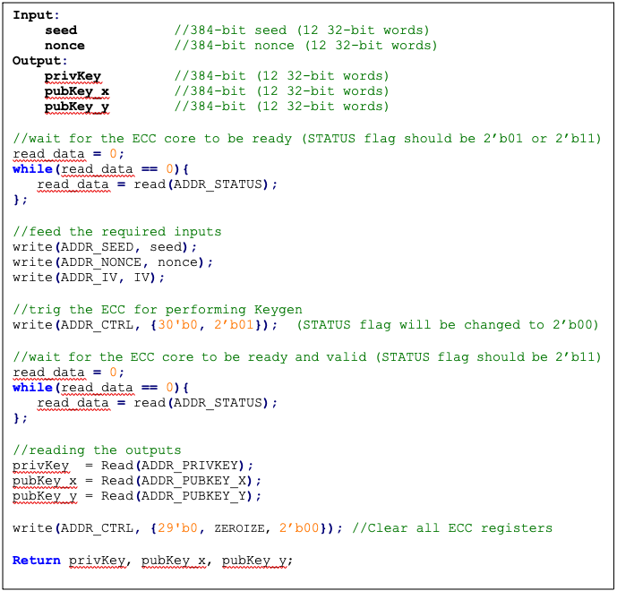
Signing
Figure: Signing pseudocode
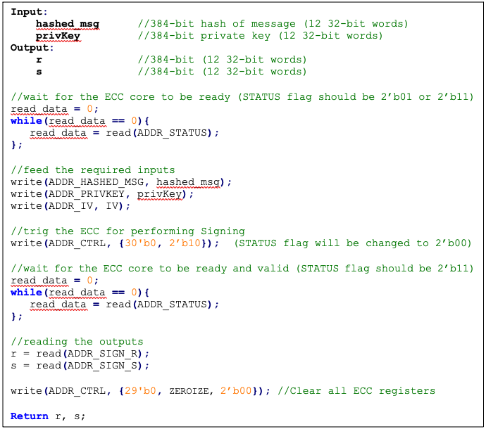
Verifying
Figure: Verifying pseudocode
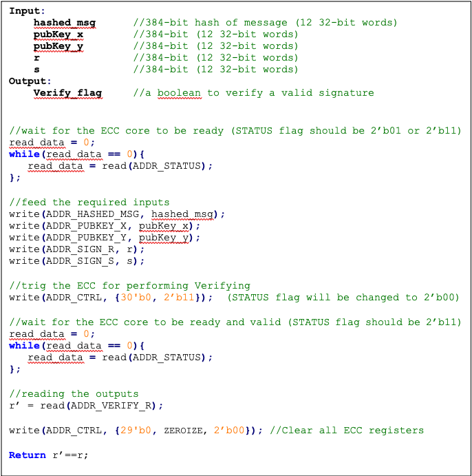
ECDH sharedkey
Figure: ECDH sharedkey pseudocode
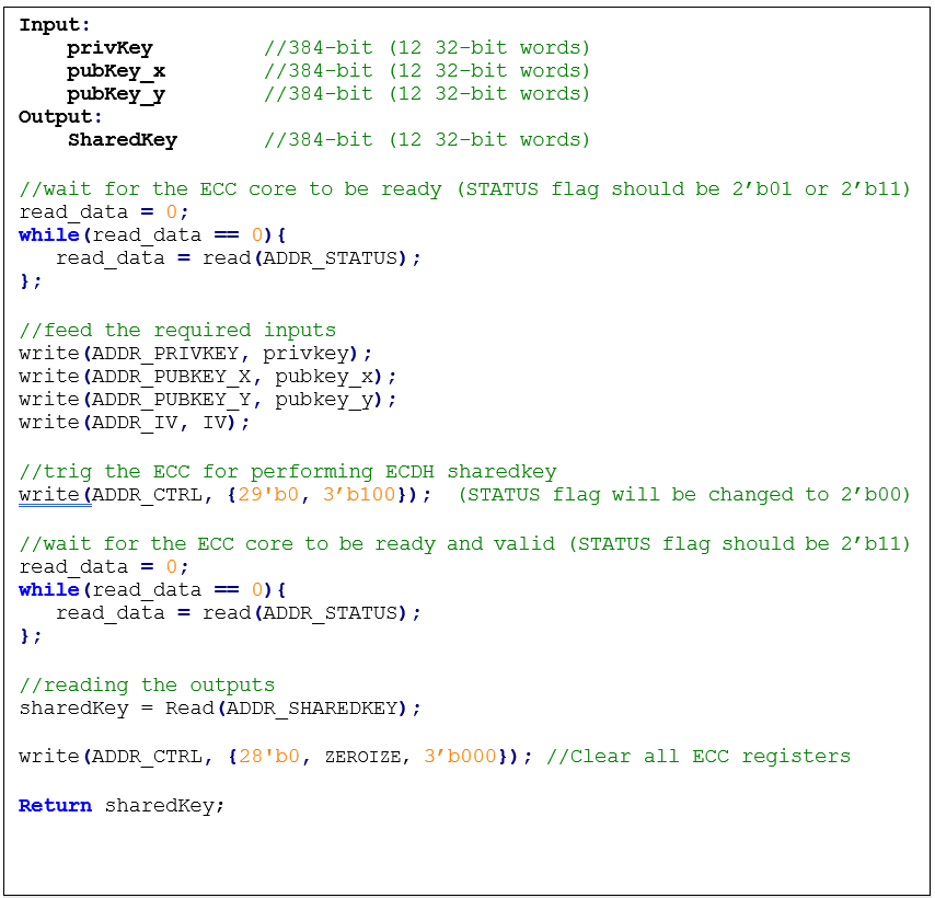
SCA countermeasure
The described ECC has four main routines: KeyGen, Signing, Verifying, and ECDH sharedkey. Since the Verifying routine requires operation with public values rather than a secret value, our side-channel analysis does not cover this routine. Our evaluation covers the KeyGen, Signing, and ECDH sharedkey routines where the secret values are processed.
KeyGen consists of HMAC DRBG and scalar multiplication, while Signing first requires a message hashing and then follows the same operations as KeyGen (HMAC DRBG and scalar multiplication). The last step of Signing is generating “S” as the proof of signature. Since HMAC DRBG and hash operations are evaluated separately in our document, this evaluation covers scalar multiplication and modular arithmetic operations.
Scalar multiplication
To perform the scalar multiplication, the Montgomery ladder is implemented, which is inherently resistant to timing and single power analysis (SPA) attacks.
Implementation of complete unified addition formula for the scalar multiplication avoids information leakage and enhances architecture from security and mathematical perspectives.
To protect the architecture against horizontal power/electromagnetic (EM) and differential power analysis (DPA) attacks, several countermeasures are embedded in the design [9]. Since these countermeasures require random inputs, HMAC-DRBG is fed by IV to generate these random values.
Since HMAC-DRBG generates random value in a deterministic way, firmware MUST feed different IV to ECC engine for EACH keygen, signing, and ECDH sharedkey operation.
Base point randomization
This countermeasure is achieved using the randomized base point in projective coordinates. Hence, the base point G=(Gx, Gy) in affine coordinates is transformed and randomized to projective coordinates as (X, Y, Z) using a random value as follows:
This approach does not have the performance or area overhead because the architecture is variable-base-point implemented.
Scalar blinding
This countermeasure is achieved by randomizing the scalar as follows:
Based on [10], half of the bit size of is required to prevent advanced DPA attacks. Therefore, has 192 bits, and the blinded scalar has 576 bits. Hence, this countermeasure extends the Montgomery ladder iterations due to extended scalar.
This approach is achieved at the cost of 50% more latency on scalar multiplication and adding one lightweight block, including one 32*32 multiplier and an accumulator.
Note: the length of rand is configurable to have a trade-off between the required protection and performance.
Making countermeasures embedded into HMAC_DRBG
In the first step of the KeyGen operation, the privkey is generated using HMAC_DRBG by feeding the following two inputs: seed and nonce. To avoid SCA information leakage during this operation, we embed masking countermeasures into the HMAC_DRBG architecture.
Each round of SHA512 execution needs 6,432 random bits, and one HMAC operation needs at least 4 rounds of SHA512 operations. Furthermore, each HMAC_DRBG round needs at least 5 rounds of HMAC operations. However, the proposed architecture uses a lightweight LFSR and provides first-order DPA attack protection with negligible latency and hardware resource overhead.
ECDSA signing nonce leakage
Generating “S” as the proof of signature at the steps of the signing operation leaks where the hashed message is signed with private key and ephemeral key as follows:
Since the given message is known or the signature part r is known, the attacker can perform a known-plaintext attack. The attacker can sign multiple messages with the same key, or the attacker can observe part of the signature that is generated with multiple messages but the same key.
The evaluation shows that the CPA attack can be performed with a small number of traces, respectively. Thus, an arithmetic masked design for these operations is implemented.
Masking signature
This countermeasure is achieved by randomizing the privkey as follows:
Although computation of “S” seems the most vulnerable point in our scheme, the operation does not have a big contribution to overall latency. Hence, masking these operations has low overhead on the cost of the design.
Random number generator for SCA countermeasure
The ECC countermeasure requires several random vectors to randomize the intermediate values, as described in the preceding section. HMAC_DRBG is used to take one random vector of 384-bit (i.e., ECC_IV register) and to generate the required random vectors for different countermeasures.
The state machine of HMAC_DRBG utilization is shown in the following figure, including three main states:
- SCA random generator: Running HMAC_DRBG with IV and an internal counter to generate the required random vectors.
- KEYGEN PRIVKEY: Running HMAC_DRBG with seed and nonce to generate the privkey in KEYGEN operation.
- SIGNING NONCE: Running HMAC_DRBG based on RFC6979 in SIGNING operation with privkey and hashed_msg.
Figure: HMAC_DRBG utilization
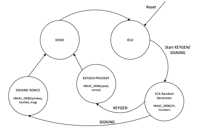
In SCA random generator state:
- This state (in KeyGen operation mode) generates 3 384-bit random vectors for the following: LFSR, base point randomization, and scalar blinding randomization.
- This state (in signing operation) generates 4 384-bit random vectors for the following: LFSR, base point randomization, scalar blinding, and masking signature randomization.
- HMAC_DRBG is initialized with IV and an internal counter. This 64-bit counter enables after reset and zeroization and contains different values depending on when ECC is called.
- HMAC_DRBG is enabled by the INIT command. To generate all required vectors, HMAC-DRBG is continued by the NEXT command that increments the built-in counter inside the HMAC-DRBG unit.
- To initialize the required seed for LFSR, LFSR_INIT_SEED is set as a constant by RTL after reset and zeroization. However, this value is updated before enabling HMAC_DRBG as follows:
- In the first execution of HMAC_DRBG after reset and zeroization, hmac_lfsr_seed is equal to LFSR_INIT_SEED XORed by internal 64-bit counter.
- In the next executions of HMAC_DRBG, hmac_lfsr_seed is equal to HMAC_DRBG output of the first execution XORed by internal 64-bit counter.
The data flow of the HMAC_DRBG operation in keygen operation mode is shown in the following figure.
Figure: HMAC_DRBG data flow
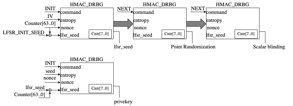
TVLA results
Test vector leakage assessment (TVLA) provides a robust test using a 𝑡-test. This test evaluates the differences between sets of acquisitions to determine if one set of measurement can be distinguished from the other. This technique can detect different types of leakages, providing a clear indication of leakage or lack thereof.
In practice, observing a t-value greater than a specific threshold (mainly 4.5) indicates the presence of leakage. However, in ECC, due to its latency, around 5 million samples are required to be captured. This latency leads to many false positives and the TVLA threshold can be considered a higher value than 4.5. Based on the following figure from “Side-Channel Analysis and Countermeasure Design for Implementation of Curve448 on Cortex-M4” by Bisheh-Niasar et. al., the threshold can be considered equal to 7 in our case.
Figure: TVLA threshold as a function of the number of samples per trace
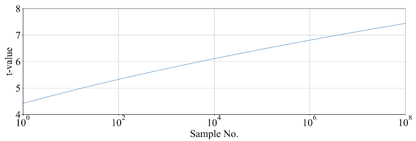
KeyGen TVLA
The TVLA results for performing seed/nonce-dependent leakage detection using 200,000 traces is shown in the following figure. Based on this figure, there is no leakage in ECC keygen by changing the seed/nonce after 200,000 operations.
Figure: seed/nonce-dependent leakage detection using TVLA for ECC keygen after 200,000 traces
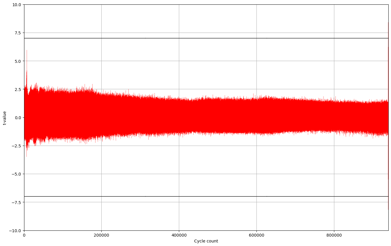
Signing TVLA
The TVLA results for performing privkey-dependent leakage detection using 20,000 traces is shown in the following figure. Based on this figure, there is no leakage in ECC signing by changing the privkey after 20,000 operations.
Figure: privkey-dependent leakage detection using TVLA for ECC signing after 20,000 traces
The TVLA results for performing message-dependent leakage detection using 64,000 traces is shown in the following figure. Based on this figure, there is no leakage in ECC signing by changing the message after 64,000 operations.
Figure: Message-dependent leakage detection using TVLA for ECC signing after 64,000 traces
The point with t-value equal to -40 is mapped to the Montgomery conversion of the message that is a publicly known value (no secret is there). By ignoring those corresponding samples, there are some sparse samples with a t-value greater than 7, as shown in the following table.
| Sample | Duration | Cycle | t-value | Operation |
|---|---|---|---|---|
| 4,746,127 | 214 | 911,381.4 | 11.2 | start of mont_conv(msg) |
| 4,746,341 | 911,422.5 | -40 | end of mont_conv(msg) | |
| 4,757,797 | 1 | 913,622.0 | 7.4 | inv_q |
| 4,768,302 | 1 | 915,639.0 | 7.8 | inv_q |
| 4,779,610 | 1 | 917,810.1 | -9.1 | inv_q |
| 4,788,120 | 1 | 919,444.0 | 7.6 | inv_q |
| 4,813,995 | 1 | 924,412.0 | 7.3 | inv_q |
| 4,822,693 | 1 | 926,082.1 | 7.5 | inv_q |
| 4,858,671 | to the end | 932,989.8 | -7.6 | Ended ECC signing |
Performance
The ECC core performance is reported in the next section.
Pure hardware architecture
In this architecture, the ECC interface and controller are implemented in hardware. The performance specification of the ECC architecture is reported as shown in the following table.
| Operation | Cycle count [CCs] | Time [ms] @ 400 MHz | Throughput [op/s] |
|---|---|---|---|
| Keygen | 909,648 | 2.274 | 439 |
| Signing | 932,990 | 2.332 | 428 |
| Verifying | 1,223,938 | 3.060 | 326 |
LMS Accelerator
LMS cryptography is a type of hash-based digital signature scheme that was standardized by NIST in 2020. It is based on the Leighton-Micali Signature (LMS) system, which uses a Merkle tree structure to combine many one-time signature (OTS) keys into a single public key. LMS cryptography is resistant to quantum attacks and can achieve a high level of security without relying on large integer mathematics.
Caliptra supports only LMS verification using a software/hardware co-design approach. Hence, the LMS accelerator reuses the SHA256 engine to speedup the Winternitz chain by removing software-hardware interface overhead. The LMS-OTS verification algorithm is shown in following figure:
Figure: LMS-OTS Verification algorithm
The high-level architecture of LMS is shown in the following figure.
Figure: LMS high-level architecture
LMS parameters
LMS parameters are shown in the following table:
| Parameter | Description | Value |
|---|---|---|
| n | The number of bytes of the output of the hash function. | {24, 32} |
| w | The width (in bits) of the Winternitz coefficients. | {1, 2, 4, 8} |
| p | The number of n-byte string elements that make up the LM-OTS signature. | {265, 133, 67, 34} |
| H | A cryptographic hash function. | SHA256 |
| h | The height of the tree. | {5, 10, 15, 20, 25} |
- SHA256 is used for n=32 and SHA256/192 is used for n=24.
- SHAKE256 is not supported in this architecture.
- Value of p is determined based on w. If w=1, p is equal to 265, and so on.
Winternitz Chain Accelerator
The Winternitz hash chain can be accelerated in hardware to enhance the performance of the design. For that, a configurable architecture is proposed that can reuse SHA256 engine. The LMS accelerator architecture is shown in the following figure, while H is SHA256 engine.
Figure: Winternitz chain architecture
Signal descriptions
The LMS accelerator integrated into SHA256 architecture inputs and outputs are described as follows.
| Name | Input or output | Description |
|---|---|---|
| clk | input | All signal timings are related to the rising edge of clk. |
| reset_n | input | The reset signal is active LOW and resets the core. This is the only active LOW signal. |
| init | input | The core is initialized and processes the first block of message. |
| next | input | The core processes the rest of the message blocks using the result from the previous blocks. |
| mode | input | Indicates the hash type of the function. This can be: - SHA256/224 - SHA256 |
| zeroize | input | The core clears all internal registers to avoid any SCA information leakage. |
| WNTZ_MODE | input | SHA256 core is configured in Winternitz verification mode. |
| WNTZ_W[3:0] | input | Winternitz W value. |
| WNTZ_N_MODE | input | Winternitz n value(SHA192/SHA256 --> n = 24/32) |
| block[511:0] | input | The input padded block of message. |
| ready | output | When HIGH, the signal indicates the core is ready. |
| digest[255:0] | output | The hashed value of the given block. |
| digest_valid | output | When HIGH, the signal indicates the result is ready. |
Address map
The address map for LMS accelerator integrated into SHA256 is shown here: sha256_reg -- clp Reference (chipsalliance.github.io).
Adams Bridge - Dilithium (ML-DSA)
Please refer to the Adams-bridge specification
Address map
Address map of ML-DSA accelerator is shown here: ML-DSA_reg -- clp Reference (chipsalliance.github.io)
Adams Bridge Kyber ML-KEM
Please refer to the Adams-bridge specification
Address map
Address map of ML-KEM accelerator is shown here: ML-KEM_reg -- clp Reference (chipsalliance.github.io)
AES
The AES unit is a cryptographic accelerator that processes requests from the processor to encrypt or decrypt 16-byte data blocks. It supports AES-128/192/256 in various modes, including Electronic Codebook (ECB), Cipher Block Chaining (CBC), Cipher Feedback (CFB) with a fixed segment size of 128 bits (CFB-128), Output Feedback (OFB), Counter (CTR), and Galois/Counter Mode (GCM).
The AES unit is reused from here, (see aes with a shim to translate from AHB-lite to the tl-ul interface.
Additional registers have been added to support key vault integration. Keys from the key vault can be loaded into the AES unit to be used for encryption or decryption.
Operation
For more information, see the AES Programmer's Guide.
AES Endian
The AES Core uses little endian for the DATA_IN and DATA_OUT registers. Caliptra allows a user to stream the data into and out of AES in big endian when AES_CLP.CTRL0.ENDIAN_SWAP is set to 1. This is done by swizzling the write and read data when a write targets DATA_IN or a read targets DATA_OUT.
By default little endian is selected.
Signal descriptions
The AES architecture inputs and outputs are described in the following table.
| Name | Input or output | Description |
|---|---|---|
| clk | input | All signal timings are related to the rising edge of clk. |
| reset_n | input | The reset signal is active LOW and resets the core. This is the only active LOW signal. |
| DATA_IN | input | Input block to be encrypted or decrypted. Written in four 32-bit registers. |
| DATA_OUT | output | Output block result of encryption or decryption. Stored in four 32-bit registers. |
| CTRL_SHADOWED.MANUAL_OPERATION | input | Configures the AES core to operation in manual mode. |
| CTRL_SHADOWED.PRNG_RESEED_RATE | input | Configures the rate of reseeding the internal PRNG used for masking. |
| CTRL_SHADOWED.SIDELOAD | input | When asserted, AES core will use the key from the key vault interface. |
| CTRL_SHADOWED.KEY_LEN | input | Configures the AES key length. Supports 128, 192, and 256-bit keys. |
| CTRL_SHADOWED.MODE | input | Configures the AES block cipher mode. |
| CTRL_SHADOWED.OPERATION | input | Configures the AES core to operate in encryption or decryption modes. |
| CTRL_GCM_SHADOWED.PHASE | input | Configures the GCM phase. |
| CTRL_GCM_SHADOWED.NUM_VALID_BYTES | input | Configures the number of valid bytes of the current input block in GCM. |
| TRIGGER.PRNG_RESEED | input | Forces a PRNG reseed. |
| TRIGGER.DATA_OUT_CLEAR | input | Clears the DATA_OUT registers with pseudo-random data. |
| TRIGGER.KEY_IV_DATA_IN_CLEAR | input | Clears the Key, IV, and DATA_INT registers with pseudo-random data. |
| TRIGGER.START | input | Triggers the encryption/decryption of one data block if in manual operation mode. |
| STATUS.ALERT_FATAL_FAULT | output | A fatal fault has ocurred and the AES unit needs to be reset. |
| STATUS.ALERT_RECOV_CTRL_UPDATE_ERR | output | An update error has occurred in the shadowed Control Register. AES operation needs to be restarted by re-writing the Control Register. |
| STATUS.INPUT_READY | output | The AES unit is ready to receive new data input via the DATA_IN registers. |
| STATUS.OUTPUT_VALID | output | The AES unit has alid output data. |
| STATUS.OUTPUT_LOST | output | All previous output data has been fully read by the processor (0) or at least one previous output data block has been lost (1). It has been overwritten by the AES unit before the processor could fully read it. Once set to 1, this flag remains set until AES operation is restarted by re-writing the Control Register. The primary use of this flag is for design verification. This flag is not meaningful if MANUAL_OPERATION=0. |
| STATUS.STALL | output | The AES unit is stalled because there is previous output data that must be read by the processor before the AES unit can overwrite this data. This flag is not meaningful if MANUAL_OPERATION=1. |
| STATUS.IDLE | output | The AES unit is idle. |
Address map
The AES address map is shown here: aes_clp_reg -- clp Reference (chipsalliance.github.io).
SCA countermeasures
The AES unit employs separate SCA countermeasures for the AES cipher core used for the encryption/decryption part and for the GHASH module used for computing the integrity tag in GCM.
AES cipher core
A detailed specification of the SCA countermeasure employed in the AES cipher core is shown here: AES cipher core SCA countermeasure. The most critical building block of the SCA countermeasure, i.e., the masked AES S-Box, successfully passes formal masking verification at the netlist level using Alma: Execution-aware Masking Verification. The flow required for repeating the formal masking verification using Alma together with a Howto can be found here. The entire AES cipher core including the masked S-Boxes and as well as the PRNG generating the randomness for remasking successfully passes masking evaluation at the netlist level using PROLEAD - A Probing-Based Leakage Detection Tool for Hardware and Software. The flow required for repeating the masking evaluation using PROLEAD together with a Howto can be found here.
GHASH module
A detailed specification of the SCA countermeasure employed in the GHASH module is shown here: GHASH module SCA countermeasure.
To optimize and verify this masking countermeasure, two different types of experiments have been performed for which the results are given below.
- Formal masking verification using Alma: Execution-aware Masking Verification. These experiments led to a series of small design optimizations which have been integrated into Caliptra. The resulting design successfully passes formal masking verification at the netlist level.
- Test-vector leakage assessment (TVLA) applied to power SCA traces captured on a ChipWhisperer-based FPGA setup. These experiments confirm the formal masking verification results: No 1st-order SCA can be observed during the GHASH operation. The leakage observed at the boundary of and outside the GHASH operation can be attributed to the evaluation methodology and the handling of unmasked and uncritical data, as well as to FPGA-specific leakage effects known from literature. We are confident that the optimized SCA hardening concept effectively deters SCA attacks.
Formal masking verification using Alma
Alma is an open source, formal masking verification tool developed at TU Graz which enables formal verification of masking SCA countermeasures at the netlist level. The main advantages of this approach compared to analyzing FPGA power traces are as follows:
- The turn-around time is much faster as it does not involve FPGA bitstream generation and capturing power traces (both can take several hours).
- Netlist-based analysis tools typically enable pinpointing sources of SCA leakage and easily allow analyzing sub parts of the masked design individually. As a result, individual issues can be fixed up faster.
- The analyzed netlist is closer to the targeted ASIC implementation. During FPGA synthesis, the netlist is mapped to the logic elements such as look-up tables (LUTs) available on the selected FPGA which are fundamentally different from more simple ASIC gates.
However, formal netlist analysis tools may not be perfect and they also have limitations in terms of what can be analyzed. For example, the maximum supported netlist size depends on the complexity and number of the non-linear elements. Also, random number generators and in particular pseudo-random number generators typically need to be excluded from the analysis and random number inputs need to be assumed as ideal by tools. Thus, they don’t replace FPGA-based analysis. We use them to increase our confidence in our SCA countermeasures and to close countermeasure verification faster by reducing the number of FPGA evaluation runs.
Prerequisites
The Alma-based formal masking verification flow together with a Howto (including installation instructions) as well an open source Yosys synthesis flow are available open soure. The tool can both run on generic Yosys netlists or on proprietary and technology-specific netlists. For the latter, a slightly modified verification flow with an additional translation step is required. To verify the GHASH SCA countermeasure, the generic flow was used with the following tool versions:
- Alma (specific commit)
- Yosys 0.36 (git sha1 8f07a0d84)
- sv2v v0.0.11-28-g81d8225
- Verilator 4.214 2021-10-17 rev v4.214
Yosys Netlist Synthesis
Setup the open source Yosys synthesis flow by copying the syn_setup.example.sh file and renaming it to syn_setup.sh.
Change the LR_SYNTH_TOP_MODULE variable to aes_ghash_wrap and the LR_SYNTH_CELL_LIBRARY_PATH to the NangateOpenCellLibrary_typical.lib file in the folder where you installed the nangate45 library.
Then, start the synthesis by executing
./syn_yosys.sh
This should produce output similar to what is shown below:
8. Printing statistics.

=== aes_ghash_wrap ===

   Number of wires:             24543
   Number of wire bits:         29339
   Number of public wires:      567
   Number of public wire bits:  5363
   Number of memories:          0
   Number of memory bits:       0
   Number of processes:         0
   Number of cells:             26214
    AND2_X1                     1585
    AND3_X1                     4
    AND4_X1                     32
    AOI211_X1                   58
    AOI21_X1                    293
    AOI221_X1                   215
    AOI22_X1                    364
    DFFR_X1                     1468
    DFFS_X1                     5
    INV_X1                      584
    MUX2_X1                     1252
    NAND2_X1                    1870
    NAND3_X1                    128
    NAND4_X1                    37
    NOR2_X1                     7551
    NOR3_X1                     445
    NOR4_X1                     28
    OAI211_X1                   98
    OAI21_X1                    827
    OAI221_X1                   3
    OAI22_X1                    183
    OR2_X1                      28
    OR3_X1                      67
    OR4_X1                      2
    XNOR2_X1                    7122
    XOR2_X1                     1965

   Chip area for module '\aes_ghash_wrap': 37534.728000

====== End Yosys Stat Report ======

Warnings: 20 unique messages, 102 total

End of script. Logfile hash: 16c4d13569, CPU: user 25.11s system 0.12s, MEM: 176.29 MB peak
Yosys 0.36 (git sha1 8f07a0d84, gcc 11.4.0-1ubuntu1~22.04 -fPIC -Os)
Time spent: 66% 2x abc (47 sec), 9% 40x opt_expr (6 sec), ...
Area in kGE =  47.04
Note that the reported area is quite a bit bigger compared to the number reported in the GHASH SCA countermeasure specification The reasons are twofold:
- The
aes_ghash_wrapmodule synthesized is a wrapper module around the GHASH module in focus of this analysis. The goal of the wrapper is to separately feed in secrets (the hash subkey H and the encrypted initial counter block S) as well as randomness in a tool aware manner. As such, the wrapper includes some additional muxing resources and a counter to ease interpretation of results. - To speed up the formal analysis, the pipelined Galois-field multipliers have been instantiated with a latency of 4 instead of 32 clock cycles as on FPGA. While the latency or more precisely the processing parallelism does have an impact on the SNR, it does not have an impact on the formal netlist analysis which is performed in a so-to-say noise free environment.
Formal Netlist Analysis
After synthesizing the netlist, the following steps should be taken to perform the analysis:
-
Make sure to source the
build_consts.shscriptsource util/build_consts.shin order to set up some shell variables.
-
Enter the directory where you have downloaded Alma and load the virtual Python environment
source dev/bin/activate -
Launch the Alma tool to parse, trace (simulate) and formally verify the netlist. For simplicity, a single script is provided to launch all the required steps with a single command. Simply run
${REPO_TOP}/hw/ip/aes/pre_sca/alma/verify_aes_ghash.shThis should produce output similar to the one below:
Verifying aes_ghash_wrap using Alma
Starting yosys synthesis...
| CircuitGraph | Total: 29882 | Linear: 9091 | Non-linear: 12741 | Registers: 1473 | Mux: 3538 |
parse.py successful (47.99s)
1: Running verilator on given netlist
2: Compiling verilated netlist library
3: Compiling provided verilator testbench
4: Simulating circuit and generating VCD
| CircuitGraph | Total: 29882 | Linear: 9091 | Non-linear: 12741 | Registers: 1473 | Mux: 3538 |
tmp/tmp.vcd:24765: [WARNING] Entry for name alert_fatal_i already exists in namemap (alert_fatal_i -> Ce")
tmp/tmp.vcd:24766: [WARNING] Entry for name alert_o already exists in namemap (alert_o -> De")
tmp/tmp.vcd:24767: [WARNING] Entry for name clear_i already exists in namemap (clear_i -> Ee")
tmp/tmp.vcd:24768: [WARNING] Entry for name clk_i already exists in namemap (clk_i -> Fe")
tmp/tmp.vcd:24770: [WARNING] Entry for name cyc_ctr_o already exists in namemap (cyc_ctr_o -> Ge")
tmp/tmp.vcd:24771: [WARNING] Entry for name data_in_prev_i already exists in namemap (data_in_prev_i -> He")
tmp/tmp.vcd:24772: [WARNING] Entry for name data_out_i already exists in namemap (data_out_i -> Le")
tmp/tmp.vcd:24773: [WARNING] Entry for name first_block_o already exists in namemap (first_block_o -> Pe")
tmp/tmp.vcd:24774: [WARNING] Entry for name gcm_phase_i already exists in namemap (gcm_phase_i -> Qe")
tmp/tmp.vcd:24775: [WARNING] Entry for name ghash_state_done_o already exists in namemap (ghash_state_done_o -> Re")
tmp/tmp.vcd:24776: [WARNING] Entry for name hash_subkey_i already exists in namemap (hash_subkey_i -> Ve")
tmp/tmp.vcd:24777: [WARNING] Entry for name in_ready_o already exists in namemap (in_ready_o -> ^e")
tmp/tmp.vcd:24778: [WARNING] Entry for name in_valid_i already exists in namemap (in_valid_i -> _e")
tmp/tmp.vcd:24779: [WARNING] Entry for name load_hash_subkey_i already exists in namemap (load_hash_subkey_i -> `e")
tmp/tmp.vcd:24780: [WARNING] Entry for name num_valid_bytes_i already exists in namemap (num_valid_bytes_i -> ae")
tmp/tmp.vcd:24781: [WARNING] Entry for name op_i already exists in namemap (op_i -> be")
tmp/tmp.vcd:24782: [WARNING] Entry for name out_ready_i already exists in namemap (out_ready_i -> ce")
tmp/tmp.vcd:24783: [WARNING] Entry for name out_valid_o already exists in namemap (out_valid_o -> de")
tmp/tmp.vcd:24784: [WARNING] Entry for name prd_i already exists in namemap (prd_i -> ee")
tmp/tmp.vcd:24785: [WARNING] Entry for name rst_ni already exists in namemap (rst_ni -> me")
tmp/tmp.vcd:24786: [WARNING] Entry for name s_i already exists in namemap (s_i -> ne")
0
0
Building formula for cycle 0: vars 0 clauses 0
Checking cycle 0:
Building formula for cycle 1: vars 1024 clauses 1536
Checking cycle 1:
Building formula for cycle 2: vars 3968 clauses 6528
Checking cycle 2:
Building formula for cycle 3: vars 6298 clauses 11026
Checking cycle 3:
Building formula for cycle 4: vars 14888 clauses 34886
Checking cycle 4:
Building formula for cycle 5: vars 20924 clauses 52734
Checking cycle 5:
Building formula for cycle 6: vars 53986 clauses 143674
Checking cycle 6:
Building formula for cycle 7: vars 57570 clauses 150970
Checking cycle 7:
Building formula for cycle 8: vars 80484 clauses 169282
Checking cycle 8:
Building formula for cycle 9: vars 213770 clauses 504198
Checking cycle 9:
Building formula for cycle 10: vars 594390 clauses 1617276
Checking cycle 10:
Building formula for cycle 11: vars 1024018 clauses 2881744
Checking cycle 11:
Building formula for cycle 12: vars 1704424 clauses 4910342
Checking cycle 12:
Building formula for cycle 13: vars 1713897 clauses 4915466
Checking cycle 13:
Building formula for cycle 14: vars 1834911 clauses 5233038
Checking cycle 14:
Building formula for cycle 15: vars 2258841 clauses 6492446
Checking cycle 15:
Building formula for cycle 16: vars 2734646 clauses 7907830
Checking cycle 16:
Building formula for cycle 17: vars 5868600 clauses 18374416
Checking cycle 17:
Building formula for cycle 18: vars 5922747 clauses 18524578
Checking cycle 18:
Building formula for cycle 19: vars 6100898 clauses 19061808
Checking cycle 19:
Building formula for cycle 20: vars 6427297 clauses 20074334
Checking cycle 20:
Building formula for cycle 21: vars 6949506 clauses 21693947
Checking cycle 21:
Building formula for cycle 22: vars 6949506 clauses 21693947
Checking cycle 22:
Building formula for cycle 23: vars 6949506 clauses 21693947
Checking cycle 23:
Building formula for cycle 24: vars 7057992 clauses 21994175
Checking cycle 24:
Building formula for cycle 25: vars 7407412 clauses 23047989
Checking cycle 25:
Building formula for cycle 26: vars 7797810 clauses 24221073
Checking cycle 26:
Building formula for cycle 27: vars 10939700 clauses 34732235
Checking cycle 27:
Building formula for cycle 28: vars 11268148 clauses 35780811
Checking cycle 28:
Building formula for cycle 29: vars 11268148 clauses 35780811
Checking cycle 29:
Building formula for cycle 30: vars 11268148 clauses 35780811
Checking cycle 30:
Building formula for cycle 31: vars 11376634 clauses 36081039
Checking cycle 31:
Building formula for cycle 32: vars 11726054 clauses 37134853
Checking cycle 32:
Building formula for cycle 33: vars 12116452 clauses 38307937
Checking cycle 33:
Building formula for cycle 34: vars 15258342 clauses 48819099
Checking cycle 34:
Building formula for cycle 35: vars 15586534 clauses 49867675
Checking cycle 35:
Building formula for cycle 36: vars 15619430 clauses 49965979
Checking cycle 36:
Finished in 3948.52
The execution is secure
Notes:
-
This analysis exercises the full data path of the GHASH block and comprises the following operations (controlled by a small Verilator testbench):
- Initial clearing of all internal registers.
- Loading the hash subkey H.
- Loading the encrypted initial counter block S including the subsequent generation of repeatedly used correction terms.
- Processing a first AAD/ciphertext block including the generation of a correction term that is used for the first block only.
- Processing a second AAD/ciphertext block.
- Producing the final authentication tag.
-
The following main changes have been implemented as a result of the formal netlist analysis using Alma (refer to the countermeasure spec for details):
- The result of the final addition of Share 1 of S and the unmasked GHASH state is no longer stored into the GHASH state register but directly forwarded to the output, and the state input to this addition is blanked.
The input multiplexer (
ghash_in_mux) loses one input. - The two 3-input multiplexers selecting the operands for the addition with the GHASH state (
add_in_mux) are replaced by one-hot multiplexers with registered control signals. - The Operand B inputs of both GF multipliers are now blanked. The 3-input multiplexer selecting Operand B of the second GF multiplier is replaced by a one-hot multiplexer with registered control signal. In addition, the last input slice of Operand B for this multiplier is registered. This allows the switching the multiplexer during the last clock cycle of the multiplication to avoid some undesirable transient leakage occurring upon saving the result of the multiplication into the GHASH state register (and this new value propagating through the multiplexer into the multiplier again).
- The GF multipliers are configured to output zero instead of Operand A (the hash subkey) while busy.
- The state input for the addition required for the generation of the correction term for Share 0 is blanked.
- Between adding the correction terms to the GHASH state for the last time and between unmasking the GHASH state, a bubble cycle is added to allow signals to fully settle thereby avoiding undesirable transient effects unmasking the uncorrected state shares.
- The result of the final addition of Share 1 of S and the unmasked GHASH state is no longer stored into the GHASH state register but directly forwarded to the output, and the state input to this addition is blanked.
The input multiplexer (
-
The overall area impact of these changes is low (+0.16 kGE in Yosys + nangate45).
-
The final design successfully passes the formal masking verification. For details regarding tool parameters, check the analysis script.
ChipWhisperer-based FPGA evaluation and TVLA
To underpin the results of the formal verification flow, the hardening of the GHASH module has been analyzed on the ChipWhisperer CW310 FPGA board. For this analysis, power traces with the ChipWhisperer Husky scope were captured during GCM operations. Afterwards a Test Vector Leakage Assessment (TVLA) with the ot-sca toolset has been performed. The setup is illustrated in the following Figure.
 :--:
Figure: Target CW310 FPGA board (left) and the CW Husky scope (right).
:--:
Figure: Target CW310 FPGA board (left) and the CW Husky scope (right).
Setup
 :--:
Figure: Measurement setup. The main components are the target board, the scope, and the SCA framework.
:--:
Figure: Measurement setup. The main components are the target board, the scope, and the SCA framework.
The prior Figure gives a detailed overview of the measurement setup that has been utilized to capture the power traces. The SCA evaluation framework ot-sca is the central component of the measurement setup. It is responsible for communicating with the penetration testing framework that runs on the target FPGA board and with the scope. Initially, ot-sca configures the scope (sample rate, number of samples) and the pentest framework (which input, how many encryptions, where to trigger).
Based on the configuration, the pentest framework generates the cipher input, starts the encryption, and sends back the computed tag to ot-sca. The trigger is automatically set and unset by the AES hardware block to achieve an accurate & constant trigger window. In parallel, the scope waits for the trigger, captures the power consumption, and transfers the traces to the SCA evaluation framework. The ot-sca framework stores the trace as well as the cipher configuration in a database.
 :--:
Figure: Power trace with AES encryption rounds visible (left). Aligned traces when zooming in (right).
:--:
Figure: Power trace with AES encryption rounds visible (left). Aligned traces when zooming in (right).
The prior Figure depicts power traces captured during AES-GCM encryptions with the setup above. As shown in the figure, the traces are nicely aligned, allowing to perform a sound evaluation.
Methodology
To detect whether the hardened GHASH implementation effectively mitigates SCA attacks, the Test Vector Leakage Assessment (TVLA) approach discussed by Rambus in a whitepaper is adapted for the GCM mode of AES. In TVLA, Welch’s t-test is used to determine whether it is possible to statistically distinguish two power trace sets from each other. This test returns a value t for each sample, where a value of |t| > 4.5 means that, with a high probability, a data dependent leakage was detected. However, note that this test cannot provide any information whether the leakage is actually exploitable.
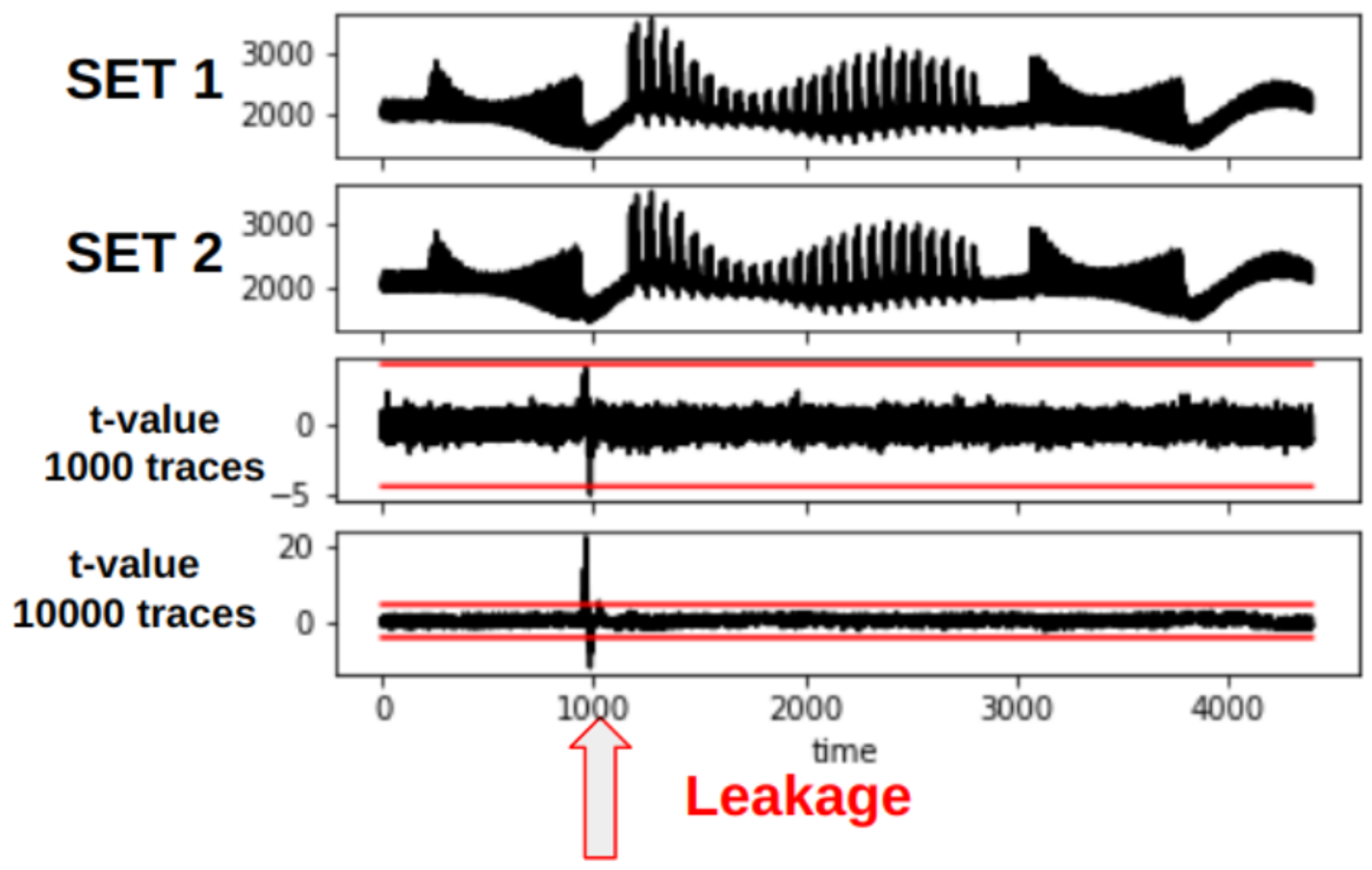 :--
Figure: TVLA plot showing leakage at around sample 1000. When increasing the number of traces (from 1000 to 10000), the leakage becomes more present. Note that the traces shown in this plot are taken from an arbitrary cryptographic hardware block and not AES.
:--
Figure: TVLA plot showing leakage at around sample 1000. When increasing the number of traces (from 1000 to 10000), the leakage becomes more present. Note that the traces shown in this plot are taken from an arbitrary cryptographic hardware block and not AES.
The prior Figure shows a TVLA plot that will be used throughout this document. The red lines mark the ± t-test border.
Dataset Generation for FvsR IV & Key
In TVLA, two different trace data sets need to be recorded. As described in the whitepaper, we generate these two trace data sets by using a fixed and a random AES-GCM cipher input set, i.e., the fixed and the random set.
| Input | Fixed Set | Random Set |
|---|---|---|
| Key | STATIC | RANDOM |
| IV | STATIC | RANDOM |
| PTX | STATIC | STATIC |
| AAD | STATIC | STATIC |
As shown in the table above, for our experiment we use a static cipher input for the fixed set. For the random set, we use a PRNG to randomly generate the secrets, i.e., key and IV, for each encryption. The dataset is generated directly on the device in the pentest framework. For each trace, ot-sca stores information to which dataset the trace belongs to.
With TVLA, the idea is to check whether we are able to distinguish power traces from the fixed and the random set.
Dataset Generation for FvsR PTX & AAD
For the second experiment, we use a static IV and key and calculate a FvsR PTX and AAD set:
| Input | Fixed Set | Random Set |
|---|---|---|
| Key | STATIC | STATIC |
| IV | STATIC | STATIC |
| PTX | STATIC | RANDOM |
| AAD | STATIC | RANDOM |
Results – FvsR IV & Key
In the following, we discuss the analysis results for each GCM phase. We start with the results for the FvsR IV & Key datasets.
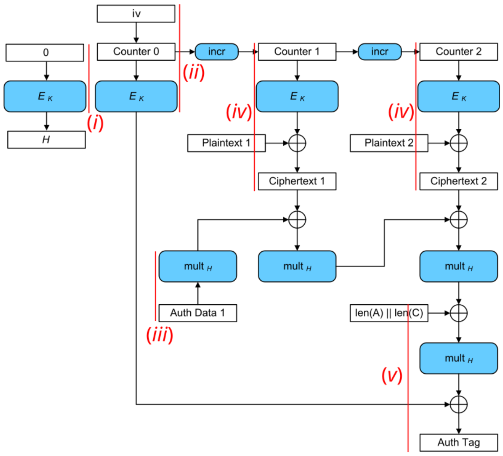 :--:
Figure: AES-GCM block diagram. Red lines mark the trigger windows for each analysis step.
:--:
Figure: AES-GCM block diagram. Red lines mark the trigger windows for each analysis step.
As shown in the prior Figure, we focus on analyzing (i) the generation of the hash subkey H, (ii) the encryption of the initial counter block S, (iii) the processing of the AAD blocks, (iv) the plaintext blocks, and (v) the tag generation. Each measurement is conducted with (a) masks off and (b) masks on to analyze the effectiveness of the masking countermeasure.
i) SCA Evaluation of Generating the Hash Subkey H
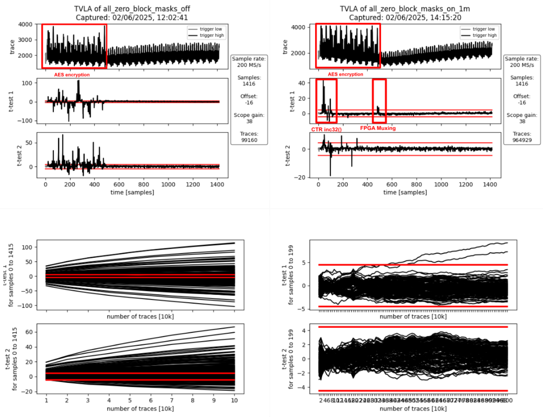 :--:
:--:
| Figure: Masking Off - 100k traces - Figure: Masking On - 1M traces |
Interpretation
The AES encryption is clearly visible in the form of 12 distinct peaks in the power traces shown in the prior set of Figures. The 12 peaks correspond to first the loading of the key and the all-zero block into the AES cipher core, followed by the initial round and the 10 full AES rounds (AES-128). They spread over approximately 470 samples which corresponds to the 56 target clock cycles a full AES-128 encryption takes.
If the masking is turned off (set of graphs), first and second-order leakage is clearly visible throughout the operation. If the masking is on (set of graphs), there is first-order leakage 1) at the beginning as well as 2) at the end of the operation.
- The leakage at the beginning of the operation is due to incrementing the IV/CTR value (inc32 function in GCM spec) which spreads across the first two AES rounds. This produces first-order leakage as the inc32 function implementation isn’t masked. It doesn’t need to be masked as the IV is not secret, just the encrypted initial counter block S (i.e., the encrypted IV) is secret in the context of GCM.
- The leakage at the end of the operation happens when the masked output of the AES cipher core, i.e., the masked hash subkey H, gets loaded in shares into the GHASH block. When studying the RTL, one can see that there is nothing in the path between the AES cipher core and the hash subkey registers inside the GHASH block that could combine the shares and cause this leakage. The leakage is most likely due to how the FPGA implementation tool maps the flip flops of the hash subkey register shares to the available FPGA logic slices: if flip flops of the different shares get mapped to the same logic slice, the carry-chain and other muxing logic present in the logic slice can combine the various inputs thereby causing SCA leakage despite these logic outputs not being used. We’ve observed similar effects in the past and there is research giving more insight into this and other FPGA-specific issues.
To summarize, the observed first-order leakage if masking is on is not of concern for ASIC implementations.
ii) SCA Evaluation of Encrypting the Initial Counter Block
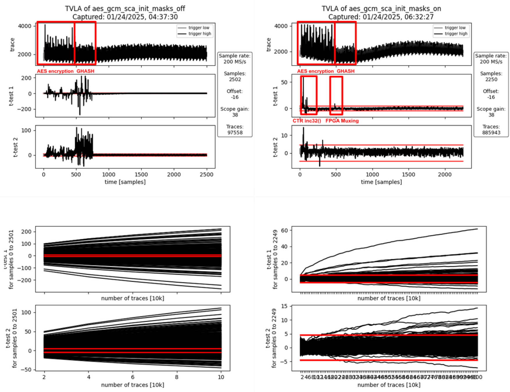 :--:
:--:
| Figure: Masking Off - 100k traces - Figure: Masking On - 1M traces |
Interpretation
Again, the AES encryption is clearly visible in the form of 12 peaks in the power traces shown in the prior set of Figures. This AES encryption corresponds to the generation of the encrypted initial counter block S. The AES encryption is followed by another operation visible in the power trace: the computation of repeatedly used correction terms using the Galois-field multipliers inside GHASH. This operation takes 33 target clock cycles (approximately 275 samples).
If the masking is turned off (set of graphs), first and second-order leakage is clearly visible throughout both operations while being more pronounced during the GHASH operation. This is because the GHASH block is smaller and thus produces less noise. If the masking is on (set of graphs), there is first-order leakage 1) at the beginning as well as 2) between the two operations.
- As before, the leakage at the beginning of the operation is due to incrementing the IV/CTR value (inc32 function in GCM spec) which spreads across the first two AES rounds. This produces first-order leakage as the inc32 function implementation isn’t masked. It doesn’t need to be masked as the IV is not secret, just the encrypted initial counter block S (i.e., the encrypted IV) is secret in the context of GCM.
- As before, the leakage at the end of the operation happens when the masked output of the AES cipher core, i.e., the encrypted initial counter block gets loaded in shares into the GHASH block. When studying the RTL, one can see that there is nothing in the path between the AES cipher core and the GHASH state registers inside the GHASH block that could combine the shares and cause this leakage. As before, the leakage is most likely due to how the FPGA implementation tool maps the multiplexers in front of the GHASH state registers to the available FPGA logic slices: Since the multiplexers for both shares use the same control signals, the multiplexing logic can be combined even into the same look-up tables (LUTs) thereby causing SCA leakage. We’ve observed similar effects in the past and there is research giving more insight into this and other FPGA-specific issues.
To summarize, the observed first-order leakage if masking is on is not of concern for ASIC implementations.
iii) SCA Evaluation of Processing the AAD Blocks
Processing AAD Block 0
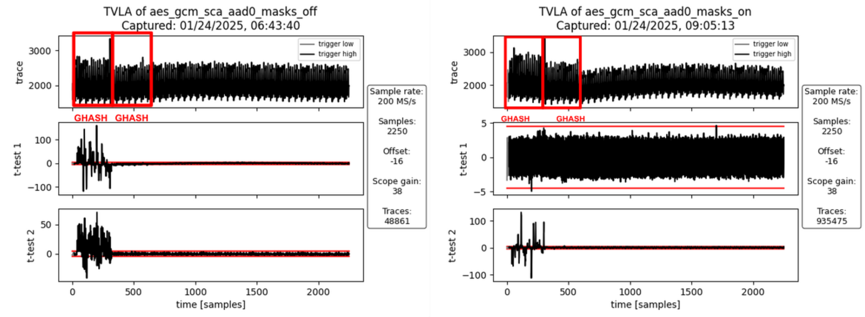 :--:
:--:
| Figure: Masking Off - 50k traces - Figure: Masking On - 10M traces |
Interpretation
For AAD blocks, the AES cipher core is not involved. However, during the computation of the first AAD block, the GHASH block needs to compute an additional correction term which is used for the very first block only. If the masking is turned off (first set of graphs), first- and second-order leakage is clearly visible but only for the first activity block. The second activity block involves computing the additional correction terms which requires Share 1 of the encrypted initial counter block to be multiplied by Share 1 of the hash subkey. But since the masking is off, both these values are zero for both the fixed and the random set and hence there is no SCA leakage. If the masking is turned on (second set of graphs), no SCA leakage is observable which is desirable.
Processing AAD Block 1
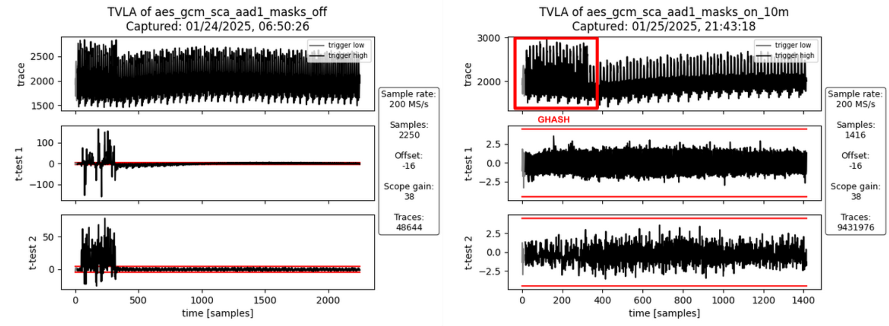 :--:
:--:
| Figure: Masking Off - 50k traces - Figure: Masking On - 10M traces |
Interpretation
For the second AAD block (and any subsequent AAD blocks) there is only one activity block corresponding to the Galois-field multiplication. If masking is turned off (first set of graphs), there is both first- and second-order leakage observable. If the masking is turned on (second set of graphs), no SCA leakage is observable which is desirable.
iv) SCA Evaluation of Processing the PTX Blocks
Processing PTX Block 0
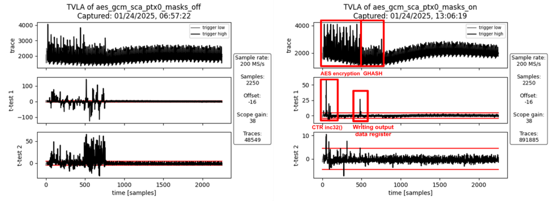 :--:
:--:
| Figure: Masking Off - 50k traces - Figure: Masking On - 1M traces |
Interpretation
Like in ii) SCA Evaluation of Encrypting the Initial Counter Block there is first-order leakage 1) at the beginning and 2) between the two operations if the masking is turned on (first set of graphs).
- As before, the leakage at the beginning of the operation is due to incrementing the IV/CTR value (inc32 function in GCM spec) which spreads across the first two AES rounds. This produces first-order leakage as the inc32 function implementation isn’t masked. It doesn’t need to be masked as the IV is not secret, just the encrypted initial counter block S (i.e., the encrypted IV) is secret in the context of GCM.
- The leakage between the two operations is due to the unmasking of the AES cipher core output, the addition of input data to produce the ciphertext, and writing this value to the GHASH block and the output data registers. It’s not related to the hash subkey H or the initial counter block S (i.e. the two secrets involved in the GHASH part of GCM). But since the AAD and the plaintext have been chosen to be the same for all traces in the fixed and the random sets, the traces of the fixed set only produce all the same ciphertext and thus are expected to exhibit a static power signature for this step, whereas the ciphertext of the random set is randomized through the random key and IV. However, since the ciphertext is not secret in the context of GCM, this leakage is of no concern.
To summarize, the observed first-order leakage if masking is on (second set of graphs) is not of concern.
Processing PTX Block 1
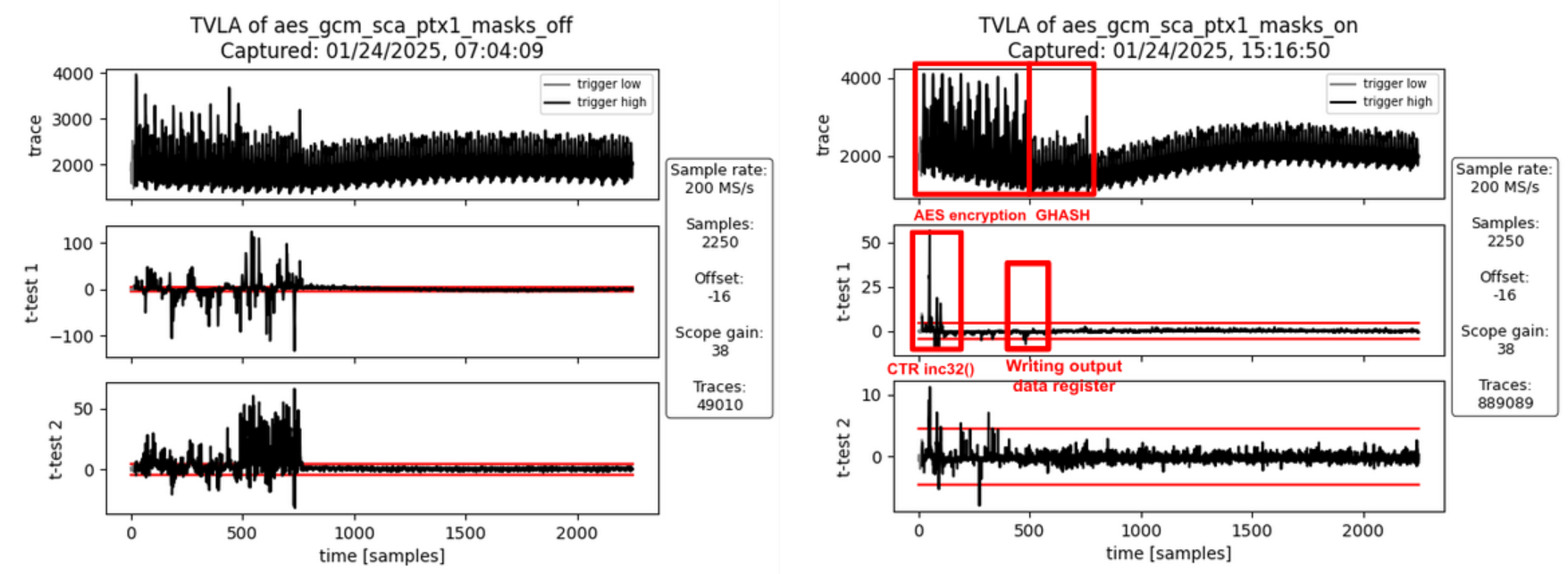 :--:
:--:
| Figure: Masking Off - 50k traces - Figure: Masking On - 1M traces |
Interpretation
As before (PTX Block 0), there is some first-order leakage observable when the masking is turned on. For the same reasons as before, this leakage is not of concern.
v) SCA Evaluation of the Tag Generation
 :--:
:--:
| Figure: Masking Off - 50k traces - Figure: Masking On - 1M traces |
Interpretation
The generation of the final authentication tag consists of two operations.
- The 128-bit block containing the AAD and ciphertext lengths is hashed and the correction terms are added. The GHASH state is unmasked (still masked with the encrypted initial counter block S) and Share 1 of S is added to write the final authentication tag to the data output registers readable by software.
- In parallel to writing the final authentication tag to the data output registers, the internal state is all cleared to random values and an additional multiplication is triggered to clear the internal state of the Galois-field multipliers and the correction term registers.
If masking is turned off (first set of graphs), there is both first- and second-order leakage observable during the first activity block (tag generation) but not during the clearing operation. If the masking is turned on (second set of graphs), some SCA leakage is observable between the two operations, i.e., when the final authentication tag is written to the output data registers. This leakage is expected as both the fixed and the random data sets use a static AAD and plaintext. This means, the tag for the fixed data set is fixed whereas the tags for the random set get randomized through the ciphertext (random due to the random key and IV).
To summarize, the observed first-order leakage if masking is on (second set of graphs) is not of concern.
Results – FvsR PTX & AAD
In the following, we discuss the analysis results for each FvsR PTX & AAD datasets. These experiments were specifically done to investigate leakage peaks identified for the FvsR Key & IV datasets that are attributed to how the FPGA implementation tool maps flip flops and multiplexer shares to the available FPGA logic slices.
i) SCA Evaluation of Generating the Hash Subkey H
 :--:
:--:
| Figure: Masking Off - 50k traces - Figure: Masking On - 1M traces |
Interpretation
There is no SCA leakage visible in both cases without masking (first set of graphs) and with masking turned on (second set of graphs). This is expected as the hash subkey generation doesn’t involve the plaintext and the AAD but only the key and IV. Both the fixed and random set use the same static key and IV.
This experiment was specifically done to check whether the leakage identified in i) SCA Evaluation of Generating the Hash Subkey H and attributed to how the FPGA implementation tool maps the flip flops of the hash subkey register shares to the available FPGA logic slices. As expected, the leakage peak is now gone.
ii) SCA Evaluation of Encrypting the Initial Counter Block
 :--:
:--:
| Figure: Masking Off - 50k traces - Figure: Masking On - 1M traces |
Interpretation
There is no SCA leakage visible in both cases without masking (first set of graphs) and with masking turned on (second set of graphs). This is expected as the encryption of the initial counter block and the subsequent computation of repeatedly used correction terms doesn’t involve the plaintext and the AAD but only the key and IV. Both the fixed and random set use the same static key and IV.
This experiment was specifically done to check whether the leakage identified in ii) SCA Evaluation of Encrypting the Initial Counter Block and attributed to how the FPGA implementation tool maps the multiplexers in front of the GHASH state registers to the available FPGA logic slices. As expected, the leakage peak is now gone.
iv) SCA Evaluation of Processing the PTX Block 0
 :--:
:--:
| Figure: Masking Off - 100k traces - Figure: Masking On - 1M traces |
Interpretation
With the masking turned off (first set of graphs), there is first-order leakage 1) at the beginning of the operation and 2) throughout the entire GHASH operation.
- The leakage at the beginning of the operation is due to the input data (the plaintext) being written to an internal buffer register. The AES cipher is operated in counter mode, meaning it doesn’t encrypt the input data but the counter value (incremented IV). Because the IV is fixed for both the fixed and the random data set, no leakage is observed during the AES encryption even if the masking is off. At the end of the AES encryption, the output of the AES cipher core is added to the content of the buffer register to produce the ciphertext which is then forwarded to the GHASH block and to the data output registers.
- The GHASH operation then processes this ciphertext. The observed leakage when the masking is off is expected.
With the masking turned on (second set of graphs), the first-order leakage at the beginning of the operation remains visible. The reason for this is that the internal register buffering the previous input data is not masked. This is of no concern as the leakage is not related to key or IV.
Another first-order leakage peak is visible between the AES encryption and the GHASH operation. This leakage is due to the unmasked AES cipher core output being added to the input data (coming from the internal buffer register) and the result being stored to the output data register. As key and IV are static and identical for both the fixed and the random data set, the cipher core output is the same for both sets. Any difference in the power signature between the two sets is due to the different plaintext / ciphertext. Again, this is to be expected and of no concern as the ciphertext is not secret in the context of GCM.
Reproducing the FPGA Experiments
Prerequisites
(i) Setting up the CW310 and CW Husky
Please follow the guide here to prepare the CW310 and CW Husky for the SCA measurements.
(ii) Generating the FPGA Bitstream
Follow the guide here to install Xilinx Vivado. Please note that a valid license is needed to generate bitstreams for the CW310 FPGA board.
Then, build the bitstream from the aes-gcm-sca-bitstream branch. This branch includes the AES-GCM and applies several optimizations (disabling certain features to reduce the area utilization) to improve the SCA measurements.
git clone https://github.com/vogelpi/opentitan.git
cd opentitan
git checkout aes-gcm-sca-bitstream
./bazelisk.sh build //hw/bitstream/vivado:fpga_cw310_test_rom
cp bazel-bin/hw/bitstream/vivado/build.fpga_cw310/synth-vivado/lowrisc_systems_chip_earlgrey_cw310_0.1.bit .
The resulting bitstream is lowrisc_systems_chip_earlgrey_cw310_0.1.bit.
(iii) Compiling the Penetration Testing Binary
The penetration testing binary that is running on the target is the framework that receives commands from the side-channel evaluation framework and triggers the AES-GCM operations.
git clone <https://github.com/vogelpi/opentitan.git>
cd opentitan
git checkout aes-gcm-review
./bazelisk.sh build //sw/device/tests/penetrationtests/firmware:firmware_fpga_cw310_test_rom
cp bazel-bin/sw/device/tests/penetrationtests/firmware/firmware_fpga_cw310_test_rom_fpga_cw310_test_rom.bin sca_ujson_fpga_cw310.bin
The resulting penetration testing binary is sca_ujson_fpga_cw310.bin.
(iv) Setting up the Side-Channel Evaluation Framework
Clone the ot-sca repository and switch to the dedicated AES-GCM branch:
git clone <https://github.com/lowRISC/ot-sca.git>
cd ot-sca
git checkout ot-sca-aes-gcm
Then, follow this guideline to prepare your machine for the measurements.
Afterwards, copy the bitstream to ot-sca/objs/lowrisc_systems_chip_earlgrey_cw310_0.1.bit and the binary to ot-sca/objs/sca_ujson_fpga_cw310.bin.
Finally, determine the port the CW310 opened on your machine (e.g., /dev/ttyACM2) and set it accordingly in the port field of the ot-sca/capture/configs/aes_gcm_sca_cw310.yaml configuration file.
Capturing Traces
After fulfilling the prerequisites, traces can be captured using ot-sca.
To configure the measurement, adapt the script located in ot-sca/capture/configs/aes_gcm_sca_cw310.yaml.
The following parameters can be changed:
husky:
  # Number of encryptions performed in one batch.
  num_segments: 35
  # Number of cycles that are captured by the CW Husky.
  num_cycles: 320
capture:
  # Number of traces to capture.
  num_traces: 100000
  # Number of traces to keep in memory before flushing to the disk.
  trace_threshold: 50000
test:
  # Values used for the fixed set.
  iv_fixed: [0xDE, 0xAD, 0xBE, 0xEF, 0xCA, 0xFE, 0xBA, 0xAD, 0xF0, 0xCA,
             0xCC, 0x1A, 0x00, 0x00, 0x00, 0x00]
  key_fixed: [0x81, 0x1E, 0x37, 0x31, 0xB0, 0x12, 0x0A, 0x78, 0x42, 0x78,
              0x1E, 0x22, 0xB2, 0x5C, 0xDD, 0xF9]
  # Static values that are used by the fixed and the random set.
  ptx_blocks: 2
  ptx_static: [[0xAA, 0xAA, 0xAA, 0xAA, 0xAA, 0xAA, 0xAA, 0xAA, 0xAA, 0xAA,
                0xAA, 0xAA, 0xAA, 0xAA, 0xAA, 0xAA], [0xBB, 0xBB, 0xBB,
                0xBB, 0xBB, 0xBB, 0xBB, 0xBB, 0xBB, 0xBB, 0xBB, 0xBB, 0xBB,
                0xBB, 0xBB, 0xBB]]
  ptx_last_block_len_bytes: 16
  aad_blocks: 2
  aad_static: [[0xCC, 0xCC, 0xCC, 0xCC, 0xCC, 0xCC, 0xCC, 0xCC, 0xCC, 0xCC,
                 0xCC, 0xCC, 0xCC, 0xCC, 0xCC, 0xCC], [0xDD, 0xDD, 0xDD,
                 0xDD, 0xDD, 0xDD, 0xDD, 0xDD, 0xDD, 0xDD, 0xDD, 0xDD,
                 0xDD, 0xDD, 0xDD, 0xDD]]
  aad_last_block_len_bytes: 16
  # Trigger configuration (select only one).
  # [Hash sub key, Init. block, AAD block, PTX block, TAG block]
  triggers: [False, False, False, False, True]
  # Which AAD or PTX block.  0 = first block.
  trigger_block: 0
  # 32-bit seed for masking on device. To switch off the masking, use 0
  # as an LFSR seed.
  lfsr_seed: 0x00000000
  #lfsr_seed: 0xdeadbeef
After tweaking the configuration, the traces can be captured by executing:
cd capture
./capture_aes_gcm.py -c configs/aes_gcm_sca_cw310.yaml -p aes_gcm_sca
Where the -c parameter is the config and -p the database where the traces are stored.
Performing the TVLA
After capturing the traces, the TVLA can be performed by switching into the ot-sca/analysis folder, copying the ot-sca/analysis/configs/tvla_cfg_kmac.yaml file to ot-sca/analysis/configs/tvla_cfg_aes_gcm.yaml, and modifying the configuration file:
project_file: ../capture/projects/aes_gcm_sca
trace_file: null
trace_start: null
trace_end: null
leakage_file: null
save_to_disk: null
save_to_disk_ttest: null
round_select: null
byte_select: null
input_histogram_file: null
output_histogram_file: null
number_of_steps: 1
ttest_step_file: null
plot_figures: true
test_type: "GENERAL_KEY"
mode: aes
filter_traces: true
trace_threshold: 50000
trace_db: ot_trace_library
By calling
./tvla.py --cfg-file tvla_cfg_aes_gcm.yaml run-tvla
the TVLA plot is generated.
PCR vault
- Platform Configuration Register (PCR) vault is a register file that stores measurements to be used by the microcontroller.
- PCR entries are read-only registers of 512 bits each.
- Control bits allow for entries to be cleared by FW, which sets their values back to 0.
- A lock bit can be set by FW to prevent the entry from being cleared. The lock bit is sticky and only resets on a powergood cycle.
| PCRV register | Address Offset | Description |
|---|---|---|
| PCR Control[31:0] | 0x1001a000 | 32 Control registers, 32 bits each |
| PCR Entry[31:0][11:0][31:0] | 0x1001a600 | 32 PCR entries, 384 bits each |
PCR vault functional block
PCR entries are hash extended using a hash extension function. The hash extension function takes the data currently in the PCR entry specified, concatenates data provided by the FW, and performs a SHA384 function on that data, storing the result back into the same PCR entry.
PCR hash extend function
FW provides the PCR entry to use as source and destination of the hash extend. HW copies the PCR into the start of the SHA block and locks those dwords from FW access. FW then provides the new data, and runs the SHA function as usual. After initialization, the locked dwords are unlocked.
FW must set a last cycle flag before running the last iteration of the SHA engine. This could be the first “init” cycle, or the Nth “next” cycle. This flag allows HW to copy the final resulting hash output back to the source PCR.
PCR signing
- PCR signing uses the key in key slot index 7 for PCR signing
- HW implements a HW function called GEN_PCR_HASH
- HW reads all the PCRs from all the PCR slots and hash extends them along with the NONCE that Caliptra FW provides
- PCR Hash = Hash(PCR[0], …, PCR[31], Nonce)
- HW also implements a HW function called SIGN_PCR. This function takes the PCR digest that was generated by the previous routine and signs it using the key in key slot 7, following the same ECC sign flow defined in the ECC section.
- The resulting PCR DIGEST is used only once for signing by the HW. If a new PCR signing is required, GEN_PCR_HASH needs to be redone.
ICCM write hash measurement (PCR4/PCR5)
The SHA-512 accelerator (sha512_acc_top) includes an ICCM hash mode that provides hardware-only measurement of all data written to ICCM during firmware loading. This creates a tamper-evident record of what code actually landed in instruction memory, closing the gap between "firmware image was verified" and "firmware image was correctly copied."
Overview
Two dedicated PCR entries are used:
| PCR | Name | Reset | Behavior |
|---|---|---|---|
| PCR4 | ICCM Current | Cleared on fw_update_reset (iccm_unlock) | Extended from zero on each firmware load — reflects only the currently running image |
| PCR5 | ICCM Journey | Cleared only on cold reset (cptra_pwrgood) | Extended from previous value on each firmware load — accumulates a chain of all images ever loaded |
Both PCR entries are write-protected: only the ICCM hash engine (pv_write[1]) can write nonzero values to PCR4 and PCR5. The normal SHA512/crypto PCR extend path (pv_write[0]) and firmware AHB writes are blocked from targeting these entries. Firmware may clear PCR4 or PCR5 to zero via PCR_CTRL[n].clear as a field escape hatch, but cannot write arbitrary values.
Operation
-
Autonomous arming: HW measures the ICCM region automatically. The existing per-bank ICCM-write snoop sets a sticky internal
iccm_armedflag on the very first write it sees after reset (or afterfw_update_resetreleases theiccm_unlock-driven clear). On the same cycle, HW acquires the SHA accelerator lock via the LOCK register'shwsetpath, blocking any concurrent SOC access for the duration of the measurement. Firmware does not need to take any action to enable the feature; ROM simply performs the memcpy as normal. -
ICCM write capture: As ROM copies firmware from the mailbox to ICCM via CPU store instructions, each ICCM bank write is captured by the SHA accelerator and accumulated into a SHA-384 hash. The hash runs in parallel with the copy — no backpressure or stall. Data is hashed as little-endian 32-bit words (native CPU byte order). The combinational OR of the live snoop into the
iccm_modeenable guarantees the very first dword is captured in the same cycle, beforeiccm_armeditself updates on the next clock edge. -
Finalization on ICCM lock: When ROM sets
INTERNAL_ICCM_LOCK, the SHA accelerator finalizes the hash (padding and last compression), producing a 384-bit ICCM digest. -
PCR extend: An internal FSM then performs proper PCR extend operations:
- Reads PCR4 current value (zeros after clear), computes
SHA-384(PCR4 || ICCM_digest), writes result to PCR4 - Reads PCR5 current value, computes
SHA-384(PCR5 || ICCM_digest), writes result to PCR5 - The extend uses the same
sha512_coreinstance with the same byte ordering as the normal PCR hash extend path, ensuring consistent results
- Reads PCR4 current value (zeros after clear), computes
-
Lock release: After both PCR extends complete, the sticky
iccm_mode_doneflag latches (blocking re-trigger until the nexticcm_unlock) and the SHA accelerator lock is released for normal firmware use.
Security properties
- HW-autonomous arming closes the bypass window where firmware could "forget" to enable the feature — the hash starts unconditionally on the first ICCM write the snoop sees
- ICCM measurement is single-shot per boot cycle: once
iccm_mode_donelatches, firmware cannot re-trigger it to overwrite PCR4/PCR5 - The hash captures the ground truth of ICCM write data at the memory bank interface — eliminating TOCTOU gaps between verification and copy
- Skipping any step (trigger, copy, or lock) results in empty PCRs, causing attestation failure
- The feature operates correctly regardless of
boot_flow_monitor_en— if debug-unlocked tests skip ICCM mode, PCRs stay empty and attestation fails (no security bypass) - PCR4 clear mechanism (
pcr4_hwclr) is tied toiccm_unlock(fires onfw_update_reset), ensuring fresh measurement on each firmware update
Timing impact
The SHA-384 computation runs in parallel with ROM's ICCM copy. Only finalization (~80 cycles) and the two PCR extend operations (~210 cycles total) occur after ICCM_LOCK is set. Total added latency: ~290 cycles, invisible to boot time.
Key vault
Key Vault (KV) is a register file that stores the keys to be used by the microcontroller, but this register file is not observed by the microcontroller. Each cryptographic function has a control register and functional block designed to read from and write to the KV.
| KV register | Description |
|---|---|
| Key Control[23:0] | 24 Control registers, 32 bits each |
| Key Entry[23:0][15:0][31:0] | 24 Key entries, 512 bits each No read or write access |
Key vault functional block
Keys and measurements are stored in 512b register files. These have no read or write path from the microcontroller. The entries are read through a passive read mux driven by each cryptographic block. Locked entries return zeroes.
Entries in the KV must be cleared via control register, or by de-assertion of pwrgood.
Each entry has a control register that is writable by the microcontroller.
The destination valid field is programmed by FW in the cryptographic block generating the key, and it is passed here at generation time. This field cannot be modified after the key is generated and stored in the KV.
| KV Entry Ctrl Fields | Reset | Description |
|---|---|---|
| Lock wr[0] | core_only_rst_b | Setting the lock wr field prevents the entry from being written by the microcontroller. Keys are always locked. After a lock is set, it cannot be reset until cptra_rst_b is de-asserted. |
| Lock use[1] | core_only_rst_b | Setting the lock use field prevents the entry from being used in any cryptographic blocks. After the lock is set, it cannot be reset until cptra_rst_b is de-asserted. |
| Clear[2] | cptra_rst_b | If unlocked, setting the clear bit causes KV to clear the associated entry. The clear bit is reset after entry is cleared. |
| rsvd0[3] | ||
| rsvd1[8:4] | ||
| Dest_valid[16:9] | hard_reset_b | KV entry can be used with the associated cryptographic block if the appropriate index is set. [0] - HMAC KEY [1] - HMAC BLOCK [2] - MLDSA SEED [3] - ECC PRIVKEY [4] - ECC SEED [5] - AES KEY [6] - MLKEM SEED [7] - MLKEM MSG [8] - AXI DMA DATA |
| last_dword[20:19] | hard_reset_b | Store the offset of the last valid dword, used to indicate the last cycle for read operations. |
Key vault cryptographic functional block
A generic block is instantiated in each cryptographic block to enable access to KV.
Each input to a cryptographic engine can have a key vault read block associated with it. The KV read block takes in a key vault read control register that drives an FSM to copy an entry from the key vault into the appropriate input register of the cryptographic engine.
Each output generated by a cryptographic engine can have its result copied to a slot in the key vault. The KV write block takes in a key vault write control register. This register drives an FSM to copy the result from the cryptographic engine into the appropriate key vault entry. It also programs a control field for that entry to indicate where that entry can be used.
After programming the key vault read control, FW needs to query the associated key vault read status to confirm that the requested key was copied successfully. After valid is set and the error field reports success, the key is ready to be used.
Similarly, after programming the key vault write control and initiating the cryptographic function that generates the key to be written, FW needs to query the associated key vault write status to confirm that the requested key was generated and written successfully.
While the crypto engine, key vault read, or key vault write blocks are active, the read and write control registers are locked. After reading the status register and confirming that the operation was successful, the next key vault control can be programmed.
When a key is read from the key vault, the API register is locked and any result generated from the cryptographic block is not readable by firmware. The digest can only be sent to the key vault by appropriately programming the key vault write controls. After the cryptographic block completes its operation, the lock is cleared and the key is cleared from the API registers.
Key vault read errors will prevent the crypto engine from accepting new commands. The engine will require zeroization in order to clear the error and resume normal operation.
If multiple iterations of the cryptographic function are required, the key vault read and write controls must be programmed for each iteration. This ensures that the lock is set and the digest is not readable.
The following tables describe read, write, and status values for key vault blocks.
| KV Read Ctrl Reg | Description |
|---|---|
| read_en[0] | Indicates that the read data is to come from the key vault. Setting this bit to 1 initiates copying of data from the key vault. |
| read_entry[5:1] | Key vault entry to retrieve the read data from the engine. |
| pcr_hash_extend[6] | Requested entry is a PCR. This is used only for the SHA engine to hash extend. It is not functional in any other cryptographic engine. |
| rsvd[31:7] | Reserved field |
| KV Write Ctrl Reg | Description |
|---|---|
| write_en[0] | Indicates that the result is to be stored in the key vault. Setting this bit to 1 copies the result to the key vault when it is ready. |
| write_entry[5:1] | Key vault entry to store the result. |
| hmac_key_dest_valid[6] | HMAC KEY is a valid destination. |
| hmac_block_dest_valid[7] | HMAC BLOCK is a valid destination. |
| mldsa_seed_dest_valid[8] | MLDSA SEED is a valid destination. |
| ecc_pkey_dest_valid[9] | ECC PKEY is a valid destination. |
| ecc_seed_dest_valid[10] | ECC SEED is a valid destination. |
| aes_key_dest_valid[11] | AES KEY is a valid destination. |
| mlkem_seed_dest_valid[12] | MLKEM SEED is a valid destination. |
| mlkem_msg_dest_valid[13] | MLKEM MSG is a valid destination. |
| dma_data_dest_valid[14] | DMA DATA is a valid destination. |
| rsvd[31:15] | Reserved field |
| KV Status Reg | Description |
|---|---|
| ready[0] | Key vault control is idle and ready for a command. |
| valid[1] | Requested flow is done. |
| error[9:2] | SUCCESS - 0x0 - Key Vault flow was successful KV_READ_FAIL - 0x1 - Key Vault Read flow failed KV_WRITE_FAIL - 0x2 - Key Vault Write flow failed |
Key vault endianness and byte ordering
The Key Vault stores each entry as an array of 16 DWORDs (32-bit words), indexed KV[0] through KV[15]. The KV read and write clients perform byte and DWORD ordering transformations so that data written by one engine can be correctly consumed by another.
The KV write client has a configurable parameter, KV_WRITE_SWAP_DWORDS, that controls DWORD ordering when writing result data into a KV entry. When set to 1 (default), the write client reverses DWORD order so that KV[0] holds the most-significant DWORD: KV[offset] = data[N−1−offset]. When set to 0, DWORDs are stored sequentially: KV[offset] = data[offset]. The KV read client always reads sequentially from KV[0] through KV[15]; each engine applies its own register-level mapping.
Per-engine endianness conventions
| Engine | Native endianness | KV write SWAP_DWORDS | KV read register mapping | Notes |
|---|---|---|---|---|
| HMAC-512 | Big-endian | 1 (default) | Sequential: BLOCK[d] = KV[d], KEY[d] = KV[d] | Block read supports PAD and HMAC auto-padding. |
| SHA-512 | Big-endian | 1 (default) | Sequential: BLOCK[d] = KV[d] | Block read supports PAD. |
| ECC (P-384) | Big-endian | 1 (default) | Sequential: PRIVKEY[d] = KV[d], SEED[d] = KV[d] | -- |
| AES | Little-endian | 0 | Byte swap per DWORD: key_reg[d][b] = KV_data[3−b] | CTRL0.ENDIAN_SWAP optionally swaps bytes in FW DATA_IN/DATA_OUT registers. |
| ML-KEM | Little-endian | 0 | DWORD-reversed: SEED_D[d] = KV[N−1−d], SEED_Z[i] = KV[2N−1−i] | Shared key undergoes DWORD reversal in the ABR controller before the write client. |
| ML-DSA | Little-endian | N/A (no KV write) | DWORD-reversed: SEED[d] = KV[N−1−d] | -- |
Write path: HMAC, SHA-512, and ECC produce results with the most-significant DWORD at the highest internal index; the write client reversal (SWAP_DWORDS=1) places the most-significant DWORD at KV[0]. AES stores its 128-bit (4 DWORD) output sequentially. The ML-KEM shared key is pre-reversed in the ABR controller (mlkem_sharedkey_data[d] = shared_key[SHAREDKEY_NUM_DWORDS-1-d]), producing the same KV layout as the big-endian engines despite using SWAP_DWORDS=0.
Read path: Big-endian engines (HMAC, SHA-512, ECC) use sequential mapping; register[d] receives KV[d]. AES applies a per-DWORD byte swap to convert from big-endian to its little-endian internal format. ML-KEM and ML-DSA reverse the DWORD index (SEED[d] is written when kv_read_offset == N-1-d), producing a full byte reversal of the original data.
Firmware byte-ordering rules
When firmware passes data between engines via software registers (without using KV), it must perform the following transformations. In this table, "big-endian" means the lowest-addressed register (index 0) holds the most-significant DWORD; "little-endian" means index 0 holds the least-significant DWORD. AES is little-endian but additionally byte-swaps each DWORD on the KV read path, so firmware must apply BSWAP32 per DWORD when writing AES key registers directly.
| Source → Destination | Transformation | Example |
|---|---|---|
| Big-endian → big-endian | Copy DWORDs directly | HMAC tag → ECC seed |
| Big-endian → little-endian | Reverse DWORD order: DEST[i] = SRC[N−1−i] | HMAC tag → ML-KEM seed |
| Big-endian → AES | Byte-swap each DWORD: AES_KEY[i] = BSWAP32(src[i]) | HMAC tag → AES key |
| Little-endian → AES | Reverse DWORDs and byte-swap each: AES_KEY[i] = BSWAP32(src[N−1−i]) | ML-KEM shared key → AES key |
| Little-endian → big-endian (non-AES) | Reverse DWORD order only: DEST[i] = src[N−1−i] | ML-KEM shared key → HMAC block |
De-obfuscation engine
To protect software intellectual property from different attacks and, particularly, for thwarting an array of supply chain threats, code obfuscation is employed. Hence, the de-obfuscation engine is implemented to decrypt the code.
Advanced Encryption Standard (AES) is used as a de-obfuscation function to encrypt and decrypt data [4]. The hardware implementation is based on Secworks/aes [1]. The implementation supports the two variants: 128- and 256-bit keys with a block/chunk size of 128 bits.
The AES algorithm is described as follows:
- The key is fed to an AES core to compute and initialize the round key
- The message is broken into 128-bit chunks by the host
- For each chunk:
- The message is fed to the AES core
- The AES core and its working mode (enc/dec) are triggered by the host
- The AES core status is changed to ready after encryption or decryption processing
- The result digest can be read before processing the next message chunks
Key vault de-obfuscation block operation
A de-obfuscation engine (DOE) is used in conjunction with AES cryptography to de-obfuscate the UDS and field entropy and HEK seed.
- The obfuscation key is wired to DOE engine. The data to be decrypted (either obfuscated UDS, obfuscated field entropy, or obfuscated HEK seed) is fed into the DOE data.
- An FSM manually drives the DOE engine and writes the decrypted data back to the key vault.
- FW programs the DOE with the requested function (UDS, field entropy, or HEK seed de-obfuscation), and the destination for the result.
- After de-obfuscation is complete, FW can clear out the UDS, field entropy, and HEK seed values from any flops until cptra_pwrgood de-assertion.
The following tables describe DOE register and control fields.
| DOE Register | Address | Description |
|---|---|---|
| IV | 0x10000000 | 128 bit IV for DOE flow. Stored in big-endian representation. |
| CTRL | 0x10000010 | Controls for DOE flows. |
| STATUS | 0x10000014 | Valid indicates the command is done and results are stored in key vault. Ready indicates the core is ready for another command. |
| DOE Ctrl Fields | Reset | Description |
|---|---|---|
| CMD[1:0] | Cptra_rst_b | 2’b00 Idle 2’b01 Run UDS flow 2’b10 Run FE flow 2’b11 Clear Obf Secrets |
| DEST[6:2] | Cptra_rst_b | Destination register for the result of the de-obfuscation flow. Field entropy writes into DEST and DEST+1 Key entry only, can’t go to PCR . |
| CMD_EXT[8:7] | Cptra_rst_b | 2’b00 Idle (or running a standard, non-extended command) 2’b01 Run OCP LOCK HEK seed flow 2’b10 RESERVED 2’b11 RESERVED |
Key vault de-obfuscation flow
- ROM loads IV into DOE. ROM writes to the DOE control register the destination for the de-obfuscated result and sets the appropriate bit to run UDS, field entropy, and/or HEK seed flow.
- DOE state machine takes over and loads the Caliptra obfuscation key into the key register.
- Next, either the obfuscated UDS or field entropy are loaded into the block register 4 DWORDS at a time.
- Results are written to the KV entry specified in the DEST field of the DOE control register.
- State machine resets the appropriate RUN bit when the de-obfuscated key is written to KV. FW can poll this register to know when the flow is complete.
- The clear obf secrets command flushes the obfuscation key, the obfuscated UDS, and the field entropy from the internal flops. This should be done by ROM after both de-obfuscation flows are complete.
Key vault boot flow transition enforcement
The Key Vault Boot Flow Transition Enforcement feature provides hardware-enforced integrity monitoring and access control for DICE key derivation across boot phase transitions (ROM->FMC->RT). It detects ICCM code execution transitions, validates key vault state at each boundary, and atomically applies lock/clear enforcement to key slots.
Overview
The feature consists of three cooperating blocks:
- Boot Flow Monitor (in
caliptra_top): Detects ROM->FMC and FMC->RT transitions by observing ICCM memory bank read enables against programmed address regions. - KV Monitor (in
kv): Validates dest_valid permissions and crypto write counts on DICE key slots at each transition boundary. - KV Enforcement (in
kv): Atomically applies lock_wr, lock_use, and slot clearing at each transition.
Figure: KV Boot Flow Transition Enforcement high-level block diagram
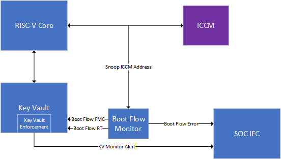
Boot flow monitor
The boot flow monitor detects firmware execution phase transitions by spying the ICCM memory interface. It compares bank-level read addresses against programmed FMC and RT region boundaries.
ICCM region registers
Four shadow-hardened registers define the FMC and RT code regions within ICCM address space:
| Register | Address | Description |
|---|---|---|
| INTERNAL_ICCM_FMC_START_ADDR | 0x30030650 | Start address of FMC region (18-bit ICCM-relative) |
| INTERNAL_ICCM_FMC_END_ADDR | 0x30030654 | End address of FMC region (inclusive) |
| INTERNAL_ICCM_RT_START_ADDR | 0x30030658 | Start address of RT region (18-bit ICCM-relative) |
| INTERNAL_ICCM_RT_END_ADDR | 0x3003065C | End address of RT region (inclusive) |
| INTERNAL_ICCM_REGION_LOCK | 0x30030660 | W1S lock -- once set, address registers cannot be modified until reset |
These registers use the caliptra_prim_subreg_shadow primitive for glitch hardening:
- 2-phase write protocol: Each register must be written twice with the same value to commit. A single write updates only the shadow copy; the second matching write commits to the primary register.
- Phase-clear-on-read: A read operation resets the write phase to 0, preventing stale partial writes from persisting.
- Error lockout: If the shadow and committed copies diverge (storage fault), all further writes are blocked until reset.
- Error reporting: Storage faults assert
CPTRA_HW_ERROR_FATAL.shadow_storage_err[5]. Phase-1/phase-0 mismatches assertCPTRA_HW_ERROR_NON_FATAL.shadow_update_err[3].
The effective lock for the boot flow monitor is iccm_region_lock & iccm_all_shadows_committed -- both the lock register must be set AND all four address registers must have completed their 2-phase writes.
Transition detection
The monitor uses MuBi4-encoded signals for glitch resistance:
| Signal | Encoding | Meaning |
|---|---|---|
boot_flow_fmc | MuBi4True/False | CPU has begun executing from the FMC region |
boot_flow_rt | MuBi4True/False | CPU has begun executing from the RT region |
boot_flow_error | MuBi4True/False | Fatal error detected in boot flow |
Transitions are one-way: once boot_flow_fmc becomes True, it remains True until reset. The monitor fires on the first ICCM read within the FMC region (after effective lock is set), and similarly for RT.
Error conditions
boot_flow_error is asserted (fatal) when any of the following occur:
- ICCM fetch while region lock is not set or shadow registers are not committed
- RT region fetch while
boot_flow_fmcis False (illegal ROM->RT jump -- the RT transition is gated on FMC, so this fires the error without producing a transientboot_flow_rtpulse) - ICCM fetch outside both the FMC and RT programmed regions after region lock is set (out-of-range execution)
- Any boot flow MuBi4 signal enters an invalid (non-True, non-False) encoding state
Simulation support
In simulation, boot_flow_monitor_en defaults to 0 (disabled). The testbench overrides this signal with a force when testing the feature. In hardware, the monitor is enabled when debug_locked is asserted AND scan_mode is deasserted. The monitor is disabled when debug is unlocked (to allow JTAG ICCM access and fake-ROM flows) and during scan mode (to prevent false transitions from clock-override activity on the ICCM banks).
KV monitor
At each boot phase transition, the KV monitor validates that the expected DICE key slots are correctly populated. The monitor checks only DICE derivation key slots (0–9) — optional feature keys (Stable Owner Key, OCP Lock keys) are excluded from monitoring because they are conditionally derived and do not participate in the DICE trust chain. A mismatch triggers kv_monitor_alert, which escalates to CPTRA_HW_ERROR_FATAL.kv_error[4] and flushes all key entries.
ROM->FMC checks (on enter_fmc)
| Slot | Name | Expected dest_valid |
|---|---|---|
| 0 | SI_IDEV | AES_KEY |
| 1 | SI_LDEV | AES_KEY |
| 2 | KEY_LADDER | HMAC_KEY |
| 6 | FMC_CDI | HMAC_KEY | MLDSA_SEED | ECC_SEED |
| 7 | FMC_ECDSA | ECC_PKEY |
| 8 | FMC_MLDSA | MLDSA_SEED |
Additionally, per-slot crypto write counters verify exact expected derivation counts:
- Slot 6 (FMC_CDI): == 4 writes (IDevID CDI + LDevID intermediate + LDevID CDI + FMC Alias CDI)
- Slot 7 (FMC_ECDSA): == 2 writes (IDevID ECC keygen + FMC Alias ECC keygen)
- Slot 8 (FMC_MLDSA): == 2 writes (IDevID MLDSA keygen + FMC Alias MLDSA keygen)
An exact match (rather than a minimum threshold) detects both truncated DICE chains (too few writes, indicating a skipped derivation step) and glitch-replayed operations (too many writes, which could overwrite the final safe key with an earlier intermediate value such as raw UDS).
Write counters are 3-bit saturating counters that reset only on hard reset (cptra_pwrgood) or flush_keyvault, persisting across warm and FW update resets. Since ROM does not re-derive DICE keys on warm or FW update reset, the counters retain their cold-boot values and pass the exact-match check on subsequent transitions.
FMC->RT checks (on enter_rt)
| Slot | Name | Expected dest_valid |
|---|---|---|
| 4 | RT_CDI | HMAC_KEY | MLDSA_SEED | ECC_SEED |
| 5 | RT_ECDSA | ECC_PKEY |
| 9 | RT_MLDSA | MLDSA_SEED |
KV enforcement
Enforcement is applied continuously based on the current boot phase and atomically at transitions.
Lock enforcement (continuous)
| Condition | Slots affected | Action |
|---|---|---|
boot_flow_fmc = True | 0, 1, 2, 6, 7, 8 | lock_wr asserted via hwset (HW-driven, cannot be cleared by SW) |
boot_flow_rt = True | 4, 5, 9 | lock_wr asserted via hwset |
boot_flow_rt = True | 6, 7, 8 | lock_use asserted via hwset (FMC keys cannot be used in RT) |
The lock_wr and lock_use fields have hwset property in the register definition, allowing hardware to set them without firmware intervention. Once set, they can only be cleared by core_only_rst_b de-assertion.
Slot clearing (atomic, on transition edge)
DICE slots — unconditionally cleared or preserved at each transition:
| Slot | Purpose | ROM→FMC | FMC→RT |
|---|---|---|---|
| 0 | SI_IDEV | Preserved | Preserved |
| 1 | SI_LDEV | Preserved | Preserved |
| 2 | KEY_LADDER | Preserved | Preserved |
| 3 | TMP | Cleared | Cleared |
| 4 | RT_CDI | Cleared | Preserved |
| 5 | RT_ECDSA | Cleared | Preserved |
| 6 | FMC_CDI | Preserved | Preserved |
| 7 | FMC_ECDSA | Preserved | Preserved |
| 8 | FMC_MLDSA | Preserved | Preserved |
| 9 | RT_MLDSA | Cleared | Preserved |
| 10–14 | Unused | Cleared | Cleared |
Conditionally-preserved slots — behavior depends on active mode:
| Slot | Purpose | Default (no optional features) | stable_owner_key_en | ocp_lock_mode_en |
|---|---|---|---|---|
| 15 | Stable Owner Key | Cleared | Preserved | Cleared (mutually exclusive) |
| 16 | MDK | Cleared | Cleared | Preserved |
| 17–21 | Unused OCP range | Cleared | Cleared | Cleared |
| 22 | HEK seed | Cleared | Cleared | Preserved |
| 23 | MEK | Cleared | Cleared | Always cleared (DMA-accessible) |
Clearing destroys the key data and resets dest_valid and last_dword for the affected slots.
Conditional slot preservation
Two optional Caliptra features populate KV slots that must survive boot transitions when the feature is active, but must be cleared when inactive. These slots are not monitored (no dest_valid checks, no write counters) — the monitor is exclusively for DICE keys. Only the enforcement block (slot clearing) handles them conditionally.
Stable Owner Key (Slot 15)
The Stable Owner Root Key is conditionally derived by ROM when all three conditions are met:
SUBSYSTEM_MODE_en= 1 (Caliptra operating in subsystem mode)OCP_LOCK_MODE_en= 0 (OCP Lock feature is not active)SS_STRAP_GENERIC[3][0]= 1 (SoC strap enabling the stable owner key feature)
The combined signal stable_owner_key_en is computed in soc_ifc_top and routed to the Key Vault. When active, slot 15 is excluded from boot_flow_key_clear at both ROM-to-FMC and FMC-to-RT transitions. When inactive, slot 15 is cleared normally.
OCP Lock Keys (Slots 16 and 22)
When OCP Lock mode is enabled (ocp_lock_mode_en = 1 from the ss_ocp_lock_en strap), DOE populates slot 16 (MDK) and slot 22 (HEK seed) before ROM runs. FMC and RT firmware require these keys for EPK, VEK, and MEK derivation in OCP Lock flows.
When ocp_lock_mode_en is active, slots 16 and 22 are excluded from clearing at both transitions. When inactive, they are cleared normally.
Slot 23 (MEK) is always cleared regardless of ocp_lock_mode_en. MEK has DMA_DATA in its dest_valid (it is DMA-accessible for key release), making it a security risk if it persists across transitions. RT firmware re-derives MEK when needed during OCP Lock key release flows.
Only the specific slots that ROM or FMC actually derive (16 and 22) are preserved — not the entire OCP Lock range (16–23). Slots 17–21 and 23 are always cleared.
Mutual exclusion: Stable Owner Key and OCP Lock are mutually exclusive by construction — stable_owner_key_en includes ~OCP_LOCK_MODE_en in its definition. When OCP Lock is enabled, slot 15 is always cleared even if SS_STRAP_GENERIC[3][0] = 1.
Error escalation
Any of the following trigger all key entries to be flushed:
boot_flow_error= MuBi4Truekv_monitor_alert(dest_valid mismatch or write count violation)kv_multi_write_err(existing: multiple crypto engines writing simultaneously)
The error is reported as CPTRA_HW_ERROR_FATAL.kv_error[4], which is unmasked and always triggers an interrupt.
DOE lockdown
Once the boot flow monitor detects that execution has transitioned to FMC or RT (i.e., boot_flow_fmc or boot_flow_rt is True), the DOE command register is forcibly cleared via doe_cmd_lock. This prevents any new de-obfuscation commands from being issued after the DICE key derivation phase is complete, closing the window for an attacker to re-derive secrets using the obfuscation key.
Error register summary
| Register | Bit | Field | Trigger |
|---|---|---|---|
| CPTRA_HW_ERROR_FATAL | 4 | kv_error | Boot flow error OR KV monitor alert |
| CPTRA_HW_ERROR_FATAL | 5 | shadow_storage_err | ICCM region shadow register storage fault |
| CPTRA_HW_ERROR_NON_FATAL | 3 | shadow_update_err | ICCM region shadow register phase mismatch |
DICE slot assignments
The following table documents the key vault slot assignments used by the DICE key derivation chain (defined in kv_defines_pkg.sv):
| Slot | Constant | Purpose |
|---|---|---|
| 0 | KV_SLOT_SI_IDEV | Silicon IDevID private key |
| 1 | KV_SLOT_SI_LDEV | Silicon LDevID private key |
| 2 | KV_SLOT_KEY_LADDER | Key ladder intermediate |
| 4 | KV_SLOT_RT_CDI | Runtime CDI |
| 5 | KV_SLOT_RT_ECDSA | Runtime ECDSA private key |
| 6 | KV_SLOT_FMC_CDI | FMC CDI (accumulates through DICE chain) |
| 7 | KV_SLOT_FMC_ECDSA | FMC ECDSA private key |
| 8 | KV_SLOT_FMC_MLDSA | FMC MLDSA private key |
| 9 | KV_SLOT_RT_MLDSA | Runtime MLDSA private key |
Conditionally-preserved slot assignments
The following slots are populated by optional features and conditionally preserved by enforcement (but not monitored):
| Slot | Constant | Feature | Preserved when |
|---|---|---|---|
| 15 | KV_SLOT_STABLE_OWNER | Stable Owner Root Key | stable_owner_key_en (subsystem mode, strap[3][0]=1, OCP Lock off) |
| 16 | OCP_LOCK_RT_OBF_KEY_KV_SLOT | MDK (runtime obfuscation key) | ocp_lock_mode_en |
| 22 | OCP_LOCK_HEK_SEED_KV_SLOT | HEK seed | ocp_lock_mode_en |
| 23 | OCP_LOCK_MEK_KV_SLOT | MEK (key release) | Never (always cleared — DMA-accessible, security risk) |
ROM programming sequence
ROM must perform the following steps before jumping to FMC:
- Complete all DICE key derivations (DOE decrypt, HMAC, ECC keygen, MLDSA keygen)
- Program ICCM region registers with 2-phase writes:
- Write
INTERNAL_ICCM_FMC_START_ADDRtwice with the same value - Write
INTERNAL_ICCM_FMC_END_ADDRtwice with the same value - Write
INTERNAL_ICCM_RT_START_ADDRtwice with the same value - Write
INTERNAL_ICCM_RT_END_ADDRtwice with the same value
- Write
- Set
INTERNAL_ICCM_REGION_LOCK(W1S) -- this arms the boot flow monitor - Jump to FMC entry point in ICCM
The first instruction fetch from the FMC region triggers the ROM->FMC transition, at which point the KV monitor validates slot state and enforcement atomically applies locks and clears.
Data vault
Data vault is a set of generic scratch pad registers with specific lock functionality and clearable on cold and warm resets.
- 48B scratchpad registers that are lockable but cleared on cold reset (10 registers)
- 48B scratchpad registers that are lockable but cleared on warm reset (10 registers)
- 4B scratchpad registers that are lockable but cleared on cold reset (8 registers)
- 4B scratchpad registers that are lockable but cleared on warm reset (10 registers)
- 4B scratchpad registers that are cleared on warm reset (8 registers)
OCP LOCK Hardware Architecture
Overview
The following hardware and ROM/FW enhancements support the OCP L.O.C.K. (a.k.a. OCP LOCK) flows defined for SSD applications. The specification is available here:
OCP LOCK Spec
Additional Registers, Straps, and Macros for OCP LOCK
-
SS_OCP_LOCK_CTRL.LOCK_IN_PROGRESS
A status/control bit used to enforce the new key Vvult (KV) rules required by OCP LOCK. Write-1-to-set, meaning that, once-enabled, OCP LOCK functionality will persist until the register is cleared by a cold reset. See the dedicated section below for details on the behaviors this register enables. -
ss_ocp_lock_en(constant-value input strap) with a corresponding bit inCPTRA_HW_CONFIGregister namedOCP_LOCK_MODE_en:- Enables Caliptra ROM to perform OCP LOCK operations (e.g., using DOE for HEK seed de-obfuscation, Key Release via AXI DMA).
- Allows the ROM to set
SS_OCP_LOCK_CTRL.LOCK_IN_PROGRESS. ss_ocp_lock_enis a strap pin and must be driven with a constant value by the integrator.CPTRA_HW_CONFIGregister samples this strap and store its value inOCP_LOCK_MODE_enbit- This bit is only reflected in CPTRA_HW_CONFIG if CALIPTRA_MODE_SUBSYSTEM is defined
-
HEK seed fuse register
Holds the obfuscated HEK seed. ROM is responsible for performing the operation to de-obfuscate the HEK seed. -
Key release address and size straps
Writable untilFUSE_WR_DONE, then locked (same as fuses and other subsystem-mode straps).- Address strap (
strap_ss_key_release_base_addr): full destination address for key release; in OCP LOCK this is the destination for the MEK to be written. Firmware can derive the SFR base from this value as needed. - Size strap (
strap_ss_key_release_key_size): byte-count (dword-aligned count is required by HW) of the key to program to the destination address via the key release operation. Strap input values are forced to a dword value by hardware. If control firmware updates this value (prior to FUSE_WR_DONE being set), it must use a dword-aligned value.
- Address strap (
Refer to the Caliptra Integration Spec for more details about macros and strap pins.
SS_OCP_LOCK_CTRL.LOCK_IN_PROGRESS Register Bit
When/How it is set
- Set by Caliptra ROM after performing OCP LOCK-related derivations (HEK, MDK, etc.).
- Can be set iff (
ss_ocp_lock_enis set to 1 ANDCALIPTRA_MODE_SUBSYSTEMis defined). - Once set, a value of 1 persists until the register is cleared by cold reset.
Enforcements/Effects
- Reserves key vault slots 0–15 for standard use-cases.
- Reserves key vault slots 16–23 for OCP LOCK use-cases.
- Key Vault slot 16 (KV16) is reserved for holding the MDK
- Key Vault slot 23 (KV23) is reserved for holding the MEK
- Blocks interactions between standard slots and LOCK slots. This means that any crypto operation that uses a Key Vault input value (e.g. for Key, Block, Seed inputs) may not write the output to a Key Vault from a different region. E.g., When
SS_OCP_LOCK_CTRL.LOCK_IN_PROGRESSis set, HMAC may not perform an operation that uses Key Vault slot 8 as BLOCK input and writes the output TAG to Key Vault slot 17. - Enables Key Release via AXI DMA.
- Enables AES engine to write output to Key Vault, which must use KV23.
Note: If
SS_OCP_LOCK_CTRL.LOCK_IN_PROGRESSis1, it also impliesss_ocp_lock_enandCALIPTRA_MODE_SUBSYSTEMare also1.
AES Write Path
- MEK is the final OCP LOCK key. It is decrypted and stored in KV23. After decryption, MEK may be transferred to its destination (as specified by the input strap) via AXI DMA.
- OCP LOCK requires both the AES write path and a DMA path to the MEK destination.
- Hardware enforcement: MEK is written to KV23. Hardware recognizes the MEK generation request if there is an AES-ECB decrypt operation with KV16 (MDK) as the AES-ECB key and routes the result accordingly. In this case, output of the decrypted plaintext via the AES dataout register API is blocked. Any Key Vault write operation requested for the AES output that does not meet these requirements results in a Key Vault write failure status.
Key Vault Access Rules & Filtering (when LOCK_IN_PROGRESS is set)
- KV23 (MEK destination): write-restricted to AES only.
- KV22 (HEK): locked for writes until warm reset (ROM requirement).
- KV16 (MDK): locked for writes until warm reset (ROM requirement).
- If OCP LOCK mode is enabled:
- KV23 must not be used as input to other crypto operations—only as a Key Release source.
- AES-ECB decrypt with key = KV16 must have dest = KV23; otherwise the destination is FW.
Rationale: Prevents malicious FW from writing known values into other KV slots via AES.
- Additional KV behaviors
- On write, hardware validates that the destination is legal for the source/read. If not valid, the Key Vault write operation returns a failing status.
- No parallel crypto operations permitted for cryptographic blocks with access to Key Vault. KV does not track this; Caliptra enforces this rule by evaluating each block's busy status indicator and signaling violations through the CPTRA_HW_ERROR_FATAL register and corresponding interrupt at Caliptra top level design.
HEK Seed De‑obfuscation
- Executed by Caliptra ROM. The DOE supports a HEK deobfuscation command that may be executed only once during a boot cycle. If Caliptra ROM does not run this flow to produce the HEK seed, it should run the flow with a dummy Key Vault slot to lock against future erroneous uses.
- Hardware-supported HEK seed Deobfuscation Path: Ratchet Fuse Register (obfuscated HEK seed) → DOE (with
OBF_KEY) → KV slot 22 (de-obfuscated seed). - Caliptra ROM shall lock KV22 for writes immediately it has derived the HEK into that slot.
Key Release
Caliptra's AXI DMA supports a hardware path to write KV23 (MEK) to the SoC via the AXI manager interface. The following rules constrain this operation:
- Allowed only when
SS_OCP_LOCK_CTRL.LOCK_IN_PROGRESS(sticky W1SET) is set by Caliptra ROM. - Destination and size must match the values from the straps:
strap_ss_key_release_base_addrstrap_ss_key_release_key_size
Additional Security Hardening Specific to OCP LOCK Enhancements
Scan/Debug Protections
- Flush DMA FIFOs to prevent leakage of secrets via scan chain.
- Flush AES ↔ KV interface.
AES/KV/DMA Robustness
- AES → KV write path: The key can't be written to key vault unless key_size bytes are decrypted by AES.
- Validate DMA
key_size; error ifkey_size > 512b. - Avoid hangs when
key_size!= KV read DWORD count:- On KV reads, if
key_sizeis smaller than the KV entry, drop extra data (do not push to FIFO).
- On KV reads, if
- DMA KV read error: Raised on the first transfer cycle from KV to DMA; DMA transitions immediately to
DMA_ERRORwithout issuing an AXI transfer. - KV write enable sourced from AES (during OCP LOCK) so it cannot be modified mid-transfer.
- Enable AES ↔ KV write path only if
SS_OCP_LOCK_CTRL.LOCK_IN_PROGRESSis set.
Cryptographic blocks fatal and non-fatal errors
The following table describes cryptographic errors.
| Errors | Error type | Description |
|---|---|---|
| ECC_R_ZERO | HW_ERROR_NON_FATAL | Indicates a non-fatal error in ECC signing if the computed signature R is equal to 0. FW should change the message or privkey to perform a valid signing. |
| CRYPTO_ERROR | HW_ERROR_FATAL | Indicates a fatal error due to multiple cryptographic operations occurring simultaneously. FW must only operate one cryptographic engine at a time. |
Terminology
The following terminology is used in this document.
| Abbreviation | Description |
|---|---|
| AES | Advanced Encryption Standard |
| BMC | Baseboard Management Controller |
| CA | Certificate Authority |
| CDI | Composite Device Identifier |
| CPU | Central Processing Unit |
| CRL | Certificate Revocation List |
| CSR | Certificate Signing Request |
| CSP | Critical Security Parameter |
| DICE | Device Identifier Composition Engine |
| DME | Device Manufacturer Endorsement |
| DPA | Differential Power Analysis |
| DRBG | Deterministic Random Bit Generator |
| DWORD | 32-bit (4-byte) data element |
| ECDSA | Elliptic Curve Digital Signature Algorithm |
| ECDH | Elliptic Curve Deffie-Hellman Key Exchange |
| FMC | FW First Mutable Code |
| FSM | Finite State Machine |
| GPU | Graphics Processing Unit |
| HMAC | Hash-based message authentication code |
| IDevId | Initial Device Identifier |
| iRoT | Internal RoT |
| IV | Initial Vector |
| KAT | Known Answer Test |
| KDF | Key Derivation Function |
| LDevId | Locally Significant Device Identifier |
| MCTP | Management Component Transport Protocol |
| NIC | Network Interface Card |
| NIST | National Institute of Standards and technology |
| OCP | Open Compute Project |
| OTP | One-time programmable |
| PCR | Platform Configuration Register |
| PKI | Public Key infrastructure |
| PUF | Physically unclonable function |
| RNG | Random Number Generator |
| RoT | Root of Trust |
| RTI | RoT for Identity |
| RTM | RoT for Measurement |
| RTR | RoT for Reporting |
| SCA | Side-Channel Analysis |
| SHA | Secure Hash Algorithm |
| SoC | System on Chip |
| SPA | Simple Power Analysis |
| SPDM | Security Protocol and Data Model |
| SSD | Solid State Drive |
| TCB | Trusted Computing Base |
| TCI | TCB Component Identifier |
| TCG | Trusted Computing Group |
| TEE | Trusted Execution Environment |
| TRNG | True Random Number Generator |
| UECC | Uncorrectable Error Correction Code |
References
- J. Strömbergson, "Secworks," [Online]. Available at https://github.com/secworks.
- NIST, Federal Information Processing Standards Publication (FIPS PUB) 180-4 Secure Hash Standard (SHS).
- OpenSSL [Online]. Available at https://www.openssl.org/docs/man3.0/man3/SHA512.html.
- N. W. Group, RFC 3394, Advanced Encryption Standard (AES) Key Wrap Algorithm, 2002.
- NIST, Federal Information Processing Standards Publication (FIPS) 198-1, The Keyed-Hash Message Authentication Code, 2008.
- N. W. Group, RFC 4868, Using HMAC-SHA256, HMAC-SHA384, and HMAC-SHA512 with IPsec, 2007.
- RFC 6979, Deterministic Usage of the Digital Signature Algorithm (DSA) and Elliptic Curve Digital Signature Algorithm (ECDSA), 2013.
- TCG, Hardware Requirements for a Device Identifier Composition Engine, 2018.
- Coron, J.-S.: Resistance against differential power analysis for elliptic curve cryptosystems. In: Ko¸c, C¸ .K., Paar, C. (eds.) CHES 1999. LNCS, vol. 1717, pp. 292–302.
- Schindler, W., Wiemers, A.: Efficient side-channel attacks on scalar blinding on elliptic curves with special structure. In: NISTWorkshop on ECC Standards (2015).
- National Institute of Standards and Technology, "Digital Signature Standard (DSS)", Federal Information Processing Standards Publication (FIPS PUB) 186-4, July 2013.
- NIST SP 800-90A, Rev 1: "Recommendation for Random Number Generation Using Deterministic Random Bit Generators", 2012.
- CHIPS Alliance, “RISC-V VeeR EL2 Programmer’s Reference Manual” [Online] Available at https://github.com/chipsalliance/Cores-VeeR-EL2/blob/main/docs/RISC-V_VeeR_EL2_PRM.pdf.
- “The RISC-V Instruction Set Manual, Volume I: User-Level ISA, Document Version 20191213”, Editors Andrew Waterman and Krste Asanovi ́c, RISC-V Foundation, December 2019. Available at https://riscv.org/technical/specifications/.
- “The RISC-V Instruction Set Manual, Volume II: Privileged Architecture, Document Version 20211203”, Editors Andrew Waterman, Krste Asanovi ́c, and John Hauser, RISC-V International, December 2021. Available at https://riscv.org/technical/specifications/.
- NIST SP 800-56A, Rev 3: "Recommendation for Pair-Wise Key-Establishment Schemes Using Discrete Logarithm Cryptography", 2018.
- NIST FIPS 202: "SHA-3 Standard: Permutation-Based Hash and Extendable-Output Functions", 2015. Available at: https://csrc.nist.gov/pubs/fips/202/final.
[1] Caliptra.** **Spanish for “root cap” and describes the deepest part of the root
d6d1728
![]()
Caliptra Integration Specification
Version 2.1
Scope
This document describes the Caliptra hardware implementation requirements, details, and release notes. This document is intended for a high-level overview of the IP used in Caliptra.
This document is not intended for any micro-architectural design specifications. Detailed information on each of the IP components are shared in individual documents, where applicable.
Overview
This document contains high level information on the Caliptra hardware design. The details include open-source IP information, configuration settings for open-source IP (if applicable), and IP written specifically for Caliptra.
For more information, see Caliptra: A Datacenter System on a Chip (SoC) Root of Trust (RoT).
References and related specifications
The blocks described in this document are either obtained from open-source GitHub repositories, developed from scratch, or modification of open-source implementations. Links to relevant documentation and GitHub sources are shared in the following table.
Table 1: Related specifications
| IP/Block | GitHub URL | Documentation | Link |
|---|---|---|---|
| Cores-VeeR | GitHub - chipsalliance/Cores-VeeR-EL2 | VeeR EL2 Programmer’s Reference Manual | chipsalliance/Cores-VeeR-EL2 · GitHubPDF |
| AHB Lite Bus | aignacio/ahb_lite_bus: AHB Bus lite v3.0 (github.com) | AHB Lite Protocol Figure: SoC interface block diagram | ahb_lite_bus/docs at master · aignacio/ahb_lite_bus (github.com) ahb_lite_bus/diagram_ahb_bus.png at master · aignacio/ahb_lite_bus (github.com) |
| SHA 256 | secworks/sha256: Hardware implementation of the SHA-256 cryptographic hash function (github.com) | ||
| SHA 512 | |||
| SPI Controller | https://github.com/pulp-platform/axi_spi_master |
Caliptra Core
For information on the Caliptra Core, see the High level architecture section of Caliptra: A Datacenter System on a Chip (SoC) Root of Trust (RoT).
SoC interface definition
The following figure shows the SoC interface definition.
Figure: SoC Interface Block Diagram
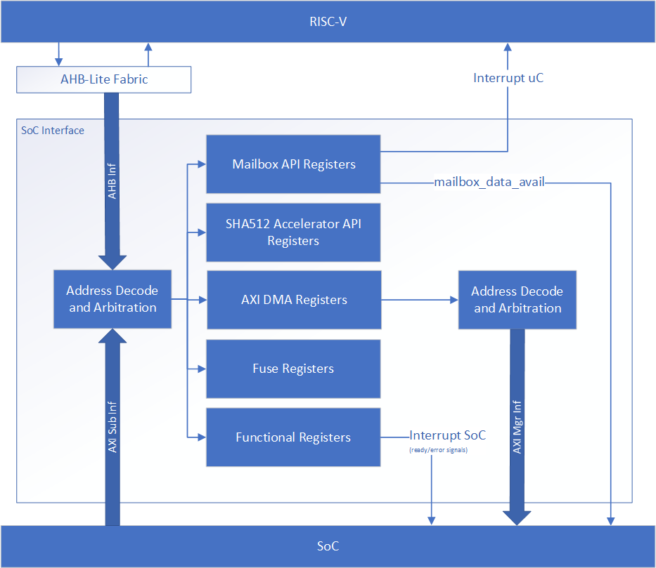
Integration parameters
The following table describes integration parameters.
Table 2: Integration parameters
| Parameter name | Width | Defines file | Description |
|---|---|---|---|
| CPTRA_SET_MBOX_AXI_USER_INTEG | 5 | soc_ifc_pkg.sv | Each bit hardcodes the valid AXI_USER for mailbox at integration time. |
| CPTRA_MBOX_VALID_AXI_USER | [4:0][31:0] | soc_ifc_pkg.sv | Each parameter corresponds to a hardcoded valid AXI_USER value for mailbox, set at integration time. Must set corresponding bit in the CPTRA_SET_MBOX_AXI_USER_INTEG parameter for this valid axi user override to be used. CANNOT use value 0xFFFFFFFF. This is reserved for Caliptra-internal usage. |
| CPTRA_DEF_MBOX_VALID_AXI_USER | 32 | soc_ifc_pkg.sv | Sets the default valid AXI_USER for mailbox accesses. This AXI_USER is valid at all times. CANNOT use value 0xFFFFFFFF. This is reserved for Caliptra-internal usage. |
| CPTRA_SET_FUSE_AXI_USER_INTEG | 1 | soc_ifc_pkg.sv | Sets the valid AXI_USER for fuse accesses at integration time. |
| CPTRA_FUSE_VALID_AXI_USER | 32 | soc_ifc_pkg.sv | Overrides the programmable valid AXI_USER for fuse accesses when CPTRA_SET_FUSE_AXI_USER_INTEG is set to 1. CANNOT use value 0xFFFFFFFF. This is reserved for Caliptra-internal usage. |
Table 3: Integration Defines
| Defines | Defines file | Description |
|---|---|---|
| CALIPTRA_FUSE_GRANULARITY_32 | config_defines.svh | Defining this means fuse row granularity is 32-bits. If not defined it means fuse row granularity is 64 bits. If defined, the CPTRA_HW_CONFIG.CALIPTRA_FUSE_GRANULARITY_32 SOC_IFC register bit is set to 1 for 32-bit granularity. Otherwise, it is set to 0 for 64-bit granularity. This is used by Caliptra ROM for UDS and Field Entropy provisioning. |
| CALIPTRA_INTERNAL_TRNG | config_defines.svh | Defining this enables the internal TRNG source. This is recommended to be set to 1 in Core (Passive) mode and must be set to 1 in Subsystem mode. |
| CALIPTRA_MODE_SUBSYSTEM | config_defines.svh | Defining this enables Caliptra to operate in Subsystem mode. This includes features such as the debug unlock flow, AXI DMA (for recovery flow), Subsystem-level straps, among other capabilites. See Caliptra Subsystem Architectural Flows for more details |
| USER_ICG | config_defines.svh | If added by an integrator, provides the name of the custom clock gating module that is used in clk_gate.sv. USER_ICG replaces the clock gating module, CALIPTRA_ICG, defined in caliptra_icg.sv. This substitution is only performed if integrators also define TECH_SPECIFIC_ICG. |
| TECH_SPECIFIC_ICG | config_defines.svh | Defining this causes the custom, integrator-defined clock gate module (indicated by the USER_ICG macro) to be used in place of the native Caliptra clock gate module. |
| USER_EC_RV_ICG | config_defines.svh | If added by an integrator, provides the name of the custom clock gating module that is used in the RISC-V core. USER_EC_RV_ICG replaces the clock gating module, TEC_RV_ICG, defined in beh_lib.sv. This substitution is only performed if integrators also define TECH_SPECIFIC_EC_RV_ICG. |
| TECH_SPECIFIC_EC_RV_ICG | config_defines.svh | Defining this causes the custom, integrator-defined clock gate module (indicated by the USER_EC_RV_ICG macro) to be used in place of the native RISC-V core clock gate module. |
| CALIPTRA_AXI_DMA_ADDR_WIDTH | config_defines.svh | Defines the address width for the Caliptra AXI Manager interface, driven by Caliptra's DMA assist block. The address width value assigned to this macro should match the address width that is expected at the integrator's SoC AXI interconnect. |
| CALIPTRA_PRIM_ROOT | environment variable | The integrator needs to set this environment variable to the path to technology specific modules for synthesis. Defaults to $CALIPTRA_ROOT/src/caliptra_prim_generic. |
| CALIPTRA_PRIM_MODULE_PREFIX | environment variable | The integrator needs to set this environment variable to specify the module name prefix for technology specific modules for synthesus. Defaults to 'caliptra_prim_generic'. |
Interface
The following tables describe the interface signals.
Table 4: Clocks and resets
| Signal name | Width | Driver | Synchronous (as viewed from Caliptra’s boundary) | Description |
|---|---|---|---|---|
| cptra_pwrgood | 1 | Input | Asynchronous Assertion Synchronous deassertion to clk | Active high power good indicator. Deassertion hard resets Caliptra. |
| cptra_rst_b | 1 | Input | Asynchronous Assertion Synchronous deassertion to clk | Active low asynchronous reset. |
| clk | 1 | Input | Convergence and validation done at 400MHz. All other frequencies are up to the user. |
Table 5: AXI Subordinate Interface
| Signal name | Width | Driver | Synchronous (as viewed from Caliptra’s boundary) | Description |
|---|---|---|---|---|
| araddr | AW | Input | Synchronous to clk | AR channel address |
| arburst | 2 | Input | Synchronous to clk | AR channel burst encoding |
| arsize | 3 | Input | Synchronous to clk | AR channel size encoding |
| arlen | 8 | Input | Synchronous to clk | AR channel length, beats in the burst |
| aruser | UW | Input | Synchronous to clk | AR channel user signal. Identifies the requester for mailbox and fuse access. See AXI_USER details for more information. |
| arid | IW | Input | Synchronous to clk | AR channel id signal |
| arlock | 1 | Input | Synchronous to clk | AR channel lock signal |
| arvalid | 1 | Input | Synchronous to clk | AR channel valid handshake signal |
| arready | 1 | Output | Synchronous to clk | AR channel ready handshake signal |
| rdata | DW | Output | Synchronous to clk | R channel read response data |
| rresp | 2 | Output | Synchronous to clk | R channel read response encoding |
| rid | IW | Output | Synchronous to clk | R channel read response id signal |
| ruser | UW | Output | Synchronous to clk | R channel read response user signal |
| rlast | 1 | Output | Synchronous to clk | R channel read response last beat signal |
| rvalid | 1 | Output | Synchronous to clk | R channel valid handhsake signal |
| rready | 1 | Input | Synchronous to clk | R channel ready handshake signal |
| awaddr | AW | Input | Synchronous to clk | AW channel address |
| awburst | 2 | Input | Synchronous to clk | AW channel burst encoding |
| awsize | 3 | Input | Synchronous to clk | AW channel size encoding |
| awlen | 8 | Input | Synchronous to clk | AW channel length, beats in the burst |
| awuser | UW | Input | Synchronous to clk | AW channel user signal. Identifies the requester for mailbox and fuse access. See AXI_USER details for more information. |
| awid | IW | Input | Synchronous to clk | AW channel id signal |
| awlock | 1 | Input | Synchronous to clk | AW channel lock signal |
| awvalid | 1 | Input | Synchronous to clk | AW channel valid handhsake signal |
| awready | 1 | Output | Synchronous to clk | AW channel ready handshake signal |
| wdata | DW | Input | Synchronous to clk | W channel write data |
| wuser | UW | Input | Synchronous to clk | W channel write user |
| wstrb | DW/8 | Input | Synchronous to clk | W channel write strobe. Byte enable. |
| wlast | 1 | Input | Synchronous to clk | W channel write last beat signal |
| wvalid | 1 | Input | Synchronous to clk | W channel valid handhsake signal |
| wready | 1 | Output | Synchronous to clk | W channel ready handshake signal |
| bresp | 2 | Output | Synchronous to clk | B channel write response encoding |
| bid | IW | Output | Synchronous to clk | B channel write response id signal |
| buser | UW | Output | Synchronous to clk | B channel write response user signal |
| bvalid | 1 | Output | Synchronous to clk | B channel valid handhsake signal |
| bready | 1 | Input | Synchronous to clk | B channel ready handshake signal |
Table 6: Mailbox notifications
| Signal name | Width | Driver | Synchronous (as viewed from Caliptra’s boundary) | Description |
|---|---|---|---|---|
| ready_for_fuses | 1 | Output | Synchronous to clk | Indicates that Caliptra is ready for fuse programming. |
| ready_for_mb_processing | 1 | Output | Synchronous to clk | Indicates that Caliptra is ready for processing mailbox commands. |
| ready_for_runtime | 1 | Output | Synchronous to clk | Indicates that Caliptra firmware is ready for RT flow. |
| mailbox_data_avail | 1 | Output | Synchronous to clk | Indicates that the mailbox has a response for SoC to read. Signal is set when the mailbox transitions to the EXECUTE_SOC state, which is also reported in the mbox_status register. |
| mailbox_flow_done | 1 | Output | Synchronous to clk | Deprecated output signal. Reflects the value from the CPTRA_FLOW_STATUS register field mailbox_flow_done, which is not used by firmware. For an indicator that Caliptra has completed its processing of the mailbox flow, an SoC may use the mailbox_data_avail signal. |
Table 7: Caliptra SRAM interface
| Signal name | Width | Driver | Synchronous (as viewed from Caliptra’s boundary) | Description |
|---|---|---|---|---|
| mbox_sram_cs | 1 | Output | Synchronous to clk | Chip select for mbox SRAM |
| mbox_sram_we | 1 | Output | Synchronous to clk | Write enable for mbox SRAM |
| mbox_sram_addr | MBOX_ADDR_W | Output | Synchronous to clk | Addr lines for mbox SRAM |
| mbox_sram_wdata | MBOX_DATA_W | Output | Synchronous to clk | Write data for mbox SRAM |
| mbox_sram_rdata | MBOX_DATA_W | Input | Synchronous to clk | Read data for mbox SRAM |
| imem_cs | 1 | Output | Synchronous to clk | Chip select for imem SROM |
| imem_addr | IMEM_ADDR_WIDTH | Output | Synchronous to clk | Addr lines for imem SROM |
| imem_rdata | IMEM_DATA_WIDTH | Input | Synchronous to clk | Read data for imem SROM |
| iccm_clken | ICCM_NUM_BANKS | Input | Synchronous to clk | Per-bank clock enable |
| iccm_wren_bank | ICCM_NUM_BANKS | Input | Synchronous to clk | Per-bank write enable |
| iccm_addr_bank | ICCM_NUM_BANKS x (ICCM_BITS-4) | Input | Synchronous to clk | Per-bank address |
| iccm_bank_wr_data | ICCM_NUM_BANKS x 32 | Input | Synchronous to clk | Per-bank input data |
| iccm_bank_wr_ecc | ICCM_NUM_BANKS x 7 | Input | Synchronous to clk | Per-bank input ecc |
| iccm_bank_dout | ICCM_NUM_BANKS x 32 | Output | Synchronous to clk | Per-bank output data |
| iccm_bank_ecc | ICCM_NUM_BANKS x 7 | Output | Synchronous to clk | Per-bank output ecc |
| dccm_clken | DCCM_NUM_BANKS | Input | Synchronous to clk | Per-bank clock enable |
| dccm_wren_bank | DCCM_NUM_BANKS | Input | Synchronous to clk | Per-bank write enable |
| dccm_addr_bank | DCCM_NUM_BANKS x (DCCM_BITS-4) | Input | Synchronous to clk | Per-bank address |
| dccm_wr_data_bank | DCCM_NUM_BANKS x DCCM_DATA_WIDTH | Input | Synchronous to clk | Per-bank input data |
| dccm_wr_ecc_bank | DCCM_NUM_BANKS x DCCM_ECC_WIDTH | Input | Synchronous to clk | Per-bank input ecc |
| dccm_bank_dout | DCCM_NUM_BANKS x DCCM_DATA_WIDTH | Output | Synchronous to clk | Per-bank output data |
| dccm_bank_ecc | DCCM_NUM_BANKS x DCCM_ECC_WIDTH | Output | Synchronous to clk | Per-bank output ecc |
Table 8: Adams-Bridge SRAM Interface
Adams-Bridge SRAM interface is used to connect the necessary SRAM instances for Adams-Bridge. There are 8 SRAMs, 2 of which have 2 banks. Each SRAM has a parameterized data width and depth used to calculate the addr width.
All memories are modeled as 1 read 1 write port RAMs with a flopped read data. See abr_1r1w_ram.sv and abr_1r1w_be_ram.sv for examples. Strobe width describes the number of bits enabled by each strobe. All strobed memories are byte enabled in the design. See ABR Memory requirement for more details.
The full set of wires is encapsulated in the abr_mem_if construct abr_memory_export at the Caliptra boundary.
The table below details the interface required for each SRAM. Driver direction is from the perspective of Caliptra.
| Signal name | Width | Driver | Synchronous (as viewed from Caliptra’s boundary) | Description |
|---|---|---|---|---|
| we_i | 1 | Output | Synchronous to clk | Write enable |
| waddr_i | ADDR_W | Output | Synchronous to clk | Write address |
| wdata_i | DATA_W | Output | Synchronous to clk | Write data |
| wstrobe_i | DATA_W/8 | Output | Synchronous to clk | Write strobe (only for sig_z and pk memories) |
| re_i | 1 | Output | Synchronous to clk | Read enable |
| raddr_i | ADDR_W | Output | Synchronous to clk | Read address |
| rdata_o | DATA_W | Input | Synchronous to clk | Read data |
Table 9: JTAG interface
| Signal name | Width | Driver | Synchronous (as viewed from Caliptra’s boundary) | Description |
|---|---|---|---|---|
| jtag_tck | 1 | Input | ||
| jtag_tms | 1 | Input | Synchronous to jtag_tck | |
| jtag_tdi | 1 | Input | Synchronous to jtag_tck | |
| jtag_trst_n | 1 | Input | Asynchronous assertion Synchronous deassertion to jtag_tck | |
| jtag_tdo | 1 | Output | Synchronous to jtag_tck |
Table 10: RISC-V Trace interface Trace ports have been directly connected from Caliptra's instance of the VeeR-EL2 RISC-V core to the top-level. However, use of these ports has not been validated. Integrators shall leave these ports unconnected. Support for these ports may be added in a future release.
| Signal name | Width | Driver | Synchronous (as viewed from Caliptra’s boundary) | Description |
|---|---|---|---|---|
| trace_rv_i_insn_ip | 32 | Output | Synchronous to clk | Trace signals from Caliptra RV core instance. Refer to VeeR documentation for more details. |
| trace_rv_i_address_ip | 32 | Output | Synchronous to clk | Trace signals from Caliptra RV core instance. Refer to VeeR documentation for more details. |
| trace_rv_i_valid_ip | 1 | Output | Synchronous to clk | Trace signals from Caliptra RV core instance. Refer to VeeR documentation for more details. |
| trace_rv_i_exception_ip | 1 | Output | Synchronous to clk | Trace signals from Caliptra RV core instance. Refer to VeeR documentation for more details. |
| trace_rv_i_ecause_ip | 5 | Output | Synchronous to clk | Trace signals from Caliptra RV core instance. Refer to VeeR documentation for more details. |
| trace_rv_i_interrupt_ip | 1 | Output | Synchronous to clk | Trace signals from Caliptra RV core instance. Refer to VeeR documentation for more details. |
| trace_rv_i_tval_ip | 32 | Output | Synchronous to clk | Trace signals from Caliptra RV core instance. Refer to VeeR documentation for more details. |
Table 11: Subsystem Straps, Controls, and iTRNG Configuration
| Signal name | Width | Driver | Synchronous (as viewed from Caliptra’s boundary) | Description |
|---|---|---|---|---|
| strap_ss_caliptra_base_addr | 64 | Input Strap | Synchronous to clk | Used in Subsystem mode only. In Passive mode, integrators shall tie this input to 0. |
| strap_ss_mci_base_addr | 64 | Input Strap | Synchronous to clk | Used in Subsystem mode only. In Passive mode, integrators shall tie this input to 0. |
| strap_ss_recovery_ifc_base_addr | 64 | Input Strap | Synchronous to clk | Used in Subsystem mode only. In Passive mode, integrators shall tie this input to 0. |
| strap_ss_external_staging_area_base_addr | 64 | Input Strap | Synchronous to clk | Used in Subsystem mode only. In Passive mode, integrators shall tie this input to 0. |
| strap_ss_otp_fc_base_addr | 64 | Input Strap | Synchronous to clk | Used in Subsystem mode only. In Passive mode, integrators shall tie this input to 0. |
| strap_ss_uds_seed_base_addr | 64 | Input Strap | Synchronous to clk | Used in Subsystem mode only. In Passive mode, integrators shall tie this input to 0. |
| strap_ss_key_release_base_addr | 64 | Input Strap | Synchronous to clk | Used in Subsystem mode only. This is the full destination address for MEK generated via OCP LOCK flow. In Passive mode, integrators shall tie this input to 0. |
| strap_ss_key_release_key_size | 64 | Input Strap | Synchronous to clk | Used in Subsystem mode only. This is the size of MEK generated via OCP LOCK flow. In Passive mode, integrators shall tie this input to 0. |
| strap_ss_prod_debug_unlock_auth_pk_hash_reg_bank_offset | 32 | Input Strap | Synchronous to clk | Used in Subsystem mode only. In Passive mode, integrators shall tie this input to 0. |
| strap_ss_num_of_prod_debug_unlock_auth_pk_hashes | 32 | Input Strap | Synchronous to clk | Used in Subsystem mode only. In Passive mode, integrators shall tie this input to 0. |
| strap_ss_caliptra_dma_axi_user | 32 | Input Strap | Synchronous to clk | Used in Subsystem mode only. In Passive mode, integrators shall tie this input to 0. |
| strap_ss_strap_generic_0 | 32 | Input Strap | Synchronous to clk | Used in Subsystem mode only. In Passive mode, integrators shall tie this input to 0. |
| strap_ss_strap_generic_1 | 32 | Input Strap | Synchronous to clk | Used in Subsystem mode only. In Passive mode, integrators shall tie this input to 0. |
| strap_ss_strap_generic_2 | 32 | Input Strap | Synchronous to clk | Provides Caliptra ROM with entropy source (CSRNG) configuration used during initialization when CALIPTRA_INTERNAL_TRNG is enabled, including Passive mode. If this configuration is not used, integrators shall tie this input to 0. |
| strap_ss_strap_generic_3 | 32 | Input Strap | Synchronous to clk | Used in Subsystem mode only. In Passive mode, integrators shall tie this input to 0. |
| ss_debug_intent | 1 | Input | Synchronous to clk | Sampled on cold reset. Used in Subsystem mode only. Indicates that the SoC is in debug mode and a user intends to request unlock of debug mode through the TAP mailbox. In Passive mode, integrators shall tie this input to 0. |
| ss_ocp_lock_en | 1 | Input | Synchronous to clk | Sampled on cold reset. Used in Subsystem mode only. Indicates that the SoC enables OCP LOCK features of Caliptra. Must be tied to a constant value. For example, driving this input from a programmable register or from a package pin is not permitted. |
| ss_dbg_manuf_enable | 1 | Output | Synchronous to clk | Enables unlock of the debug interface in the Manufacturing security state, for Subsystem mode only. |
| ss_soc_dbg_unlock_level | 64 | Output | Synchronous to clk | Enables unlock of the debug interface in the Production security state, for Subsystem mode only. |
| ss_generic_fw_exec_ctrl | 128 | Output | Synchronous to clk | Enables SoC processors to execute firmware once authenticated by Caliptra. |
| recovery_data_avail | 1 | Input | Synchronous to clk | Input from streaming boot interface (a.k.a. recovery interface) indicating that a payload is available in the data buffer. |
| recovery_image_activated | 1 | Input | Synchronous to clk | Input from streaming boot interface (a.k.a. recovery interface) indicating that firmware image is activated. |
Table 12: Security and miscellaneous
| Signal name | Width | Driver | Synchronous (as viewed from Caliptra’s boundary) | Description |
|---|---|---|---|---|
| cptra_obf_key | 256 | Input Strap | Asynchronous | Obfuscation key is driven by SoC at integration time. Ideally this occurs just before tape-in and the knowledge of this key must be protected unless PUF is driving this. The key is latched by Caliptra upon first deassertion of the warm reset following caliptra powergood assertion. It is not resampled during subsequent warm resets, therefore the value is only captured upon a cold boot. It is cleared after its use and can only re-latched on a power cycle (powergood deassertion to assertion). |
| cptra_csr_hmac_key | 512 | Input Strap | Asynchronous | CSR HMAC key is driven by SoC at integration time. Ideally this occurs just before tape-in and the knowledge of this key must be protected. The key is latched by Caliptra following deassertion of the noncore warm reset during DEVICE_MANUFACTURING lifecycle state. This key input is ignored in all other lifecycle states. |
| cptra_obf_field_entropy_vld | 1 | Input | Synchronous to clk | Used in Subsystem mode only. In Passive mode, integrators shall tie this input to 0. Valid signal used to sample cptra_obf_field_entropy if it is driven by wires from the fuse controller. |
| cptra_obf_field_entropy | 256 | Input | Synchronous to clk | Used in Subsystem mode only. In Passive mode, integrators shall tie this input to 0. Fuse controller can optionally drive the field entropy value over wires through this interface. The value is sampled after warm reset if the valid cptra_obf_field_entropy_vld is asserted. |
| cptra_obf_uds_seed_vld | 1 | Input | Synchronous to clk | Used in Subsystem mode only. In Passive mode, integrators shall tie this input to 0. Valid signal used to sample cptra_obf_uds_seed if it is driven by wires from the fuse controller. |
| cptra_obf_uds_seed | 512 | Input | Synchronous to clk | Used in Subsystem mode only. In Passive mode, integrators shall tie this input to 0. Fuse controller can optionally drive the uds seed value over wires through this interface. The value is sampled after warm reset if the valid cptra_obf_uds_seed_vld is asserted. |
| security_state | 3 | Input Strap | Synchronous to clk | Security state that Caliptra should take (for example, manufacturing, secure, unsecure, etc.). The key is latched by Caliptra on cptra_noncore_rst_b deassertion. Any time the state changes to debug mode, all keys, assets, and secrets stored in fuses or key vault are cleared. Cryptography core states are also flushed if they were being used. |
| scan_mode | 1 | Input Strap | Synchronous to clk | Must be set before entering scan mode. This is a separate signal than the scan chain enable signal that goes into scan cells. This allows Caliptra to flush any assets or secrets present in key vault and flops if the transition is happening from a secure state. |
| generic_input_wires | 64 | Input | Synchronous to clk | Placeholder of input wires for late binding features. These values are reflected into registers that are exposed to firmware. |
| generic_output_wires | 64 | Output | Synchronous to clk | Placeholder of output wires for late binding features. Firmware can set the wires appropriately via register writes. |
| cptra_error_fatal | 1 | Output | Synchronous to clk | Indicates a fatal error from Caliptra. |
| cptra_error_non_fatal | 1 | Output | Synchronous to clk | Indicates a non fatal error from Caliptra. |
| BootFSM_BrkPoint | 1 | Input Strap | Asynchronous | Stops the BootFSM to allow TAP writes set up behavior. Examples of these behaviors are skipping or running ROM flows, or stepping through BootFSM. |
| etrng_req | 1 | Output | Synchronous to clk | External source mode: TRNG_REQ to SoC. SoC writes to TRNG architectural registers with a NIST-compliant entropy. Internal source mode: TRNG_REQ to SoC. SoC enables external RNG digital bitstream input into itrng_data/itrng_valid. |
| itrng_data | 4 | Input | Synchronous to clk | External source mode: Not used. Internal source mode only: Physical True Random Noise Source (PTRNG for "Number Generator") digital bit stream from SoC, which is sampled when itrng_valid is high. See the Hardware Specification for details on PTRNG expectations and iTRNG entropy capabilities. |
| itrng_valid | 1 | Input | Synchronous to clk | External source mode: Not used. Internal source mode only: RNG bit valid. This is valid per transaction. itrng_data can be sampled whenever this bit is high. The expected itrng_valid output rate is dependent on the process node technology. For 40nm, it is expected to be at least 50kHz. For latest industry standard, moderately advanced technology, it is expected to be greater than 400kHz. |
Architectural registers and fuses
Control registers and fuses are documented on GitHub.
- External Registers: caliptra_top_reg — caliptra_top_reg Reference (chipsalliance.github.io)
- Internal Registers - clp — clp Reference (chipsalliance.github.io)
Fuses
Fuses may only be written during the BOOT_FUSE state of the Boot FSM and require a cptra_pwrgood to be recycled to be written again.
After all fuses are written, the fuse done register at the end of the fuse address space must be set to 1 to lock the fuse writes and to proceed with the boot flow.
Although fuse values (and the fuse done register) persist across a warm reset, SoC is still required to perform a write to the fuse done register while in the BOOT_FUSE state in order to complete the bringup from reset. See Boot FSM for further details.
Note: Starting in Caliptra 2.0 subsystem strap and other configuration registers have been added to the fuse region. Subsystem straps are expected to be programmed during the same time as fuses per Caliptra spec. The following SS registers in the fuse region are not straps, are intended for internal use in Caliptra, and cannot be written by any SoC agents; therefore, categorizing them under the FUSE range has no effect:
SS_DBG_SERVICE_REG_RSPSS_SOC_DBG_UNLOCK_LEVELSS_GENERIC_FW_EXEC_CTRL
The remaining register SS_DBG_SERVICE_REG_REQ is initialized by the same SoC agent as fuses and is the only agent that can make subsystem debug service requests.
FUSE AXI USER attribute
The CPTRA_FUSE_VALID_AXI_USER attribute is used to restrict access to the fuse registers via AXI to a single permitted SoC configuration agent. It is strongly recommended that the CPTRA_FUSE_VALID_AXI_USER value is either set at integration time through integration parameters or be programmed by the SoC ROM via register write before any mutable firmware or ROM patches are applied.
SoC SHALL not use value 0xFFFFFFFF as a valid AXI user value for any of the below settings. This is reserved for Caliptra-internal usage.
FUSE AXI USER Programmable register
Caliptra provides 1 programmable register that SoC can set at boot time to limit access to the fuse register set. If the CPTRA_FUSE_AXI_USER_LOCK.LOCK is set to ‘0, then access to the fuse registers by any agent is allowed. If the lock is set to ‘1, only an agent whose AXI USER matches the register CPTRA_FUSE_VALID_AXI_USER.AXI_USER can write to fuse registers. Any access by an unallowed AXI USER will return an AXI error response. CPTRA_FUSE_VALID_AXI_USER registers become valid once the corresponding lock bit CPTRA_FUSE_AXI_USER_LOCK.LOCK is set.
FUSE AXI USER Parameter override
Another option for limiting access to the fuse registers is the integration time parameter, which overrides the programmable AXI_USER register. At integration time, the CPTRA_SET_FUSE_AXI_USER_INTEG parameter can be set to 1 which enables the corresponding CPTRA_FUSE_VALID_AXI_USER parameter to override the programmable register. If CPTRA_SET_FUSE_AXI_USER_INTEG is set to ‘0, then access to the fuse registers by any agent is allowed. If this parameter is set to ‘1, only an agent whose AXI USER matches the parameter CPTRA_FUSE_VALID_AXI_USER can write to fuse registers. Any access by an unallowed AXI USER will return an AXI error response.
Interface rules
The following figure shows the reset rules and timing for cold boot flows.
Figure: Reset rules and timing diagram
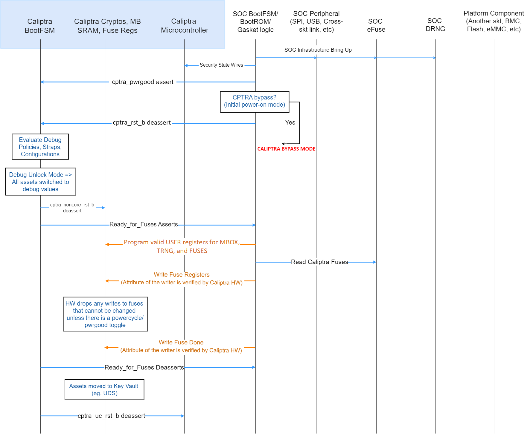
Deassertion of cptra_pwrgood indicates a power cycle that results in returning Caliptra to its default state. All resettable flops are reset.
Deassertion of cptra_rst_b indicates a warm reset cycle that resets all but the “sticky” registers (fuses, error logging, etc.).
Assertion of BootFSM_BrkPoint stops the boot flow from releasing Caliptra from reset after fuse download. Writing a 1 to the GO field of the CPTRA_BOOTFSM_GO register allows the boot flow to proceed.
AXI
Arbitration
Caliptra has two interfaces attached to the AXI bus: a subordinate, incapable of initiating transfers, and a manager interface. The AXI manager is only enabled in Caliptra Subsystem mode, and must be tied to 0 in all other use-cases. The AXI subordinate is used by SoC agents to interact with the Caliptra external registers. If SoCs have multiple AXI agents or other proprietary-fabric protocols that require any special fabric arbitration, that arbitration is done at SoC level.
AXI User
AXI address user request signals (ARUSER and AWUSER, collectively "AxUSER") are used to uniquely identify AXI agents that have issued the request to Caliptra. Refer to Mailbox AXI User Attribute Register and SoC Integration Requirements for additional details.
Unsupported features
The Caliptra AXI subordinate has the following usage restrictions:
- Single outstanding transaction is serviced at a time (read or write). Operation is half-duplex due to the underlying register access interface.
- AXI read and write requests may be accepted simultaneously by the AXI subordinate, but internal arbitration will service them one at a time.
- Responses are in order
- Burst data interleaving is not supported
- SoC agents shall not initiate AXI burst transfers to the SoC interface, except as write bursts to the mbox_datain register or read bursts from the mbox_dataout register. Such bursts shall be of the AXI "FIXED" burst type.
- Accesses to these registers shall not be "narrow". This means that AxSIZE must be set to 0x2 and WSTRB must be set to 0xF.
- mbox_datain
- mbox_dataout
- CPTRA_TRNG_DATA
- Violations of the AXI specification by AXI managers will result in undefined behavior. Examples include:
- AxSIZE values larger than interface width (greater than 0x2).
- AxLEN larger than legal value (256 maximum burst size, 16 for FIXED bursts, and total burst length must be 4096 Bytes or less).
- Number of data beats on W channel does not match burst length indicated on AWLEN.
- RRESP or BRESP has an undefined value.
- WLAST is driven incorrectly, driven on multiple beats, or never driven.
- Exclusive accesses are not supported. I.e. AxLOCK must be tied to 0.
- The following signals are unused/unconnected:
- AxCACHE
- AxPROT
- AxREGION
- AxQOS
Undefined address accesses
All accesses that are outside of the defined address space of Caliptra are responded to by Caliptra’s SoC interface:
- All reads to undefined addresses get completions with zero data.
- All writes to undefined addresses are dropped.
- All other undefined opcodes are silently dropped.
- Access to mailbox memory region with invalid AXI_USER are dropped.
- Access to a fuse with invalid AXI_USER are dropped.
- Access to the trng with invalid AXI_USER are dropped.
- SLVERR is asserted for any of the above conditions.
All accesses must be 32-bit aligned. Misaligned writes are dropped and reads return 0x0.
DMA Assist Engine
Caliptra contains a DMA assist engine and AXI manager interface that is used in Subsystem mode to initiate AXI transactions to the SoC AXI interconnect. When Caliptra is integrated in passive mode the DMA assist block is not available for use; all AXI manager interfaces must be tied to 0 and must not be connected to the SoC interconnect. For details on the DMA block in Subsystem mode operation, refer to the Caliptra Subsystem Hardware Specification.
Undefined mailbox usages
A trusted/valid requester that locks the mailbox and never releases the lock will cause the mailbox to be locked indefinitely.
Caliptra firmware internally has the capability to force release the mailbox based on various timers but there is no architectural requirement to use this capability.
Straps
Straps are signal inputs to Caliptra that are sampled once on reset exit, and the latched value persists throughout the remaining uptime of the system. Straps are sampled on either cptra_pwrgood signal assertion (cold reset exit) or cptra_noncore_rst_b deassertion (warm reset exit) – refer to interface table for list of straps. In 2.0, Caliptra adds support for numerous Subsystem-level straps. These straps are initialized on warm reset deassertion to the value from the external port, but may also be rewritten by the SoC firmware at any time prior to CPTRA_FUSE_WR_DONE being set. These must be programmed by SoC FW at the same time as Caliptra Fuses per Caliptra Spec. Once written and locked, the values of these straps persist until a cold reset.
Obfuscation key
SoC drives the key at the tape-in time of the SoC using an Engineering Change Order (ECO) and must be protected from common knowledge. For a given SoC construction, this can be driven using a PUF too.
The key must follow the security rules defined in the SOC integration requirements.
SoC must ensure that there are no SCAN cells on the flops that latch this key internally to Caliptra.
CSR HMAC key
SoC drives the key at the tape-in time of the SoC using an Engineering Change Order (ECO) and must be protected from common knowledge.
The key must follow the security rules defined in the SOC integration requirements.
SoC must ensure that there are no SCAN cells on the flops that latch this key internally to Caliptra.
Late binding interface signals
The interface signals generic_input_wires, generic_output_wires, and strap_ss_strap_generic_N are placeholders on the SoC interface reserved for late binding features. This may include any feature that is required for correct operation of the design in the final integrated SoC and that may not be accommodated through existing interface signaling (such as the mailbox).
While these late binding interface pins are generic in nature until assigned a function, integrators must not define non-standard use cases for these pins. Defining standard use cases ensures that the security posture of Caliptra in the final implementation is not degraded relative to the consortium design intent. Bits in generic_input_wires and strap_ss_strap_generic_N that don't have a function defined in Caliptra must be tied to a 0-value. These undefined input bits shall not be connected to any flip flops (which would allow run-time transitions on the value).
Each wire connects to a register in the SoC Interface register bank through which communication to the internal microprocessor may be facilitated. Each of the generic wire signals is 64 bits in size. The size of the generic strap is indicated in Table 11.
Activity on any bit of the generic_input_wires triggers a notification interrupt to the microcontroller indicating a bit toggle.
The following table describes the allocation of functionality on generic_input_wires. All bits not listed in this table must be tied to 0.
Table 13: generic_input_wires function binding
| Bit | Name | Description |
|---|---|---|
| 0 | Zeroization status | Used by SoC to provide zeroization status of fuses. |
| 63:1 | RESERVED | No allocated function. |
The following table describes the allocation of functionality to strap_ss_strap_generic_N. All straps not listed in this table must be tied to 0.
Table 14: strap_ss_strap_generic_N function binding
| N | Name | Description |
|---|---|---|
| 0 | strap_ss_strap_generic_0 | Provides the Caliptra ROM with a 32-bit pointer that encodes the location of the fuse controller's status register and the bit position of the idle indicator. Upper 16 bits: Bit index of the IDLE_BIT_STATUS within SOC_OTP_CTRL_STATUS. Lower 16 bits: Offset address of SOC_OTP_CTRL_STATUS within the SOC_IFC_REG space, relative to SOC_OTP_CTRL_BASE_ADDR. |
| 1 | strap_ss_strap_generic_1 | Provides the Caliptra ROM with a 32-bit pointer to the fuse controller’s command register (CMD), enabling ROM-level control or triggering of fuse operations. |
| 2 | strap_ss_strap_generic_2 | Provides the Caliptra ROM with entropy source (CSRNG) configuration used during initialization when CALIPTRA_INTERNAL_TRNG is enabled, including Passive mode. Bits [15:0]: Health test window size for FIPS mode. This is the window size for all health tests when entropy is tested in FIPS mode. In single-bit mode, the entropy source internally tests four times this many samples on the selected lane. Bit [16]: Entropy source single-bit mode. ROM clears threshold_scope during entropy source initialization. When this bit is set to 1, ROM enables rng_bit_enable. Bits [18:17]: Entropy source single-bit mode rng_bit_sel. Selects which RNG bit stream to process when single-bit mode is enabled. Bits [30:19]: RESERVED/unused, must be tied to 0. Bit [31]: Entropy bypass mode. When set to 1, enables bypass mode (es_type) to allow entropy characterization directly without passing through conditioning. Refer to the Caliptra ROM Specification for additional details. |
| 3 | strap_ss_strap_generic_3 | Provides the Caliptra ROM with Stable Owner Key controls. Bit [0]: Stable Owner Key enable. When set to 1, ROM derives the Stable Owner Root Key from the HEK seed and allows CM_DERIVE_STABLE_KEY with key_type = OwnerKey when the other availability requirements are met (subsystem mode active and OCP LOCK disabled). When clear, Stable Owner Key derivation is disabled. Bits [31:1]: RESERVED/unused, must be tied to 0. Refer to the Caliptra ROM Specification for additional details. |
SoC interface operation
The Caliptra mailbox is the primary communication method between Caliptra and the SoC that Caliptra is integrated into.
The Caliptra mailbox uses an AXI interface to communicate with the SoC. The SoC can write to and read from various memory mapped register locations over the AXI interface in order to pass information to Caliptra.
Caliptra in turn also uses the mailbox to pass information back to the SoC. The interface does not author any transaction on the AXI interface. The interface only signals to the SoC that data is available in the mailbox and it is the responsibility of the SoC to read that data from the mailbox.
Boot FSM
The Boot FSM detects that the SoC is bringing Caliptra out of reset. Part of this flow involves signaling to the SoC that Caliptra is ready for fuses. After fuses are populated and the SoC indicates that it is done downloading fuses, the boot FSM wakes up the rest of Caliptra by deasserting the internal reset. Refer to CaliptraHardwareSpecification.md for more details and diagrams.
The boot FSM first waits for the SoC to assert cptra_pwrgood and deassert cptra_rst_b. The SoC first provides a stable clock to Caliptra. After a minimum of 10 clock cycles have elapsed on the stable clock, the SoC asserts cptra_pwrgood. The SoC waits for a minimum of 10 clocks after asserting cptra_pwrgood before deasserting cptra_rst_b. In the BOOT_FUSE state, Caliptra signals to the SoC that it is ready for fuses. After the SoC is done writing fuses, it sets the fuse done register and the FSM advances to BOOT_DONE.
BOOT_DONE enables Caliptra reset deassertion through a two flip-flop synchronizer.
SoC access mechanism
The SoC communicates with the mailbox through an AXI Interface. The SoC acts as the requester with the Caliptra mailbox as the receiver.
The AXI_USER bits are used by the SoC to identify which device is accessing the mailbox.
External Staging Area
To save SRAM area when Caliptra operates in Subsystem mode, the mailbox (MBOX) SRAM is reduced to 16 KiB.
Instead of passing images directly to Caliptra through the mailbox, the SoC can configure an external staging SRAM that Caliptra fetches from and processes.
Caliptra Core receives the base address of this staging area through the SOC_IFC register SS_EXTERNAL_STAGING_AREA_BASE_ADDR. The address must be an AXI address accessable via the Caliptra DMA controller. This register is exposed as a strap strap_ss_external_staging_area_base_addr and is overridable by SW until FUSE_DONE is set.
For hitless updates or other image-processing operations, the Caliptra mailbox should be used to:
- Notify Caliptra that an image is available for processing.
- Specify the command to run on the image.
- Indicate the size of the image in the staging area.
References:
The external staging area must be within the Caliptra crypto boundary. Meaning there must be access restrictions similar to the MBOX preventing trusted entities from manipulating or accessing the data being processed by Caliptra.
Mailbox
The Caliptra mailbox is a 256 KiB when in passive mode and 16 KiB when in subsystem mode buffer used for exchanging data between the SoC and the Caliptra microcontroller. See External Staging Area why the MBOX SRAM size is smaller in subsystem mode.
When a mailbox is populated by the SoC, initiation of the operation by writing the execute bit triggers an interrupt to the microcontroller. This interrupt indicates that a command is available in the mailbox. The microcontroller is responsible for reading from and responding to the command.
When a mailbox is populated by the microcontroller, an output wire to the SoC indicates that a command is available in the mailbox. The SoC is responsible for reading from and responding to the command.
Mailboxes are generic data-passing structures with a specific protocol that defines legal operations. This protocol for writing to and reading from the mailbox is enforced in hardware as described in the Caliptra mailbox errors section. How the command and data are interpreted by the microcontroller and SoC are not enforced in this specification.
Sender Protocol
Sending data to the mailbox:
- Requester queries the mailbox by reading the LOCK control register.
- If LOCK returns 0, LOCK is granted and will be set to 1.
- If LOCK returns 1, MBOX is locked for another device.
- Requester writes the command to the COMMAND register.
- Requester writes the data length in bytes to the DLEN register.
- Requester writes data packets to the MBOX DATAIN register.
- Requester writes to the EXECUTE register.
- Requester reads the STATUS register. Status can return:
- CMD_BUSY - 2’b00 – Indicates the requested command is still in progress
- DATA_READY - 2’b01 – Indicates the return data is in the mailbox for requested command
- CMD_COMPLETE- 2’b10 – Indicates the successful completion of the requested command
- CMD_FAILURE- 2’b11 – Indicates the requested command failed
- Requester reads the response if DATA_READY was the status.
- Requester resets the EXECUTE register to release the lock.
Notes on behavior:
Once LOCK is granted, the mailbox is locked until that device has concluded its operation. Caliptra has access to an internal mechanism to terminate a lock early or release the lock if the device does not proceed to use it or to recover from deadlock scenarios. If used, the force unlock mechanism has several effects:
- Returns the mailbox FSM (indicated in the mbox_status register) to the IDLE state.
- Resets the status field of the mbox_status register to CMD_BUSY.
- Resets the soc_has_lock field of the mbox_status register to 0.
- If the mailbox was in the ERROR state, internal hardware would continuously assert the error interrupt signals as described in Caliptra mailbox errors. The force unlock mechanism causes hardware to stop asserting these conditions, though any interrupts that are already asserted remain asserted and require firmware intervention to be cleared.
To address these conditions, integrators may wish to add timeout handling logic to their implementation of the mailbox protocol. This timeout handling logic may determine that a pending mailbox request has been terminated by observing the deassertion of mbox_status.soc_has_lock, or by observing that mbox_status.mbox_fsm_ps indicates the IDLE state. Upon observing these conditions, SoC logic may check for any error conditions reported in CPTRA_HW_ERROR_FATAL or CPTRA_HW_ERROR_NON_FATAL, and may attempt a retry of the command depending on any SoC retry policies.
The following figure shows the sender protocol flow.
Figure: Sender protocol flow chart
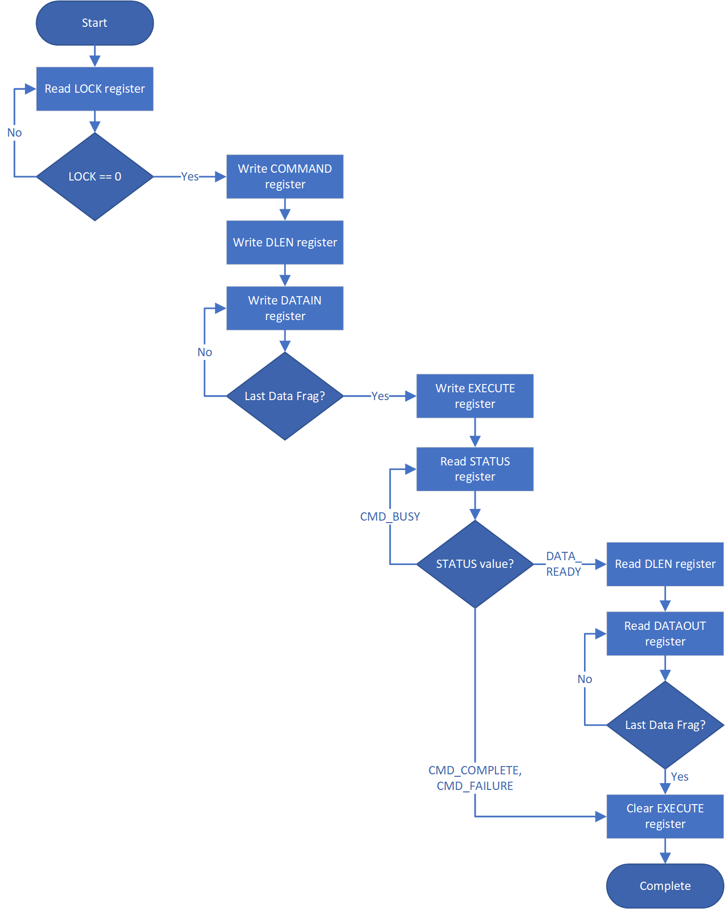
Receiver Protocol
Upon receiving indication that mailbox has been populated, the appropriate device can read the mailbox. This is indicated by a dedicated wire that is asserted when Caliptra populates the mailbox for SoC consumption.
Caliptra will not initiate any mailbox commands that require a response from the SoC. Caliptra initiated mailbox commands are “broadcast” and available to any user on the SoC. SoC will not be able to write the DLEN or DATAIN register while processing a Caliptra initiated mailbox command.
Receiving data from the mailbox:
- On mailbox_data_avail assertion, the receiver reads the COMMAND register.
- Receiver reads the DLEN register.
- Receiver reads the CMD register.
- Receiver reads the MBOX DATAOUT register.
- Continue reading MBOX DATAOUT register until DLEN bytes are read.
- If a response is required, the receiver can populate the mailbox with the response by updating the DLEN register and writing to DATAIN with the response. (NOTE: The new DLEN value will not take effect until control is returned to the sender via write to the status register).
- Set the mailbox status register appropriately to hand control back to the sender.
- The sender will reset the EXECUTE register.
- This releases the LOCK on the mailbox.
The following figure shows the receiver protocol flow.
Figure: Receiver protocol flowchart
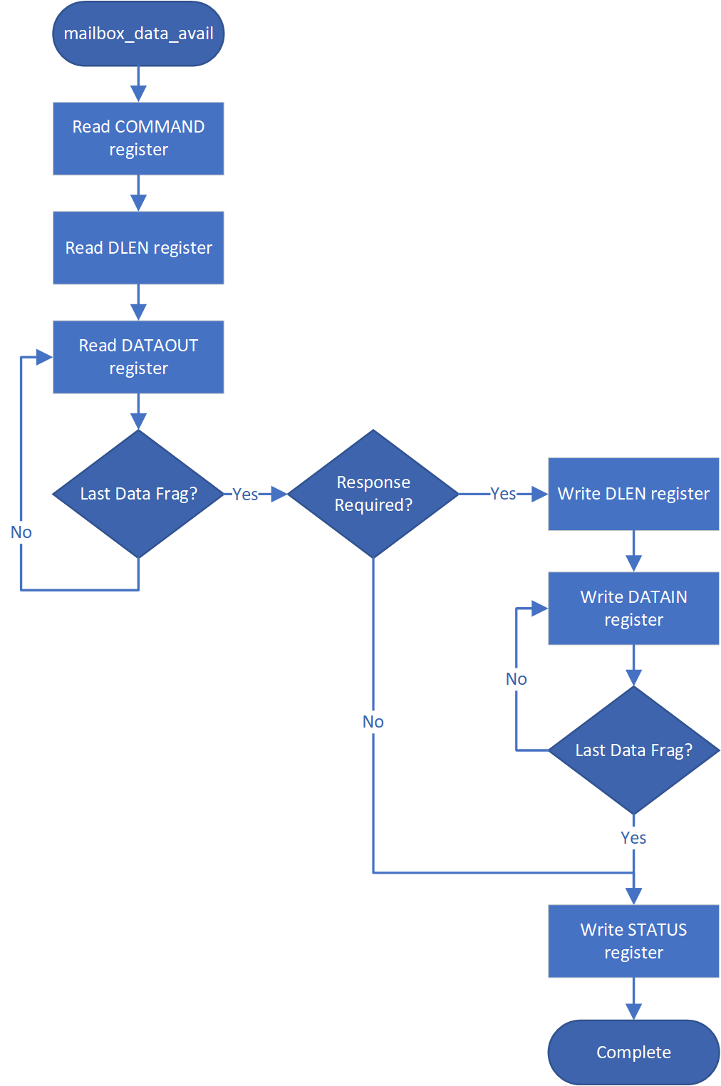
TAP mailbox mode
When Caliptra sets the tap_mode register, the mailbox will transition from RDY_FOR_DATA to EXECUTE_TAP instead of EXECUTE_SOC. This will pass control of the mailbox to the TAP. TAP will follow the Receiving data from the mailbox protocol detailed above.
When TAP acquires the mailbox lock, the mailbox will transition from RDY_FOR_DATA_to EXECUTE_UC. This transition results in the assertion of the internal interrupt signal uc_mailbox_data_avail to UC.
This will pass control of the mailbox to the UC. UC will follow the Receiving data from the mailbox protocol detailed above.
Mailbox arbitration
From a mailbox protocol perspective, as long as CPTRA_VALID_AXI_USER registers carry valid requesters, mailbox lock can be obtained by any of those valid requesters but only one of them at any given time. While the mailbox flow is happening, all other requesters will not get a grant.
A request for lock that is denied due to firmware having the lock results in an interrupt to the firmware. Firmware can optionally use this interrupt to release the lock.
There is no fair arbitration scheme between SoC and microcontroller. It is first come, first served. When the mailbox is locked for microcontroller use and SoC has unsuccessfully requested the mailbox (due to mailbox actively being used), the mailbox generates an interrupt to the microcontroller as a notification.
Further, there is no arbitration between various AXI_USER attributes. AXI_USER attributes exist for security and filtering reasons only.
MAILBOX AXI USER attribute register
It is strongly recommended that these AXI_USER registers are either set at integration time through integration parameters or be programmed by the SoC ROM before any mutable firmware or ROM patches are applied.
SoC SHALL not use value 0xFFFFFFFF as a valid AXI user value for any of the below settings. This is reserved for Caliptra-internal usage.
Programmable registers
Caliptra provides 5 programmable registers that SoC can set at boot time to limit access to the mailbox peripheral. The default AXI_USER set by the integration parameter CPTRA_DEF_MBOX_VALID_AXI_USER is valid at all times. CPTRA_MBOX_VALID_AXI_USER registers become valid once the corresponding lock bit CPTRA_MBOX_AXI_USER_LOCK is set.
Table 15: AXI_USER register definition
| Register | Description |
|---|---|
| CPTRA_MBOX_VALID_AXI_USER[4:0][31:0] | 5 registers for programming AXI_USER values that are considered valid for accessing the mailbox protocol. Requests with AXI_USER attributes that are not in this list will return an AXI error response. |
| CPTRA_MBOX_AXI_USER_LOCK[4:0] | 5 registers, bit 0 of each locks the corresponding VALID_AXI_USER register and marks it VALID. |
Parameter override
Another option for limiting access to the mailbox peripheral are the integration time parameters that override the programmable AXI_USER registers. At integration time, the CPTRA_SET_MBOX_AXI_USER_INTEG parameters can be set to 1 which enables the corresponding CPTRA_MBOX_VALID_AXI_USER parameters to override the programmable register.
Table 16: AXI_USER Parameter definition
| Parameter | Description |
|---|---|
| CPTRA_SET_MBOX_AXI_USER_INTEG[4:0] | Setting to 1 enables the corresponding CPTRA_MBOX_VALID_AXI_USER parameter. |
| CPTRA_MBOX_VALID_AXI_USER[4:0] | Value to override programmable AXI_USER register at integration time if corresponding CPTRA_SET_MBOX_AXI_USER_INTEG parameter is set to 1. |
Caliptra mailbox protocol
After the SoC side has written the EXECUTE register, the mailbox sends an interrupt to the microcontroller.
The microcontroller reads the COMMAND and DLEN registers, as well as the data populated in the mailbox.
The microcontroller can signal back to SoC through functional registers, and populate COMMAND, DLEN, and MAILBOX as well.
Caliptra mailbox errors
Mailbox is responsible for only accepting writes from the device that requested and locked the mailbox.
If the SoC violates this protocol, the mailbox flags a protocol violation and enters an error state. Two protocol violations are detected:
- Access without lock: Writes to any mailbox register by SoC or reads from the dataout register, without having first acquired the lock, are a violation.
- If any agent currently has the lock, accesses by agents other than the one holding the lock are ignored.
- If no agent currently has the lock, the violation results in a flagged error.
- Out of order access: SoC must follow the rules for the sender and receiver protocol that define access ordering and progression for a mailbox command.
- If, after acquiring the lock, an SoC agent performs any register write (or read from the dataout register) outside of the prescribed ordering, this is a flagged violation.
- Such access by any SoC agent that does not have the lock is ignored.
After a mailbox protocol violation is flagged, it is reported to the system in several ways:
-
The mailbox FSM enters the ERROR state in response to an out of order access violation, and the new FSM state is readable via the mailbox status register. The LOCK value is preserved on entry to the ERROR state. The access without lock violation does not result in a state change. After entering the ERROR state, the mailbox may only be restored to the IDLE state by:
- System reset
- Write to the force unlock register by firmware inside Caliptra (via internal bus)
Either of these mechanisms will also clear the mailbox LOCK.
-
Mailbox protocol violations are reported as fields in the HW ERROR non-fatal register. These events also cause assertion of the cptra_error_non_fatal interrupt signal to SoC. Upon detection, SoC may acknowledge the error by clearing the error field in this register via bus write.
-
Mailbox protocol violations generate an internal interrupt to the Caliptra microcontroller. Caliptra firmware is aware of the protocol violation.
The following table describes AXI transactions that cause the Mailbox FSM to enter the ERROR state, given that the register “mbox_user” contains the value of the AXI USER that was used to originally acquire the mailbox lock.
Table 17: Mailbox protocol error trigger conditions
| FSM state | SoC HAS LOCK | AXI USER eq mbox_user | Error state trigger condition |
|---|---|---|---|
| MBOX_RDY_FOR_CMD | 1 | true | Read from mbox_dataout. Write to any register other than mbox_cmd. |
| MBOX_RDY_FOR_CMD | 1 | false | - |
| MBOX_RDY_FOR_CMD | 0 | - | - |
| MBOX_RDY_FOR_DLEN | 1 | true | Read from mbox_dataout. Write to any register other than mbox_dlen. |
| MBOX_RDY_FOR_DLEN | 1 | false | - |
| MBOX_RDY_FOR_DLEN | 0 | - | - |
| MBOX_RDY_FOR_DATA | 1 | true | Read from mbox_dataout. Write to any register other than mbox_datain or mbox_execute. |
| MBOX_RDY_FOR_DATA | 1 | false | - |
| MBOX_RDY_FOR_DATA | 0 | - | - |
| MBOX_EXECUTE_UC | 1 | true | Read from mbox_dataout. Write to any register. |
| MBOX_EXECUTE_UC | 1 | false | - |
| MBOX_EXECUTE_UC | 0 | - | - |
| MBOX_EXECUTE_SOC | 1 | true | Write to any register other than mbox_execute. |
| MBOX_EXECUTE_SOC | 1 | false | - |
| MBOX_EXECUTE_SOC | 0 | true/false* | Write to any register other than mbox_status. |
* mbox_user value is not used when Caliptra has lock and is sending a Caliptra to SoC mailbox operation.
SoC SHA acceleration block
Overview
The SHA acceleration block is in the SoC interface. The SoC can access the accelerator’s hardware API and stream data to be hashed over the AXI interface.
SHA acceleration block uses a similar protocol to the mailbox, but has its own dedicated registers. Caliptra is the only permitted user of SHA acceleration, either in streaming mode (via AXI) or in mailbox mode. Use of the SHA acceleration block over AXI is only available in Caliptra Subsystem, and is only available to Caliptra, which will access it via the AXI DMA block. The SHA accelerator checks the AXI AxUSER signal to block any access that originates from an agent other than Caliptra's AXI DMA.
SHA_LOCK register is set on read. A read of 0 indicates the SHA was unlocked and will now be locked for the requesting user.
SHA_MODE register sets the mode of operation for the SHA.
See the Hardware specification for additional details.
- 2’b00 - SHA384 streaming mode
- 2’b01 - SHA512 streaming mode
- 2’b10 - SHA384 mailbox mode (Caliptra only, invalid for SoC requests)
- 2’b11 - SHA512 mailbox mode (Caliptra only, invalid for SoC requests)
SoC Sender Protocol
Sending data to the SHA accelerator:
- Requester queries the accelerator by reading the SHA_LOCK control register.
- If SHA_LOCK returns 0, SHA_LOCK is granted and is set to 1.
- If SHA_LOCK returns 1, it is locked for another device.
- Requester writes the SHA_MODE register to the appropriate mode of operation.
- Requester writes the data length in bytes to the SHA_DLEN register.
- Requester writes data packets to the SHA_DATAIN register until SHA_DLEN bytes are written.
- Requester writes the SHA_EXECUTE register, this indicates that it is done streaming data.
- Requesters can poll the SHA_STATUS register for the VALID field to be asserted.
- Once VALID is asserted, the completed hash can be read from the SHA_DIGEST register.
- Requester must write 1 to the LOCK register to release the lock.
TRNG REQ HW API
For SoCs integrating Caliptra core without Subsystem (i.e., passive mode) that choose not to instantiate Caliptra’s internal TRNG, Caliptra provides a TRNQ REQ HW API.
While the use of this API is convenient for early enablement, the current Caliptra hardware is unable to provide the same security guarantees with an external TRNG. The internal TRNG is recommended at a minimum, and required in Subsystem mode. In particular, it is highly advisable to instantiate an internal TRNG if ROM glitch protection is important.
- Caliptra asserts TRNG_REQ wire (this may be because Caliptra’s internal hardware or firmware made the request for a TRNG).
- SoC writes the TRNG architectural registers.
- SoC write a done bit in the TRNG architectural registers.
- Caliptra deasserts TRNG_REQ.
Having an interface that is separate from the SoC mailbox ensures that this request is not intercepted by any SoC firmware agents (which communicate with SoC mailbox). It is a requirement for FIPS compliance that this TRNG HW API is always handled by SoC hardware gasket logic (and not some SoC ROM or firmware code). SoC implementations of this gasket logic must guarantee that only one AXI agent has access to the Caliptra TRNG REQ HW API.
Access to TRNG DATA register is controlled by TRNG VALID AXI USER. SoC can program the TRNG VALID AXI USER and lock the register using TRNG_AXI_USER_LOCK[LOCK]. This ensures that TRNG DATA register is read-writeable by only the AXI USER programmed into the TRNG_VALID_AXI_USER register. If the CPTRA_TNRG_AXI_USER_LOCK.LOCK is set to ‘0, then any agent can write to the TRNG DATA register. If the lock is set to ‘1, only an agent whose AXI USER matches TRNG_VALID_AXI_USER can write to TRNG DATA. It is strongly recommended that these AXI USER registers are either set at integration time through integration parameters or be programmed by the SoC ROM before any mutable FW or ROM patches are absorbed. If integrators do not use these registers to filter agent access to the TRNG REQ HW API, then the SoC implementation must allow no more than one AXI agent in total to access Caliptra's SoC interface.
The ROM and firmware currently time out on the TRNG interface after 250,000 attempts to read a DONE bit. This bit is set in the architectural registers, as referenced in 3 in the preceding list.
Internal TRNG
TRNG self-test ROM configuration
The internal TRNG is configured by the ROM to extract entropy used to initialize Control Flow Integrity (CFI) countermeasures. Since the ROM does not use entropy for any cryptographic operations, the TRNG self-tests are not configured for FIPS compliance, but rather to ensure that the quality of the entropy output is sufficient for ROM operation.
The default self-test parameters are provided to the ROM via the
SS_STRAP_GENERIC[2], CPTRA_iTRNG_ENTROPY_CONFIG0, and
CPTRA_iTRNG_ENTROPY_CONFIG1 registers.
The ROM configures self tests with the following parameters.
Adaptive test
The adaptive self-test thresholds are configured as follows if the high and low
thresholds provided in the CPTRA_iTRNG_ENTROPY_CONFIG0 are non-zero.
entropy_src.ADAPTP_HI_THRESHOLDS.FIPS_THRESH = CPTRA_iTRNG_ENTROPY_CONFIG0.HIGH_THRESHOLD
entropy_src.ADAPTP_LO_THRESHOLDS.FIPS_THRESH = CPTRA_iTRNG_ENTROPY_CONFIG0.LOW_THRESHOLD
Otherwise, the ROM will use 75% and 25% of the FIPS window size for the default high and low thresholds.
For example, when W = 2048 bits:
entropy_src.ADAPTP_HI_THRESHOLDS.FIPS_THRESH = \(3 * (W / 4)\) = 1536
entropy_src.ADAPTP_LO_THRESHOLDS.FIPS_THRESH = \(W / 4\) = 512
It is strongly recommended to avoid using the default values.
Repetition count test
Caliptra supports two implementations of the repetition count test, one that counts repetitions per physical noise source (REPCNT); and, another that counts repetitions at the symbol level (REPCNTS). The ROM configures the REPCNT version.
The self-test is configured as follows if the CPTRA_iTRNG_ENTROPY_CONFIG1
register is not zero.
entropy_src.REPCNT_THRESHOLDS.FIPS_THRESH = CPTRA_iTRNG_ENTROPY_CONFIG1.REPETITION_COUNT
Otherwise, the ROM will use a default value configuration:
entropy_src.REPCNT_THRESHOLDS.FIPS_THRESH = 41
It is strongly recommended to avoid using the default values.
Recommended TRNG self-test thresholds
The thresholds should be tuned to match the entropy estimate of the noise source (H), which is calculated by applying a NIST-approved entropy estimate calculation against raw entropy extracted from the target silicon.
Important: It is important to note that the TRNG will discard samples that do not pass any of the health tests. Since there is a compression function requiring 2048 bits of good entropy to produce a 384 bit seed, the ROM may stall if the self-test thresholds are too aggressive or if the values are misconfigured. To avoid boot stall issues, it is strongly recommended to characterize the noise source on target silicon and select reliable test parameters. The ROM only needs to provide sufficient entropy for countermeasures, so FIPS-level checks can be performed later, in a less boot-timing-sensitive stage.
The following sections illustrate the self-test parameter configuration. The
entropy_src block provides additional tests, but Caliptra's ROM focuses
primarily on the adaptive and repetition count (REPCNT) tests. All other tests
are left with their reset value configuration, which is equivalent to running
the test with the most permissive settings.
Test parameters
The variable names are as defined in NIST SP 800-90B.
\(α = 2^{-40}\) (recommended)
\(H = 0.5\) (example, implementation specific)
\(W = 2048\) (example health-test window in bits)
Adaptive proportion test
The ROM clears entropy_src.CONF.THRESHOLD_SCOPE, so the adaptive proportion
test scores the RNG lanes individually. The following example treats one lane
as a binary stream, counting the occurrences of '1's over the selected window.
Note: The
critbinomfunction (critical binomial distribution function) is implemented by most spreadsheet applications.
CPTRA_iTRNG_ENTROPY_CONFIG0.high_threshold = \(1 + critbinom(W, 2^{-H}, 1 - α)\)
CPTRA_iTRNG_ENTROPY_CONFIG0.high_threshold = \(1 + critbinom(2048, 2^{-H}, 1 - 2^{-40})\)
CPTRA_iTRNG_ENTROPY_CONFIG0.high_threshold = 1591
CPTRA_iTRNG_ENTROPY_CONFIG0.low_threshold = W - CPTRA_iTRNG_ENTROPY_CONFIG0.high_threshold
CPTRA_iTRNG_ENTROPY_CONFIG0.low_threshold = 2048 - CPTRA_iTRNG_ENTROPY_CONFIG0.high_threshold
CPTRA_iTRNG_ENTROPY_CONFIG0.low_threshold = 457
Repetition count threshold
The repetition count test as configured in the ROM makes no FIPS compliance claims due to the fact that counts are aggregated for each individual bit. This results in a less restrictive threshold as the test will wait for 4x more repetitions before failing. From an entropy quality perspective, this is deemed acceptable for the current Caliptra release.
\[ \begin{aligned} & RcThresh = \frac{-log_2(α)}{H} + 1 \ & RcThresh = \frac{40}{H} + 1 \ & RcThresh = 81 \end{aligned} \]
CPTRA_iTRNG_ENTROPY_CONFIG1.repetition_count = RcThresh = 81
FIPS Compliance
Caliptra 1.x and 2.0 do not make any FIPS conformance claims on the self-tests configured by the ROM and executed by the internal TRNG. This is due to the test configuration. See previous sections for more details.
SRAM implementation
Overview
SRAMs are instantiated at the SoC level. Caliptra provides the interface to export SRAMs from internal components.
SRAM repair logic (for example, BIST) and its associated fuses, which are proprietary to companies and their methodologies, is implemented external to the Caliptra boundary.
SRAMs must NOT go through BIST or repair flows across a “warm reset”. SoC shall perform SRAM repair during a powergood cycling event ("cold reset") and only prior to deasserting cptra_rst_b. During powergood cycling events, SoC shall also initialize all entries in the SRAM to a 0 value, prior to deasserting caliptra_rst_b.
Mailbox SRAM is implemented with ECC protection. Data width for the mailbox is 32-bits, with 7 parity bits for a Hamming-based SECDED (single-bit error correction and double-bit error detection).
RISC-V internal memory export
To support synthesis flexibility and ease memory integration to various fabrication processes, all SRAM blocks inside the RISC-V core are exported to an external location in the testbench. A single unified interface connects these memory blocks to their parent logic within the RISC-V core. Any memory implementation may be used to provide SRAM functionality in the external location in the testbench, provided the implementation adheres to the interface requirements connected to control logic inside the processor. Memories behind the interface are expected to be implemented as multiple banks of SRAM, from which the RISC-V processor selects the target using an enable vector. The I-Cache has multiple ways, each containing multiple banks of memory, but I-Cache is disabled in Caliptra and this may be removed for synthesis.
The following memories are exported:
- Instruction Closely-Coupled Memory (ICCM)
- Data Closely Coupled Memory (DCCM)
Table 7 indicates the signals contained in the memory interface. Direction is relative to the exported memory wrapper that is instantiated outside of the Caliptra subsystem (that is, from the testbench perspective).
SRAM timing behavior
- [Writes] Input wren signal is asserted simultaneously with input data and address. Input data is stored at the input address 1 clock cycle later.
- [Reads] Input clock enable signal is asserted simultaneously with input address. Output data is available 1 clock cycle later from a flip-flop register stage.
- [Writes] Input wren signal is asserted simultaneously with input data and address. Data is stored at the input address 1 clock cycle later.
The following figure shows the SRAM interface timing.
Figure: SRAM interface timing

SRAM parameterization
Parameterization for ICCM/DCCM memories is derived from the configuration of the VeeR RISC-V core that has been selected for Caliptra integration. Parameters defined in the VeeR core determine signal dimensions at the Caliptra top-level interface and drive requirements for SRAM layout. For details about interface parameterization, see the Interface section. Complete configuration parameters of the RISC-V Core may be found in common_defines.sv. The following table explains some parameters that are used to derive interface signal widths for exported RISC-V SRAM signals.
Table 18: SRAM parameterization
| Parameter | Description |
|---|---|
| ICCM_ENABLE | Configures ICCM to be present in VeeR core. |
| ICCM_NUM_BANKS | Determines the number of physical 39-bit (32-bit data + 7-bit ECC) SRAM blocks that are instantiated in the ICCM. |
| ICCM_INDEX_BITS | Address bit width for each ICCM Bank that is instantiated. |
| ICCM_SIZE | Capacity of the ICCM in KiB. Total ICCM capacity in bytes is given by 4 * ICCM_NUM_BANKS * 2ICCM_INDEX_BITS. |
| DCCM_ENABLE | Configures DCCM to be present in VeeR core. |
| DCCM_NUM_BANKS | Determines the number of physical 39-bit (32-bit data + 7-bit ECC) SRAM blocks that are instantiated in the DCCM. |
| DCCM_INDEX_BITS | Address bit width for each DCCM Bank that is instantiated. |
| DCCM_SIZE | Capacity of the DCCM in KiB. Total DCCM capacity in bytes is given by 4 * DCCM_NUM_BANKS * 2DCCM_INDEX_BITS. |
Example SRAM machine check reliability integration
This section describes an example implementation of integrator machine check reliability.
This example is applicable to scenarios where an integrator may need control of or visibility into SRAM errors for purposes of reliability or functional safety. In such cases, integrators may introduce additional layers of error injection, detection, and correction logic surrounding SRAMs. The addition of such logic is transparent to the correct function of Caliptra, and removes integrator dependency on Caliptra for error logging or injection.
Note that the example assumes that data and ECC codes are in non-deterministic bit-position in the exposed SRAM interface bus. Accordingly, redundant correction coding is shown in the integrator level logic (i.e., integrator_ecc(caliptra_data, caliptra_ecc)). If the Caliptra data and ECC are deterministically separable at the Caliptra interface, the integrator would have discretion to store the ECC codes directly and calculate integrator ECC codes for the data alone.
Figure: Example machine check reliability implementation

Error detection and logging
- Caliptra IP shall interface to ECC protected memories.
- Caliptra IP calculates and applies its own ECC code, which produces a total of 39-bit data written to external or INTEGRATOR instantiated SRAMs.
- Each 39-bit bank memory internally calculates 8-bit ECC on a write and stores 47 bits of data with ECC into SRAM.
- On read access syndrome is calculated based on 39-bit data.
- If parity error is detected and syndrome is valid, then the error is deemed single-bit and correctable.
- If no parity error is detected but syndrome == 0 or the syndrome is invalid, the error is deemed uncorrectable.
- On both single and double errors, the read data is modified before being returned to Caliptra.
- Since single-bit errors shall be corrected through INTEGRATOR instantiated logic, Caliptra never sees single-bit errors from SRAM.
- Double-bit or uncorrectable errors would cause unpredictable data to be returned to Caliptra. Since this condition shall be detected and reported to MCRIP, there is no expectation that Caliptra will operate correctly after a double error.
- On detection, single errors are reported as transparent to MCRIP, double errors are reported as fatal.
- Along with error severity, MCRIP logs physical location of the error.
- After MCRIP logs an error, it has a choice to send out in-band notification to an external agent.
- MCRIP logs can be queried by SoC software.
Error injection
- MCRIP supports two error injection modes: intrusive and non-intrusive.
- Intrusive error injection:
- Can force a single or double error to be injected, which would result in incorrect data to be returned on read access.
- The intrusive error injection mode is disabled in Production fused parts via Security State signal.
- Non-intrusive error injection:
- Allows external software to write into MCRIP error log registers.
- The non-intrusive error injection does not interfere with the operation of memories.
- The non-intrusive error injection is functional in Production fused parts.
Caliptra error handling flow
- Any implementation of error and recovery flows must adhere to the error handling requirements specified in Caliptra.md
- SoC level reporting and handling of fatal & non-fatal errors is product-specific architecture, outside the scope of Caliptra core definition. For example, a CPU and a PCIe device may handle fatal and non-fatal errors differently.
SoC integration requirements
The following table describes SoC integration requirements.
For additional information, see Caliptra assets and threats.
Table 19: SoC integration requirements
| Category | Requirement | Definition of done | Rationale |
|---|---|---|---|
| Device Keys | SoC backend flows shall generate obfuscation and CSR HMAC key with appropriate NIST compliance as dictated in the Caliptra RoT specification. | Statement of conformance | Required by UDS and Field Entropy threat model |
| Device Keys | SoC backend flows shall ECO the obfuscation and CSR HMAC signing keys before tapeout. | Statement of conformance | Required by Caliptra threat model |
| Device Keys* | SoC backend flows should rotate obfuscation and CSR HMAC signing keys for each project. | Statement of conformance | Required by Caliptra threat model |
| Device Keys | The obfuscation and CSR HMAC keys shall not be accessible (readable or modifiable) to firmware or any on-chip non-Caliptra entities, including preventing oracle attacks. The keys shall not be on any scannable path. | Statement of conformance | Required for Caliptra threat model |
| Device Keys* | SoC backend flows should not insert obfuscation and CSR HMAC key flops into the scan chain. | Synthesis report | Required by UDS and Field Entropy threat model |
| Device Keys* | For defense in depth, it is strongly recommended that obfuscation and CSR HMAC key flops are not on the scan chain. Remove the following signals from the scan chain: cptra_scan_mode_Latched_d cptra_scan_mode_Latched_f field_storage.internal_obf_key cptra_csr_hmac_key_reg | Statement of conformance | Caliptra HW threat model |
| Device Keys | SoC shall implement protections for obfuscation and CSR HMAC key generation logic and protect against debug/sw/scandump visibility. 1. Any flops outside of Caliptra that store keys or parts of the keys should be excluded from scandump. 2. SoC shall ensure that the obfuscation key is sent only to Caliptra through HW wires, and it is not visible anywhere outside of Caliptra. | Statement of conformance | Required for Caliptra threat model |
| Obfuscation Key | The obfuscation key shall be generated using a method that ensures 256 bits of entropy, such as an ESV certified entropy source or an on-die Physically Unclonable Function (PUF) that is compliant with industry standards. | Statement of conformance | Required for Caliptra threat model |
| Obfuscation Key | SoC shall ensure that obfuscation key is available (and wires are stable) before Caliptra reset is de-asserted. | Statement of conformance | Functionality and security |
| Obfuscation Key | If not driven through PUF, SoC backend flows shall ECO the obfuscation key before tapeout. | Statement of conformance | Required by UDS and Field Entropy threat model |
| Obfuscation Key | Rotation of the obfuscation key (if not driven through PUF) between silicon steppings of a given product (for example, A0 vs. B0 vs. PRQ stepping) is dependent on company-specific policies. | Statement of conformance | Required by UDS and Field Entropy threat model |
| DFT | Before scan is enabled (separate signal that SoC implements on scan insertion), SoC shall set Caliptra's scan_mode indication to '1 for 5,000 clocks to allow secrets/assets to be flushed. | Statement of conformance | Required by Caliptra threat model |
| DFT* | If connected, Caliptra’s TAP should be a TAP endpoint. | Statement of conformance | Functional requirement |
| DFD | Integrators shall not connect Caliptra's exposed RISC-V trace ports to any SoC logic. These ports are unvalidated and any implications to the SoC logic due to connecting these signals have not been analyzed. | Synthesis report | Required for Caliptra threat model |
| Mailbox | SoC should provide an access path between the mailbox and the application CPU complex on SoCs with such complexes (for example, Host CPUs and Smart NICs). | Statement of conformance | Required for Project Kirkland and TDISP TSM |
| Fuses | SoC shall burn non-field fuses during manufacturing. All Caliptra Core fuses must be implemented as described in the fuse map table. Fuses used for Subsystem are optional outside of the subsystem context. | Test on silicon | Required for UDS threat model |
| Fuses | SoC shall expose an interface for burning field fuses. Protection of this interface is the SoC vendor’s responsibility. | Test on silicon | Required for Field Entropy |
| Fuses | SoC shall write fuse registers and fuse done via immutable logic or ROM code. | Statement of conformance | Required for Caliptra threat model |
| Fuses | SoC shall expose an API for programming Field Entropy as described in the architecture documentation. SoC shall ensure that Field Entropy can only be programmed via this API and shall explicitly prohibit burning of discrete Field Entropy bits and re-burning of already burned Field Entropy entries. | Test on silicon | Required for Field Entropy |
| Fuses | SoC shall ensure that any debug read paths for fuses are disabled in PRODUCTION lifecycle state. | Test on silicon | Required for Field Entropy |
| Fuses | SoC shall ensure that UDS_SEED and Field Entropy supplied to Caliptra come directly from OTP fuses and there are no debug paths to inject new values. | Statement of conformance | Required for Caliptra threat model |
| Fuses | SoC shall add integrity checks for Caliptra fuses as per SoC policy. | Statement of conformance | Reliability |
| Fuses | SoCs that intend to undergo FIPS 140-3 zeroization shall expose zeroization API as described in zeroization requirements in architecture specification. SoC shall apply appropriate authentication for this API to protect against denial of service and side channel attacks. | Test on silicon | FIPS 140-3 certification |
| Security State | SoC shall drive security state wires in accordance with the SoC's security state. | Statement of conformance | Required for Caliptra threat model |
| Security State | If SoC is under debug, then SoC shall drive debug security state to Caliptra. | Statement of conformance | Required for Caliptra threat model |
| Resets and Clocks | SoC shall start input clock before cptra_pwrgood assertion. The clock must operate for a minimum of 10 clock cycles before SoC asserts cptra_pwrgood. | Statement of conformance | Functional |
| Resets and Clocks | After asserting cptra_pwrgood, SoC shall wait for a minimum of 10 clock cycles before deasserting cptra_rst_b. | Statement of conformance | Functional |
| Resets and Clocks | SoC reset logic shall assume reset assertions are asynchronous and deassertions are synchronous. | Statement of conformance | Functional |
| Resets and Clocks | SoC shall ensure Caliptra's powergood is tied to SoC’s own powergood or any other reset that triggers SoC’s cold boot flow. | Statement of conformance | Required for Caliptra threat model |
| Resets and Clocks | SoC shall ensure Caliptra's clock is driven by an on-die source such as an internal oscillator, PLL, or other clock generation circuit. This is to protect against clock fault injection or clock stretching attacks. | Statement of conformance | Required for Caliptra threat model |
| Resets and Clocks | SoC shall ensure that any programmable Caliptra clock controls are restricted to the SoC Manager. | Statement of conformance | Required for Caliptra threat model |
| Resets and Clocks | SoC should employ reasonable countermeasures to defend against advanced physical attacks like clock glitching. These countermeasures may be guided by common best practices as well as specific customer requirements. | Statement of conformance | Required for Caliptra threat model |
| TRNG | SoC shall provision the Caliptra embedded TRNG with an entropy source if that is used (vs. SoC-shared TRNG API support). | Statement of conformance | Functional |
| TRNG | If the TRNG is shared, then upon TRNG_REQ, SoC shall use immutable logic or code to program Caliptra's TRNG registers. | Statement of conformance | Required for Caliptra threat model and Functional |
| TRNG* | SoC shall either provision Caliptra with a dedicated TRNG or shared TRNG. It is highly recommended to use dedicated ITRNG. When using Caliptra Subsystem, dedicated internal TRNG is required for Caliptra. | Statement of conformance | Required for Caliptra threat model and Functional |
| SRAMs | SoC shall ensure timing convergence with 1-cycle read path for SRAMs. | Synthesis report | Functional |
| SRAMs | SoC shall size SRAMs to account for SECDED. Exception for Adams-Bridge SRAMs that do not utilize SECDED. | Statement of conformance | Functional |
| SRAMs | SoC shall write-protect fuses that characterize the SRAM. | Statement of conformance | Required for Caliptra threat model |
| SRAMs | SoC shall ensure SRAM content is only destroyed on powergood cycling. | Statement of conformance | Functional (Warm Reset, Hitless Update) |
| SRAMs | SoC shall only perform SRAM repair on powergood events and prior to caliptra_rst_b deassertion. SoC shall also ensure that SRAMs are initialized with all 0 data during powergood events, and prior to caliptra_rst_b deassertion. | Statement of conformance | Functional (Warm Reset, Hitless Update) |
| Backend convergence | Caliptra supports frequencies up to 400MHz using an industry standard, moderately advanced technology node as of 2023 September. | Statement of conformance | Functional |
| Power saving | Caliptra clock gating shall be controlled by Caliptra firmware alone. SoC is provided a global clock gating enable signal (and a register) to control. | Statement of conformance | Required for Caliptra threat model |
| Power saving | SoC shall not power-gate Caliptra independently of the entire SoC. | Statement of conformance | Required for Caliptra threat model |
| AXI USER | SoC shall drive AXI USER input for all AXI requests that have a route to Caliptra (e.g. through the AXI interconnect). CANNOT use value 0xFFFFFFFF. This is reserved for Caliptra-internal usage. | Statement of conformance | Required for Caliptra threat model |
| AXI USER | Assigned AXI USER values must be unique for each agent on the interconnect. All SoC AXI agents that have an access path to Caliptra AXI subordinate (or any Caliptra Subsystem components, when using the Subsystem mode) via AXI must either (a) generate AXI transactions using an AXI_USER value that is unique from that used by all other AXI agents on the interconnect or (b) generate AXI transactions using an AXI_USER value that will never overlap with the configured valid AXI users, if the agent is not a valid mailbox user, valid fuse user, or valid trng user. For example, if any AXI agents utilize the AxUSER field for any type of dynamic metadata and are on the same AXI interconnect as Caliptra, all possible AxUSER values from those agents should be avoided for assigning Caliptra VALID AXI USER values. Because AXI AxUSER signals are used to identify accessing agents and enforce access rules, this rule ensures that no single agent may ever generate an AXI transaction that identifies it as originating from a different agent. | Statement of conformance | Required for Caliptra threat model |
| Error reporting | SoC shall report Caliptra error outputs. | Statement of conformance | Telemetry and monitoring |
| Error reporting | SoC shall only recover Caliptra fatal errors via SoC power-good reset. | Statement of conformance | Required for Caliptra threat model |
| TRNG AXI USER Programming rules | If integrating Caliptra in passive mode with an external TRNG, SoC integrators must assign an SoC agent that is permitted to access Caliptra's TRNG REQ HW API via AXI. All other AXI agents must be excluded from such access. SoC integrators must enforce this exclusivity either by using the access restriction features described in TRNG REQ HW API or by implementing an alternative mechanism. For example, restricting the hardware paths to Caliptra through an AXI interconnect to only the agent that is allowed access also satisfies this requirement. | Security | Required for Caliptra threat model |
| TRNG AXI USER Programming rules* | It is strongly recommended that the TRNG AXI USER register be programmed by the SoC ROM before any mutable FW or ROM patches are absorbed. | Security | Required for Caliptra threat model |
| TRNG AXI USER Programming rules* | It is strongly recommended that integrators set the TRNG valid AXI_USER to a non-zero value, due to the AXI USER uniqueness requirement. | Security | Required for Caliptra threat model |
| MAILBOX AXI USER Programming rules | SoC logic (ROM, HW) that uses the Caliptra mailbox right out of cold reset, without first configuring the programmable mailbox AXI USER registers, must send the mailbox accesses with the default AXI USER, CPTRA_DEF_MBOX_VALID_AXI_USER. | Security | Required for Caliptra threat model |
| MAILBOX AXI USER Programming rules | SoC integrators must assign a subset of SoC agents that are permitted to access Caliptra's mailbox via AXI. All other AXI agents must be excluded from such access. SoC integrators must enforce this exclusivity either by using the access restriction features described in MAILBOX AXI USER attribute register or by implementing an alternative mechanism. For example, restricting the hardware paths to Caliptra through an AXI interconnect to only those agents that are allowed access also satisfies this requirement. | Security | Required for Caliptra threat model |
| MAILBOX AXI USER Programming rules* | It is strongly recommended that mailbox AXI USER registers are either set at integration time through integration parameters or are programmed by the SoC ROM before any mutable FW or ROM patches are applied. | Security | Required for Caliptra threat model |
| MAILBOX AXI USER Programming rules* | It is strongly recommended that integrators set the MAILBOX valid AXI_USER to non-zero values, due to the AXI USER uniqueness requirement. | Security | Required for Caliptra threat model |
| FUSE AXI USER Programming rules | SoC integrators must assign a single SoC agent that is permitted to access Caliptra's fuse registers via AXI. All other AXI agents must be excluded from such access. SoC integrators must enforce this exclusivity either by using the access restriction features described in FUSE AXI USER attribute or by implementing an alternative mechanism. For example, restricting the hardware paths to Caliptra through an AXI interconnect to only the agent that is allowed access to fuse registers also satisfies this requirement. | Security | Required for Caliptra threat model |
| FUSE AXI USER Programming rules* | It is strongly recommended that fuse AXI USER register is either set at integration time through the integration parameter or is programmed by the SoC ROM before any mutable FW or ROM patches are applied. | Security | Required for Caliptra threat model |
| FUSE AXI USER Programming rules* | It is strongly recommended that integrators set the FUSE valid AXI_USER to a non-zero value, due to the AXI USER uniqueness requirement. | Security | Required for Caliptra threat model |
| Manufacturing | SoC shall provision an IDevID certificate with fields that conform to the requirements described in Provisioning IDevID during manufacturing. | Statement of conformance | Functionality |
| Manufacturing | Caliptra relies on obfuscation for confidentiality of UDS_SEED. It is strongly advised to implement manufacturing policies to protect UDS_SEED as defense in depth measures. 1, Prevent leakage of UDS_SEED on manufacturing floor. 2. Implement policies to prevent cloning (programming same UDS_SEED into multiple devices). 3. Implement policies to prevent signing of spurious IDEVID certs. | Statement of conformance | Required for Caliptra threat model |
| Chain of trust | SoC shall ensure all mutable code and configuration measurements are stashed into Caliptra. A statement of conformance lists what is considered mutable code and configuration vs. what is not. The statement also describes the start of the boot sequence of the SoC and how Caliptra is incorporated into it. | Statement of conformance | Required for Caliptra threat model |
| Chain of trust | SoC shall limit the mutable code and configuration that persists across the Caliptra powergood reset. A statement of conformance lists what persists and why this persistence is necessary. | Statement of conformance | Required for Caliptra threat model |
| Implementation | Integrators shall follow the Primitive Instantiation Process to ensure that process-specific library cells are used and appropriately named. Integrators shall apply size-only constraints on the resulting cells tagged with the "u__size_only__" string. Integrators shall review results from synthesis and PNR to ensure that these are not optimized away. | Statement of conformance | Required for Caliptra threat model |
| GLS FEV | GLS FEV must be run to make sure netlist and RTL match. See the following table for example warnings from synthesis runs to resolve through FEV. | GLS simulations pass | Functional requirement |
* Note: Deviation or exemption from requirements marked with * may be permitted if documented justification is provided and approved by the SRP and TAC.
Table 20: Caliptra synthesis warnings for FEV evaluation
| Module | Warning | Line No. | Description |
|---|---|---|---|
| sha512_acc_top | Empty netlist for always_comb | 417 | Unused logic (no load) |
| ecc_scalar_blinding | Netlist for always_ff block does not contain flip flop | 301 | Output width is smaller than internal signals, synthesis optimizes away the extra internal flops with no loads |
| sha512_masked_core | "masked_carry" is read before being assigned. Synthesized result may not match simulation | 295, 312 | |
| ecc_montgomerymultiplier | Netlist for always_ff block does not contain flip flop | 274, 326 | Output width is smaller than internal signals, synthesis optimizes away the extra internal flops with no loads |
| Multiple modules | Signed to unsigned conversion occurs |
OCP LOCK Caliptra ROM & Firmware Requirements
The following rules outline additional steps that are divided between Caliptra ROM and Caliptra Runtime firmware to ensure secure operation protocol compliance to OCP L.O.C.K. As described in the Caliptra Hardware Specification, when operating in OCP LOCK mode Key Vault slot 16 (KV16) is designated for holding the MDK and Key Vault slot 23 (KV23) is designated for holding the MEK.
- DOE error status (KV write failure):
Introduce a new status bit; ROM must check it after any DOE flow to ensure the KV write succeeded. - HEK DOE flow:
Must be locked after execution (like other DOE flows). ROM must run the HEK DOE flow even in non-LOCK contexts to lock it. Reset only by hard reset. - Derivations & locking:
- Derive the MDK to KV16, then set the lock_wr control bit of KV16.
- If OCP LOCK is enabled, derive HEK to KV22, then set the lock_wr control bit of KV23.
- Perform this before setting
OCP_LOCK_IN_PROGRESSsince HEK derivation depends on the HEK seed and standard CDI derivatives (from standard KV slots).
- Perform this before setting
- Setting lock state:
If OCP LOCK is enabled, ROM MUST setOCP_LOCK_IN_PROGRESSbefore transitioning to the First Mutable Code (FMC) image. - KV23 usage constraints:
Never attempt to write anything to KV23 except MEK (produced by AES).- DOE will flag an error and stall if a write to KV23 is attempted while OCP LOCK is enabled. Note that this differs from other cryptographic engines, which use the SS_OCP_LOCK_CTRL.LOCK_IN_PROGRESS bit to enforce the respective ruleset. This is because HEK seed deobfuscation is performed by the ROM prior to setting LOCK_IN_PROGRESS.
- DMA programming with KV:
The programmed byte count must match the value on the input strap_ss_key_release_key_size strap. The programmed destination address must match the value on the input strap_ss_key_release_base_addr. Violation of either of these rules will trigger a command decode error in the DMA. - KV filtering rules:
Cryptographic operations attempting to read from a Standard Key Vault slot and write a result to a LOCK Key Vault slot will fail (the same rule holds for the LOCK Key Vault slot → Standard Key Vault slot path). The error status is reported as a Key Vault Write failure in the respective cryptographic engine's register block. - AES API updates:
- Similar to all cryptographic core operations in Caliptra, firmware must set both the Key Vault Read Control and Key Vault Write Control registers prior to beginning the AES operation.
- When AES operation parameters match the configuration for which output data is written to KV23, result data is masked from being presented on the
dataoutregister. Also, the STATUS.OUTPUT_LOST register bit will be asserted to reflect that output data has been blocked. - AES operations used to decrypt Key Content into KV23 must be performed using automatic mode; manual operation is not supported for this process.
- Firmware shall execute the clear operation after any AES operation used to generate or load the MEK.
- Strap validation:
Read and confirm valid values for: - Firmware must clear any obfuscated MEK from memory immediately after use.
Integrator RTL modification requirements
Several files contain code that may be specific to an integrator's implementation and should be overridden. This overridable code is either configuration parameters with integrator-specific values or modules that implement process-specific functionality. Code in these files should be modified or replaced by integrators using components from the cell library of their fabrication vendor. The following table describes recommended modifications for each file.
Table 21: Caliptra integrator custom RTL file list
| File | Description |
|---|---|
| config_defines.svh | Enable Caliptra internal TRNG (if applicable). Declare name of custom clock gate module by defining USER_ICG. Enable custom clock gate by defining TECH_SPECIFIC_ICG. |
| soc_ifc_pkg.sv | Define AXI USER default behavior and (if applicable) override values. See Integration Parameters. |
| caliptra_icg.sv | Replace with a technology-specific clock gater. Modifying this file is not necessary if integrators override the clock gate module that is used by setting TECH_SPECIFIC_ICG. |
| beh_lib.sv | Replace rvclkhdr/rvoclkhdr with a technology-specific clock gater. Modifying this file may not be necessary if integrators override the clock gate module that is used by setting TECH_SPECIFIC_EC_RV_ICG. |
| beh_lib.sv | Replace rvsyncss (and rvsyncss_fpga if the design will be implemented on an FPGA) with a technology-specific sync cell. |
| caliptra_prim_flop_2sync.sv | Replace with a technology-specific sync cell. |
| caliptra_2ff_sync.sv | Replace with a technology-specific sync cell. |
| dmi_jtag_to_core_sync.v | Replace with a technology-specific sync cell. This synchronizer implements edge detection logic using a delayed flip flop on the output domain to produce a pulse output. Integrators must take care to ensure logical equivalence when replacing this logic with custom cells. |
Synthesis Constraints
To ensure the integrity of security countermeasures, silicon integrators must apply size_only (or an equivalent) constraint to all cells whose instance names contain the u__size_only__ tag. This prevents synthesis and Place-and-Route (PNR) tools from optimizing away critical redundant logic.
Primitive Instantiation
Caliptra uses redundant logic to counteract Fault Injection (FI) and Side Channel Analysis (SCA). This logic is built using generic primitive modules, which act as placeholders. Integrators must replace these generic primitives with corresponding technology-specific cells from their standard cell library. This abstraction allows for applying the necessary constraints directly to the technology cells.
The following generic primitives require replacement with technology-specific cells. Ensure the instance names for these replacement cells include the u__size_only__ tag, as shown in the example below.
caliptra_prim_generic_and2caliptra_prim_generic_bufcaliptra_prim_generic_clock_mux2caliptra_prim_generic_xnor2caliptra_prim_generic_xor2caliptra_prim_generic_flopcaliptra_prim_generic_flop_en
To integrate technology-specific replacements, set the CALIPTRA_PRIM_MODULE_PREFIX and CALIPTRA_PRIM_ROOT environment variables. For details on how CALIPTRA_PRIM_MODULE_PREFIX is used to select between generic and technology-specific modules, see the implementation in caliptra_prim_module_name_macros.svh.
Example: Technology-Specific Buffer
The following example shows how to create a technology-specific wrapper for the caliptra_prim_generic_buf primitive.
// In this example:
// - `CALIPTRA_PRIM_MODULE_PREFIX` is assumed to be `caliptra_prim_tech_name`.
// - `TECH_DEPENDENT_BUF` is the name of the technology-specific buffer cell.
// - `PORT_NAME_IN` and `PORT_NAME_OUT` are its input and output ports.

module caliptra_prim_tech_name_buf #(
  parameter int Width = 1
) (
  input  logic [Width-1:0] in_i,
  output logic [Width-1:0] out_o
);

  for (genvar k = 0; k < Width; k++) begin : gen_bufs
    // The instance name "u__size_only__buf" contains the required tag.
    // Synthesis tools must be configured to apply "size_only"
    // constraints to any instance whose name includes "u__size_only__".
    // This naming convention should be used for all replaced primitives.

    TECH_DEPENDENT_BUF u__size_only__buf (
      .<PORT_NAME_IN>(in_i[k]),
      .<PORT_NAME_OUT>(out_o[k])
    );
  end

endmodule : caliptra_prim_tech_name_buf
CDC analysis and constraints
Clock Domain Crossing (CDC) analysis is performed on the Caliptra core IP. The following are the results and recommended constraints for Caliptra integrators using standard CDC analysis EDA tools.
In an unconstrained environment, several CDC violations are anticipated. CDC analysis requires the addition of constraints to identify valid synchronization mechanisms and/or static/pseudo-static signals.
Analysis of missing synchronizers
- All of the signals, whether single-bit or multi-bit, originate from the CaliptraClockDomain clock and their endpoint is the JTAG clock domain.
- The violations occur on the read path to the JTAG.
- We only need to synchronize the controlling signal for this interface.
- Inside the dmi_wrapper, the dmi_reg_en and dmi_reg_rd_en comes from dmi_jtag_to_core_sync, which is a 2FF synchronizer.
The following code snippets and schematic diagrams illustrate the CDC violations that end at the JTAG interface.
Figure: Schematic diagram and code snippet showing JTAG-originating CDC violations


CDC analysis conclusions
- Missing synchronizers appear to be the result of “inferred” and/or only 2-FF instantiated synchronizers.
- dmi_jtag_to_core_sync.v contains inferred 2FF synchronizers on the control signals “dmi_reg_wr_en” and “dmi_reg_rd_en”.
- 2FF synchronizer inferences are considered non-compliant and should be replaced by an explicitly instantiated synchronization module, which is intended to be substituted on a per-integrator basis.
- cdc report scheme two_dff -severity violation
- Multi-bit signals are effectively pseudo-static and are qualified by synchronized control qualifiers.
- Pseudo-static: wr_data, wr_addr
- cdc signal reg_wr_data -module dmi_wrapper -stable
- cdc signal reg_wr_addr -module dmi_wrapper -stable
- Pseudo-static: wr_data, wr_addr
- The core clock frequency must be at least twice the TCK clock frequency for the JTAG data to pass correctly through the synchronizers.
CDC constraints
- cdc report scheme two_dff -severity violation
- cdc signal reg_wr_data -module dmi_wrapper -stable
- cdc signal reg_wr_addr -module dmi_wrapper -stable
- cdc signal rd_data -module dmi_wrapper -stable
RDC analysis and constraints
Reset Domain Crossing (RDC) analysis is performed on the Caliptra core IP. The following are the results and recommended constraints for Caliptra integrators using standard RDC analysis EDA tools.
In an unconstrained environment, several RDC violations are anticipated. RDC analysis requires the addition of constraints to identify valid synchronization mechanisms from one reset domain to another.
Constraining reset domains
Reset domains
The following table identifies the major reset domains in Caliptra core IP design.
Table 22: Reset definitions (functional resets are marked in bold)
| Reset name | Reset type | Reset polarity | Definition point | Reset generated by |
|---|---|---|---|---|
| CPTRA_PWRGD | Async | Active Low | cptra_pwrgood | Primary Input |
| CPTRA_RST | Async | Active Low | cptra_rst_b | Primary Input |
| CPTRA_UC_RST | Async | Active Low | caliptra_top.soc_ifc_top1.i_soc_ifc_boot_fsm.cptra_uc_rst_b | Generated by Boot FSM |
| CPTRA_NON_CORE_RST | Async | Active Low | caliptra_top.soc_ifc_top1.i_soc_ifc_boot_fsm.cptra_noncore_rst_b | Generated by Boot FSM |
| RISCV_VEER_CORE_RST | Async | Active Low | caliptra_top.rvtop.veer.core_rst_l | AND of BOOT_FSM_CPTRA_UC_RST and RISCV_VEER_DBG_CORE_RST Functionally same as CPTRA_UC_RST |
| RISCV_VEER_DBG_DM_RST | Async | Active Low | caliptra_top.rvtop.veer.dbg.dbg_dm_rst_l | AND of CPTRA_PWRGD and a bit controlled from JTAG TAP Functionally same as CPTRA_PWRGD |
| CPTRA_JTAG_RST | Async | Active Low | jtag_trst_n | Primary Input |
Reset structure
The reset definitions can be visually represented as shown in the following diagram.
Figure: Reset tree for Caliptra
RDC false paths
The following table shows the false paths between various reset groups.
Table 23: Reset domain crossing false paths
| Launch flop reset | Capture flop reset | Comment |
|---|---|---|
| CPTRA_PWRGD | all other groups | CPTRA_PWRGD is the deepest reset domain, so all RDC paths from CPTRA_PWRGD can be set as false paths |
| CPTRA_RST | CPTRA_UC_RST | Boot FSM is reset by CPTRA_RST |
| CPTRA_RST | CPTRA_NON_CORE_RST | Boot FSM is reset by CPTRA_RST |
| CPTRA_NON_CORE_RST | CPTRA_RST | CPTRA_NON_CORE_RST can be asserted only by asserting CPTRA_RST |
| CPTRA_NON_CORE_RST | CPTRA_UC_RST | CPTRA_NON_CORE_RST can be asserted only by asserting CPTRA_RST Asserting CPTRA_RST means CPTRA_UC_RST will be asserted |
Reset sequencing scenarios
The resets defined in Table 22 have the following sequencing phases, which are applicable for different reset scenarios: cold boot, cold reset, warm reset and firmware reset.
The reset sequencing is illustrated in the following waveform.
Figure: Reset sequencing waveform for Caliptra
Reset ordering
The following table defines the order in which resets can get asserted. A ">>" in a cell at row X and column Y indicates that if the reset in row X is asserted, the reset in row Y is also asserted. For rest of the cells (in which symbol ">>" is not present) the preceding assumption is not true and so the paths between those resets are potential RDC violations. The black cells are ignored because they are between the same resets.
Table 24: Reset sequence ordering constraints
Reset constraints and assumptions
The following set of constraints and assumptions must be provided before running RDC structural analysis of Caliptra Core IP.
- Caliptra Core IP assumes the primary reset inputs are already synchronized to their respective clocks. The integrator must add external reset synchronizers to achieve the same.
- cptra_pwrgood and cptra_rst_b resets must be synchronized to cptra_clk
- Deassertion of jtag_trst_n reset must be synchronized to jtag_clk. The signal can be asserted asynchronously.
- The following debug register, which is driven from JTAG, is not toggled during functional flow.
- u_caliptra.rvtop.veer.dbg.dmcontrol_reg[0] = 0
- Set scan_mode to 0 for functional analysis.
- Stamp or create functional resets for cptra_noncore_rst_b and cptra_uc_rst_b at the definition points, as mentioned in Table 22.
- Create funtional reset grouping - This step must be customized as per the EDA tool, which is being used for RDC analysis. The goal of this customization is to achieve the following three sequencing requirements/constraints.
- Gate all clocks when cptra_noncore_rst_b is asserted. This ensures that the capture flop clock is gated while the source flop's reset is getting asserted, thereby preventing the capture flop from becoming metastable. The result is when cptra_noncore_rst_b is going to be asserted, the following signals are constrained to be at 1 at around that time.
- soc_ifc_top1.i_soc_ifc_boot_fsm.rdc_clk_dis
- soc_ifc_top1.i_soc_ifc_boot_fsm.arc_IDLE
- Gate Veer core clock when cptra_uc_rst_b is asserted. This ensures that the capture flop clock is gated while the source flop's reset is getting asserted, thereby preventing the capture flop from becoming metastable. The result is when cptra_uc_rst_b is going to be asserted, the following signal is constrained to be at 1 at around that time.
- soc_ifc_top1.i_soc_ifc_boot_fsm.fw_update_rst_window
- Quiesce the AHB bus before cptra_uc_rst_b is asserted. Since the firmware reset request is triggered by software, it can ensure that all AHB transcations are flushed out before initiating a reset request. This is done by generating a signal, fw_update_rst_window, which is asserted (driven to 1) around the firmware reset assertion edge. When fw_update_rst_window is asserted, the force_bus_idle signal of the AHB decoder is driven to 1, which ensures that all AHB requestes are driven low. So when cptra_uc_rst_b is going to get asserted, the following signals are constrained to be at 0 at around that time.
- doe.doe_inst.i_doe_reg.s_cpuif_req
- ecc_top1.ecc_reg1.s_cpuif_req
- hmac.hmac_inst.i_hmac_reg.s_cpuif_req
- key_vault1.kv_reg1.s_cpuif_req
- pcr_vault1.pv_reg1.s_cpuif_req
- data_vault1.dv_reg1.s_cpuif_req
- sha512.sha512_inst.i_sha512_reg.s_cpuif_req
- soc_ifc_top1.i_ahb_slv_sif_soc_ifc.dv
- sha256.sha256_inst.i_sha256_reg.s_cpuif_req
- csrng.u_reg.u_ahb_slv_sif.dv
- entropy_src.u_reg.u_ahb_slv_sif.dv
- aes_inst.ahb_slv_sif_inst.dv
- aes_inst.aes_clp_reg_inst.s_cpuif_req
- The AES Core State Machine is assumed to be in the IDLE state
- aes_inst.aes_inst.u_aes_core.u_aes_control.gen_fsm[0].gen_fsm_p.u_aes_control_fsm_i.u_aes_control_fsm.aes_ctrl_cs[5:0] = 6'b1001
- Gate all clocks when cptra_noncore_rst_b is asserted. This ensures that the capture flop clock is gated while the source flop's reset is getting asserted, thereby preventing the capture flop from becoming metastable. The result is when cptra_noncore_rst_b is going to be asserted, the following signals are constrained to be at 1 at around that time.
- Constrain the RDC false paths as per Table 23.
RDC violations and waivers
Considering the given constraints, three sets of crossings were identified as RDC violations. All of them can be waived as explained in Table 25. Note that the report may differ across EDA tools due to variations in structural analysis, which can be influenced by a range of settings.
Table 25: Reset domain crossing violations
| Sl no | Launch reset | Launch flop | Capture reset | Capture flop |
|---|---|---|---|---|
| 1 | cptra_uc_rst_b | rvtop.veer.dec.tlu.exthaltff.genblock.dff.dout[7] | cptra_noncore_rst_b | cg.user_soc_ifc_icg.clk_slcg_0_generated_icg.p_clkgate.vudpi0.q |
| 2 | cptra_uc_rst_b | rvtop.veer.dec.tlu.exthaltff.genblock.dff.dout[7] | cptra_noncore_rst_b | cg.user_icg.clk_slcg_0_generated_icg.p_clkgate.vudpi0.q |
| 3 | cptra_uc_rst_b | rvtop.veer.Gen_AXI_To_AHB.lsu_axi4_to_ahb* | cptra_noncore_rst_b | entropy_src.u_entropy_src_core.u_caliptra_prim_packer_fifo_bypass.data_q* |
| 4 | cptra_uc_rst_b | rvtop.veer.Gen_AXI_To_AHB.lsu_axi4_to_ahb* | cptra_noncore_rst_b | entropy_src.u_entropy_src_core.u_caliptra_prim_packer_fifo_precon.data_q* |
| 5 | cptra_rst_b | s_axi_active | cptra_pwrgood | cg.user_soc_ifc_icg.clk_slcg_0_generated_icg.p_clkgate.vudpi0.q |
For violations in Sl No 1 and 2, the schematic for the crossing is shown in the following figure.
Figure: Schematic for RDC violations #1 and #2
This violation can be waived because if the CPU is halted, there is no way to trigger a firmware update reset as it is initiated by the microcontroller itself. Thus, it can be ensured that on cptra_uc_rst_b, cpu_halt_status will be at the reset value already, which in turn ensures that there are no glitches on the output clock of CG.
For violations in Sl No 3 and 4, the schematic for the crossing is shown in the following figure.
Figure: Schematic for RDC violations #3 and #4
In the preceding schematic, an RDC crossing violation is identified at the data_q flop, which is located on the right-hand side of the figure. The analysis for prim_packer_fifo_bypass is elaborated here, with the same scenario applying to prim_packer_fifo_recon.
The fifo load and wr_data equations are as follows:
assign pfifo_bypass_push = !es_bypass_mode ? 1'b0 : fw_ov_mode_entropy_insert ? fw_ov_fifo_wr_pulse : pfifo_postht_not_empty; assign pfifo_bypass_wdata = fw_ov_mode_entropy_insert ? fw_ov_wr_data : pfifo_postht_rdata;The following scenarios can occur.
Table 26: Reset domain crossing scenarios for #3 and #4 crossing
| #Case | es_bypass_mode | fw_ov_mode_entropy_insert | pfifo_bypass_push | pfifo_bypass_wdata | Comment |
|---|---|---|---|---|---|
| 1 | 0 | don't care | 0 | don't care | No RDC violations, since the recirculation mux on data_q (pink on lower right side) prevents the flop from loading. |
| 2 | 1 | 0 | pfifo_postht_rdata | pfifo_postht_rdata | No RDC violations, since recirculation mux switches to the leg that is on the same reset domain (shown in purple on left side) |
| 3 | 0 | 1 | fw_ov_fifo_wr_pulse | fw_ov_wr_data | RDC violations are suppressed because fw_ov_fifo_wr_pulse = 0 (the red data lines on cptra_uc_rst_b are not able to reach data_q because load_data is 0) |
Referring to the preceding table, if it can be ensured that fw_ov_fifo_wr_pulse is 0 when cptra_uc_rst_b is asserted, RDC crossings (Case #3) can be avoided. This condition is described in the preceding Constraints section.
For violation in Sl No 5, SOC should ensure that there are no active transactions on the AXI interface while asserting cptra_rst_b.
Synthesis findings
Synthesis has been performed at CALIPTRA_WRAPPER level which encompasses the following :-
- caliptra_top
- Memories instantiated outside using tech specific macros
Design converges at 400MHz 0.72V using an industry standard, advanced technology node as of 2025 April.
Note: Any synthesis warnings of logic optimization must be reviewed and accounted for.
Netlist synthesis data
The following table illustrates representative netlist synthesis results using industry standard EDA synthesis tools and tool configurations.
These metrics are inclusive of VeeR core, Caliptra logic, imem/dmem RAM, ROM.
The area is expressed in units of square microns.
The target foundry technology node is an industry standard, advanced technology node as of 2025 April.
Table 27: Netlist synthesis data
| IP Name | Combinational Area | Sequential Area | Memory Area | Total Area | Instance Count |
|---|---|---|---|---|---|
| CALIPTRA_WRAPPER | 59934 | 430763 | 319147 | 491159 | 1559238 |
ROM area is not accounted for in the above table.
NOTE: RTL2Syn formality is not run as of now, we will update the results once we have run the flow.
Recommended LINT rules
A standardized set of lint rules is used to sign off on each release. The lint policy may be provided directly to integrators upon request to ensure lint is clean in the SoC.
Terminology
The following terminology is used in this document.
Table 28: Terminology
| Abbreviation | Description |
|---|---|
| AHB | AMBA Advanced High-Performance Bus |
| AXI | AMBA Advanced eXtensible Interface |
| AES | Advanced Encryption Standard |
| BMD | Boot Media Dependent |
| BMI | Boot Media Integrated |
| ECC | Elliptic Curve Cryptography |
| ECO | Engineering Change Order (used to implement logic changes to a hardware design post-synthesis) |
| QSPI | Quad Serial Peripheral Interface |
| RISC | Reduced Instruction Set Computer |
| SHA | Secure Hashing Algorithm |
| SPI | Serial Peripheral Interface |
| UART | Universal Asynchronous Receiver Transmitter |
| UC | Microcontroller, referring to Caliptra's internal RISC-V processor core |
96cdd1d
![]()
Adam's Bridge Hardware Specification
Version 1.0
Scope
This document defines technical specifications for a Adam's Bridge Post-Quantum Cryptography (PQC ML-DSA and ML-KEM) subsystem used in the Open Compute Project (OCP). This document shall comprise the Adam's Bridge technical specification.
Overview
This document provides definitions and requirements for a Adam's Bridge Post-Quantum Cryptography (PQC ML-DSA and ML-KEM) subsystem. The document then relates these definitions to existing technologies, enabling device and platform vendors to better understand those technologies in trusted computing terms.
Introduction
The advent of quantum computers poses a serious challenge to the security of cloud infrastructures and services, as they can potentially break the existing public-key cryptosystems, such as RSA and elliptic curve cryptography (ECC). Even though the gap between today’s quantum computers and the threats they pose to current public-key cryptography is large, the cloud landscape should act proactively and initiate the transition to the post-quantum era as early as possible. To comply with that, the U.S. government issued a National Security Memorandum in May 2022 that mandated federal agencies to migrate to PQC by 2035 [1].
The long-term security of cloud computing against quantum attacks depends on developing lattice-based cryptosystems, which are among the most promising PQC algorithms that are believed to be hard for both classical and quantum computers. The American National Institute of Standards and Technology (NIST) recognized this and selected CRYSTALS-KYBER (ML-KEM) [2] and CRYSTALS-Dilithium (ML-DSA) [3], two lattice-based algorithms, as standards for post-quantum key-establishment and digital signatures, respectively, in July 2022. These cryptosystems are constructed on the hardness of the module learning-with-errors problem (M-LWE) in module lattices.
To transition to PQC, we must develop hybrid cryptosystems to maintain industry or government regulations, while PQC updates will be applied thoroughly. Therefore, classical cryptosystems, e.g. ECC, cannot be eliminated even if PQC will significantly be developed.
Adam’s bridge was a mythological structure that existed to cross the formidable gulf that existed between two land masses. Asymmetric cryptography to post quantum is a similar formidable gap that exists in the world of cryptography and Adam’s bridge is the work undertaken to bridge the gap by building post quantum cryptographic accelerators.
This document shares the architectural characteristics of the proposed post-quantum Adams Bridge implementation. The proposed work divides the operations in the algorithms into multiple stages and executes them using pipelined processing architecture. An optimized cascading method is used within each stage and fine-tune each module individually to exploit multi-levels of parallelism to accelerate post-quantum Dilithium computation on hardware platforms to address performance and complexity challenges of PQC implementation. The proposed architecture uses various optimization techniques, including multi-levels of parallelism, designing reconfigurable cores, and implementing interleaved and pipelined architecture achieving significant speedup while maintaining high security and scalability. This work can facilitate the adoption and deployment of PQC in cloud computing and enhance the security and efficiency of cloud services and applications in the post-quantum era.
Documentation
The project contains comprehensive documentation of all submodules for ML-DSA and ML-KEM:
Memory requirement
The following table shows the required memory instances for Adam's Bridge:
| Instance | Depth | Data Width | Strobe Width |
|---|---|---|---|
| abr_sk_mem_bank0 | 596 | 32 | |
| abr_sk_mem_bank1 | 596 | 32 | |
| abr_w1_mem | 512 | 4 | |
| abr_mem_inst0_bank0 | 800 | 96 | |
| abr_mem_inst0_bank1 | 800 | 96 | |
| abr_mem_inst1 | 64 | 96 | |
| abr_mem_inst2 | 1536 | 96 | |
| abr_sig_z_mem | 224 | 160 | 20 |
| abr_pk_mem | 64 | 320 | 40 |
All memories are modeled as 1 read 1 write port RAMs with a flopped read data. See abr_1r1w_ram.sv and abr_1r1w_be_ram.sv for examples. Strobe width describes the number of bits enabled by each strobe. All strobed memories are byte enabled in the design.
Masking-protected memory (MASKING_EN = 1)
When the top-level MASKING_EN parameter is set to 1, four additional SRAM instances are generated to hold the second share of all masked operands. These mirror the dimensions of the corresponding regular memory instances:
| Instance | Depth | Data Width | Strobe Width |
|---|---|---|---|
| abr_mem_inst0_bank0_masked | 800 | 96 | |
| abr_mem_inst0_bank1_masked | 800 | 96 | |
| abr_mem_inst1_masked | 64 | 96 | |
| abr_mem_inst2_masked | 1536 | 96 |
Regular and masked SRAMs together carry the two-share representation of each coefficient: the regular memory holds share0 (uniform random) and the masked memory holds share1 where share0 + share1 = data. When MASKING_EN = 0 the masked instances are not instantiated and their interface read data is tied to zero.
Zeroize
The ZEROIZE bit in the control register clears all internal data-path registers that hold or have held secret-derived values. This prevents residual sensitive data from leaking through side-channel analysis or from being consumed by a subsequent operation.
Firmware must issue zeroize:
- After every completed operation, before starting the next command.
- After any error or aborted operation, before re-issuing a command or reading results.
Hardware behavior:
- Zeroize takes the highest priority after reset.
- The ZEROIZE control-register field is a pulse command: firmware writes a 1; the register auto-clears after one clock cycle. However, the hardware zeroize operation itself takes multiple cycles because on-chip SRAM is scrubbed one address per cycle. Firmware must poll the STATUS register and wait for ready before issuing the next command.
- After zeroize completes, the STATUS register returns to ready, and the engine accepts a new command.
Area Results
TODO: Area numbers predate the architectural masking refactor. Re-synth required to refresh stdcell + RAM area.
- The required area for the protected Adams Bridge (ML-DSA-87 + ML-KEM-1024) is 0.1096mm2 @5nm:
- 0.0860mm2 for stdcell
- 0.0236mm2 for ram area.
For per-algorithm performance breakdowns, see the Performance and Area Results sections in AdamsBridge_MLDSA.md and AdamsBridge_MLKEM.md.
References:
[1] The White House, "National Security Memorandum on Promoting United States Leadership in Quantum Computing While Mitigating Risks to Vulnerable Cryptographic Systems," 2022. [Online]. Available: White House.
[2] NIST, "FIPS 203 Module-Lattice-Based Key-Encapsulation Mechanism Standard," August 13, 2024.
[3] NIST, "FIPS 204 Module-Lattice-Based Digital Signature Standard," August 13, 2024.
96cdd1d
![]()
Adam's Bridge ML-DSA Hardware Specification
Version 1.0
ML-DSA Overview
ML-DSA (Module-Lattice-Based Digital Signature Algorithm) is a quantum-resistant digital signature scheme defined in FIPS 204 [3].
High-Level Overview
Adam’s Bridge ML-DSA accelerator has all the necessary components to execute a pure hardware PQC operation. The main operations that involve more computational complexity, such as NTT, hashing, and sampling units, are explained as follows.
The security level of ML-DSA defined by NIST are as follows:
| Algorithm Name | Security Level |
|---|---|
| ML-DSA-44 | Level-2 |
| ML-DSA-65 | Level-3 |
| ML-DSA-87 | Level-5 |
CNSA 2.0 only allows the highest security level (Level-5) for PQC which is ML-DSA-87, and Adams Bridge only supports ML-DSA-87 parameter set.
API
The ML-DSA-87 architecture inputs and outputs are described in the following table.
| Name | Input/Output | Operation | Size (Byte) |
|---|---|---|---|
| name | Output | All | 8 |
| version | Output | All | 8 |
| ctrl | Input | All | 4 |
| status | Output | All | 4 |
| entropy (SCA) | Input | All | 64 |
| seed | Input | Keygen | 32 |
| sign_rnd | Input | Sign | 32 |
| message | Input | Sign/Verify | 64 |
| verification result | Output | Verify | 64 |
| External_Mu | Input | Sign/Verify | 64 |
| message strobe | Input | Sign/Verify | 1 |
| ctx size | Input | Sign/Verify | 1 |
| ctx | Input | Sign/Verify | 255 (+1) |
| pk | Input/Output | Keygen/Verify | 2592 |
| signature | Input/Output | Sign/Verify | 4627 (+1) |
| sk_out (software only) | Output | Keygen | 4896 |
| sk_in | Input | Signing | 4896 |
| Interrupt | Output | All | 520 |
| --------------------------- | --------------- | --------------- | ------------- |
| Total | 18440 |
name
Read-only register consists of the name of component.
version
Read-only register consists of the version of component.
CTRL
The control register consists of the following flags:
| Bits | Identifier | Access | Reset | Decoded | Name |
|---|---|---|---|---|---|
| [31:7] | - | - | - | - | |
| [6] | STREAM_MSG | w | 0x0 | - | |
| [5] | EXTERNAL_MU | w | 0x0 | - | |
| [4] | PCR_SIGN | w | 0x0 | - | |
| [3] | ZEROIZE | w | 0x0 | - | |
| [2:0] | CTRL | w | 0x0 | - |
CTRL
CTRL command field contains two bits indicating:
- Ctrl = 0b000
No Operation.
- Ctrl = 0b001
Trigs the core to start the initialization and perform keygen operation.
- Ctrl = 0b010
Trigs the core to start the signing operation for a message block.
- Ctrl = 0b011
Trigs the core to start verifying a signature for a message block.
- Ctrl = 0b100
Trigs the core to start the keygen+signing operation for a message block. This mode decreases storage costs for the secret key (SK) by recalling keygen and using an on-the-fly SK during the signing process.
ZEROIZE
Clears all internal data-path registers holding secret-derived values. See the Zeroize section in the top-level specification for the full zeroize policy.
PCR_SIGN
Run PCR Signing flow: Run MLDSA KeyGen+Signing flow to sign PCRs.
EXTERNAL_MU
Enable External_Mu Mode.
The External_mu variant of ML-DSA modifies the standard signing and verifying process by allowing the precomputed mu to be externally provided instead of being internally derived from the message and public key. In this variant, the signing procedure accepts mu as an explicit input, making it suitable for environments where mu is generated offline for efficiency. While the core signing and verifying algorithm remains unchanged, the message input register is ignored in this mode.
STREAM_MSG
Enable streaming message mode.
In this mode, the controller will wait until it requires the message data and will assert the MSG_STREAM_READY bit in the status register. Once MSG_STREAM_READY is observed, the user should first set MSG_STROBE to 0xF.
The user can then write the message, one dword at a time, by writing to dword 0 of the message register. If the last dword is partial, the user must set the MSG_STROBE register to appropriately indicate the valid bytes. If the message is dword-aligned, a value of 0x0 must be written to the MSG_STROBE register to indicate the last dword, followed by a dummy write to the message register.
The flow must be terminated by writing to the message register after setting the MSG_STROBE to a non 0xF value. No partial dwords are allowed before the last dword indication. MSG_STROBE only needs to be programmed before the stream of full dwords, and before the final dword. Valid values of MSG_STROBE include 4'b1111, 4'b0111, 4'b0011, 4'b0001, and 4'b0000.
status
The read-only status register consists of the following flags:
| Bits | Identifier | Access | Reset | Decoded | Name |
|---|---|---|---|---|---|
| [31:4] | - | - | - | - | |
| [3] | ERROR | r | 0x0 | - | |
| [2] | MSG_STREAM_READY | r | 0x0 | - | |
| [1] | VALID | r | 0x0 | - | |
| [0] | READY | r | 0x0 | - |
READY
Indicates if the core is ready to process the inputs.
After a completed operation, READY remains de-asserted (with VALID asserted) until firmware issues a ZEROIZE command. Firmware must zeroize between operations before issuing the next command.
VALID
Indicates if the process is computed and the output is valid. VALID stays asserted until a ZEROIZE command (or reset) clears it.
MSG_STREAM_READY
Indicates if the core is ready to process the message.
ERROR
Indicates if the process could not complete due to an error. For ML-DSA this status bit indicates an error while decoding the secret key. In Caliptra it could also indicate that pcr signing mode was enabled with a command other than Keygen+Signing.
entropy
Entropy is required for SCA countermeasures to randomize the inputs with no change in the outputs. The entropy can be any 512-bit value in [0 : 2^512-1].
The ML-DSA-87 countermeasure requires several random vectors to randomize the intermediate values. An internal mechanism is considered to take one random vector of 512-bit (i.e., entropy register) and generate the required random vectors for different countermeasures.
seed
Adams Bridge component seed register type definition 8 32-bit registers storing the 256-bit seed for keygen. The seed can be any 256-bit value in [0 : 2^256-1].
sign_rnd
This register is used to support both deterministic and hedge variants of ML-DSA. The content of this register is the only difference between the deterministic and hedged variant of ML-DSA.
- In the “hedged” variant, sign_rnd is the output of an RBG.
- In the “deterministic” variant, sign_rnd is a 256-bit string consisting entirely of zeroes.
message
When not in streaming message mode, this architecture supports PureML-DSA defined by NIST with an empty ctx. When streaming message mode is enabled, this field is ignored except for dword 0 which is used to stream in the message.
verification result
To mitigate a possible fault attack on Boolean flag verification result, a 64-byte register is considered. Firmware is responsible for comparing the computed result with a certain segment of signature (segment c~), and if they are equal the signature is valid.
A verification result of all 0s indicates a failed verification attempt. Firmware should reject any signature with an all 0 value for it's c segment.
msg strobe
A 4-bit indication of enabled bytes in the next dword of the streamed message. Users must first program this to 0xF after observing MSG_STREAM_READY, unless the message is less than 1 dword. If the final dword is partial, MSG_STROBE must be programmed appropriately before writing the final bytes. Dword aligned messages must program MSG_STROBE to 0x0 to indicate the message is done being streamed.
ctx size
A 8-bit indication of the size in bytes of the ctx to be used.
ctx
This register stores the ctx field. It is applied only during streaming message mode.
sk_out
This register stores the private key for keygen if seed is given by software. This register can be read by ML-DSA user, i.e., software, after keygen operation.
If seed comes from the key vault, this register will not contain the private key to avoid exposing secret assets to software.
sk_in
This register stores the private key for signing. This register should be set before signing operation.
pk
ML-DSA component public key register type definition storing the public key. This register can be read by Adams Bridge user after keygen operation, or be set before verifying operation.
signature
ML-DSA component signature register type definition storing the signature of the message. This register is read by Adams Bridge user after signing operation, or be set before verifying operation.
Endianness and byte ordering
All ML-DSA registers use little-endian byte ordering within each 32-bit register. Byte 0 of an algorithm input or output occupies bits [7:0] of register index 0, byte 1 occupies bits [15:8], and so on. Firmware writes FIPS 204 byte arrays directly to registers with no byte swapping or DWORD reordering: byte[0] maps to register[0][7:0].
For Key Vault byte ordering and DWORD reversal details, see the Key Vault endianness and byte ordering section in CaliptraHardwareSpecification.md.
Pseudocode
Keygen
Input:
    seed
    entropy

Output:
    sk_out
    pk

// Wait for the core to be ready (STATUS flag should be 2'b01, i.e., READY=1, VALID=0)
read_data = 0
while read_data == 0:
    read_data = read(ADDR_STATUS)

// Feed the required inputs
write(ADDR_SEED, seed)
write(ADDR_ENTROPY, entropy)

// Trigger the core for performing Keygen
write(ADDR_CTRL, KEYGEN_CMD)  // (STATUS flag will be changed to 2'b00)

// Wait for the operation to complete (STATUS flag should be 2'b10, i.e., READY=0, VALID=1).
read_data = 0
while read_data == 0:
    read_data = read(ADDR_STATUS)

// Reading the outputs
sk_out = read(ADDR_SK)
pk = read(ADDR_PK)

// Zeroize (mandatory after every completed operation)
write(ADDR_CTRL, ZEROIZE_CMD)
// Wait for the core to be ready again (STATUS flag should be 2'b01)
read_data = 0
while read_data == 0:
    read_data = read(ADDR_STATUS)

// Return the outputs
return sk_out, pk
Signing
Input:
msg
sk_in
sign_rnd
entropy
Output:
signature
// Wait for the core to be ready (STATUS flag should be 2'b01, i.e., READY=1, VALID=0)
read_data = 0;
while (read_data == 0) {
read_data = read(ADDR_STATUS);
}
// Feed the required inputs
write(ADDR_MSG, msg);
write(ADDR_SK_IN, sk_in);
write(ADDR_SIGN_RND, sign_rnd);
write(ADDR_ENTROPY, entropy);
// Trigger the core for performing Signing
write(ADDR_CTRL, SIGN_CMD); // (STATUS flag will be changed to 2'b00)
// Wait for the operation to complete (STATUS flag should be 2'b10, i.e., READY=0, VALID=1).
read_data = 0;
while (read_data == 0) {
read_data = read(ADDR_STATUS);
}
// Reading the outputs
signature = read(ADDR_SIGNATURE);
// Zeroize (mandatory after every completed operation)
write(ADDR_CTRL, ZEROIZE_CMD);
// Wait for the core to be ready again (STATUS flag should be 2'b01)
read_data = 0;
while (read_data == 0) {
read_data = read(ADDR_STATUS);
}
// Return the output (signature)
return signature;
Verifying
Input:
    msg
    pk
    signature

Output:
    verification_result

// Wait for the core to be ready (STATUS flag should be 2'b01, i.e., READY=1, VALID=0)
read_data = 0;
while (read_data == 0) {
    read_data = read(ADDR_STATUS);
}

// Feed the required inputs
write(ADDR_MSG, msg);
write(ADDR_PK, pk);
write(ADDR_SIGNATURE, signature);

// Trigger the core for performing Verifying
write(ADDR_CTRL, VERIFY_CMD);  // (STATUS flag will be changed to 2'b00)

// Wait for the operation to complete (STATUS flag should be 2'b10, i.e., READY=0, VALID=1).
read_data = 0;
while (read_data == 0) {
    read_data = read(ADDR_STATUS);
}

// Reading the outputs
verification_result = read(ADDR_VERIFICATION_RESULT);

// Zeroize (mandatory after every completed operation)
write(ADDR_CTRL, ZEROIZE_CMD);
// Wait for the core to be ready again (STATUS flag should be 2'b01)
read_data = 0;
while (read_data == 0) {
    read_data = read(ADDR_STATUS);
}

// Return the output (verification_result)
return verification_result;
Keygen + Signing
This mode decreases storage costs for the secret key (SK) by recalling keygen and using an on-the-fly SK during the signing process.
Input:
    seed
    msg
    sign_rnd
    entropy

Output:
    signature

// Wait for the core to be ready (STATUS flag should be 2'b01, i.e., READY=1, VALID=0)
read_data = 0;
while (read_data == 0) {
    read_data = read(ADDR_STATUS);
}

// Feed the required inputs
write(ADDR_SEED, seed);
write(ADDR_MSG, msg);
write(ADDR_SIGN_RND, sign_rnd);
write(ADDR_ENTROPY, entropy);

// Trigger the core for performing Keygen + Signing
write(ADDR_CTRL, KEYGEN_SIGN_CMD);  // (STATUS flag will be changed to 2'b00)

// Wait for the operation to complete (STATUS flag should be 2'b10, i.e., READY=0, VALID=1).
read_data = 0;
while (read_data == 0) {
    read_data = read(ADDR_STATUS);
}

// Reading the outputs
signature = read(ADDR_SIGNATURE);

// Zeroize (mandatory after every completed operation)
write(ADDR_CTRL, ZEROIZE_CMD);
// Wait for the core to be ready again (STATUS flag should be 2'b01)
read_data = 0;
while (read_data == 0) {
    read_data = read(ADDR_STATUS);
}

// Return the output (signature)
return signature;
Signing with External Mu
In this mode, the caller supplies a precomputed 512-bit mu value instead of a message. The core skips the internal mu derivation (H(tr || msg)) and uses the provided mu directly. The message register is ignored.
Input:
    sk_in
    external_mu
    sign_rnd
    entropy

Output:
    signature

// Wait for the core to be ready (STATUS flag should be 2'b01, i.e., READY=1, VALID=0)
read_data = 0;
while (read_data == 0) {
    read_data = read(ADDR_STATUS);
}

// Feed the required inputs
write(ADDR_SK_IN, sk_in);
write(ADDR_EXTERNAL_MU, external_mu);
write(ADDR_SIGN_RND, sign_rnd);
write(ADDR_ENTROPY, entropy);

// Trigger the core for performing Signing with external mu
// CTRL = SIGN_CMD | EXTERNAL_MU
write(ADDR_CTRL, SIGN_CMD | EXTERNAL_MU);  // (STATUS flag will be changed to 2'b00)

// Wait for the operation to complete (STATUS flag should be 2'b10, i.e., READY=0, VALID=1).
read_data = 0;
while (read_data == 0) {
    read_data = read(ADDR_STATUS);
}

// Reading the outputs
signature = read(ADDR_SIGNATURE);

// Zeroize (mandatory after every completed operation)
write(ADDR_CTRL, ZEROIZE_CMD);
// Wait for the core to be ready again (STATUS flag should be 2'b01)
read_data = 0;
while (read_data == 0) {
    read_data = read(ADDR_STATUS);
}

// Return the output (signature)
return signature;
Verifying with External Mu
In this mode, the caller supplies a precomputed 512-bit mu value instead of a message. The core skips the internal mu derivation and uses the provided mu directly. The message register is ignored.
Input:
    external_mu
    pk
    signature

Output:
    verification_result

// Wait for the core to be ready (STATUS flag should be 2'b01, i.e., READY=1, VALID=0)
read_data = 0;
while (read_data == 0) {
    read_data = read(ADDR_STATUS);
}

// Feed the required inputs
write(ADDR_EXTERNAL_MU, external_mu);
write(ADDR_PK, pk);
write(ADDR_SIGNATURE, signature);

// Trigger the core for performing Verifying with external mu
// CTRL = VERIFY_CMD | EXTERNAL_MU
write(ADDR_CTRL, VERIFY_CMD | EXTERNAL_MU);  // (STATUS flag will be changed to 2'b00)

// Wait for the operation to complete (STATUS flag should be 2'b10, i.e., READY=0, VALID=1).
read_data = 0;
while (read_data == 0) {
    read_data = read(ADDR_STATUS);
}

// Reading the outputs
verification_result = read(ADDR_VERIFICATION_RESULT);

// Zeroize (mandatory after every completed operation)
write(ADDR_CTRL, ZEROIZE_CMD);
// Wait for the core to be ready again (STATUS flag should be 2'b01)
read_data = 0;
while (read_data == 0) {
    read_data = read(ADDR_STATUS);
}

// Return the output (verification_result)
return verification_result;
Keygen + Signing with External Mu
This mode combines keygen and signing using a precomputed mu. The core generates the key pair from the seed and signs using the provided mu, bypassing internal mu derivation. The message register is ignored.
Input:
    seed
    external_mu
    sign_rnd
    entropy

Output:
    signature

// Wait for the core to be ready (STATUS flag should be 2'b01, i.e., READY=1, VALID=0)
read_data = 0;
while (read_data == 0) {
    read_data = read(ADDR_STATUS);
}

// Feed the required inputs
write(ADDR_SEED, seed);
write(ADDR_EXTERNAL_MU, external_mu);
write(ADDR_SIGN_RND, sign_rnd);
write(ADDR_ENTROPY, entropy);

// Trigger the core for performing Keygen + Signing with external mu
// CTRL = KEYGEN_SIGN_CMD | EXTERNAL_MU
write(ADDR_CTRL, KEYGEN_SIGN_CMD | EXTERNAL_MU);  // (STATUS flag will be changed to 2'b00)

// Wait for the operation to complete (STATUS flag should be 2'b10, i.e., READY=0, VALID=1).
read_data = 0;
while (read_data == 0) {
    read_data = read(ADDR_STATUS);
}

// Reading the outputs
signature = read(ADDR_SIGNATURE);

// Zeroize (mandatory after every completed operation)
write(ADDR_CTRL, ZEROIZE_CMD);
// Wait for the core to be ready again (STATUS flag should be 2'b01)
read_data = 0;
while (read_data == 0) {
    read_data = read(ADDR_STATUS);
}

// Return the output (signature)
return signature;
Signing with Streaming Message
In this mode, the message is streamed one dword at a time instead of being written to the message register upfront. After triggering the command, the core asserts MSG_STREAM_READY in the status register when it is ready to accept message data. The ctx register is applied in this mode.
Input:
    sk_in
    sign_rnd
    entropy
    ctx_size
    ctx
    msg[]           // arbitrary-length message, streamed one dword at a time

Output:
    signature

// Wait for the core to be ready (STATUS flag should be 2'b01, i.e., READY=1, VALID=0)
read_data = 0;
while (read_data == 0) {
    read_data = read(ADDR_STATUS);
}

// Feed the non-message inputs
write(ADDR_SK_IN, sk_in);
write(ADDR_SIGN_RND, sign_rnd);
write(ADDR_ENTROPY, entropy);
write(ADDR_CTX_SIZE, ctx_size);
write(ADDR_CTX, ctx);

// Trigger the core for performing Signing with streaming message
// CTRL = SIGN_CMD | STREAM_MSG
write(ADDR_CTRL, SIGN_CMD | STREAM_MSG);  // (STATUS flag will be changed to 2'b00)

// Wait for MSG_STREAM_READY (STATUS bit [2])
read_data = 0;
while (read_data == 0) {
    read_data = read(ADDR_STATUS) & 0x4;
}

// Set MSG_STROBE to 0xF to indicate full dwords
write(ADDR_MSG_STROBE, 0xF);

// Stream each full dword of the message through MSG[0]
for (i = 0; i < msg_full_dwords; i++) {
    write(ADDR_MSG[0], msg[i]);
}

// Terminate the stream:
// If last dword is partial (1, 2, or 3 valid bytes):
//   write MSG_STROBE with the appropriate mask (0x1, 0x3, or 0x7)
//   write the partial dword to MSG[0]
// If message is dword-aligned:
//   write MSG_STROBE to 0x0
//   write a dummy value to MSG[0]
write(ADDR_MSG_STROBE, last_strobe);  // 0x0 if aligned, 0x1/0x3/0x7 if partial
write(ADDR_MSG[0], last_dword);

// Wait for the operation to complete (STATUS flag should be 2'b10, i.e., READY=0, VALID=1).
read_data = 0;
while (read_data == 0) {
    read_data = read(ADDR_STATUS);
}

// Reading the outputs
signature = read(ADDR_SIGNATURE);

// Zeroize (mandatory after every completed operation)
write(ADDR_CTRL, ZEROIZE_CMD);
// Wait for the core to be ready again (STATUS flag should be 2'b01)
read_data = 0;
while (read_data == 0) {
    read_data = read(ADDR_STATUS);
}

// Return the output (signature)
return signature;
Verifying with Streaming Message
Same streaming protocol as signing, but for signature verification.
Input:
    pk
    signature
    ctx_size
    ctx
    msg[]           // arbitrary-length message, streamed one dword at a time

Output:
    verification_result

// Wait for the core to be ready (STATUS flag should be 2'b01, i.e., READY=1, VALID=0)
read_data = 0;
while (read_data == 0) {
    read_data = read(ADDR_STATUS);
}

// Feed the non-message inputs
write(ADDR_PK, pk);
write(ADDR_SIGNATURE, signature);
write(ADDR_CTX_SIZE, ctx_size);
write(ADDR_CTX, ctx);

// Trigger the core for performing Verifying with streaming message
// CTRL = VERIFY_CMD | STREAM_MSG
write(ADDR_CTRL, VERIFY_CMD | STREAM_MSG);  // (STATUS flag will be changed to 2'b00)

// Wait for MSG_STREAM_READY (STATUS bit [2])
read_data = 0;
while (read_data == 0) {
    read_data = read(ADDR_STATUS) & 0x4;
}

// Set MSG_STROBE to 0xF to indicate full dwords
write(ADDR_MSG_STROBE, 0xF);

// Stream each full dword of the message through MSG[0]
for (i = 0; i < msg_full_dwords; i++) {
    write(ADDR_MSG[0], msg[i]);
}

// Terminate the stream (see Signing with Streaming Message for details)
write(ADDR_MSG_STROBE, last_strobe);
write(ADDR_MSG[0], last_dword);

// Wait for the operation to complete (STATUS flag should be 2'b10, i.e., READY=0, VALID=1).
read_data = 0;
while (read_data == 0) {
    read_data = read(ADDR_STATUS);
}

// Reading the outputs
verification_result = read(ADDR_VERIFICATION_RESULT);

// Zeroize (mandatory after every completed operation)
write(ADDR_CTRL, ZEROIZE_CMD);
// Wait for the core to be ready again (STATUS flag should be 2'b01)
read_data = 0;
while (read_data == 0) {
    read_data = read(ADDR_STATUS);
}

// Return the output (verification_result)
return verification_result;
Keygen + Signing with Streaming Message
Combines keygen and signing with a streamed message.
Input:
    seed
    sign_rnd
    entropy
    ctx_size
    ctx
    msg[]           // arbitrary-length message, streamed one dword at a time

Output:
    signature

// Wait for the core to be ready (STATUS flag should be 2'b01, i.e., READY=1, VALID=0)
read_data = 0;
while (read_data == 0) {
    read_data = read(ADDR_STATUS);
}

// Feed the non-message inputs
write(ADDR_SEED, seed);
write(ADDR_SIGN_RND, sign_rnd);
write(ADDR_ENTROPY, entropy);
write(ADDR_CTX_SIZE, ctx_size);
write(ADDR_CTX, ctx);

// Trigger the core for performing Keygen + Signing with streaming message
// CTRL = KEYGEN_SIGN_CMD | STREAM_MSG
write(ADDR_CTRL, KEYGEN_SIGN_CMD | STREAM_MSG);  // (STATUS flag will be changed to 2'b00)

// Wait for MSG_STREAM_READY (STATUS bit [2])
read_data = 0;
while (read_data == 0) {
    read_data = read(ADDR_STATUS) & 0x4;
}

// Set MSG_STROBE to 0xF to indicate full dwords
write(ADDR_MSG_STROBE, 0xF);

// Stream each full dword of the message through MSG[0]
for (i = 0; i < msg_full_dwords; i++) {
    write(ADDR_MSG[0], msg[i]);
}

// Terminate the stream (see Signing with Streaming Message for details)
write(ADDR_MSG_STROBE, last_strobe);
write(ADDR_MSG[0], last_dword);

// Wait for the operation to complete (STATUS flag should be 2'b10, i.e., READY=0, VALID=1).
read_data = 0;
while (read_data == 0) {
    read_data = read(ADDR_STATUS);
}

// Reading the outputs
signature = read(ADDR_SIGNATURE);

// Zeroize (mandatory after every completed operation)
write(ADDR_CTRL, ZEROIZE_CMD);
// Wait for the core to be ready again (STATUS flag should be 2'b01)
read_data = 0;
while (read_data == 0) {
    read_data = read(ADDR_STATUS);
}

// Return the output (signature)
return signature;
Performance and Area Results
ML-DSA-87
The performance results for two operational frequencies, 400 MHz and 600 MHz, are presented in terms of latency (clock cycles [CCs]), time [ms], and performance [IOPS] as follows:
| Freq [MHz] | 400 | 600 | ||||
|---|---|---|---|---|---|---|
| "Unprotected" | Latency [CC] | Time [ms] | Performance [IOPS] | Time [ms] | Performance [IOPS] | |
| Keygen | 15,154 | 0.038 | 26,396 | 0.025 | 39,594 | |
| Signing (1 round) | 34,928 | 0.087 | 11,452 | 0.058 | 17,179 | |
| Signing (Ave) | 134,473 | 0.336 | 2,975 | 0.224 | 4,462 | |
| Verifying | 18,252 | 0.046 | 21,915 | 0.030 | 32,873 |
NOTE: Masking countermeasures are implemented at the architectural level: shares are produced by abr_splitter.sv, processed by two parallel NTT engines (NTT[0] on share0, NTT[1] on share1), and recombined inline at each unmasked consumer via the shared abr_recombiner.sv primitive. The build-time MASKING_EN parameter selects between the protected (MASKING_EN=1) and unprotected (MASKING_EN=0) configurations at elaboration. See AdamsBridgeSCA.md for the side-channel countermeasure overview.
Masking imposes zero cycle overhead. The only cost of enabling masking is area:
| Freq [MHz] | 400 | 600 | ||||
|---|---|---|---|---|---|---|
| "Protected" | Latency [CC] | Time [ms] | Performance [IOPS] | Time [ms] | Performance [IOPS] | |
| keygen | 15,154 | 0.038 | 26,396 | 0.025 | 39,594 | |
| Signing (1 round) | 34,928 | 0.087 | 11,452 | 0.058 | 17,179 | |
| Signing (Ave) | 134,473 | 0.336 | 2,975 | 0.224 | 4,462 | |
| Verifying | 18,252 | 0.046 | 21,915 | 0.030 | 32,873 |
- CNSA 2.0 only allows the highest security level (Level-5) for PQC which is ML-DSA-87, and Adams Bridge only supports ML-DSA-87 parameter set.
- For total Adams Bridge area results, see the Area Results section in AdamsBridgeHardwareSpecification.md.
- The design is converging today at 600MHz at low, med & high voltage corners. (We have noticed the design converging to 1 GHz on a latest process node.)
Signing perofrmance
The signing operation is the most time-consuming part of the MLDSA algorithm. However, it is not constant-time due to the inherent nature of ML-DSA. The signing process involves a loop that continues until all validity checks are passed. The number of iterations depends on the provided privkey, message, and sign_rnd.
According to FIPS 204 recommendations, there is no mechanism to interrupt the signing loop. Nevertheless, for the ML-DSA-87 parameter set, the average number of required loops is 3.85.
Proposed architecture
The value of k and l is determined based on the security level of the system defined by NIST as follows:
| Algorithm Name | Security Level | k | l |
|---|---|---|---|
| ML-DSA-87 | Level-5 | 8 | 7 |
In the hardware design, using an instruction-set processor yields a smaller, simpler, and more controllable design. By fine-tuning hardware acceleration, we achieve efficiency without excessive logic overhead. We implement all computation blocks in hardware while maintaining flexibility for future extensions. This adaptability proves crucial in a rapidly evolving field like post-quantum cryptography (PQC), even amidst existing HW architectures.
The Customized Instruction-Set Cryptography Engine is designed to provide efficient cryptographic operations while allowing flexibility for changes in NIST ML-DSA standards and varying security levels. This proposal outlines the architecture, instruction set design, sequencer functionality, and hardware considerations for the proposed architecture. This architecture is typically implemented as an Intellectual Property (IP) core within an FPGA or ASIC, featuring a pipelined design for streamlined execution and interfaces for seamless communication with the host processor.
In our proposed architecture, we define specific instructions for various submodules, including SHAKE256, SHAKE128, NTT, INTT, etc. Each instruction is associated with an opcode and operands. By customizing these instructions, we can tailor the engine's behavior to different security levels.
To execute the required instructions, a high-level controller acts as a sequencer, orchestrating a precise sequence of operations. Within the architecture, several memory blocks are accessible to submodules. However, it's the sequencer's responsibility to provide the necessary memory addresses for each operation. Additionally, the sequencer handles instruction fetching, decoding, operand retrieval, and overall data flow management.
The high-level architecture of Adams Bridge controller is illustrated as follows:
Keccak architecture
Hashing operation takes a significant portion of PQC latency. All samplers need to be fed by hashing functions. i.e., SHAKE128 and SHAKE256. Therefore, to improve the efficiency of the implementation, one should increase efficiency on the Keccak core, providing higher throughput using fewer hardware resources. Keccak core requires 24 rounds of the sponge function computation. We develop a dedicated SIPO (serial-in, parallel-out) and PISO (parallel-in, serial-out) for interfacing with this core in its input and output, respectively.
We propose an approach to design hardware rejection sampling architecture, which can offer more efficiency. This approach enables us to cascade the Keccak unit to rejection sampler and polynomial multiplication units that results in avoiding the memory access.
In our optimized architecture, to reduce the failure probability due to the non-deterministic pattern of rejection sampling and avoid any stall cycle in polynomial multiplication, we use a FIFO to store sampled coefficients that match the speed of polynomial multiplication. The proposed sampler works in parallel with the Keccak core. Therefore, the latency for sampling unit is absorbed within the latency for a concurrently running Keccak core.
In the input side, there are two different situations:
- The given block from SIPO is the last absorbing round.
In this situation, the output PISO buffer should receive the Keccak state. - The given block from SIPO is not the last absorbing round.
In this situation, the output PISO buffer should not receive the Keccak state. However, the next input block from SIPO needs to be XORed with the Keccak state.
There are two possible scenarios when the Keccak state has to be saved in the PISO buffer on the output side:
- PISO buffer EMPTY flag is not set.
In this situation, Keccak should hold on and maintain the current state until EMPTY is activated and transfer the state into PISO buffer. - PISO buffer EMPTY flag is set.
In this situation, the state can be transferred to PISO buffer and the following round of Keccak (if any) can be started.
PISO Buffer
The output of the Keccak unit is used to feed four different samplers at varying data rates. The Parallel in Serial out buffer is a generic buffer that can take the full width of the Keccak state and deliver it to the sampler units at the appropriate data rates.
Input data from the Keccak can come at 1088 or 1344 bits per clock. During expand mask operation, the buffer needs to be written from a write pointer while valid data remains in the buffer. All other modes only require writing the full Keccak state into the buffer when it is empty.
Output data rate varies - 32 bits for RejBounded and SampleInBall, 80 bits for Expand Mask and 120 bits for SampleRejq.
Expand Mask architecture
Dilithium samples the polynomials that make up the vectors and matrices independently, using a fixed seed value and a nonce value that increases the security as the input for Keccak. Keccak is used to take these seed and nonce and generate random stream bits.
Expand Mask takes γ-bits (20-bit for ML-DSA-87) and samples a vector such that all coefficients are in range of [-γ+1, γ]. It continues to sample all required coefficients, n=256, for a polynomial.
After sampling a polynomial with 256 coefficients, nonce will be changed and a new random stream will be generated using Keccak core and will be sampled by expand mask unit.
The output of this operation results in a l different polynomial while each polynomial includes 256 coefficients.
y1,0 y1,l-1
Expand Mask is used in signing operation of Dilithium. The output of expand mask sampler is stored into memory and will be used as an input for NTT module.
We propose an architecture to remove the cost of memory access since NTT needs input in a specific format, i.e., 4 coefficients per each memory address. To achieve this, we need to have a balanced throughput between all these modules to avoid large buffering or conflict between them.
High-level architecture is illustrated as follows:
Keccak interface to Expand Mask
Keccak is used in SHAKE-256 configuration for expand mask operation. Hence, it will take the input data and generate 1088-bit output after each round. We propose implementing of Keccak while each round takes 12 cycles. The format of input data is as follows:
Input data = ρ' | n
Where ρ' is seed with 512-bits, n=κ+r is the 16-bit nonce that will be incremented for each polynomial (r++) or if the signature is rejected by validity checks (++).
Since each bits (20-bit in for ML-DSA-87) is used for one coefficient, 256*20=5120 bits are required for one polynomial which needs 5 rounds (5120/1088=4.7) of Keccak.
To sample l polynomial (l=7 for ML-DSA-87), we need a total of 5*7 = 35 rounds of Keccak.
There are two paths for Keccak input. While the input can be set by controller for new nonce in the case of next polynomial or rejected signature, the loop path is used to rerun Keccak for completing the current sampling process with l polynomial.
Expand mask cannot take all 1088-bit output parallelly since it makes hardware architecture too costly and complex, and also there is no other input from Keccak for the next 12 cycles. Therefore, we propose a parallel-input serial-output (PISO) unit in between to store the Keccak output and feed rejection unit sequentially.
Expand Mask
This unit takes data from the output of SHAKE-256 stored in a PISO buffer. The required cycles for this unit is 4.7 rounds of Keccak for one polynomial and 35 rounds of Keccak for all required polynomial (l polynomial which l=7 for ML-DSA-87).
In our optimized architecture, this unit works in parallel with the Keccak core. Therefore, the latency for expand mask is absorbed within the latency for a concurrently running Keccak core.
Our proposed NTT unit takes four coefficients per cycle from one memory address. It helps to avoid memory access challenges and make the control logic too complicated. This implies that the optimal speed of the expand mask module is to sample four coefficients per cycle.
There are 4 rejection sampler circuits corresponding to each 20-bit input. The total coefficient after each round of Keccak is 1088/20 = 54.4 coefficients. We keep expand mask unit working in all cycles and generating 4 coefficients per cycle without any interrupt. That means 12*4=48 coefficients can be processed during each Keccak round.
After 12 cycles, 48 coefficients are processed by the expand mask unit, and there are still 128-bit inside PISO. To maximize the utilization factor of our hardware resources, Keccak core will check the PISO status. If PISO contains 4 coefficients or more (the required inputs for expand mask unit), EMPTY flag will not be set, and Keccak will wait until the next cycle. Hence, expand mask unit takes 13 cycles to process 52 coefficients, and the last 48-bit will be combined with the next Keccak round to be processed.
Performance of Expand Mask
Sampling a polynomial with 256 coefficients takes 256/4=64 cycles. The first round of Keccak needs 12 cycles, and the rest of Keccak operation will be parallel with expand mask operation.
For a complete expand mask for Dilithium ML-DSA-87 with 7 polynomials, 7*64+12=460 cycles are required using sequential operation. However, our design can be duplicated to enable parallel sampling for two different polynomials. Having two parallel design results in 268 cycles, while three parallel design results in 204 cycles at the cost of more resource utilization.
NTT architecture
The most computationally intensive operation in lattice-based PQC schemes is polynomial multiplication which can be accelerated using NTT. However, NTT is still a performance bottleneck in lattice-based cryptography. We propose improved NTT architecture with highly efficient modular reduction. This architecture supports NTT, INTT, and point-wise multiplication (PWM) to enhance the design from resource sharing point-of-view while reducing the pre-processing cost of NTT and post-processing cost of INTT.
Our NTT architecture exploits a merged-layer NTT technique using two pipelined stages with two parallel cores in each stage level, making 4 butterfly cores in total. Our proposed parallel pipelined butterfly cores enable us to perform Radix-4 NTT/INTT operation with 4 parallel coefficients. While memory bandwidth limits the efficiency of the butterfly operation, we use a specific memory pattern to store four coefficients per address.
An NTT operation can be regarded as an iterative operation by applying a sequence of butterfly operations on the input polynomial coefficients. A butterfly operation is an arithmetic operation that combines two coefficients to obtain two outputs. By repeating this process for different pairs of coefficients, the NTT operation can be computed in a logarithmic number of steps.
Cooley-Tukey (CT) and Gentleman-Sande (GS) butterfly configurations can be used to facilitate NTT/INTT computation. The bit-reverse function reverses the bits of the coefficient index. However, the bit-reverse permutation can be skipped by using CT butterfly for NTT and GS for INTT.
We propose a merged NTT architecture using dual radix-4 design by employing four pipelined stages with two parallel cores at each stage level.
The following presents the high-level architecture of our proposed NTT to take advantage of Merged architectural design:
The following figure illustrates a 16-point NTT data flow based on our proposed architecture:
A merged-layer NTT technique uses two pipelined stages with two parallel cores in each stage level, making 4 butterfly cores in total. The parallel pipelined butterfly cores enable us to perform Radix-4 NTT/INTT operation with 4 parallel coefficients.
However, NTT requires a specific memory pattern that may limit the efficiency of the butterfly operation. For Dilithium use case, there are n=256 coefficients per polynomial that requires log n=8 layers of NTT operations. Each butterfly unit takes two coefficients while difference between the indexes is 28-i in ith stage. That means for the first stage, the given indexes for each butterfly unit are (k, k+128):
Stage 1 input indexes: {(0, 128), {1, 129), (2, 130), …, (127, 255)}
Stage 2 input indexes: {(0, 64), {1, 65), (2, 66), …, (63, 127), (128, 192), (129, 193), …, (191, 255)}
…
Stage 8 input indexes: {(0, 1), {2, 3), (4, 5), …, (254, 255)}
There are several considerations for that:
- We need access to 4 coefficients per cycle to match the throughput into 2×2 butterfly units.
- An optimized architecture provides a memory with only one reading port, and one writing port.
- Based on the previous two notes, each memory address contains 4 coefficients.
- The initial coefficients are produced sequentially by Keccak and samplers. Specifically, they begin with 0 and continue incrementally up to 255. Hence, at the very beginning cycle, the memory contains (0, 1, 2, 3) in the first address, (4, 5, 6, 7) in second address, and so on.
- The cost of in-place memory relocation to align the memory content is not negligible. Particularly, it needs to be repeated for each stage.
While memory bandwidth limits the efficiency of the butterfly operation, we use a specific memory pattern to store four coefficients per address.
We propose a pipeline architecture the read memory in a particular pattern and using a set of buffers, the corresponding coefficients are fed into NTT block.
The initial memory contains the indexes as follows:
| Address | Initial Memory Content | |||
|---|---|---|---|---|
| 0 | 0 | 1 | 2 | 3 |
| 1 | 4 | 5 | 6 | 7 |
| 2 | 8 | 9 | 10 | 11 |
| 3 | 12 | 13 | 14 | 15 |
| 4 | 16 | 17 | 18 | 19 |
| 5 | 20 | 21 | 22 | 23 |
| 6 | 24 | 25 | 26 | 27 |
| 7 | 28 | 29 | 30 | 31 |
| 8 | 32 | 33 | 34 | 35 |
| 9 | 36 | 37 | 38 | 39 |
| 10 | 40 | 41 | 42 | 43 |
| 11 | 44 | 45 | 46 | 47 |
| 12 | 48 | 49 | 50 | 51 |
| 13 | 52 | 53 | 54 | 55 |
| 14 | 56 | 57 | 58 | 59 |
| 15 | 60 | 61 | 62 | 63 |
| 16 | 64 | 65 | 66 | 67 |
| 17 | 68 | 69 | 70 | 71 |
| 18 | 72 | 73 | 74 | 75 |
| 19 | 76 | 77 | 78 | 79 |
| 20 | 80 | 81 | 82 | 83 |
| 21 | 84 | 85 | 86 | 87 |
| 22 | 88 | 89 | 90 | 91 |
| 23 | 92 | 93 | 94 | 95 |
| 24 | 96 | 97 | 98 | 99 |
| 25 | 100 | 101 | 102 | 103 |
| 26 | 104 | 105 | 106 | 107 |
| 27 | 108 | 109 | 110 | 111 |
| 28 | 112 | 113 | 114 | 115 |
| 29 | 116 | 117 | 118 | 119 |
| 30 | 120 | 121 | 122 | 123 |
| 31 | 124 | 125 | 126 | 127 |
| 32 | 128 | 129 | 130 | 131 |
| 33 | 132 | 133 | 134 | 135 |
| 34 | 136 | 137 | 138 | 139 |
| 35 | 140 | 141 | 142 | 143 |
| 36 | 144 | 145 | 146 | 147 |
| 37 | 148 | 149 | 150 | 151 |
| 38 | 152 | 153 | 154 | 155 |
| 39 | 156 | 157 | 158 | 159 |
| 40 | 160 | 161 | 162 | 163 |
| 41 | 164 | 165 | 166 | 167 |
| 42 | 168 | 169 | 170 | 171 |
| 43 | 172 | 173 | 174 | 175 |
| 44 | 176 | 177 | 178 | 179 |
| 45 | 180 | 181 | 182 | 183 |
| 46 | 184 | 185 | 186 | 187 |
| 47 | 188 | 189 | 190 | 191 |
| 48 | 192 | 193 | 194 | 195 |
| 49 | 196 | 197 | 198 | 199 |
| 50 | 200 | 201 | 202 | 203 |
| 51 | 204 | 205 | 206 | 207 |
| 52 | 208 | 209 | 210 | 211 |
| 53 | 212 | 213 | 214 | 215 |
| 54 | 216 | 217 | 218 | 219 |
| 55 | 220 | 221 | 222 | 223 |
| 56 | 224 | 225 | 226 | 227 |
| 57 | 228 | 229 | 230 | 231 |
| 58 | 232 | 233 | 234 | 235 |
| 59 | 236 | 237 | 238 | 239 |
| 60 | 240 | 241 | 242 | 243 |
| 61 | 244 | 245 | 246 | 247 |
| 62 | 248 | 249 | 250 | 251 |
| 63 | 252 | 253 | 254 | 255 |
Suppose memory is read in this pattern:
Addr: 0, 16, 32, 48, 1, 17, 33, 49, …, 15, 31, 47, 63
The input goes to the customized buffer architecture as follows:
| 0 | → | |||||||
|---|---|---|---|---|---|---|---|---|
| 1 | ||||||||
| 2 | ||||||||
| 3 |
Cycle 0 reading address 0
| 64 | → | 0 | ||||||
|---|---|---|---|---|---|---|---|---|
| 65 | 1 | |||||||
| 66 | 2 | |||||||
| 67 | 3 |
Cycle 1 reading address 16
| 128 | → | 64 | 0 | |||||
|---|---|---|---|---|---|---|---|---|
| 129 | 65 | 1 | ||||||
| 130 | 66 | 2 | ||||||
| 131 | 67 | 3 |
Cycle 2 reading address 32
| 192 | → | 128 | 64 | 0 | ||||
|---|---|---|---|---|---|---|---|---|
| 193 | 129 | 65 | 1 | |||||
| 194 | 130 | 66 | 2 | |||||
| 195 | 131 | 67 | 3 |
Cycle 3 reading address 48
| 4 | → | 192 | 128 | 64 | 0 | |||
|---|---|---|---|---|---|---|---|---|
| 5 | 193 | 129 | 65 | 1 | ||||
| 6 | 194 | 130 | 66 | 2 | ||||
| 7 | 195 | 131 | 67 | 3 |
Cycle 4 reading address 1
| 68 | → | 4 | 192 | 128 | 64 | |||
|---|---|---|---|---|---|---|---|---|
| 69 | 5 | 193 | 129 | 65 | 1 | |||
| 70 | 6 | 194 | 130 | 66 | 2 | |||
| 71 | 7 | 195 | 131 | 67 | 3 |
Cycle 5 reading address 17
The highlighted value in the first buffer contains the required coefficients for our butterfly units, i.e., (0, 128) and (64, 192). Since we merged the 1 and second layers of NTT stages, the output of the first parallel butterfly units need to exchange one coefficient and then the required input for the second parallel set of butterfly units is ready, i.e., (0, 64) and (128, 192).
After completing the first round of operation including NTT stage 1 and 2, the memory contains the following data:
| Address | Memory Content after 1&2 stages | |||
|---|---|---|---|---|
| 0 | 0 | 64 | 128 | 192 |
| 1 | 1 | 65 | 129 | 193 |
| 2 | 2 | 66 | 130 | 194 |
| 3 | 3 | 67 | 131 | 195 |
| 4 | 4 | 68 | 132 | 196 |
| 5 | 5 | 69 | 133 | 197 |
| 6 | 6 | 70 | 134 | 198 |
| 7 | 7 | 71 | 135 | 199 |
| 8 | 8 | 72 | 136 | 200 |
| 9 | 9 | 73 | 137 | 201 |
| 10 | 10 | 74 | 138 | 202 |
| 11 | 11 | 75 | 139 | 203 |
| 12 | 12 | 76 | 140 | 204 |
| 13 | 13 | 77 | 141 | 205 |
| 14 | 14 | 78 | 142 | 206 |
| 15 | 15 | 79 | 143 | 207 |
| 16 | 16 | 80 | 144 | 208 |
| 17 | 17 | 81 | 145 | 209 |
| 18 | 18 | 82 | 146 | 210 |
| 19 | 19 | 83 | 147 | 211 |
| 20 | 20 | 84 | 148 | 212 |
| 21 | 21 | 85 | 149 | 213 |
| 22 | 22 | 86 | 150 | 214 |
| 23 | 23 | 87 | 151 | 215 |
| 24 | 24 | 88 | 152 | 216 |
| 25 | 25 | 89 | 153 | 217 |
| 26 | 26 | 90 | 154 | 218 |
| 27 | 27 | 91 | 155 | 219 |
| 28 | 28 | 92 | 156 | 220 |
| 29 | 29 | 93 | 157 | 221 |
| 30 | 30 | 94 | 158 | 222 |
| 31 | 31 | 95 | 159 | 223 |
| 32 | 32 | 96 | 160 | 224 |
| 33 | 33 | 97 | 161 | 225 |
| 34 | 34 | 98 | 162 | 226 |
| 35 | 35 | 99 | 163 | 227 |
| 36 | 36 | 100 | 164 | 228 |
| 37 | 37 | 101 | 165 | 229 |
| 38 | 38 | 102 | 166 | 230 |
| 39 | 39 | 103 | 167 | 231 |
| 40 | 40 | 104 | 168 | 232 |
| 41 | 41 | 105 | 169 | 233 |
| 42 | 42 | 106 | 170 | 234 |
| 43 | 43 | 107 | 171 | 235 |
| 44 | 44 | 108 | 172 | 236 |
| 45 | 45 | 109 | 173 | 237 |
| 46 | 46 | 110 | 174 | 238 |
| 47 | 47 | 111 | 175 | 239 |
| 48 | 48 | 112 | 176 | 240 |
| 49 | 49 | 113 | 177 | 241 |
| 50 | 50 | 114 | 178 | 242 |
| 51 | 51 | 115 | 179 | 243 |
| 52 | 52 | 116 | 180 | 244 |
| 53 | 53 | 117 | 181 | 245 |
| 54 | 54 | 118 | 182 | 246 |
| 55 | 55 | 119 | 183 | 247 |
| 56 | 56 | 120 | 184 | 248 |
| 57 | 57 | 121 | 185 | 249 |
| 58 | 58 | 122 | 186 | 250 |
| 59 | 59 | 123 | 187 | 251 |
| 60 | 60 | 124 | 188 | 252 |
| 61 | 61 | 125 | 189 | 253 |
| 62 | 62 | 126 | 190 | 254 |
| 63 | 63 | 127 | 191 | 255 |
The same process can be applied in the next round to perform NTT stage 3 and 4.
| 0 | → | |||||||
|---|---|---|---|---|---|---|---|---|
| 64 | ||||||||
| 128 | ||||||||
| 192 |
Cycle 0 reading address 0
| 16 | → | 0 | ||||||
|---|---|---|---|---|---|---|---|---|
| 80 | 64 | |||||||
| 144 | 128 | |||||||
| 208 | 192 |
Cycle 1 reading address 16
| 32 | → | 16 | 0 | |||||
|---|---|---|---|---|---|---|---|---|
| 96 | 80 | 64 | ||||||
| 160 | 144 | 128 | ||||||
| 224 | 208 | 192 |
Cycle 2 reading address 32
| 48 | → | 32 | 16 | 0 | ||||
|---|---|---|---|---|---|---|---|---|
| 112 | 96 | 80 | 64 | |||||
| 176 | 160 | 144 | 128 | |||||
| 240 | 224 | 208 | 192 |
Cycle 3 reading address 48
| 1 | → | 48 | 32 | 16 | 0 | |||
|---|---|---|---|---|---|---|---|---|
| 65 | 112 | 96 | 80 | 64 | ||||
| 129 | 176 | 160 | 144 | 128 | ||||
| 193 | 240 | 224 | 208 | 192 |
Cycle 4 reading address 1
| 17 | → | 1 | 48 | 32 | 16 | |||
|---|---|---|---|---|---|---|---|---|
| 81 | 65 | 112 | 96 | 80 | 64 | |||
| 145 | 129 | 176 | 160 | 144 | 128 | |||
| 209 | 193 | 240 | 224 | 208 | 192 |
Cycle 5 reading address 17
After completing all stages, the memory contents would be as follows:
| Address | Memory Content after Stage 7&8 | |||
|---|---|---|---|---|
| 0 | 0 | 1 | 2 | 3 |
| 1 | 4 | 5 | 6 | 7 |
| 2 | 8 | 9 | 10 | 11 |
| 3 | 12 | 13 | 14 | 15 |
| 4 | 16 | 17 | 18 | 19 |
| 5 | 20 | 21 | 22 | 23 |
| 6 | 24 | 25 | 26 | 27 |
| 7 | 28 | 29 | 30 | 31 |
| 8 | 32 | 33 | 34 | 35 |
| 9 | 36 | 37 | 38 | 39 |
| 10 | 40 | 41 | 42 | 43 |
| 11 | 44 | 45 | 46 | 47 |
| 12 | 48 | 49 | 50 | 51 |
| 13 | 52 | 53 | 54 | 55 |
| 14 | 56 | 57 | 58 | 59 |
| 15 | 60 | 61 | 62 | 63 |
| 16 | 64 | 65 | 66 | 67 |
| 17 | 68 | 69 | 70 | 71 |
| 18 | 72 | 73 | 74 | 75 |
| 19 | 76 | 77 | 78 | 79 |
| 20 | 80 | 81 | 82 | 83 |
| 21 | 84 | 85 | 86 | 87 |
| 22 | 88 | 89 | 90 | 91 |
| 23 | 92 | 93 | 94 | 95 |
| 24 | 96 | 97 | 98 | 99 |
| 25 | 100 | 101 | 102 | 103 |
| 26 | 104 | 105 | 106 | 107 |
| 27 | 108 | 109 | 110 | 111 |
| 28 | 112 | 113 | 114 | 115 |
| 29 | 116 | 117 | 118 | 119 |
| 30 | 120 | 121 | 122 | 123 |
| 31 | 124 | 125 | 126 | 127 |
| 32 | 128 | 129 | 130 | 131 |
| 33 | 132 | 133 | 134 | 135 |
| 34 | 136 | 137 | 138 | 139 |
| 35 | 140 | 141 | 142 | 143 |
| 36 | 144 | 145 | 146 | 147 |
| 37 | 148 | 149 | 150 | 151 |
| 38 | 152 | 153 | 154 | 155 |
| 39 | 156 | 157 | 158 | 159 |
| 40 | 160 | 161 | 162 | 163 |
| 41 | 164 | 165 | 166 | 167 |
| 42 | 168 | 169 | 170 | 171 |
| 43 | 172 | 173 | 174 | 175 |
| 44 | 176 | 177 | 178 | 179 |
| 45 | 180 | 181 | 182 | 183 |
| 46 | 184 | 185 | 186 | 187 |
| 47 | 188 | 189 | 190 | 191 |
| 48 | 192 | 193 | 194 | 195 |
| 49 | 196 | 197 | 198 | 199 |
| 50 | 200 | 201 | 202 | 203 |
| 51 | 204 | 205 | 206 | 207 |
| 52 | 208 | 209 | 210 | 211 |
| 53 | 212 | 213 | 214 | 215 |
| 54 | 216 | 217 | 218 | 219 |
| 55 | 220 | 221 | 222 | 223 |
| 56 | 224 | 225 | 226 | 227 |
| 57 | 228 | 229 | 230 | 231 |
| 58 | 232 | 233 | 234 | 235 |
| 59 | 236 | 237 | 238 | 239 |
| 60 | 240 | 241 | 242 | 243 |
| 61 | 244 | 245 | 246 | 247 |
| 62 | 248 | 249 | 250 | 251 |
| 63 | 252 | 253 | 254 | 255 |
The proposed method saves the time needed for shuffling and reordering, while using only a little more memory.
With this memory access pattern, writes to the memory are in order (0, 1, 2, 3, etc) while reads wraparound with a step of 16 (0, 16, 32 48, 1, 17, 33, 49, etc). Hence, there will be a memory conflict where writes to addresses take place before the data is read and provided to the butterfly 2x2 module. To resolve this, a set of 3 base addresses are given to the NTT module – src address, interim address and dest address that belong to 3 separate sections in memory. The NTT module will access the memory with the appropriate base address for each round as follows:
| Round | Read base address | Write base address |
|---|---|---|
| 0 | src | interim |
| 1 | interim | dest |
| 2 | dest | interim |
| 3 | interim | dest |
At the end of NTT operation, results must be located in the section with the dest base address. This will also provide the benefit of preserving the original input for later use in keygen or signing operations. The same memory access pattern is followed for INTT operation as well. Note that Adam’s bridge controller may choose to make src and dest base addresses the same to save on memory usage, when original coefficients need not be preserved. In this case, the requirement is still to have a separate interim base address to avoid memory conflicts during NTT operation.
Modular Reduction in NTT
The modular addition/subtraction in hardware platform can be implemented by one additional subtraction/addition operations, as follows:
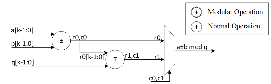
However, modular multiplication can be implemented using different techniques. The commonly used Barrett reduction and Montgomery reduction require additional multiplications and are more suitable for the non-specific modulus. Furthermore, Montgomery reduction needs two more steps to convert all inputs from normal domain to Montgomery domain and then convert back the results into normal domain. This conversation increases the latency of NTT operations and does not lead to the best performance. Hence, Barrett reduction and Montgomery reduction are expensive in time and hardware resources.
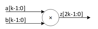
For Dilithium hardware accelerator, we can customize the reduction architecture based on the prime value of the scheme with q= 8,380,417 to design a hardware-friendly architecture that increase the efficiency of computation. The value of q can be presented by:
q=8,380,417=223-213+1
For the modular operation we have:
223=213-1 mod q
Suppose that all input operands are less than q, we have:
0≤a,b<q
z=a.b<q2=46'h3FE0_04FF_C001
Based on 223=213-1 mod q, we can rewrite the equation as follows:
z=223z45:23+z22:0=213z45:23-z45:23+z22:0=223z45:33+213z32:23-z45:23+z22:0=213z45:33-z45:33+213z32:23-z45:23+z22:0=223z45:43+213z42:33-z45:33+213z32:23-z45:23+z22:0=213z45:43-z45:43+213z42:33-z45:33+213z32:23-z45:23+z22:0=213z45:43+z42:33+z32:23+-z45:43-z45:33-z45:23+z22:0=213z45:43+z42:33+z32:23+z22:13+-z45:43-z45:33-z45:23+z12:0=213c-(z45:43+z45:33+z45:23)+z[12:0]
Where:
c=z45:43+z42:33+z32:23+z[22:13]<212
The value of c has 12 bits, and we can rewrite it as follows:
213c11:0=223c11:10+213c9:0=213c11:10-c11:10+213c9:0=213d-c11:10
d=c11:10+c9:0
So, the value of z mod q is as follows:
z=213c-z45:43+z45:33+z45:23+z12:0=213d+z12:0-z45:43+z45:33+z45:23+c11:10=213d+z12:0-e
Where:
e=z45:43+z45:33+z45:23+c11:10=f+z45:23 mod q
f[14:0]=z45:43+z45:33+c11:10
We use a modular addition for f+z45:23 to keep it less than q. This modular addition has one stage delay.
The addition between 213d and z12:0 can be implemented by concatenating since the first 13 bits of d are zero as follows:
g23:0=213d+z12:0=d10:0||z[12:0]
Since the result has more than 23 bits, we perform a modular addition to keep it less than q. For that, the regular modular addition will be replaced by the following architecture while c0=g23, r0=g[22:0]. In other words, c0=d10, r0[22:0]=d9:0||z[12:0]
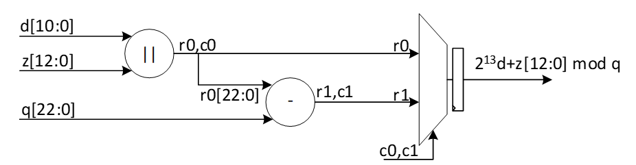
The following figure shows the architecture of this reduction technique. As one can see, these functions do not need any multiplications in hardware and can be achieved by shifter and adder.
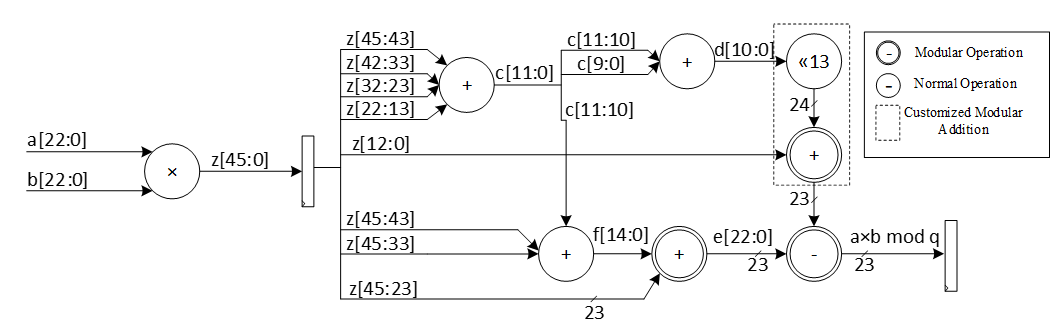
The modular multiplication is implemented with a 3-stage pipeline architecture. At the first pipeline stage, z=a·b is calculated. At the second pipeline stage, f+z[45:23] and 213d+z12:0 are calculated in parallel. At the third pipeline stage, a modular subtraction is executed to obtain the result and the result is output.
We do not need extra multiplications for our modular reduction, unlike Barrett and Montgomery algorithms. The operations of our reduction do not depend on the input data and do not leak any information. Our reduction using the modulus q= 8,380,417 is fast, efficient and constant-time.
Performance of NTT
For a complete NTT operation with 8 layers, i.e., n = 256, the proposed architecture takes 82=4 rounds. Each round involves 2564=64 operations in pipelined architecture. Hence, the latency of each round is equal to 64 (read from memory) + 8 (2 sequential butterfly latency) + 4 (input buffer latency) + 2 (wait between each two stages) = 78 cycles.
Round 0: stage 0 & 1
Round 1: stage 2 & 3
Round 2: stage 4 & 5
Round 3: stage 6 & 7
The total latency would be 4×78=312 cycles.
For a complete NTT/INTT operation for Dilithium ML-DSA-87 with 7 or 8 polynomials, 7*312=2184 or 8*312=2496 cycles are required. However, our design can be duplicated to enable parallel NTT for two different polynomials. Having two parallel design results in 1248 cycles.
NTT shuffling countermeasure
The Adams-Bridge NTT engine uses shuffling as one of two complementary side-channel countermeasures. Shuffling randomizes the per-coefficient execution order so that any observable side-channel emission cannot be correlated with a specific coefficient index. The reordering is purely a control-path permutation of the read/write address sequence, so it adds no datapath area and no latency overhead. Shuffling is available in all NTT operating modes (NTT, INTT, PWM, PWM-with-accumulation, PWA, PWS) and is gated by the shuffling_en field of the active opcode (see abr_ctrl_pkg.sv opcode definitions).
The shuffling random word is sourced from the top-level LFSR. When MASKING_EN = 1 two NTT engines are instantiated, and each engine receives an independent shuffling_rand slice from the LFSR so that NTT[0] and NTT[1] execute different permutations of the same logical operation. This prevents trace alignment across the two shares.
Shuffling is the only in-NTT countermeasure. The complementary arithmetic masking countermeasure (data-domain splitting into two arithmetic shares of each coefficient) is implemented at the architectural level, outside the NTT engine — see PWM and INTT masking countermeasure below.
The pre-shuffle in-order memory layout for one NTT polynomial (4 coefficients per address × 64 addresses = 256 coefficients) is shown in the table below; the shuffler permutes the read/write order over these same addresses.
| Address | Memory Content | ||||
|---|---|---|---|---|---|
| 0 | 0 | 1 | 2 | 3 | |
| 1 | 4 | 5 | 6 | 7 | |
| 2 | 8 | 9 | 10 | 11 | |
| 3 | 12 | 13 | 14 | 15 | |
| 4 | 16 | 17 | 18 | 19 | |
| 5 | 20 | 21 | 22 | 23 | |
| 6 | 24 | 25 | 26 | 27 | |
| 7 | 28 | 29 | 30 | 31 | |
| 8 | 32 | 33 | 34 | 35 | |
| 9 | 36 | 37 | 38 | 39 | |
| 10 | 40 | 41 | 42 | 43 | |
| 11 | 44 | 45 | 46 | 47 | |
| 12 | 48 | 49 | 50 | 51 | |
| 13 | 52 | 53 | 54 | 55 | |
| 14 | 56 | 57 | 58 | 59 | |
| 15 | 60 | 61 | 62 | 63 | |
| 16 | 64 | 65 | 66 | 67 | |
| 17 | 68 | 69 | 70 | 71 | |
| 18 | 72 | 73 | 74 | 75 | |
| 19 | 76 | 77 | 78 | 79 | |
| 20 | 80 | 81 | 82 | 83 | |
| 21 | 84 | 85 | 86 | 87 | |
| 22 | 88 | 89 | 90 | 91 | |
| 23 | 92 | 93 | 94 | 95 | |
| 24 | 96 | 97 | 98 | 99 | |
| 25 | 100 | 101 | 102 | 103 | |
| 26 | 104 | 105 | 106 | 107 | |
| 27 | 108 | 109 | 110 | 111 | |
| 28 | 112 | 113 | 114 | 115 | |
| 29 | 116 | 117 | 118 | 119 | |
| 30 | 120 | 121 | 122 | 123 | |
| 31 | 124 | 125 | 126 | 127 | |
| 32 | 128 | 129 | 130 | 131 | |
| 33 | 132 | 133 | 134 | 135 | |
| 34 | 136 | 137 | 138 | 139 | |
| 35 | 140 | 141 | 142 | 143 | |
| 36 | 144 | 145 | 146 | 147 | |
| 37 | 148 | 149 | 150 | 151 | |
| 38 | 152 | 153 | 154 | 155 | |
| 39 | 156 | 157 | 158 | 159 | |
| 40 | 160 | 161 | 162 | 163 | |
| 41 | 164 | 165 | 166 | 167 | |
| 42 | 168 | 169 | 170 | 171 | |
| 43 | 172 | 173 | 174 | 175 | |
| 44 | 176 | 177 | 178 | 179 | |
| 45 | 180 | 181 | 182 | 183 | |
| 46 | 184 | 185 | 186 | 187 | |
| 47 | 188 | 189 | 190 | 191 | |
| 48 | 192 | 193 | 194 | 195 | |
| 49 | 196 | 197 | 198 | 199 | |
| 50 | 200 | 201 | 202 | 203 | |
| 51 | 204 | 205 | 206 | 207 | |
| 52 | 208 | 209 | 210 | 211 | |
| 53 | 212 | 213 | 214 | 215 | |
| 54 | 216 | 217 | 218 | 219 | |
| 55 | 220 | 221 | 222 | 223 | |
| 56 | 224 | 225 | 226 | 227 | |
| 57 | 228 | 229 | 230 | 231 | |
| 58 | 232 | 233 | 234 | 235 | |
| 59 | 236 | 237 | 238 | 239 | |
| 60 | 240 | 241 | 242 | 243 | |
| 61 | 244 | 245 | 246 | 247 | |
| 62 | 248 | 249 | 250 | 251 | |
| 63 | 252 | 253 | 254 | 255 |
To implement shuffling in NTT, the memory content is divided into 16 chunks. The highlighted section in the memory table above shows the 16 chunk start addresses. For example, the first chunk consists of addresses 0, 16, 32, 48. Second chunk has 1, 17, 33, 49, and so on. In NTT mode, memory read pattern is 0, 16, 32, 48, 1, 17, 33, 49, etc. The buffer in NTT module is updated to have two sections and is addressable to support INTT shuffling with matched search space as that of NTT mode.
During shuffling, two levels of randomization are done:
- Chunk order is randomized
- Start address within the selected chunk is also randomized.
With this technique, the search space is 16 ×416=236. For example, if chunk 5 is selected as the starting chunk, the input buffer in NTT mode is configured as below.
| 2151 | 2140 | 2133 | 2122 |
| 1511 | 1500 | 1493 | 1482 |
| 871 | 860 | 853 | 842 |
| 231 | 220 | 213 | 202 |
Then, the order of execution is randomized for NTT as a second level of randomization. For example, order of execution in NTT mode can be (22, 86, 150, 214), (23, 87, 151, 215), (20, 84, 148, 212), (21, 85, 149, 213). Note that, once a random start address is selected, the addresses increment from that point and wrap around until all 4 sets of coefficients have been processed in order. Similarly, once a random chunk is selected, rest of the chunks are processed in order and wrapped around until all chunks are covered. In this example, chunk processing order is 5, 6, 7, 8, …, 15, 0, 1, 2, 3, 4.
For the next chunk, buffer pointer switches to the top half. While the bottom half of the buffer is read and executed, each location of the top half is filled in the same cycle avoiding latency overhead. When all 4 entries of the lower buffer are processed, upper buffer is ready to be fed into BF units.
| 2193 | 2183 | 2173 | 2163 |
|---|---|---|---|
| 1552 | 1542 | 1532 | 1522 |
| 911 | 901 | 891 | 881 |
| 270 | 260 | 250 | 240 |
| 2151 | 2140 | 2133 | 2122 |
| 1511 | 1500 | 1493 | 1482 |
| 871 | 860 | 853 | 842 |
| 231 | 220 | 213 | 202 |
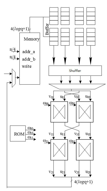
Above figure shows the flow of a shuffled NTT/INTT operation. The shuffler part of the controller is responsible for calculating the correct memory addresses and feed the correct inputs to the BFs.
When shuffling in NTT mode, the memory read and write addresses are computed as shown below.for i in range (0, 4):
Read address \= chunk \+ (i \* RD\_STEP)
Write address = chunk * 4 + (rand_index * WR_STEP)
Where rand_index is the randomized start index of execution order for an NTT operation
E.g. if selected chunk is 5, and rand_index is 2
Order of execution is 2, 3, 0, 1

Read address \= 5 \+ (0\*16), 5 \+ (1\*16), 5+(2\*16), 5+(3\*16) \= 5, 21, 37, 53

Write address \= (5\*4) \+ (2\*1), (5\*4) \+ (3\*1), (5\*4) \+ (0\*1), (5\*4) \+ (1\*1) \= 22, 23, 20, 21
Figure below shows the additional control logic required to maintain the shuffling mechanism.
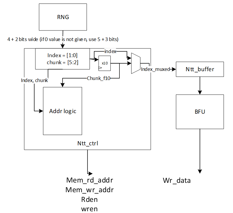
The index and chunk are obtained from a random number source. Chunk refers to starting chunk number and index refers to start address within the selected chunk. To account for BF latency, the index and chunk must be delayed appropriately (for our design, this latency is 10 cycles) for use in the controller shuffler logic.
The general address calculation for NTT is:
mem read addr=chunk+(countregular*STEPrd)
Since reading memory can be in order, a regular counter is used to read all 4 addresses of the selected chunk.
mem write addr=chunkf10*4+indexf10*STEPwr
The buffer address calculation for NTT is:
buffer write addr=countregular
buffer read addr=countindex
Where f10 refers to delayed values by 10 cycles. In this logic, chunk is updated every 4 cycles and buffer pointer is toggled (to top or bottom half) every 4 cycles.
The general address calculation for INTT is:
mem read addr=(chunk*4)+(index*STEPrd)
mem write addr=chunkf10+countregular*STEPwr
Since writing to memory can be in order, a regular counter is used to write all 4 addresses of the selected chunk.
In INTT, index need not be delayed since the BFs consume the coefficients in the next cycle.
The buffer address calculation for INTT is:
buffer write addr=indexf10
buffer read addr=countregular
Rejection Sampler architecture
Dilithium (or Kyber) samples the polynomials that make up the vectors and matrices independently, using a fixed seed value and a nonce value that increases the security as the input for Keccak. Keccak is used to take these seed and nonce and generate random stream bits.
Rejection sampler takes 24-bits (12 bits in case of Kyber) and checks if it is less than the prime number q = 223 −213+1 = 8380417 (q=3369 in case of Kyber). It continues to sample all required coefficients, n=256, for a polynomial.
After sampling a polynomial with 256 coefficients, nonce will be changed and a new random stream will be generated using Keccak core and will be sampled by rejection sampling unit.
The output of this operation results in a matrix of polynomial with k rows and l column while each polynomial includes 256 coefficients.
\[ \begin{bmatrix} A_{0,0} & \cdots & A_{0,l-1} \ \vdots & \ddots & \vdots \ A_{k-1,0} & \cdots & A_{k-1,l-1} \end{bmatrix} _{k*l} \] Rejection sampling is used in all three operations of Dilithium, i.e., keygen, sign, and verify. Since based on the specification of the Dilithium (and Kyber), the sampled coefficients are considered in NTT domain, the output of rejection sampler can directly be used for polynomial multiplication operation, as follows:
\[ \begin{bmatrix} A_{0,0} & \cdots & A_{0,l-1} \ \vdots & \ddots & \vdots \ A_{k-1,0} & \cdots & A_{k-1,l-1} \end{bmatrix} \circ \begin{bmatrix} s_{1,0} \ \vdots \ s_{1,l-1} \end
\begin{bmatrix} A_{0,0} \circ s_{1,0} + \cdots + A_{0,l-1} \circ s_{1,l-1} \ \vdots \ A_{k-1,0} \circ s_{1,0} + \cdots + A_{k-1,l-1} \circ s_{1,l-1} \end{bmatrix} \]
We propose an architecture to remove the cost of memory access from Keccak to rejection sampler, and from rejection sampler to polynomial multiplier. To achieve this, we need to have a balanced throughput between all these modules to avoid large buffering or conflict between them.
High-level architecture is illustrated as follows:
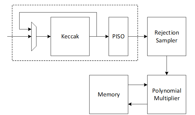
Keccak interface to Rejection Sampler
Keccak is used in SHAKE-128 configuration for rejection sampling operation. Hence, it will take the input data and generates 1344-bit output after each round. We propose implementing of Keccak while each round takes 12 cycles. The format of input data is as follows:
Input data = ρ | j | i
Where is seed with 256-bits, i and j are nonce that describes the row and column number of corresponding polynomial A such that:
Ai,j=Rejection_sampling(Keccak(ρ | j | i))
Since each 24-bit is used for one coefficient, each round of Keccak output provides 1344/24=56 coefficients. To have 256 coefficients for each polynomial (with same seed and nonce), we need to rerun Keccak for at least 5 rounds.
There are two paths for Keccak input. While the input can be set by controller for each new polynomial, the loop path is used to rerun Keccak for completing the previous polynomial.
Rejection sampler cannot take all 1344-bit output parallelly since it makes hardware architecture too costly and complex, and also there is no other input from Keccak for the next 12 cycles. Therefore, we propose a parallel-input serial-output (PISO) unit in between to store the Keccak output and feed rejection unit sequentially.
Rejection Sampler
This unit takes data from the output of SHAKE-128 stored in a PISO buffer. The required cycles for this unit are variable due to the non-deterministic pattern of rejection sampling. However, at least 5 Keccak rounds are required to provide 256 coefficients.
In our optimized architecture, this unit works in parallel with the Keccak core. Therefore, the latency for rejection sampling is absorbed within the latency for a concurrently running Keccak core.
Our proposed polynomial multiplier can perform point-wise multiplication on four coefficients per cycle that also helps to avoid memory access challenges and make the control logic too complicated. This implies that the optimal speed of the rejection sampling module is to sample four coefficients without rejection in one cycle.
On the output side, as the rejection sampling might fail, the rejection rate for each input is:
\[rejection_rate= 1-q/2^23=1-8380471/2^23=0.0009764≈10^{-3}\]
Hence, the probability of failure to provide 4 appropriate coefficients from 4 inputs would be:
\[1-(1-rejection_rate)^4=0.00399\]
To reduce the failure probability and avoid any wait cycle in polynomial multiplication, 5 coefficients are fed into rejection while only 4 of them will be passed to polynomial multiplication. This decision reduces the probability of failure to
\[ 1 - (\text{probability of having 5 good inputs}) - (\text{probability of having 4 good inputs}) = 1 - (1 - \text{rejection_rate})^5 - \text{rejection_rate} \cdot \binom{5}{4} \cdot (1 - \text{rejection_rate})^4 = 0.00000998≈10^{-5} \]
Adding a FIFO to rejection sampling unit can store the remaining unused coefficients and increase the probability of having 4 appropriate coefficients to match polynomial multiplication throughput. The architecture is as follows:
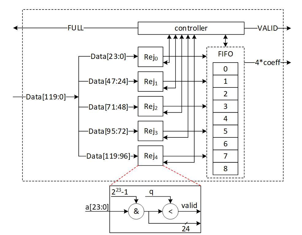
There are 5 rejection sampler circuits corresponding to each 24-bit input. The controller checks if each of these coefficients should be rejected or not. The valid input coefficients can be stored into the FIFO. While maximum 5 coefficients can be fed into FIFO, there are four more entries for the remaining coefficients from the previous cycle. There are several scenarios for the proposed balanced throughput architecture:
- At the very first cycle, or whenever the FIFO is empty, rejection sampling unit may not provide all 4 coefficients for polynomial multiplication unit. We reduce the failure probability of this scenario by feeding 5 coefficients, however, it may happen. So, for designing efficient architecture, instead of reducing the failure probability by adding more hardware cost, we use a VALID output that stops polynomial multiplier until all 4 required coefficients are sampled.
- If all 5 inputs are valid, they are going to be stored into FIFO. The first 4 coefficients will be sent to polynomial multiplication unit, while the remaining coefficients will be shifted to head of FIFO and be used for the next cycle with the first 3 valid coefficients from the next cycle.
- The maximum depth of FIFO is 9 entries. If all 9 FIFO entries are full, rejection sampling unit can provide the required output for the next cycles too. Hence, it does not accept a new input from Keccak core by raising FULL flag.
| Cycle count | Input from PISO | FIFO valid entries from previous cycle | Total valid samples | output | FIFO remaining for the next cycle |
|---|---|---|---|---|---|
| 0 | 5 | 0 | 5 | 4 | 1 |
| 1 | 5 | 1 | 6 | 4 | 2 |
| 2 | 5 | 2 | 7 | 4 | 3 |
| 3 | 5 | 3 | 8 | 4 | 4 |
| 4 | 5 | 4 | 9 | 4 | 5 (FULL) |
| 5 | 0 | 5 | 5 | 4 | 1 |
| 6 | 5 | 1 | 6 | 4 | 2 |
- If there is not FULL condition for reading from Keccak, all PISO data can be read in 12 cycles, including 11 cycles with 5 coefficients and 1 cycle for the 56th coefficient. This would be match with Keccak throughput that generates 56 coefficients per 12 cycles.
- The maximum number of FULL conditions is when there are no rejected coefficients for all 56 inputs. In this case, after 5 cycles with 5 coefficients, there is one FULL condition. After 12 cycles, 50 coefficients are processed by rejection sampling unit, and there are still 6 coefficients inside PISO. To maximize the utilization factor of our hardware resources, Keccak core will check the PISO status. If PISO contains 5 coefficients or more (the required inputs for rejection sampling unit), EMPTY flag will not be set, and Keccak will wait until the next cycle. Hence, rejection sampling unit takes 13 cycles to process 55 coefficients, and the last coefficients will be combined with the next Keccak round to be processed.
Performance of SampleRejq
For processing each round of Keccak using rejection sampling unit, we need 12 to 13 cycles that result in 60-65 cycles for each polynomial with 256 coefficients.
For a complete rejection sampling for Dilithium ML-DSA-87 with 8*7=56 polynomials, 3360 to 3640 cycles are required using sequential operation. However, our design can be duplicated to enable parallel sampling for two different polynomials. Having two parallel design results in 1680 to 1820 cycles, while three parallel design results in 1120 to 1214 cycles at the cost of more resource utilization.
INTT architecture
A merged-layer INTT technique uses two pipelined stages with two parallel cores in each stage level, making 4 butterfly cores in total. The parallel pipelined butterfly cores enable us to perform Radix-4 INTT operation with 4 parallel coefficients.
However, INTT requires a specific memory pattern that may limit the efficiency of the butterfly operation. For Dilithium use case, there are n=256 coefficients per polynomial that requires log n=8 layers of INTT operations. Each butterfly unit takes two coefficients while difference between the indexes is 2i-1 in ith stage. That means for the first stage, the given indexes for each butterfly unit are (2*k, 2*k+1):
Stage 1 input indexes: {(0, 1), {2, 3), (4, 5), …, (254, 255)}
Stage 2 input indexes: {(0, 2), {1, 3), (4, 6), …, (61, 63), (64, 66), (65, 67), …, (253, 255)}
…
Stage 8 input indexes: {(0, 128), {1, 129), (2, 130), …, (127, 255)}
There are several considerations for that:
- We need access to 4 coefficients per cycle to match the throughput into 2×2 butterfly units.
- An optimized architecture provides a memory with only one reading port, and one writing port.
- Based on the previous two notes, each memory address contains 4 coefficients.
- The initial coefficients are stored sequentially by NTT. Specifically, they begin with 0 and continue incrementally up to 255. Hence, at the very beginning cycle, the memory contains (0, 1, 2, 3) in the first address, (4, 5, 6, 7) in second address, and so on.
- The cost of in-place memory relocation to align the memory content is not negligible. Particularly, it needs to be repeated for each stage.
While memory bandwidth limits the efficiency of the butterfly operation, we use a specific memory pattern to store four coefficients per address.
We propose a pipeline architecture the read memory in a particular pattern and using a set of buffers, the corresponding coefficients are fed into INTT block.
The initial memory contains the indexes as follows:
| Address | Initial Memory Content | |||
|---|---|---|---|---|
| 0 | 0 | 1 | 2 | 3 |
| 1 | 4 | 5 | 6 | 7 |
| 2 | 8 | 9 | 10 | 11 |
| 3 | 12 | 13 | 14 | 15 |
| 4 | 16 | 17 | 18 | 19 |
| 5 | 20 | 21 | 22 | 23 |
| 6 | 24 | 25 | 26 | 27 |
| 7 | 28 | 29 | 30 | 31 |
| 8 | 32 | 33 | 34 | 35 |
| 9 | 36 | 37 | 38 | 39 |
| 10 | 40 | 41 | 42 | 43 |
| 11 | 44 | 45 | 46 | 47 |
| 12 | 48 | 49 | 50 | 51 |
| 13 | 52 | 53 | 54 | 55 |
| 14 | 56 | 57 | 58 | 59 |
| 15 | 60 | 61 | 62 | 63 |
| 16 | 64 | 65 | 66 | 67 |
| 17 | 68 | 69 | 70 | 71 |
| 18 | 72 | 73 | 74 | 75 |
| 19 | 76 | 77 | 78 | 79 |
| 20 | 80 | 81 | 82 | 83 |
| 21 | 84 | 85 | 86 | 87 |
| 22 | 88 | 89 | 90 | 91 |
| 23 | 92 | 93 | 94 | 95 |
| 24 | 96 | 97 | 98 | 99 |
| 25 | 100 | 101 | 102 | 103 |
| 26 | 104 | 105 | 106 | 107 |
| 27 | 108 | 109 | 110 | 111 |
| 28 | 112 | 113 | 114 | 115 |
| 29 | 116 | 117 | 118 | 119 |
| 30 | 120 | 121 | 122 | 123 |
| 31 | 124 | 125 | 126 | 127 |
| 32 | 128 | 129 | 130 | 131 |
| 33 | 132 | 133 | 134 | 135 |
| 34 | 136 | 137 | 138 | 139 |
| 35 | 140 | 141 | 142 | 143 |
| 36 | 144 | 145 | 146 | 147 |
| 37 | 148 | 149 | 150 | 151 |
| 38 | 152 | 153 | 154 | 155 |
| 39 | 156 | 157 | 158 | 159 |
| 40 | 160 | 161 | 162 | 163 |
| 41 | 164 | 165 | 166 | 167 |
| 42 | 168 | 169 | 170 | 171 |
| 43 | 172 | 173 | 174 | 175 |
| 44 | 176 | 177 | 178 | 179 |
| 45 | 180 | 181 | 182 | 183 |
| 46 | 184 | 185 | 186 | 187 |
| 47 | 188 | 189 | 190 | 191 |
| 48 | 192 | 193 | 194 | 195 |
| 49 | 196 | 197 | 198 | 199 |
| 50 | 200 | 201 | 202 | 203 |
| 51 | 204 | 205 | 206 | 207 |
| 52 | 208 | 209 | 210 | 211 |
| 53 | 212 | 213 | 214 | 215 |
| 54 | 216 | 217 | 218 | 219 |
| 55 | 220 | 221 | 222 | 223 |
| 56 | 224 | 225 | 226 | 227 |
| 57 | 228 | 229 | 230 | 231 |
| 58 | 232 | 233 | 234 | 235 |
| 59 | 236 | 237 | 238 | 239 |
| 60 | 240 | 241 | 242 | 243 |
| 61 | 244 | 245 | 246 | 247 |
| 62 | 248 | 249 | 250 | 251 |
| 63 | 252 | 253 | 254 | 255 |
Suppose memory is read in the regular pattern:
Reading Addr: 0, 1, 2, 3, 4, …, 62, 63
The input goes to the butterfly architecture. The input values contain the required coefficients for our butterfly units in the next stage, i.e., (0, 1) and (2, 3). Since we merged the first and second layers of INTT stages, the output of the first parallel butterfly units need to exchange one coefficient and then the required input for the second parallel set of butterfly units is ready, i.e., (0, 2) and (1, 3).
To prepare the results for the next stages, the output needs to be stored into the customized buffer architecture as follows:
| 0 | → | |||||||
|---|---|---|---|---|---|---|---|---|
| 1 | ||||||||
| 2 | ||||||||
| 3 |
Cycle 0 after butterfly reading address 0
| 4 | → | 0 | ||||||
|---|---|---|---|---|---|---|---|---|
| 5 | 1 | |||||||
| 6 | 2 | |||||||
| 7 | 3 |
Cycle 0 after butterfly reading address 1
| 8 | → | 4 | 0 | |||||
|---|---|---|---|---|---|---|---|---|
| 9 | 5 | 1 | ||||||
| 10 | 6 | 2 | ||||||
| 11 | 7 | 3 |
Cycle 2 after butterfly reading address 2
| 12 | → | 8 | 4 | 0 | ||||
|---|---|---|---|---|---|---|---|---|
| 13 | 9 | 5 | 1 | |||||
| 14 | 10 | 6 | 2 | |||||
| 15 | 11 | 7 | 3 |
Cycle 3 after butterfly reading address 3
| 16 | → | 12 | 8 | 4 | 0 | |||
|---|---|---|---|---|---|---|---|---|
| 17 | 13 | 9 | 5 | 1 | ||||
| 18 | 14 | 10 | 6 | 2 | ||||
| 19 | 15 | 11 | 7 | 3 |
Cycle 4 after butterfly reading address 4
| 20 | → | 16 | 12 | 8 | 4 | |||
|---|---|---|---|---|---|---|---|---|
| 21 | 17 | 13 | 9 | 5 | 1 | |||
| 22 | 18 | 14 | 10 | 6 | 2 | |||
| 23 | 19 | 15 | 11 | 7 | 3 |
Cycle 5 after butterfly reading address 5
The highlighted value in the first buffer contains the required coefficients for our butterfly units in the next stage, i.e., (0, 4) and (8, 12).
However, we need to write the output in a particular pattern as follows:
Writing Addr: 0, 16, 32, 48, 1, 17, 33, 49, …, 15, 31, 47, 63
After completing the first round of operation including INTT stage 1 and 2, the memory contains the following data:
| Address | Memory Content after 1&2 stages | |||
|---|---|---|---|---|
| 0 | 0 | 4 | 8 | 12 |
| 1 | 16 | 20 | 24 | 28 |
| 2 | 32 | 36 | 40 | 44 |
| 3 | 48 | 52 | 56 | 60 |
| 4 | 64 | 68 | 72 | 76 |
| 5 | 80 | 84 | 88 | 92 |
| 6 | 96 | 100 | 104 | 108 |
| 7 | 112 | 116 | 120 | 124 |
| 8 | 128 | 132 | 136 | 140 |
| 9 | 144 | 148 | 152 | 156 |
| 10 | 160 | 164 | 168 | 172 |
| 11 | 176 | 180 | 184 | 188 |
| 12 | 192 | 196 | 200 | 204 |
| 13 | 208 | 212 | 216 | 220 |
| 14 | 224 | 228 | 232 | 236 |
| 15 | 240 | 244 | 248 | 252 |
| 16 | 1 | 5 | 9 | 13 |
| 17 | 17 | 21 | 25 | 29 |
| 18 | 33 | 37 | 41 | 45 |
| 19 | 49 | 53 | 57 | 61 |
| 20 | 65 | 69 | 73 | 77 |
| 21 | 81 | 85 | 89 | 93 |
| 22 | 97 | 101 | 105 | 109 |
| 23 | 113 | 117 | 121 | 125 |
| 24 | 129 | 133 | 137 | 141 |
| 25 | 145 | 149 | 153 | 157 |
| 26 | 161 | 165 | 169 | 173 |
| 27 | 177 | 181 | 185 | 189 |
| 28 | 193 | 197 | 201 | 205 |
| 29 | 209 | 213 | 217 | 221 |
| 30 | 225 | 229 | 233 | 237 |
| 31 | 241 | 245 | 249 | 253 |
| 32 | 2 | 6 | 10 | 14 |
| 33 | 18 | 22 | 26 | 30 |
| 34 | 34 | 38 | 42 | 46 |
| 35 | 50 | 54 | 58 | 62 |
| 36 | 66 | 70 | 74 | 78 |
| 37 | 82 | 86 | 90 | 94 |
| 38 | 98 | 102 | 106 | 110 |
| 39 | 114 | 118 | 122 | 126 |
| 40 | 130 | 134 | 138 | 142 |
| 41 | 146 | 150 | 154 | 158 |
| 42 | 162 | 166 | 170 | 174 |
| 43 | 178 | 182 | 186 | 190 |
| 44 | 194 | 198 | 202 | 206 |
| 45 | 210 | 214 | 218 | 222 |
| 46 | 226 | 230 | 234 | 238 |
| 47 | 242 | 246 | 250 | 254 |
| 48 | 3 | 7 | 11 | 15 |
| 49 | 19 | 23 | 27 | 31 |
| 50 | 35 | 39 | 43 | 47 |
| 51 | 51 | 55 | 59 | 63 |
| 52 | 67 | 71 | 75 | 79 |
| 53 | 83 | 87 | 91 | 95 |
| 54 | 99 | 103 | 107 | 111 |
| 55 | 115 | 119 | 123 | 127 |
| 56 | 131 | 135 | 139 | 143 |
| 57 | 147 | 151 | 155 | 159 |
| 58 | 163 | 167 | 171 | 175 |
| 59 | 179 | 183 | 187 | 191 |
| 60 | 195 | 199 | 203 | 207 |
| 61 | 211 | 215 | 219 | 223 |
| 62 | 227 | 231 | 235 | 239 |
| 63 | 243 | 247 | 251 | 255 |
The same process can be applied in the next round to perform INTT stage 3 and 4.
| 0 | → | |||||||
|---|---|---|---|---|---|---|---|---|
| 4 | ||||||||
| 8 | ||||||||
| 12 |
Cycle 0 after butterfly reading address 0
| 16 | → | 0 | ||||||
|---|---|---|---|---|---|---|---|---|
| 20 | 4 | |||||||
| 24 | 8 | |||||||
| 28 | 12 |
Cycle 1 after butterfly reading address 1
| 32 | → | 16 | 0 | |||||
|---|---|---|---|---|---|---|---|---|
| 36 | 20 | 4 | ||||||
| 40 | 24 | 8 | ||||||
| 44 | 28 | 12 |
Cycle 2 after butterfly reading address 2
| 48 | → | 32 | 16 | 0 | ||||
|---|---|---|---|---|---|---|---|---|
| 52 | 36 | 20 | 4 | |||||
| 56 | 40 | 24 | 8 | |||||
| 60 | 44 | 28 | 12 |
Cycle 3 after butterfly reading address 3
| 64 | → | 48 | 32 | 16 | 0 | |||
|---|---|---|---|---|---|---|---|---|
| 68 | 52 | 36 | 20 | 4 | ||||
| 72 | 56 | 40 | 24 | 8 | ||||
| 76 | 60 | 44 | 28 | 12 |
Cycle 4 after butterfly reading address 4
| 80 | → | 64 | 48 | 32 | 16 | |||
|---|---|---|---|---|---|---|---|---|
| 84 | 68 | 52 | 36 | 20 | 4 | |||
| 88 | 72 | 56 | 40 | 24 | 8 | |||
| 92 | 76 | 60 | 44 | 28 | 12 |
Cycle 5 after butterfly reading address 5
After completing all stages, the memory contents would be as follows:
| Address | Memory Content after Stage 7&8 | |||
|---|---|---|---|---|
| 0 | 0 | 1 | 2 | 3 |
| 1 | 4 | 5 | 6 | 7 |
| 2 | 8 | 9 | 10 | 11 |
| 3 | 12 | 13 | 14 | 15 |
| 4 | 16 | 17 | 18 | 19 |
| 5 | 20 | 21 | 22 | 23 |
| 6 | 24 | 25 | 26 | 27 |
| 7 | 28 | 29 | 30 | 31 |
| 8 | 32 | 33 | 34 | 35 |
| 9 | 36 | 37 | 38 | 39 |
| 10 | 40 | 41 | 42 | 43 |
| 11 | 44 | 45 | 46 | 47 |
| 12 | 48 | 49 | 50 | 51 |
| 13 | 52 | 53 | 54 | 55 |
| 14 | 56 | 57 | 58 | 59 |
| 15 | 60 | 61 | 62 | 63 |
| 16 | 64 | 65 | 66 | 67 |
| 17 | 68 | 69 | 70 | 71 |
| 18 | 72 | 73 | 74 | 75 |
| 19 | 76 | 77 | 78 | 79 |
| 20 | 80 | 81 | 82 | 83 |
| 21 | 84 | 85 | 86 | 87 |
| 22 | 88 | 89 | 90 | 91 |
| 23 | 92 | 93 | 94 | 95 |
| 24 | 96 | 97 | 98 | 99 |
| 25 | 100 | 101 | 102 | 103 |
| 26 | 104 | 105 | 106 | 107 |
| 27 | 108 | 109 | 110 | 111 |
| 28 | 112 | 113 | 114 | 115 |
| 29 | 116 | 117 | 118 | 119 |
| 30 | 120 | 121 | 122 | 123 |
| 31 | 124 | 125 | 126 | 127 |
| 32 | 128 | 129 | 130 | 131 |
| 33 | 132 | 133 | 134 | 135 |
| 34 | 136 | 137 | 138 | 139 |
| 35 | 140 | 141 | 142 | 143 |
| 36 | 144 | 145 | 146 | 147 |
| 37 | 148 | 149 | 150 | 151 |
| 38 | 152 | 153 | 154 | 155 |
| 39 | 156 | 157 | 158 | 159 |
| 40 | 160 | 161 | 162 | 163 |
| 41 | 164 | 165 | 166 | 167 |
| 42 | 168 | 169 | 170 | 171 |
| 43 | 172 | 173 | 174 | 175 |
| 44 | 176 | 177 | 178 | 179 |
| 45 | 180 | 181 | 182 | 183 |
| 46 | 184 | 185 | 186 | 187 |
| 47 | 188 | 189 | 190 | 191 |
| 48 | 192 | 193 | 194 | 195 |
| 49 | 196 | 197 | 198 | 199 |
| 50 | 200 | 201 | 202 | 203 |
| 51 | 204 | 205 | 206 | 207 |
| 52 | 208 | 209 | 210 | 211 |
| 53 | 212 | 213 | 214 | 215 |
| 54 | 216 | 217 | 218 | 219 |
| 55 | 220 | 221 | 222 | 223 |
| 56 | 224 | 225 | 226 | 227 |
| 57 | 228 | 229 | 230 | 231 |
| 58 | 232 | 233 | 234 | 235 |
| 59 | 236 | 237 | 238 | 239 |
| 60 | 240 | 241 | 242 | 243 |
| 61 | 244 | 245 | 246 | 247 |
| 62 | 248 | 249 | 250 | 251 |
| 63 | 252 | 253 | 254 | 255 |
The proposed method saves the time needed for shuffling and reordering, while using only a little more memory.
INTT shuffling countermeasure
Similar to NTT operation, INTT requires shuffling the order of execution of coefficients in order to mitigate SCA attacks. Refer to section 5.3.3 for details on NTT shuffling. In INTT mode, the chunks are split in the following pattern into 16 chunks:
| Address | 1&2 | ||||
|---|---|---|---|---|---|
| 0 | 0 | 1 | 2 | 3 | |
| 1 | 4 | 5 | 6 | 7 | |
| 2 | 8 | 9 | 10 | 11 | |
| 3 | 12 | 13 | 14 | 15 | |
| 4 | 16 | 17 | 18 | 19 | |
| 5 | 20 | 21 | 22 | 23 | |
| 6 | 24 | 25 | 26 | 27 | |
| 7 | 28 | 29 | 30 | 31 | |
| 8 | 32 | 33 | 34 | 35 | |
| 9 | 36 | 37 | 38 | 39 | |
| 10 | 40 | 41 | 42 | 43 | |
| 11 | 44 | 45 | 46 | 47 | |
| 12 | 48 | 49 | 50 | 51 | |
| 13 | 52 | 53 | 54 | 55 | |
| 14 | 56 | 57 | 58 | 59 | |
| 15 | 60 | 61 | 62 | 63 | |
| 16 | 64 | 65 | 66 | 67 | |
| 17 | 68 | 69 | 70 | 71 | |
| 18 | 72 | 73 | 74 | 75 | |
| 19 | 76 | 77 | 78 | 79 | |
| 20 | 80 | 81 | 82 | 83 | |
| 21 | 84 | 85 | 86 | 87 | |
| 22 | 88 | 89 | 90 | 91 | |
| 23 | 92 | 93 | 94 | 95 | |
| 24 | 96 | 97 | 98 | 99 | |
| 25 | 100 | 101 | 102 | 103 | |
| 26 | 104 | 105 | 106 | 107 | |
| 27 | 108 | 109 | 110 | 111 | |
| 28 | 112 | 113 | 114 | 115 | |
| 29 | 116 | 117 | 118 | 119 | |
| 30 | 120 | 121 | 122 | 123 | |
| 31 | 124 | 125 | 126 | 127 | |
| 32 | 128 | 129 | 130 | 131 | |
| 33 | 132 | 133 | 134 | 135 | |
| 34 | 136 | 137 | 138 | 139 | |
| 35 | 140 | 141 | 142 | 143 | |
| 36 | 144 | 145 | 146 | 147 | |
| 37 | 148 | 149 | 150 | 151 | |
| 38 | 152 | 153 | 154 | 155 | |
| 39 | 156 | 157 | 158 | 159 | |
| 40 | 160 | 161 | 162 | 163 | |
| 41 | 164 | 165 | 166 | 167 | |
| 42 | 168 | 169 | 170 | 171 | |
| 43 | 172 | 173 | 174 | 175 | |
| 44 | 176 | 177 | 178 | 179 | |
| 45 | 180 | 181 | 182 | 183 | |
| 46 | 184 | 185 | 186 | 187 | |
| 47 | 188 | 189 | 190 | 191 | |
| 48 | 192 | 193 | 194 | 195 | |
| 49 | 196 | 197 | 198 | 199 | |
| 50 | 200 | 201 | 202 | 203 | |
| 51 | 204 | 205 | 206 | 207 | |
| 52 | 208 | 209 | 210 | 211 | |
| 53 | 212 | 213 | 214 | 215 | |
| 54 | 216 | 217 | 218 | 219 | |
| 55 | 220 | 221 | 222 | 223 | |
| 56 | 224 | 225 | 226 | 227 | |
| 57 | 228 | 229 | 230 | 231 | |
| 58 | 232 | 233 | 234 | 235 | |
| 59 | 236 | 237 | 238 | 239 | |
| 60 | 240 | 241 | 242 | 243 | |
| 61 | 244 | 245 | 246 | 247 | |
| 62 | 248 | 249 | 250 | 251 | |
| 63 | 252 | 253 | 254 | 255 |
(0, 1, 2, 3) addresses are chunk0, (4,5,6,7) are chunk1, etc. Chunk addresses are in order since for INTT, reads are in order and writes are out of order. Similar to NTT, two levels of randomization are used:
- Starting chunk is randomized
- Start address within each chunk is randomized
With this technique, the search space is 16 ×416=236. For example, if chunk 5 is selected as the starting chunk, and start address is 1, the order of execution is (21, 22, 23, 20). When next chunk is selected (chunk 6), start address is again randomized. For example, next order can be (27, 24, 25, 26) and so on.
The output buffer in INTT mode is configured as below. The buffer write pointer is aligned with the start address of the selected chunk and wraps around. In the given example, buffer write pointer increments as (1, 2, 3, 0) and the outputs of butterfly2x2 are stored in the buffer in locations (1, 2, 3, 0) in the order shown by superscript in the table below. This ensures the correct data is written back to memory to the correct addresses. In INTT mode, memory reads are randomized and memory writes will be in order.
| 1110 | 1100 | 1090 | 1080 |
|---|---|---|---|
| 1073 | 1063 | 1053 | 1043 |
| 1032 | 1022 | 1012 | 1002 |
| 991 | 981 | 971 | 961 |
| 952 | 942 | 932 | 922 |
| 911 | 901 | 891 | 881 |
| 870 | 860 | 850 | 840 |
| 833 | 823 | 813 | 803 |
While the next chunk starts, the data in the bottom half of the buffer is written to memory. Since every cycle there is a write to memory and write to the other half of the buffer, this incurs no latency overhead.
Memory read and write addresses are calculated as shown
for i in range (0, 4):
Read address \= (chunk\*4) \+ (rand\_index \* INTT\_RD\_STEP)
Write address = chunk + (i * INTT_WR_STEP)
Where rand_index is the randomized start index of execution order for an NTT operation
E.g. if selected chunk is 5, and rand_index is 2
Order of execution is 2, 3, 0, 1

Read address \= 5\*4 \+ (2\*1), 5\*4 \+ (3\*1), 5\*4+(0\*1), 5\*4+(1\*1) \= 22, 23, 20, 21

Write address \= 5 \+ (2\*16), 5 \+ (3\*16), 5 \+ (0\*16), 5 \+ (1\*16) \= 37, 53, 5, 21
Point-wise Multiplication architecture
Polynomial in NTT domain can be performed using point-wise multiplication (PWM). Considering the current architecture with 4 butterfly units, there are 4 modular multiplications that can be reused in point-wise multiplication operation. This approach enhances the design from an optimization perspective by resource sharing technique. `
There are 2 memories containing polynomial f and g, with 4 coefficients per each memory address. The parallel butterfly cores enable us to perform 4 point-wise multiplication operations with 4 parallel coefficients as follows:
The proposed NTT method preserves the memory contents in sequence without needing to shuffle and reorder them, so the point-wise multiplication can be sped up by using consistent reading/writing addresses from both memories.
PWM and INTT masking countermeasure
Adams-Bridge implements an architectural-level arithmetic masking countermeasure: every secret coefficient x is represented as a pair of additive shares (share0, share1) such that share0 + share1 ≡ x (mod q), where q is the algorithm prime (MLDSA_Q = 8380417 for ML-DSA-87, MLKEM_Q = 3329 for ML-KEM-1024). The two shares travel through two parallel, cycle-aligned NTT engines on disjoint storage, and are recombined only at the boundary of any unmasked downstream consumer. No masking logic exists inside the NTT engine itself — the engine is an unchanged datapath that operates on whatever value is in memory.
The countermeasure is fully configurable via the top-level MASKING_EN parameter (see abr_params_pkg.sv and abr_top.sv). When MASKING_EN = 0, all MASKED_* opcodes degrade to their unmasked equivalents, the fused-recombine consumer opcodes (*_R variants) behave identically to their non-fused counterparts (the recombine path is tied off), and the masked memory instances are not generated.
Share generation — abr_splitter
Shares are produced at every point where secret data enters the memory subsystem: the sampler (rejection / rejection-bounded / CBD / SampleInBall / exp_mask), skdecode, and decompress. The abr_splitter.sv module is a 2-cycle pure pipeline stage that takes a 96-bit producer word containing 4 coefficients in 24-bit lanes (23 bits used for MLDSA, 12 bits used for MLKEM; the remaining lane bits are zero-padded) plus 96 random bits from the top-level LFSR, and emits two 96-bit shares:
share0_o = rand(the random word delayed two cycles, becomes share 0)share1_o = (data − rand) mod q(computed byabr_add_sub_mod)
share0 is written to the regular memory instance and share1 to the corresponding masked memory instance (mem_inst*_masked, see abr_mem_top.sv — only instantiated when MASKING_EN = 1).
Dual-NTT execution
When MASKING_EN = 1, abr_top.sv instantiates ABR_NUM_NTT = 2 identical NTT engines:
| Engine | Reads from | Writes to | Operand |
|---|---|---|---|
NTT[0] | Regular SRAMs | Regular SRAMs | share0 |
NTT[1] | Masked SRAMs | Masked SRAMs | share1 |
Both engines receive the same opcode and the same logical address sequence but independent shuffling_rand slices, so they execute the same arithmetic on different shares with different per-cycle physical address orderings. Engine NTT[1] is enabled only when the current opcode has masking_en = 1; otherwise it idles. The sequencer (abr_seq.sv) issues MASKED_* variants of every NTT opcode that touches secret data, including:
ABR_UOP_MASKED_NTT,ABR_UOP_MASKED_INTTABR_UOP_MASKED_PWM,ABR_UOP_MASKED_PWAABR_UOP_REJS_MASKED_PWM,ABR_UOP_REJS_MASKED_PWMA(sampler-fed)ABR_UOP_MASKED_REJB,ABR_UOP_MASKED_EXP_MASK,ABR_UOP_MASKED_CBD,ABR_UOP_MASKED_SKDECODE,ABR_UOP_MASKED_DECOMPRESS- ML-KEM mirrors:
ABR_UOP_MLKEM_MASKED_*
Special case: shared public input — MASKED_NTT_NOSHUF
For the NTT(c) step in signing, the operand c is a public challenge polynomial produced by SampleInBall. Both NTTs must produce the same result at the same memory address so that subsequent masked PWMs against c work correctly. The dedicated ABR_UOP_MASKED_NTT_NOSHUF opcode (masking_en = 1, shuffling_en = 0) drives both engines through cycle-aligned identical schedules so that NTT[0] and NTT[1] arrive at the same C_NTT polynomial in their respective memories. SIB read data is broadcast to both engines from NTT[0]'s shared read port.
Recombination — fused-consumer model
Every unmasked consumer that needs a recombined value (signature encoding, public-key encoding, hashing for μ, decompose, norm-check, makehint, compress, power-of-2 round, sk-encode) uses a dedicated fused opcode (suffixed _R) that performs the recombination on the fly while feeding the consumer. The fused-consumer opcodes currently used by the sequencer are:
ABR_UOP_PWS_R,ABR_UOP_PWA_R,ABR_UOP_NORMCHK_R,ABR_UOP_SIGENCODE_R,ABR_UOP_COMPRESS_R,ABR_UOP_DECOMPOSE_R,ABR_UOP_SKENCODE_R,ABR_UOP_PWR2RND_R
When such an opcode is issued, the shared abr_recombiner.sv primitive reads share0 from the regular memory and share1 from the masked memory at the same address, computes (share0 + share1) mod q, and forwards the result on the consumer-side read port — no in-place writeback and no separate sequencer pass. When MASKING_EN = 0, the recombine input from the masked memory is tied to zero and the consumer reads the regular memory directly, making the _R opcode behaviorally identical to its non-fused variant.
RejBounded architecture
This unit takes data from the output of SHAKE-256 stored in a PISO buffer. The required cycles for this unit are variable due to the non-deterministic pattern of sampling. However, at least 1 Keccak round is required to provide 256 coefficients.
This unit takes 4 bits from Keccak output. For ML-DSA-87 scheme, the only rejected sample is input data equal to 15 which means the probability of rejection is 116 .
| b (4-bit Input) | b mod 5 | 2-(b mod 5) | valid/invalid | Output mod q |
|---|---|---|---|---|
| 0 | 0 | 2 | valid | 2 |
| 1 | 1 | 1 | valid | 1 |
| 2 | 2 | 0 | valid | 0 |
| 3 | 3 | -1 | valid | 8380416 |
| 4 | 4 | -2 | valid | 8380415 |
| 5 | 0 | 2 | valid | 2 |
| 6 | 1 | 1 | valid | 1 |
| 7 | 2 | 0 | valid | 0 |
| 8 | 3 | -1 | valid | 8380416 |
| 9 | 4 | -2 | valid | 8380415 |
| 10 | 0 | 2 | valid | 2 |
| 11 | 1 | 1 | valid | 1 |
| 12 | 2 | 0 | valid | 0 |
| 13 | 3 | -1 | valid | 8380416 |
| 14 | 4 | -2 | valid | 8380415 |
| 15 | 0 | 2 | invalid | invalid |
In our optimized architecture, this unit works in parallel with the Keccak core. Therefore, the latency for RejBounded sampling is absorbed within the latency for a concurrently running Keccak core.
Our proposed NTT can perform on four coefficients per cycle that also helps to avoid memory access challenges and make the control logic too complicated. This implies that the optimal speed of the RejBounded sampling module is to sample four coefficients without rejection in one cycle.
On the output side, as the RejBouned sampling might fail, the rejection rate for each input is:
\[rejection_rate=1/16=0.0625\]
Hence, the probability of failure to provide 4 appropriate coefficients from 4 inputs would be:
\[1-(1-rejection_rate)^4=0.2275\]
To reduce the failure probability and avoid any wait cycle in polynomial multiplication, 5 coefficients are fed into rejection while only 4 of them will be passed to polynomial multiplication. This decision reduces the probability of failure to
\[ 1 - (\text{probability of having 5 good inputs}) - (\text{probability of having 4 good inputs}) = 1 - (1 - \text{rejection_rate})^5 - \text{rejection_rate} \cdot \binom{5}{4} \cdot (1 - \text{rejection_rate})^4 = 0.0344 \]
The following is the probability of failure for a design that has 4 samplings per cycle:
| Sample number in input | Failure probability of 4 valid output |
|---|---|
| 4 | 0.2275238037109375 |
| 5 | 0.034404754638671875 |
| 6 | 0.004229903221130371 |
| 7 | 0.0004580467939376831 |
| 8 | 4.549999721348286e-05 |
The following is the probability of failure for a high-throughput design that has 8 samplings per cycle:
| Sample number in input | Failure probability of 8 valid output |
|---|---|
| 8 | 0.4032805261667818 |
| 9 | 0.10492078925017267 |
| 10 | 0.021007113242376363 |
| 11 | 0.003525097407418798 |
| 12 | 0.0005203759357854665 |
| 13 | 6.966771504046676e-05 |
Adding a FIFO to RejBounded sampling unit can store the remaining unused coefficients and increase the probability of having 4 appropriate coefficients to match polynomial multiplication throughput. The architecture is as follows:
There are 8 rejection sampler circuits corresponding to each 4-bit input. The controller checks if each of these coefficients should be rejected or not. The valid input coefficients will be processes and a result between [-η, η] ( is 2 for ML-DSA-87) will be stored into the FIFO. While maximum 8 coefficients can be fed into FIFO, there are four more entries for the remaining coefficients from the previous cycle. There are several scenarios for the proposed balanced throughput architecture:
- At the very first cycle, or whenever the FIFO is empty, RejBounded sampling unit may not provide all 4 coefficients for polynomial multiplication unit. We reduce the failure probability of this scenario by feeding 8 coefficients, however, it may happen. So, for designing efficient architecture, instead of reducing the failure probability by adding more hardware cost, we use a VALID output that stops polynomial multiplier until all 4 required coefficients are sampled.
- If more than 4 inputs are valid, they are going to be stored into FIFO. The first 4 coefficients will be sent to polynomial multiplication unit, while the remaining coefficients will be shifted to head of FIFO and be used for the next cycle with the valid coefficients from the next cycle.
- The maximum depth of FIFO is 12 entries. The input needs 8 entities that are ready to use, and we know that 4 entities will be released in each cycle by sending the output. Hence, if more than 8 FIFO entries are full, RejBounded sampling unit does not accept a new input from Keccak core by raising FULL flag. However, it has the required valid samples to provide the required output for the next cycle.
| Cycle count | Input from PISO | FIFO valid entries from previous cycle | Total valid samples | output | FIFO remaining for the next cycle |
|---|---|---|---|---|---|
| 0 | 8 | 0 | 8 | 4 | 4 |
| 1 | 8 | 4 | 12 | 4 | 8 |
| 2 | 8 | 8 | 16 | 4 | 12 (FULL) |
| 3 | 0 | 12 | 12 | 4 | 8 |
| 4 | 8 | 8 | 16 | 4 | 12 (FULL) |
| 5 | 0 | 12 | 12 | 4 | 8 |
| 6 | 8 | 8 | 16 | 4 | 12 (FULL) |
| 7 | 0 | 12 | 12 | 4 | 8 |
| 8 | 7 | 8 | 15 | 4 | 11 (FULL) |
| 9 | 0 | 11 | 11 | 4 | 7 |
| 10 | 6 | 7 | 13 | 4 | 9 (FULL) |
- PISO contains 1088/4=272 coefficients. If there is not FULL condition for reading from Keccak, all PISO data can be read in 34 cycles. This would be match with Keccak throughput that generates 56 coefficients per 12 cycles. To maximize the utilization factor of our hardware resources, Keccak core will check the PISO status. If PISO contains 8 coefficients or more (the required inputs for RejBounded sampling unit), EMPTY flag will not be set, and Keccak will wait until the next cycle.
- The maximum number of FULL conditions is when there are no rejected coefficients for all inputs. In this case, after 2 cycles with 16 coefficients, there is one FULL condition. After 64 cycles, all 256 required coefficients are processed by RejBouned sampling unit.
- To maximize the utilization factor of our hardware resources, Keccak core will check the PISO status. If PISO contains 8 coefficients or more (the required inputs for RejBounded sampling unit), EMPTY flag will not be set, and Keccak will wait until the next cycle.
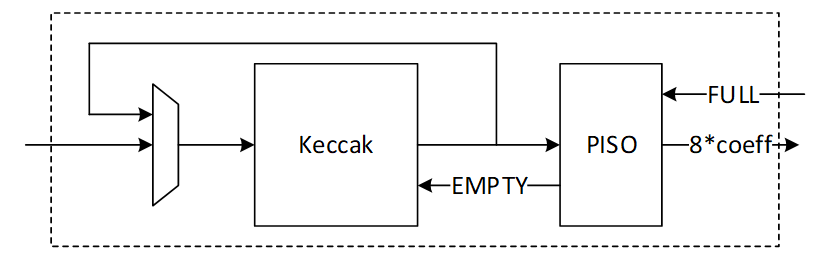
SampleInBall architecture
SampleInBall is a procedure that uses the SHAKE256 of a seed ρ to produce a random element of Bτ. The procedure uses the Fisher-Yates shuffle method. The signs of the nonzero entries of c are determined by the first 8 bytes of H(ρ), and the following bytes of H(ρ) are used to determine the locations of those nonzero entries.
We propose an architecture to remove the cost of memory access from Keccak to SampleInBall, and from SampleInBall to NTT. This requires a specific pattern of coefficients for NTT that prevents excessive buffering or interference between them. It also lowers the rejection rate and speeds up SampleInBall while maintaining small and efficient architecture.
High-level architecture is illustrated as follows:
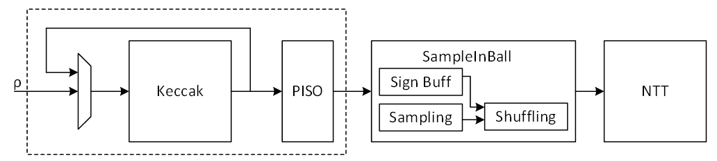
Keccak interface to SampleInBall
Keccak is used in SHAKE-256 configuration for SampleInBall operation. Hence, it will take the input seed with 256-bit and generates 1088-bit output after each round.
The first τ bits (τ = 60 in the case of ML-DSA-87) in the first 8 bytes of this random stream are interpreted as τ random sign bits si ∈ {0, 1}, i = 0, . . . , τ − 1. The remaining 64 − τ bits are discarded.
The remaining random bits are used for sampling. Since each 8-bit is used for one sample, the first round of Keccak output provides (1088-64)/8=128 samples. The number of valid samples needed is 60. Because this is a sampling operation that is non-deterministic, if more samples are required, Keccak will run again and produce 1088/8=136 additional samples. Hence, there are two paths for Keccak input. While the input seed can be set by controller for each new polynomial c, the loop path is used to rerun Keccak for completing the previous polynomial.
SampleInBall cannot take all samples parallelly since it makes hardware architecture too costly and complex. Therefore, we propose a parallel-input serial-output (PISO) unit in between to store the Keccak output and feed SampleInBall unit sequentially.
SampleInBall
This unit takes data from the output of SHAKE-256 stored in a PISO buffer. The required cycles for this unit are variable due to the non-deterministic pattern of sampling. But this operation can only be finished with 60 valid samples.
In our optimized architecture, this unit works in parallel with the Keccak core. Therefore, the latency for Keccak sampling (for the second round and next) is absorbed within the latency for a concurrently running SampleInBall core.
The NTT unit needs to take four coefficients per cycle. This implies that the output contains four samples per each address as follows:
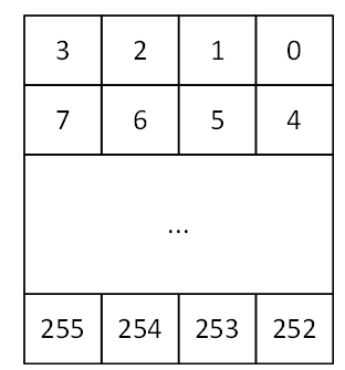
SampleInBall algorithm is as follows:
1) Initialize c = c0 c1 . . . c255 = 0 0 . . . 0
2) for i := 256 − τ to 255
3)     j ← {0, 1, . . . , i}
4)     s ← {0, 1}
5)     ci := cj
6)     cj := (−1)s
7) return c
SampleInBall includes three main operations:
- Check the validity of input samples respect to parameter i (line 3 of algorithm)
- Store the sign s (line 4 of algorithm)
- Shuffle the stored polynomial c respect to parameter i, j, and s (line 5 and 6 of algorithm)
To recall, for ML-DSA-87 with τ = 60, 60 valid samples are required.
Validity check on the input sample depends on the iteration number i while a sample greater than i will be rejected. Hence, the probability of failure for each round would be:
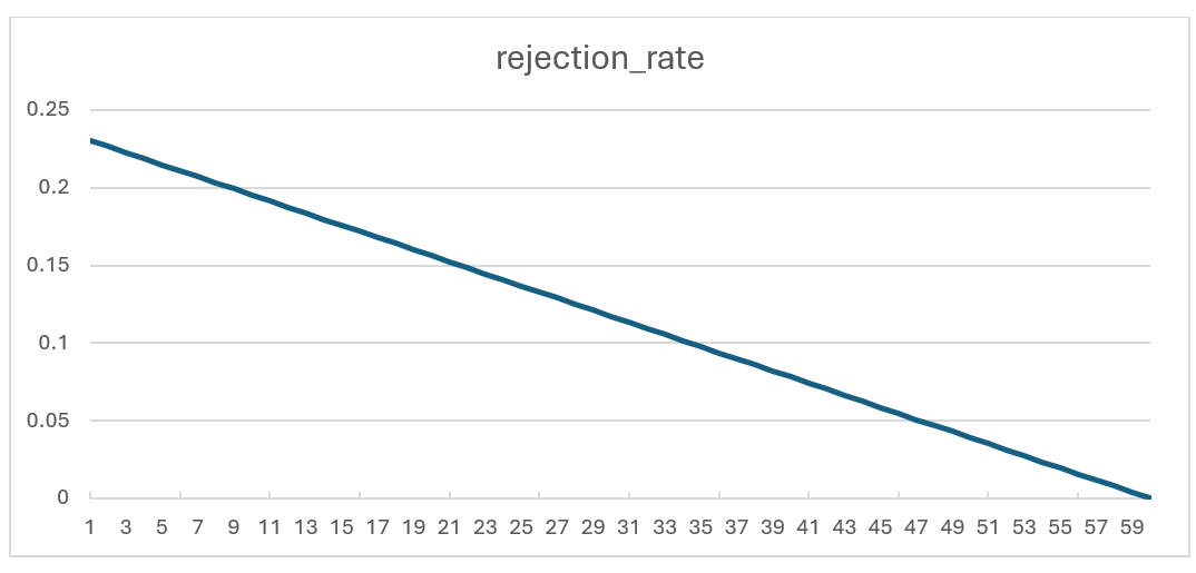
Rejection rate for each round of SampleInBall operation
To reduce the failure probability and avoid any wait cycle in polynomial multiplication, 4 samples are fed into SampleInBall while only 1 of them will be passed to shuffling unit. This decision reduces the probability of failure to:
\(probability of having 4 rejected inputs=(rejection rate)^4\)
In the worst case scenario (the first iteration with i=196), the failure probability is:
\((0.23046)^4=0.00282\)
The unused coefficients will be processed in the next cycle when i increments. The architecture is as follows:
Sampling phase of SampleInBall architecture
The first 2 cycles is used to store the sign bits into the sign buffer. After that, each 32 bits of input will be divided into 4 samples. Each sample is compared to i and the first valid sample is passed into the shuffling step.
Controller uses a counter to manage i value. The counter starts at 196 (for ML-DSA-87) and goes up after a valid coefficient is found.
When a valid coefficient is found, valid flag will be set and the chosen sample (known by j), i, and s will be transferred to shuffling unit. Then, the counter is incremented, and the remaining samples will be compared to the new i value.
The architecture of shuffling unit is as follows:
Shuffling phase of SampleInBall architecture
A polynomial c is stored in a memory that has four coefficients for each address. This pattern is needed for NTT operation that works on the output of SampleInBall. The memory has two ports that can read or write data.
Each input sample needs two cycles. In the first cycle, the memory reads the two addresses that have i and j, and in the second cycle, the memory saves the new coefficients.
The read data from address j will be updated with 1 or q-1 based on the s value, while the original value of j is transferred to address i using a multiplexer and demultiplexer.
When i and j have the same address, both ports try to write to the same location in the second cycle. To avoid this, the red path is used to turn off port a for address j. But then, j will be changed in the same buffer that has i (port b) and will be saved into memory.
Decompose Architecture
Decompose unit is used in signing operation of Dilithium. It decomposes r into (r1,r0) such that r ≡ r1(2γ2)+r0 mod q. The output of decompose has two parts. While r0 will be stored into memory, r1 will be encoded and then be stored into Keccak SIPO input buffer to run SHAKE256.
There are k polynomials (k=8 for ML-DSA-87) that needs to be decomposed as follows:
\[ w= \begin{bmatrix} w_0 \ \vdots \ w_{k-1} \end{bmatrix} \]
Due to our memory configuration that stores 4 coefficients per address, we need 4 parallel cores for decompose and encode units to match the throughout between these modules.
Decompose algorithm plays a crucial role by breaking down the coefficients of a polynomial into smaller parts. Decompose calculates high and low bits r1 and r0 such that:
\[ r = r_1 · 2 γ_2 + r_0 {mod} q \]
where:
\[ -γ2 < r0 \leq γ2 \]
except for the border case when r - r0=q – 1. In the border case, the high bits r1 are made zero, and the low bits r0 are reduced by one.
Definition:
- mod α: If α is a positive integer and m ∈ Z or m ∈ Zα, then m mod α denotes the unique element m ′∈ Z in the range 0 ≤ m ′ < α such that m and m ′ are congruent modulo α.
- mod± α: If α is a positive integer and m ∈ Z or m ∈ Zα, then m mod± α denotes the unique element m ′∈ Z in the range −α/2 < m ′ ≤ α/2 such that m and m ′ are congruent modulo α.
High-level architecture is illustrated as follows:
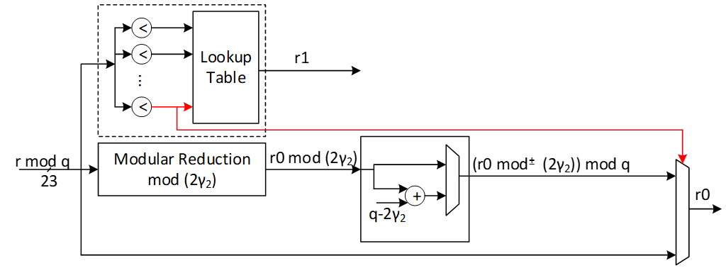
The modular reduction architecture is as follows:
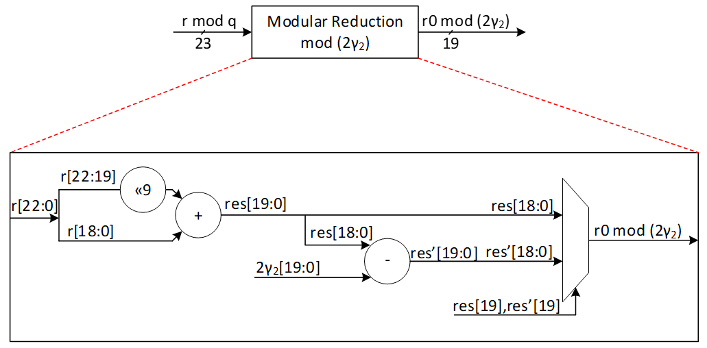
| r0 mod 22 down limit | r0 mod 22 Up limit | r0 |
|---|---|---|
| 0 | γ2 | r0 mod 2 γ2 |
| γ2+1 | 2γ2-1 | (r0 mod 2 γ2) + (q-2 γ2) |
Our suggested design calculates two shares of r0 and r1 at the same time. We use a lookup table with 16 parallel comparisons to find the value of r1 from r based on the following graph:
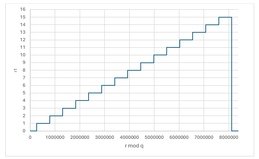
r1 value based on the given r
| r down limit | r Up limit | r1 |
|---|---|---|
| 0 | γ2 | 0 |
| γ2+1 | 3γ2 | 1 |
| 3γ2+1 | 5γ2 | 2 |
| 5γ2+1 | 7γ2 | 3 |
| 7γ2+1 | 9γ2 | 4 |
| 9γ2+1 | 11γ2 | 5 |
| 11γ2+1 | 13γ2 | 6 |
| 13γ2+1 | 15γ2 | 7 |
| 15γ2+1 | 17γ2 | 8 |
| 17γ2+1 | 19γ2 | 9 |
| 19γ2+1 | 21γ2 | 10 |
| 21γ2+1 | 23γ2 | 11 |
| 23γ2+1 | 25γ2 | 12 |
| 25γ2+1 | 27γ2 | 13 |
| 27γ2+1 | 29γ2 | 14 |
| 29γ2+1 | 31γ2 | 15 |
| 31γ2+1 | q-1 | 0 |
To compute r0 mod± 2γ2, at the same time with r1 computation, a modular reduction operation will be applied to the input value r with respect to 2γ2 to compute r0 mod 2γ2. The result can be mapped into mod± 2γ2 range by subtracting 2γ2 when the result is greater than γ2. However, at the end all shares should be modulus q. For that, instead of subtracting 2γ2, we perform an addition with q-2γ2 to the results.
The expected r0 for different values of r is illustrated as follows:
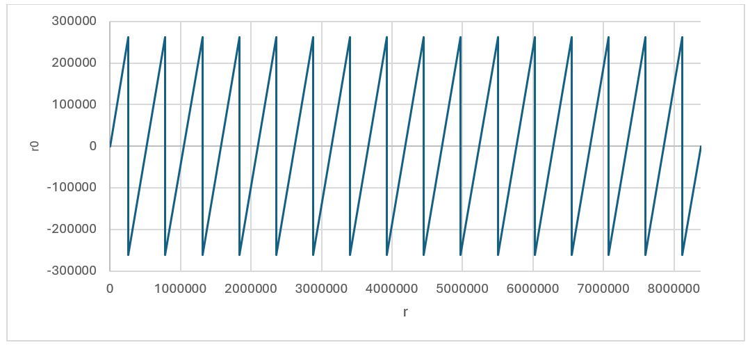
r0 value based on the given r (without considering boarder case)
Using this technique, we could achieve r0 and r1 for all cases expect the border case where r - r0=q – 1. This case can be detected inside r1 decompose architecture shown by red. In this case, the lookup table sets the value of 0 for r1, while r1 will be set as follows:
r0=r0-1=r-q+1-1=r-q≡r mod q
r0 value based on the given r considering boarder case
Performance of Decompose
There are k polynomials with 256 coefficients for each that need to be fed into decompose unit in pipeline method. After having 1088-bit input into SIPO, Keccak will be enabled parallel with decompose and encode units. However, the last round of Keccak will be performed after processing all coefficients. Each round of Keccak takes 12 cycles which allows processing of 48 coefficients. Since the output length of each encode unit is 4 bits, Keccak works faster than decompose/encode units and SIPO will not have overflow issue.
For a complete decompose/encode/hash operation for Dilithium ML-DSA-87 with 8 polynomials, 8*256/4 + 12 = 524 cycles are required using pipelined architecture.
MakeHint Architecture
The basic approach of the MakeHint(z, r) function involves decomposing both r and r+z into two parts: (r1, r0) for r and (rz1, rz0) for r+z. It then proceeds to evaluate whether r1 and rz1 are identical. In the event that r1 does not match rz1, it indicates that a hint is necessary to proceed. This process is essential for determining when additional information is required to resolve discrepancies between the compared segments.
However, decompose function is expensive on hardware to be implemented. Furthermore, performing a sequential decompose function using a shared hardware resource requires more latency.
The process of implementing the decompose function is notably resource-intensive and can incur significant costs when executed on hardware. Additionally, the sequential execution of this function, particularly when it relies on a common hardware resource, tends to introduce increased latency. This is due to the fact that shared resources often necessitate additional time to manage concurrent operations, which can result in delays and reduced efficiency.
The following architecture shows Dilithium algorithm to compute h=MakeHint(−ct0, w − cs2 + ct0). There are several decompose operations embedded into HighBits, LowBits, and MakeHint functions, shown by red.
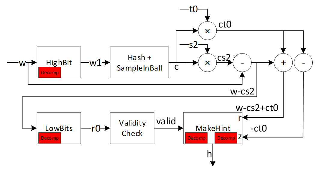
As an alternative and more efficient way, we can use a method to realize where hint needs to be generated as follows:
To compute h=MakeHint(−ct0, w − cs2 + ct0), first note is that instead of computing (r1, r0) = Decomposeq (w−cs2, α) and checking whether ‖r0‖<2 - β and r1 = w1, it is equivalent to just check that ‖w0-cs2‖<2-β, where w0 is the low part of w. If this check passes, w0 − cs2 is the low part of w − cs2. Next, recall that by the definition of the MakeHint function, a coefficient of a polynomial in h as computed is non-zero precisely if the high parts of the corresponding coefficients of w − cs2 and w − cs2 + ct0 differ. Now, we have already computed the full decomposition w = αw1 + w0 of w, and we know that αw1 + (w0 −cs2) is the correct decomposition of w−cs2. But then, αw1 + (w0 −cs2 +ct0) is the correct decomposition of w − cs2 + ct0 (i.e. the high part is w1) if and only if each coefficient of w0 − cs2 + ct0 lies in the interval (−γ2, γ2], or, when some coefficient is −γ2 and the corresponding coefficient of w1 is zero. The last condition is due to the border case in the Decompose function. On the other hand, if these conditions are not true, then the high parts must differ, and it then follows that for computing the hint vector h it suffices to just check these conditions on the coefficients of w0 − cs2 + ct0. This algorithm is shown as follows:
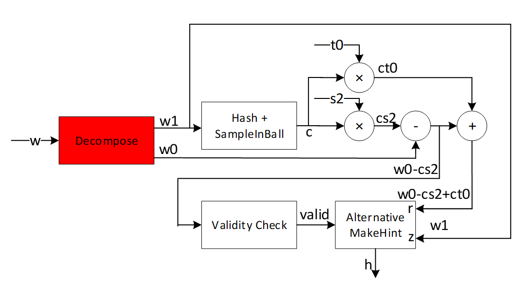
The alternative algorithm reduces the decompose cost by modifying the MakeHint to enhance the efficiency of the architecture. We propose efficient architecture for performing the alternative MakeHint operation on hardware platform and accelerate this operation using a pipeline architecture.
High-level architecture is illustrated as follows:
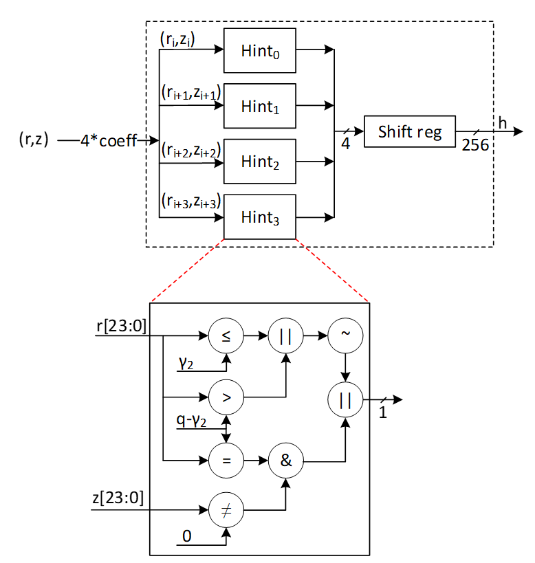
Hint Sum and Hint BitPack
In Dilithium signing algorithm, the output of Makehint (hint output) is further processed to generate the encoded ‘h’ component of the signature. Additionally, one of the validity checks in signing algorithm uses hint sum to determine validity of the generated signature. These post-processing steps can be embedded into the Makehint architecture to avoid latency overhead while maintaining low complexity. The following figure shows the embedded logic into Makehint to generate the required outputs.
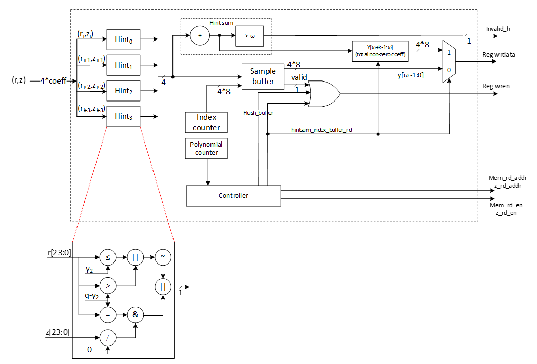
Hint Sum:
In the pipelined architecture, as 4 hints are generated every cycle, they are accumulated every cycle for all 8 polynomials.
{if hintsum> ω invalid_h=1 else invalid_h=0
Hint BitPack:
The output of hint bitpack is a byte string ‘y’ of which [ω-1:0] bytes are the indices at which the generated hint is non-zero. [ω+k-1 : ω] bytes are the total number of indices per polynomial at which the hint is non-zero. If the number of non-zero hints is < ω, the rest of the entries of y are filled with 0s. If the number of non-zero hints is > ω, Makehint flow continues for the remaining coefficients and the ‘y’ array is overwritten with the subsequent values. In this case, the ‘h’ component is invalid and the signature is discarded.
The following table shows an example of construction of y array per polynomial based on generated hints.
| Polynomial | Hint[3:0] | Index[3:0][7:0] | y[ω-1:0] |
|---|---|---|---|
| 0 | 1-1-0-0 | 3-2-1-0 | 3-2 |
| 0 | 0-1-0-1 | 7-6-5-4 | 6-4-3-2 |
| 0 | 0-0-1-0 | 11-10-9-8 | 9-6-4-3-2 |
| … | … | … | …-9-6-4-3-2 |
| 1 | 1-1-1-0 | 3-2-1-0 | 3-2-1-…-9-6-4-3-2 |
| 1 | 0-1-1-0 | 7-6-5-4 | 6-5-3-2-1-…-9-6-4-3-2 |
| … | … | … | …-6-5-3-2-1-…-9-6-4-3-2 |
| 2 | 0-0-0-0 | 3-2-1-0 | …-6-5-3-2-1-…-9-6-4-3-2 |
| 2 | 0-0-0-1 | 7-6-5-4 | 4-…-6-5-3-2-1-…-9-6-4-3-2 |
| 2 | 1-1-0-0 | 11-10-9-8 | 11-10-4-…-6-5-3-2-1-…-9-6-4-3-2 |
| … | … | … | … |
To optimize area, 1 dword of ‘y’ buffer is written directly to the register API. The buffer generates a valid signal after accumulating 1 dword worth of data which can be used as a write enable for the register API. To protect the signature from intermittent firmware reads, the signature register is lockable. The lock is asserted during signing flow and is only unlocked after the entire flow has been completed.
At the end of all polynomials, the hintsum is written to the register API to construct the y[ω+k-1:ω] locations of the byte string.
It is possible that during the last cycle of the last polynomial, the index buffer contains < 1 dword of index values to be written to the reg API. To accommodate this scenario, the controller flushes out the buffer at the end of the last polynomial and writes the remaining data to the register API.
W1Encode Architecture
The signer’s commitment is shown by w, while this value needs to be decomposed into two shares to provide the required hint as a part of signature. The output of decompose is shown by (w1, w0) which presents the higher and lower parts of the given input. While w0 can be stored into the memory, the value of w1 is required to compute commitment hash using SHAKE256 operation. The following equation shows this operation:
c=H(μ||w1Encodew1)
Where is a 512-bit value computed based on the message and || means the concatenation between these two parts.
In ML-DSA-87 algorithm, there are 8 polynomials for w shown by w0 to w7. Furthermore, higher parts of each coefficient of these polynomials, shown by w1, is a value in [0:15] range that can be presented by 4 bits. Based on this, the total input size for performing SHAKE256 is:
inputsize=512size of μ+8poly number*256coeff per poly*4higher bit per coeff=8,704 bits
Since SHAKE256 takes only 1088 bits per each round, we have to feed these values sequentially. However, due to the prefix value of , and also the SHAKE256 input size does not divide evenly by each polynomial w1 size (which is 256*4=1024 bits), the pattern of feeding decompose results into hashing buffer is challenging.
There are k polynomials (k=8 for ML-DSA-87) that needs to be decomposed as follows:
\[ w= \begin{bmatrix} w_0 \ \vdots \ w_{k-1} \end{bmatrix} \]
Due to our memory configuration that stores 4 coefficients per address, we need 4 parallel cores for decompose and encode units to match the throughout between these modules.
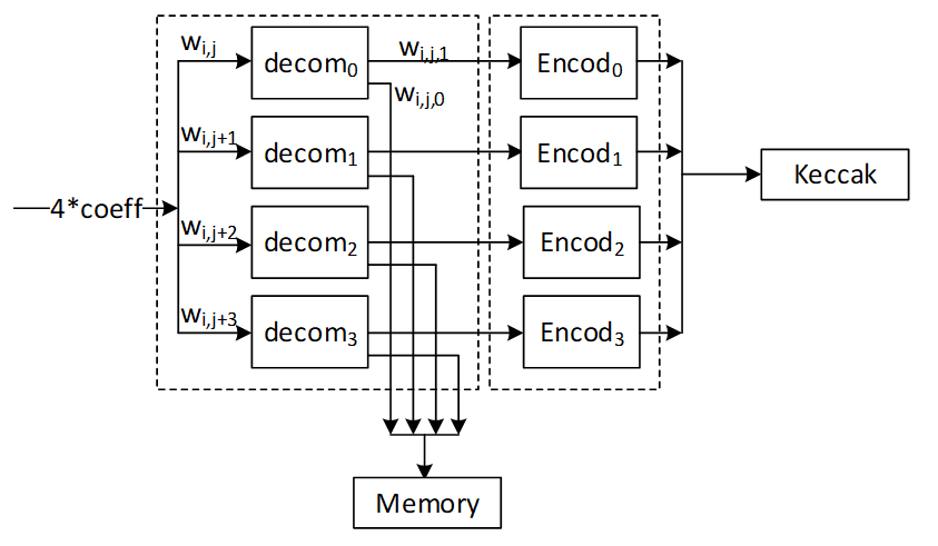
To optimize the performance and remove the cost of memory, we use a pipeline architecture for encode that processes the input values and feed them into Keccak buffer. The following figure shows the optimized architecture for W1Encoder.
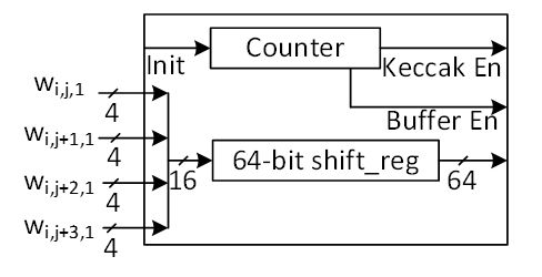
In the suggested design, every cycle, 4 coefficients for w1 are calculated from the decompose unit and then sent to the encode unit. Each coefficient is represented by 4 bits, making a total of 16 bits. However, the Keccak buffer only accepts input in 64-bit chunks. Therefore, a shift register is used to store the coefficients and pass a 64-bit chunk every 4 cycles to the Keccak SIPO buffer. An internal counter is used to control when the Keccak SIPO buffer takes this 64-bit chunk every 4 cycles.
Meanwhile, Keccak SIPO buffer can store 1088 bits of data and then activate Keccak to process it. The internal counter counts the number of writes on Keccak SIPO, and when it reaches 17 (17*64 = 1088 bits), Keccak enable is triggered. Because of Keccak architecture, SIPO can keep buffering a new input while Keccak works on the previous stored data.
The very first iteration of Keccak contains a 512-bit value shown by , which the high-level controller puts in Keccak SIPO buffer before decompose/encode process. So, only 576 bits of SIPO are left for encoding output. We suggest starting with a counter value of 8 to deal with this edge case in the first Keccak round. The other rounds have 17 SIPO write enable.
The following figure shows the counter architecture. The first two bits is used to enable SIPO buffer, while the remaining bits of [6:2] is used to enable Keccak process.
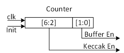
The following table reports the SIPO input for different Keccak rounds.
| Keccak SHAKE256 Round | Buffer input | Bits |
|---|---|---|
| 1 | μ | 512 |
| w0[143:0] | 576 | |
| 2 | w0[255:144] | 448 |
| w1[159:0] | 640 | |
| 3 | w1[255:160] | 384 |
| w2[175:0] | 704 | |
| 4 | w2[255:176] | 320 |
| w3[191:0] | 768 | |
| 5 | w3[255:192] | 256 |
| w4[207:0] | 832 | |
| 6 | w4[255:208] | 192 |
| w5[223:0] | 896 | |
| 7 | w5[255:224] | 128 |
| w6[239:0] | 960 | |
| 8 | w6[255:240] | 64 |
| w7[255:0] | 1024 | |
| 9 | padding | 1088 |
When the whole polynomials are done in the first 8 rounds of Keccak and Keccak done signal is asserted, the encode done signal is asserted and the high-level controller resumes control and adds the necessary padding to SIPO to finish the SHAKE256 process.
Norm Check Architecture
The figure provided illustrates the finite field range for polynomial coefficients. It indicates that each coefficient is an integer ranging from 0 to q-1:

The infinity norm is defined as follows:
For an element w ∈ Z , \(∥w∥∞ = |w|\), the absolute value of w. For an element \(w ∈ Z_q\),\(∥w∥∞ = w mod^ ± q\) . For an element w of R or Rq, \(∥w∥∞ = max0≤i<256 ∥wi∥∞\) . For a length-m vector w with entries from R or Rq, \(∥w∥∞ = max0≤i<m ∥w[i]∥∞\) .
In the context of norm definition within a finite field, when a value for the bound is provided, the norm check determines whether the coefficient falls below the bound or exceeds the q-bound, which is highlighted in red in the following figure.

There are three different validity checks with different bounds during signing operations as follows:
- \[ |(|z|)|_∞ ≥ γ1 -β \]
- \[ |(|r0|)|_∞ ≥ γ2 -β \]
- \[ |⟨⟨ct0⟩⟩|_∞ ≥ γ2 \]
Vector z contains l polynomials (l=7 for ML-DSA-87) and r0 and ct0 contains k polynomials (k=8 for ML-DSA-87) that needs to be evaluated by norm check operation.
Due to our memory configuration that stores 4 coefficients per address, we need 4 parallel cores for norm check unit to match the throughput between these modules. To optimize the performance and remove the cost of memory, we use a pipeline architecture for norm check that processes the input values.
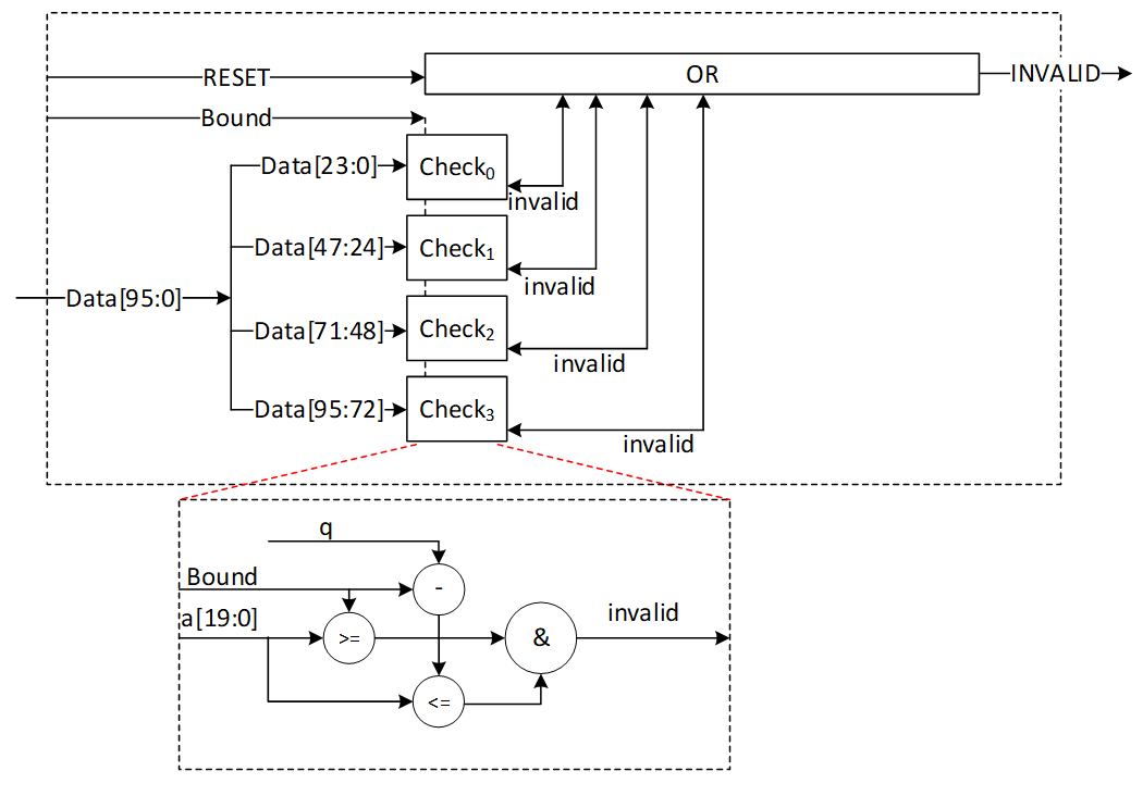
In the proposed design, during each cycle, 4 norm check coefficients are computed from stored data. This provides a performance improvement since this block only needs to read from memory and does not perform any writes to memory. Every coefficient is expressed using 24 bits, culminating in a combined total of 96 bits. A norm check is executed on each of these coefficients to produce a invalid output. The invalid outputs for all coefficients across all polynomials must be collectively ORed to yield the ultimate INVALID signal. This INVALID signal is asserted when any coefficient fails to meet the predetermined norm check criteria within the specified bound.
The proposed design is configurable and accepts different bounds to reduce the required hardware resources. The following table shows the latency requirements for these three norm checks.
| Input polynomials | Number of polynomials | Total coefficients | Latency for ML-DSA-87 |
|---|---|---|---|
| z | L | L*256 | 448 (for 4) |
| r0 | K | K*256 | 512 (for 4) |
| ct0 | k | K*256 | 512 (for 4) |
skDecode Architecture
The given sk to the core for performing a signing operation has been encoded, and skDecode is responsible to reverse the encoding procedure to divide sk to the appropriate portions. The initial segments within sk should be allocated to variables p, K, and tr, corresponding to sizes of 256 bits, 256 bits, and 512 bits, respectively, without necessitating any modifications.
The remaining part of sk stores the packed form of s1, s2, and t0, respectively. For s1 and s2, each coefficient is represented by η bits and needs to be unpacked as follows:
coefficient = η – data[η_size-1:0]
where η_size = bitlen(2*η).
For t0, each coefficient is represented by d bits and needs to be unpacked as follows:
coefficient = 2d-1 – data[d-1:0]
| sk part | poly size | coeff size | Total size | Latency for ML-DSA-87 |
|---|---|---|---|---|
| s1 | l=7 | η_size=3 | l*256*η_size=7*256*3= 5376 | 224 cycles |
| s2 | k=8 | η_size=3 | k*256*η_size =8*256*3= 6144 | 256 cycles |
| t0 | K=8 | d=13 | k*256*d=8*256*13= 26624 | 256 cycles (using 8 parallel cores) 512 cycles (using 4 parallel cores) |
The skDecode architecture reads 8 values from the register API, based on the memory pattern that has 4 coefficients for each address. It then maps them to modulo q value using the given equation. Then it stores the mapped value in the memory with two parallel write operations.
The high-level architecture for skDecode is as follows:
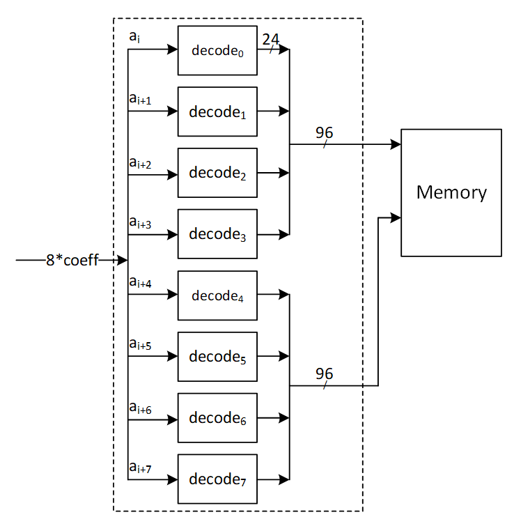
For s1 and s2 unpacking, the decode architecture is as follows:
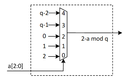
In case a[2:0] is greater than ‘h4, the sk is considered out of range. skDecode block triggers an error interrupt to the RV core and the algorithm is aborted.
For t0 unpacking, the decode architecture is shown below:
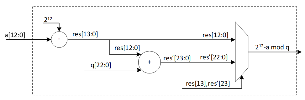
Since key sizes are large, a key memory is used to interface with FW and skDecode module to avoid routing and timing issues. Assuming a memory interface of two 32-bit RW ports, s1s2 unpacking can be done with 8 parallel cores. This requires 24-bits per cycle to be processed which can be accommodated with a single key memory read per cycle (32-bits) and accumulating remaining bits in a sample buffer. Once next read occurs, bits are appended to the previous ones and the values are fed from buffer to the unpack module.
In case of t0 unpacking, since 13-bits are required per core, 4 parallel cores can be used instead of 8 to support the 32-bit memory interface. Two memory reads are done per cycle (64-bits) and 52 bits are processed per cycle (13*4). Remaining bits are accumulated in the sample buffer and read out.
The s1/s2 buffer can hold up to 32+24 bits of data. To avoid data conflict within s1/s2 buffer, the following memory access pattern is used:
S1, s2 unpack:
Cycle 0 🡪 read 1 addr (buffer = 32 bits)
Cycle 1 🡪 read 1 addr (buffer = 32 + 8 bits)
Cycle 2 🡪 read 1 addr (buffer = 32 + 16 bits)
Cycle 3 🡪 stall and read buffer contents (24 bits)
T0 unpack:
In case of t0 unpack, the t0 sample buffer can hold up to 64+52 = 116 bits of data. The buffer generates a full signal that is used to stall key memory reads for a cycle before continuing to write to the buffer.
sigEncode_z Architecture
The sigEncode_z operation converts a signature into a sequence of bytes. This operation has three distinct parts, namely c, z, and h. The first part simply writes the c into the register API as it is. The last part also uses the MakeHint structure to combine the MakeHint outputs into register API. However, the middle part, that is z, requires encoding.
Every coefficient of z is between [-γ1+1, γ1], but its value mod q is kept in memory. To encode it, this equation is needed on the non-modular value:
Encoded z = γ1 – z
The high-level architecture processes each coefficient of z in this way:
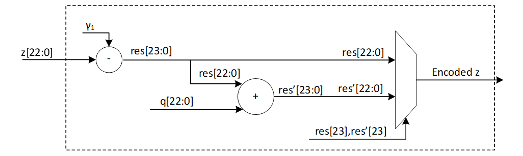
The modular and non-modular value are equal when the z is in the interval [0, γ1]. The first branch in this architecture shows this. But for the negative range, we need to remove q from the difference results. In this case, we get γ1 – (z mod q) = γ1 – (q + z) = γ1 – z – q. So, the second branch adds q to the result to finish the encoding.
Using two parallel read ports, 8 encoding units read 8 coefficients from the memory and write the encoded values to the register API as follows:
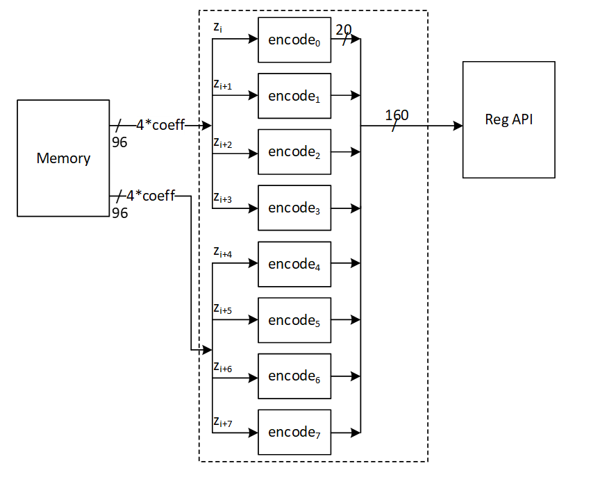
Power2Round Architecture
Power2Round function is used to split each coefficient of vector t to two parts (similar to decompose unit). Power2Round calculates high and low bits r1 and r0 such that:
r = r1 · 2d +r0 mod q
where:
\(-2^(d-1)<r_0≤2^(d-1)\)
Definition:
- mod α: If α is a positive integer and m ∈ Z or m ∈ Zα, then m mod α denotes the unique element m ′∈ Z in the range 0 ≤ m ′ < α such that m and m ′ are congruent modulo α.
- mod± α: If α is a positive integer and m ∈ Z or m ∈ Zα, then m mod± α denotes the unique element m ′∈ Z in the range −α/2 < m ′ ≤ α/2 such that m and m ′ are congruent modulo α.
The power2round process yields two outputs, t0 and t1. The value of t0 must be processed using skEncode and then placed in the API register. Meanwhile, t1 is to be processed with pkEncode and then fed into the register API. This is depicted in the high-level architecture diagram.
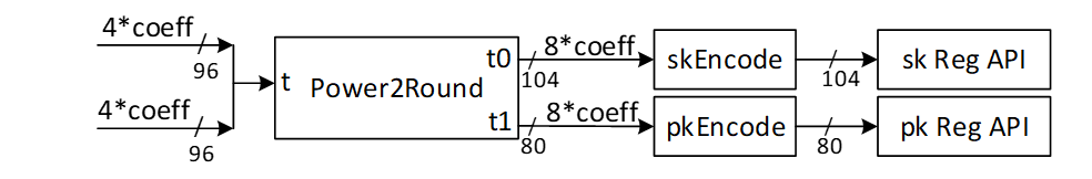
The goal is to create a pipeline architecture for skEncode and pkEncode that minimizes memory overhead costs. Therefore, these operations will be executed simultaneously with power2round, and the outcomes will be directly stored into the API.
Power2Round reads 2 addresses of memory containing 8 coefficients.
The expected r1 and r0 for different values of given r is illustrated as follows:

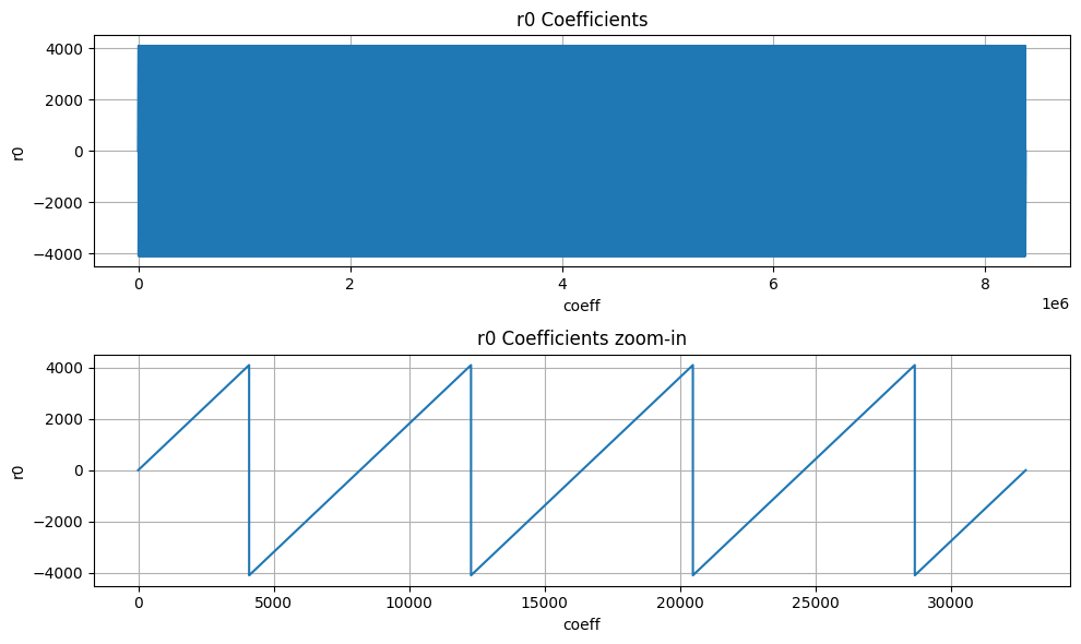
The diagram illustrates the structure of the power2round mechanism integrated with the skEncode arrangement. However, pkEncode is the process of saving the t1 values into the register API.
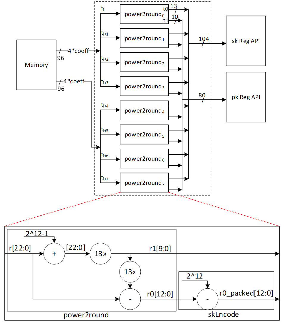
skEncode Architecture
The SkEncode operation requires multiple inputs (skEncode(ρ, K, tr, s1, s2, t0)). But ρ, K, tr, and t0 have been preloaded into the API through different operations. In terms of s1 and s2, SkEncode serves as a conversion tool that maps the values of these coefficients using the following equation:
data[η_size-1:0] = η – coefficient
For ML-DSA-87 with η=2, there are only 5 possible values for the s1 and s2 coefficients, and the following architecture converts their modular presentation into the packed format:
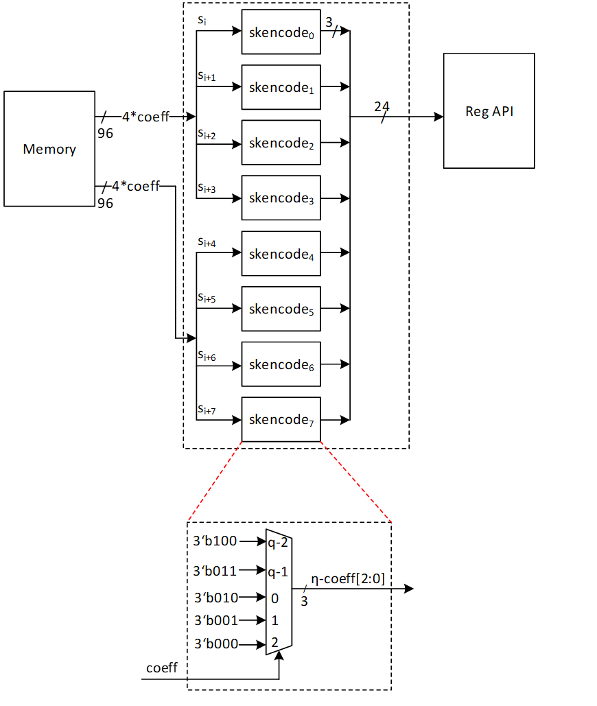
pkDecode Architecture
During the verification process, the provided pk must be decoded. The initial 256 bits of pk include ρ exactly as it is. The bits that follow consist of t1 polynomials. According to ML-DSA-87 protocol, each set of 10 bits represents a single coefficient. Therefore, these 10 bits need to be read, shifted left by 13 bits, and the outcome should be saved into memory.
The architecture is as follows:
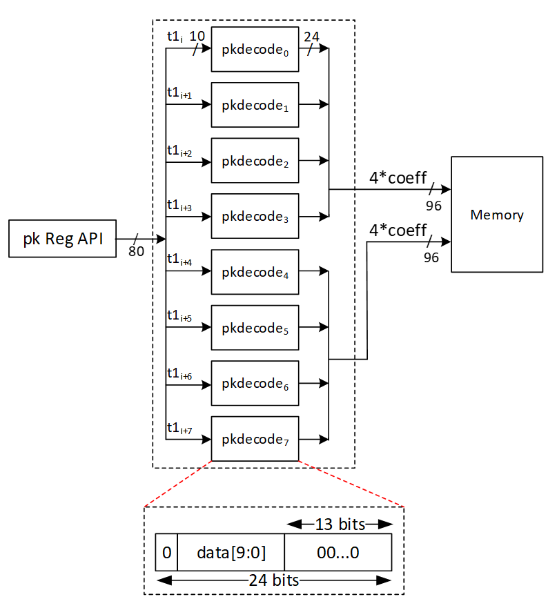
sigDecode_z Architecture
The sigDecode operation reverses the sigEncode. This operation has three distinct parts, namely c, z, and h. The first part simply writes the c from the register API as it is. The last part also uses the HintBitUnpack structure to combine the MakeHint outputs into register API. However, the middle part, that is z, requires decoding.
Every coefficient of z is presented by 20 bits, but its value mod q is required to be stored into memory. To decode it, this equation is needed:
Decoded z = γ1 – z
However, because the decoded value falls within [-γ1+1, γ1], we must convert it to its equivalent modular q value.
The high-level architecture is as follows:
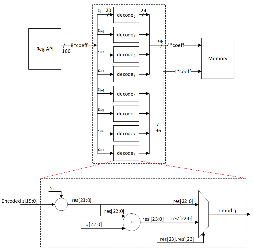
sigDecode_h Architecture
The sigDecode function reverses sigEncode and is composed of three separate segments: c, z, and h. The h part uses the HintBitUnpack structure to decode given Hint and store it into memory.
We must reconstruct k polynomials (with k being 8 in the case of ML-DSA-87) using the decoding process provided. The total number of non-zero indices of each polynomial can be found in the range of bytes [ω: ω+k-1] (where ω is set to 75 for ML-DAS-87). Therefore, the initial step to reconstruct each hi involves reading the byte at position ω+i for each polynomial (where 0≤i<k), shown by HINTSUM_i.
HINTSUM_i indicates how many bytes to read from [ω-1:0] byte range for the current polynomial from the register API. To keep the API constant and avoid any complexity in storing hints for the next polynomial, the decode module always reads 4 bytes from the register API and an internal vector, current polynomial map (curr_poly_map), is used to indicate which of the 4 bytes belongs to the current polynomial. For example, if the HINTSUM is 3, the curr_poly_map is updated to 0-1-1-1 to indicate that bytes [2:0] are valid. Byte[3] is processed as part of the next polynomial. Once the required bytes are identified, a 256-bit vector is updated with 1s in the positions indicated by these input bytes. After the first cycle, the first 4 bits of the bitmap are ready to be written to the memory.
To keep the throughput as storing 4 coefficients per cycle into internal memory, hints are processed every cycle and the bitmap is updated every cycle. To store data into memory, each coefficient, which might either be a 0 or a 1, is represented using 24 bits.
Since a non-zero hint can occur in any position of the 256-bit vector, it takes 64 cycles (4 coeffs/cycle) to write all 256 coefficients to memory irrespective of the value of the coefficient. For example, if the last 1 recorded is in index 35, the decode module continues to write the rest of the coefficients (36, 37, etc) to memory.
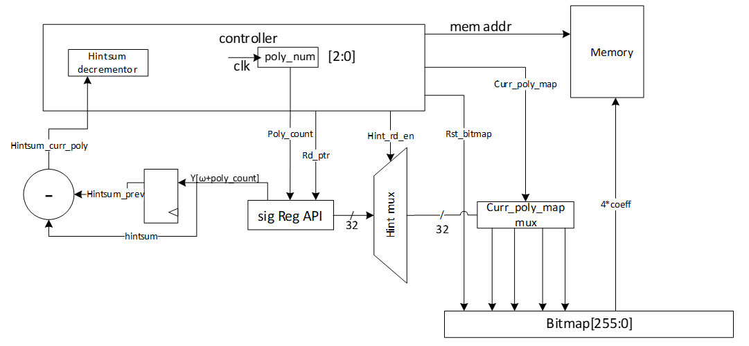
Example hint processing:
| Cycle | Polynomial | Hintsum | Hintsum_curr | Remaining hintsum | Byte select of reg API | Curr_poly_map |
|---|---|---|---|---|---|---|
| 0 | 0 | 5 | 5 | 5 | 3-2-1-0 | 1-1-1-1 |
| 1 | 0 | 5 | 5 | 5-4 = 1 | 7-6-5-4 | 0-0-0-1 |
| 2-63 | 0 | 5 | 5 | 0 | - | 0-0-0-0 |
| 64 | 1 | 11 | 11-5 = 6 | 6 | 8-7-6-5 | 1-1-1-1 |
| 65 | 1 | 11 | 6 | 6-4 = 2 | 12-11-10-9 | 0-0-1-1 |
| 66-127 | 1 | 11 | 6 | 0 | - | 0-0-0-0 |
| 128 | 2 | 25 | 25-11 = 14 | 14 | 14-13-12-11 | 1-1-1-1 |
| 129 | 2 | 25 | 14 | 14-4 = 10 | 18-17-16-15 | 1-1-1-1 |
| 130 | 2 | 25 | 14 | 10-4 = 6 | 22-21-20-19 | 1-1-1-1 |
| 131 | 2 | 25 | 14 | 6-4 = 2 | 26-25-24-23 | 0-0-1-1 |
In each cycle, the positions indicated by y[rd_ptr] are flipped to 1 in the bitmap. Once a polynomial is finished, the bitmap, read pointer, current polynomial map, etc are all reset to prepare for the next polynomial. In this way, sigdecode_h takes (64*8 = 512) cycles to finish writing all coefficients to the internal memory (a few additional cycles are required for control state transitions).
Hint rules
The hint (h segment of the signature) must follow a specific pattern. Any violation of these rules renders the hint (and signature) invalid. In such cases, the sigDecode_h architecture raises an error, causing the verification process to fail. The structure of h is as follows:
| Byte 0 | Byte 1 | Byte 2 | ... | Byte ω-1 | Byte ω | Byte ω+1 | ... | Byte ω+k-1 |
|---|---|---|---|---|---|---|---|---|
| Hint_0 | Hint_1 | Hint_2 | ... | Hint_ω-1 | HINTSUM_0 | HINTSUM_1 | ... | HINTSUM_k-1 |
-
HINTSUM_0 represents the number of non-zero coefficients in poly_0.
-
For subsequent polynomials (poly_i, where i > 0), the number of non-zero coefficients is determined by HINTSUM_i - HINTSUM_(i-1).
The rules for a valid hint are as follows:
- The HINTSUM_i values must be in ascending order. Repeated values are allowed, meaning a polynomial may have no non-zero coefficients.
- The maximum allowable value for HINTSUM_i is ω. Since the values must be in ascending order, if HINTSUM_i = ω for any i < k-1, then all subsequent HINTSUM values must also be ω.
- Within each polynomial, non-zero coefficient indices must be unique and arranged in ascending order.
- If HINTSUM_(k-1) is less than ω, all hint values from Hint_(HINTSUM_(k-1)) to Hint_(ω-1) must be zero.
UseHint Architecture
To reconstruct the signer's commitment, it is necessary to update the approximate computed value labeled as w' by utilizing the provided hint. Hence, the value of w’ should be decomposed, and its higher part should be altered if the related hint equals 1 for that coefficient. Subsequently, the higher part requires encoding through the W1Encode operation and must be stored into the Keccak SIPO.
The procedure is similar to the Decompose and W1Encode steps in the signing process, but it differs since there's no need to store the lower segment in memory. Moreover, the UseHint operation occurs between Decompose and W1Encode, adjusting the upper portion of the Decompose output utilizing h.
The Decompose and W1Encode stages of the signing procedure are depicted below (with the gray components being inactive):
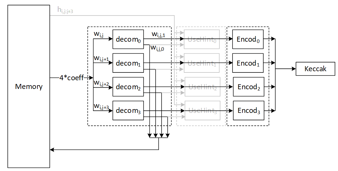
The UseHint operation in the verifying operation is as follows (with the gray components being inactive):
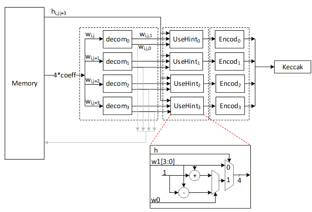
For w0 condition we have:
- if w0=0 or w0 > γ_2: w1←w1-1 mod 16
- else: w1←w1+1 mod 16
High-Level architecture
In our proposed architecture, we define specific instructions for various submodules, including SHAKE256, SHAKE128, NTT, INTT, etc. Each instruction is associated with an opcode and operands. By customizing these instructions, we can tailor the engine's behavior to different security levels.
To execute the required instructions, a high-level controller acts as a sequencer, orchestrating a precise sequence of operations. Within the architecture, several memory blocks are accessible to submodules. However, it's the sequencer's responsibility to provide the necessary memory addresses for each operation. Additionally, the sequencer handles instruction fetching, decoding, operand retrieval, and overall data flow management.
The high-level architecture of Adams Bridge controller is illustrated as follows:
Sequencer
High-Level controller works as a sequencer to perform a specific sequence of operations. There are several blocks of memory in the architecture that can be accessed by sub-modules. However, the sequencer would be responsible for passing the required addresses for each operation.
As an example, an NTT operation needs to take three base addresses as follows:
NTT(initialvalue_base_address, intermediatevalue_base_address, result_base_address)
So, for performing a=NTT(b), the sequencer needs to be:
NTT(a_base_address, temp_base_address, b_base_address)
The following table lists different operations used in the high-level controller.
Keccak and samplers Opcodes:
| Instruction | Description |
|---|---|
| RST_Keccak | Reset the Keccak SIPO buffer |
| EN_Keccak | Enable the Keccak |
| LDKeccak_MEM src, len | Load Keccak SIPO buffer at memory address src in len -width |
| LDKeccak_REG src, len | Load Keccak SIPO buffer at register ID src in len -width |
| RDKeccak_MEM dest, len | Read Keccak PISO buffer and store it at memory address dest in len -width |
| RDKeccak_REG dest, len | Read Keccak PISO buffer and store it at register ID dest in len -width |
| REJBOUND_SMPL dest | Start Keccak and RejBounded sampler and store the results at memory address dest |
| REJ_SMPL | Start Keccak and rejection sampler (results is used by PWM) |
| SMPL_INBALL | Start Keccak and SampleInBall (results is stored in SampleInBall memory) |
| EXP_MASK dest | Start Keccak and ExpandMask sampler and store the results at memory address dest |
NTT/INTT/PWO Opcodes:
| Instruction | Description |
|---|---|
| NTT src, temp, dest | Perform NTT on data at memory address src and store the results at address dest |
| INTT src, temp, dest | Perform INTT on data at memory address src and store the results at address dest |
| PWM src0, src1, dest | Perform PWM on data at memory address src0 and src1 and store the results at address dest (dest = src0*src1) |
| PWM_SMPL src, dest | Perform PWM on data from sampler and at memory address src and store the results at address dest (dest = smpl*src) |
| PWM_ACCU src0, src1, dest | Perform PWM in accumulation mode on data at memory address src0 and src1 and store the results at address dest (dest = src0*src1+dest) |
| PWM_ACCU_SMPL src, dest | Perform PWM in accumulation mode on data from sampler and at memory address src and store the results at address dest (dest = smpl*src + dest) |
| PWA src0, src1, dest | Perform PWA on data at memory address src0 and src1 and store the results at address dest (dest = src0+src1) |
| PWS src0, src1, dest | Perform PWS on data at memory src0 and src1 and store the results at address dest (dest = src0-src1) |
Other Opcodes:
| Instruction | Description |
|---|---|
| MAKEHINT src, dest | Perform MakeHint on data at memory address src and store the results at register API address dest |
| USEHINT src0, src1 | Perform Decompose on w data at memory address src0 considering the hint data at memory address src1, and perform W1Encode on w1 and store them into Keccak SIPO |
| NORM_CHK src, mode | Perform NormCheck on data at memory address src with mode configuration |
| SIG_ENCODE src0, src1, dest | Perform sigEncode on data at memory address src0 and src1 and store the results at register API address dest |
| DECOMP_SIGN src, dest | Perform Decompose on w data at memory address src and store w0 at memory address dest, and perform W1Encode on w1 and store them into Keccak SIPO |
| UPDATE_κ | The value of κ will be updated as κ+l |
| POWER2ROUND src, dest0, dest1 | Perform Power2Round on t data at memory address src and store t0 at register API address dest0 and t1 at register API address dest1 |
| SIG_DECODE_Z src, dest | Perform sigDecode_z on data at register API address src and store the results at memory address dest |
| SIG_DECODE_H src, dest | Perform sigDecode_h on data at register API address src and store the results at memory address dest |
Keygen Operation:
The algorithm for keygen is presented below. We will explain the specifics of each operation in the following subsections.
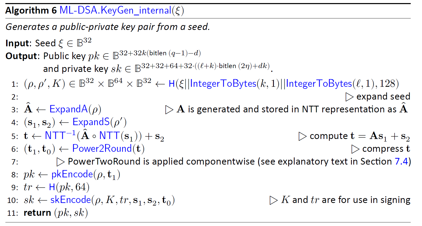
(p,p',K)= H(ξ||K||L ,1024)
Keygen starts with running Keccak operation on seed to derive three different values. Seed is a value stored in register API, and we need to perform SHAKE256 with 256-bit inputs to generate 1024 bits output.
| Operation | opcode | operand | operand | operand |
|---|---|---|---|---|
| (p,p',K)=Keccak(seed) | Keccak_SIPO | seed | 32 bytes | |
| Keccak_SIPO | K | 1 byte | ||
| Keccak_SIPO | L | 1 byte | ||
| Keccak_PISO | p | 32 bytes | ||
| Keccak_PISO | p' | 64 bytes | ||
| Keccak_PISO | K | 32 bytes |
Firstly, we need to fill Keccak input buffer with seed and then run the Keccak core. After that, the Keccak output stored in PISO is used to set the p, p’, and K values.
(s1,s2)←ExpandS(ρ′)
We use the previous step's p' as the input for the Keccak and run the rejbounded sampler. For each polynomial, we need to feed the Keccak input buffer with p' and a constant value of length 16 bits. To do this, we first feed the 512-bit p' into SIPO, and then we add a 16 bits value (which acts as a counter from 0 to 14) to the end of the fed p' and then padding starts from there.
Rejbounded opcode enables both Keccak and sampler and shows the destination of output into the memory.
Then we run the rejbounded sampler 15 times with the shake256 mode. We can mask the latency of SIPO, the Keccak_SIPO can be invoked when rejbounded is handling the previous data. However, the Keccak will not be enabled until rejbounded is done.
| Operation | opcode | operand | operand | operand |
|---|---|---|---|---|
| s1=expandS | Keccak_SIPO | p' | 0 (2bytes) | |
| rejbounded | s1_0 | |||
| Keccak_SIPO | p' | 1 | ||
| rejbounded | s1_1 | |||
| … | ||||
| Keccak_SIPO | p' | 6 | ||
| rejbounded | s1_6 | |||
| s2=expandS | Keccak_SIPO | p' | 7 | |
| rejbounded | s2_0 | |||
| … | ||||
| Keccak_SIPO | p' | 14 | ||
| rejbounded | s2_7 |
NTT(s1)
We need to call NTT for s1 by passing three addresses. Temp address can be the same for all NTT calls while init and destination are different.
| Operation | opcode | operand | operand | operand |
|---|---|---|---|---|
| NTT(s1) | NTT | s1_0 | temp | s1_0_ntt |
| NTT | s1_1 | temp | s1_1_ntt | |
| … | ||||
| NTT | s1_6 | temp | s1_6_ntt |
Aˆ ←ExpandA(ρ) AND Aˆ ◦NTT(s1)
We perform rejection sampling and PWM simultaneously. This step takes p from the first step and appends two bytes of Keccak SIPO to the end of the given p and then starts padding from there. We run the rejection sampler 56 times with shake128 mode, where k * l=56.
Each polynomial requires p and the necessary constants to fill SIPO. Then Rejection_sample opcode activates both Keccak and sampler. The output of rejection sampler goes straight to PWM unit. Then, the pwm opcode turns on pwm core, which can check the input from rejection sampler for a valid input.
There are two different opcodes for PWM: regular PWM and PWM_ACCU that indicates different modes for PWM units.
We can mask the latency of SIPO, the Keccak_SIPO can be invoked when PWM/Rejection_sampler is handling the previous data. However, the Keccak will not be enabled until PWM is done.
| Operation | opcode | operand | operand | operand |
|---|---|---|---|---|
| As1_0=PWM(A, NTT(s1)) | Keccak_SIPO | p | 0 (1 byte) | 0 (1 byte) |
| Rejection_sampler | ||||
| pwm | DONTCARE | s1_0_ntt | As0 | |
| Keccak_SIPO | p | 0 | 1 | |
| Rejection_sampler | ||||
| pwm_accu | DONTCARE | s1_1_ntt | As0 | |
| Keccak_SIPO | p | 0 | 2 | |
| Rejection_sampler | ||||
| pwm_accu | DONTCARE | s1_2_ntt | As0 | |
| … | ||||
| Keccak_SIPO | p | 0 | 6 | |
| Rejection_sampler | ||||
| pwm_accu | DONTCARE | s1_6_ntt | As0 | |
| As1_1=PWM(A, NTT(s1)) | Keccak_SIPO | p | 1 | 0 |
| Rejection_sampler | ||||
| pwm | DONTCARE | s1_0_ntt | As1 | |
| Keccak_SIPO | p | 1 | 1 | |
| Rejection_sampler | ||||
| pwm_accu | DONTCARE | s1_1_ntt | As1 | |
| … | ||||
| Keccak_SIPO | p | 1 | 6 | |
| Rejection_sampler | ||||
| pwm_accu | DONTCARE | s1_6_ntt | As1 | |
| As1_7=PWM(A, NTT(s1)) | … | |||
| Keccak_SIPO | p | 7 | 6 | |
| Rejection_sampler | ||||
| pwm_accu | DONTCARE | s1_6_ntt | As7 |
NTT−1(Aˆ ◦NTT(s1))
We need to call INTT for As1 by passing three addresses. Temp address can be the same for all INTT calls while init and destination are different.
| Operation | opcode | operand | operand | operand |
|---|---|---|---|---|
| INTT(As1) | INTT | As0 | temp | As0_intt |
| INTT | As1 | temp | As1_intt | |
| … | ||||
| INTT | As7 | temp | As7_intt |
t ←NTT−1(Aˆ ◦NTT(s1))+s2
We need to call point-wise addition for As1 results and s2 by passing three addresses.
| Operation | opcode | operand | operand | operand |
|---|---|---|---|---|
| t=INTT(As1)+s2 | PWA | As0_intt | s2_0 | t0 |
| PWA | As1_intt | s2_1 | t1 | |
| … | ||||
| PWA | As7_intt | s2_7 | t7 |
(t1,t0)←Power2Round(t,d) AND pk ←pkEncode(ρ,t1) AND sk ←skEncode(t0)
We need to call power2round for t results from the previous step, and the results are stored in two different addresses to API for sk and pk.
| Operation | Opcode | operand | operand | operand |
|---|---|---|---|---|
| (t1,t0)←Power2Round(t,d) | POWER2ROUND | t | t0 (sk) | t1 (pk) |
NOTE: The value of ρ needs to be also stored into register API for pk.
tr ←H(BytesToBits(pk),512)
The value of pk from register API needs to be read and stored into Keccak SIPO to perform SHAKE256. Due to long size of pk, 20 rounds of Keccak is required to executed to generate 512-bit tr.
| Operation | opcode | operand | operand | operand |
|---|---|---|---|---|
| tr=Keccak(pk) | Keccak_SIPO | pk | 2592 bytes | |
| Keccak_PISO | tr | 64 bytes |
sk ←skEncode(ρ,K,tr,s1,s2,t0)
The value of ρ, K needs to be stored into register API, while tr and t0 are already stored by previous steps.
We need to call skEncode for s1 and s2 coefficients and the results are stored into API for sk.
| Operation | opcode | operand | operand | operand |
|---|---|---|---|---|
| sk ←skEncode(s1) | skEncode | s1 | sk | |
| sk ←skEncode(s2) | skEncode | S2 | sk |
Signing
Signing operation is the most challenging operation for ML-DSA. From a high-level perspective, the required operation for performing a signing operation can be shown as follows:
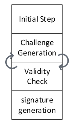
The are some initial processes to decode private key. The loop between challenge generation and validity check should be continued until validity check passed the results and then, the signature will be generated and published.
In our optimized design, the next challenge is generated in advance, so that it can be used if the validity check of the current round fails. Therefore, we use two sequencers to support parallel operations.
The algorithm for signing is presented below. We will explain the specifics of each operation in the following subsections.
The following table shows the operations for each sequencer:
| Sequencer 1 | |
|---|---|
| Challenge Generation | μ ←H(tr ||M,512) |
| ρ′←H(K||rnd||μ,512) | |
| y ←ExpandMask(ρ′ ,κ) | |
| w ←NTT−1(Aˆ ◦NTT(y)) | |
| (w1,w0) ←Decompose(w) | |
| c˜←H(μ ||w1Encode(w1),2λ) | |
| c ←SampleInBall(c˜) | |
| κ ←κ +ℓ |
| Sequencer 2 | |
|---|---|
| Initial steps | (ρ,K,tr,s1,s2,t0)←skDecode(sk) |
| sˆ1 ←NTT(s1) | |
| sˆ2 ←NTT(s2) | |
| ˆt0 ←NTT(t0) | |
| Validity Checks | cˆ ←NTT(c) |
| \⟨\⟨cs1\⟩\⟩←NTT−1(cˆ◦ sˆ1) | |
| ⟨⟨cs2⟩⟩←NTT−1(cˆ◦ sˆ2) | |
| z ←y +⟨⟨cs1⟩⟩ | |
| r0 ←(w0 −⟨⟨cs2⟩⟩) | |
| ⟨⟨ct0⟩⟩←NTT−1(cˆ◦ tˆ0) | |
| h ←MakeHint(w1, w0−⟨⟨cs2⟩⟩+⟨⟨ct0⟩⟩) | |
| ||z||∞ ≥ γ1 −β | |
| ||r0 ||∞ ≥ γ2 −β | |
| ||⟨⟨ct0⟩⟩||∞ ≥ γ2 | |
| Signature Generation | σ ←sigEncode(c˜,z mod±q,h) |
(ρ,K,tr,s1,s2,t0)←skDecode(sk)
We need to call skDecode for s1, s2, and t0 by passing the required addresses.
| Operation | opcode | operand | operand | operand |
|---|---|---|---|---|
| skDecode(s1) | skDecode | s1 | s1 | |
| skDecode(s2) | skDecode | s2 | s2 | |
| skDecode(t0) | skDecode | t0 | t0 |
sˆ1 ←NTT(s1)
We need to call NTT for s1 by passing three addresses. Temp address can be the same for all NTT calls while init and destination are different.
| Operation | opcode | operand | operand | operand |
|---|---|---|---|---|
| NTT(s1) | NTT | s1_0 | temp | s1_0_ntt |
| NTT | s1_1 | temp | s1_1_ntt | |
| … | ||||
| NTT | s1_6 | temp | s1_6_ntt |
sˆ2 ←NTT(s2)
We need to call NTT for t0 by passing three addresses. Temp address can be the same for all NTT calls while init and destination are different.
| Operation | opcode | operand | operand | operand |
|---|---|---|---|---|
| NTT(s2) | NTT | t0_0 | temp | t0_0_ntt |
| NTT | t0_1 | temp | t0_1_ntt | |
| … | ||||
| NTT | t0_7 | temp | t0_7_ntt |
ˆt0 ←NTT(t0)
We need to call NTT for s2 by passing three addresses. Temp address can be the same for all NTT calls while init and destination are different.
| Operation | opcode | operand | operand | operand |
|---|---|---|---|---|
| NTT(s2) | NTT | s2_0 | temp | s2_0_ntt |
| NTT | s2_1 | temp | s2_1_ntt | |
| … | ||||
| NTT | s2_7 | temp | s2_7_ntt |
cˆ ←NTT(c)
This is the part where two sequencers sync up. Sequencer 1 will pause until the second sequencer finishes the SampleInBall operation and the ready flag from SampleInBall tells the first sequencer to go on.
We need to call NTT for c by passing three addresses. Temp address can be the same for all NTT calls while init and destination are different.
| Operation | opcode | operand | operand | operand |
|---|---|---|---|---|
| NTT(c) | NTT | c | temp | c_ntt |
⟨⟨cs1⟩⟩←NTT−1(cˆ◦ sˆ1)
We need firstly to call PWM to perform point-wise multiplication between c and s1.
| Operation | opcode | operand | operand | operand |
|---|---|---|---|---|
| cs1=PWM(c, s1) | PWM | c_ntt | s1_0_ntt | cs1_0_ntt |
| PWM | c_ntt | s1_1_ntt | cs1_1_ntt | |
| … | ||||
| PWM | c_ntt | s1_6_ntt | cs1_6_ntt |
Then, we need to call INTT for cs1 by passing three addresses. Temp address can be the same for all INTT calls while init and destination are different.
| Operation | opcode | operand | operand | operand |
|---|---|---|---|---|
| INTT(cs1) | INTT | cs1_0_ntt | temp | cs1_0 |
| INTT | cs1_1_ntt | temp | cs1_1 | |
| … | ||||
| INTT | cs1_6_ntt | temp | cs1_6 |
⟨⟨cs2⟩⟩←NTT−1(cˆ◦ sˆ2)
We need first to call PWM to perform point-wise multiplication between c and s2.
| Operation | opcode | operand | operand | operand |
|---|---|---|---|---|
| cs2=PWM(c, s2) | PWM | c_ntt | s2_0_ntt | cs2_0_ntt |
| PWM | c_ntt | s2_1_ntt | cs2_1_ntt | |
| … | ||||
| PWM | c_ntt | s2_7_ntt | cs2_7_ntt |
Then, we need to call INTT for cs2 by passing three addresses. Temp address can be the same for all INTT calls while init and destination are different.
| Operation | opcode | operand | operand | operand |
|---|---|---|---|---|
| INTT(cs2) | INTT | cs2_0_ntt | temp | cs2_0 |
| INTT | cs2_1_ntt | temp | cs2_1 | |
| … | ||||
| INTT | cs2_7_ntt | temp | cs2_7 |
z ←y +⟨⟨cs1⟩⟩
We need to call PWA to perform point-wise addition between cs1 and y.
| Operation | opcode | operand | operand | operand |
|---|---|---|---|---|
| z=PWA(y, cs1) | PWA | y_0 | cs1_0 | z_0 |
| PWA | y_1 | cs1_1 | z_1 | |
| … | ||||
| PWA | y_6 | cs1_6 | z_6 |
r0 ←(w0 −⟨⟨cs2⟩⟩)
We need to call PWS to perform point-wise subtraction between w0 and cs2.
| Operation | opcode | operand | operand | operand |
|---|---|---|---|---|
| r0=PWS(w0, cs2) | PWS | w0_0 | cs2_0 | r0_0 |
| PWS | w0_1 | cs2_1 | r0_1 | |
| … | ||||
| PWS | w0_7 | cs2_7 | r0_7 |
⟨⟨ct0⟩⟩←NTT−1(cˆ◦ tˆ0)
We need first to call PWM to perform point-wise multiplication between c and t0.
| Operation | opcode | operand | operand | operand |
|---|---|---|---|---|
| ct0=PWM(c, t0) | PWM | c_ntt | t0_0_ntt | ct0_0_ntt |
| PWM | c_ntt | t0_1_ntt | ct0_1_ntt | |
| … | ||||
| PWM | c_ntt | t0_7_ntt | ct0_7_ntt |
Then, we need to call INTT for ct0 by passing three addresses. Temp address can be the same for all INTT calls while init and destination are different.
| Operation | opcode | operand | operand | operand |
|---|---|---|---|---|
| INTT(ct0) | INTT | ct0_0_ntt | temp | ct0_0 |
| INTT | ct0_1_ntt | temp | ct0_1 | |
| … | ||||
| INTT | ct0_7_ntt | temp | ct0_7 |
h ←MakeHint(w1,r0+⟨⟨ct0⟩⟩)
We need to call PWA to perform point-wise addition between r0 and ct0.
| Operation | opcode | operand | operand | operand |
|---|---|---|---|---|
| hint_r=PWA(r0, ct0) | PWA | hint_r_0 | r0_0 | ct0_0 |
| PWA | hint_r_1 | r0_1 | ct0_1 | |
| … | ||||
| PWA | hint_r_7 | r0_7 | ct0_7 |
Then, we need to call MakeHint for hint_r. It will process the entire hint_r polynomials, i.e., from hint_r_0 to hint_r_7.
| Operation | opcode | operand | operand | operand |
|---|---|---|---|---|
| hint_r=PWA(r0, ct0) | MAKEHINT | hint_r_0 | h |
||z||∞ ≥ γ1 −β
We need to call Norm_Check to perform validity check on z. The output will be stored as an individual flag in the high-level architecture.
| Operation | opcode | operand | operand | operand |
|---|---|---|---|---|
| Valid=NormCheck(z) | NormChk | z | mode |
||r0||∞ ≥ γ2 −β
We need to call Norm_Check to perform validity check on r0. The output will be stored as an individual flag in the high-level architecture.
| Operation | opcode | operand | operand | operand |
|---|---|---|---|---|
| Valid=NormCheck(r0) | NormChk | r | mode |
||⟨⟨ct0⟩⟩||∞ ≥ γ2
We need to call Norm_Check to perform validity check on ct0. The output will be stored as an individual flag in the high-level architecture.
| Operation | opcode | operand | operand | operand |
|---|---|---|---|---|
| Valid=NormCheck(ct0) | NormChk | ct0 | mode |
σ ←sigEncode(c˜,z mod±q,h)
This step writes the final signature into the register API. Before that, the high-level design will check all four flags coming from:
- MakeHint
- NormChk on z
- NormChk on r0
- NormChk on ct0
If all checks show the successful signature, then the sigEncode unit will be called. The value of h is already stored by MakeHint unit into the register API. Hence, only two remaining parts will be passed to this unit.
| Operation | opcode | operand | operand | operand |
|---|---|---|---|---|
| σ=sigEncode(c,z) | sigEncode | c | z | σ |
μ ←H(tr||M,512)
The other sequencer starts with running Keccak operation on tr and the given message. tr and the message are stored in register API as inputs, and we need to perform SHAKE256 with to generate 512 bits output.
| Operation | opcode | operand | operand | operand |
|---|---|---|---|---|
| μ=Keccak(tr|| M) | Keccak_SIPO | tr | 64 bytes | |
| Keccak_SIPO | 0 | 2 bytes | ||
| Keccak_SIPO | Message | 64 bytes | ||
| Keccak_PISO | μ | 64 bytes |
ρ′←H(K||rnd||μ,512)
We need to run Keccak operation on K, rnd, and μ values. K and rnd are stored in register API as inputs, and μ is stored in an internal register. we need to perform SHAKE256 with to generate 512 bits output.
| Operation | opcode | operand | operand | operand |
|---|---|---|---|---|
| ρ′=Keccak(K || rnd || μ) | Keccak_SIPO | K | 4 (x64 words) | |
| Keccak_SIPO | sign_rnd | 4 (x64 words) | ||
| Keccak_SIPO | μ | 8 (x64 words) | ||
| Keccak_PISO | ρ′ | 8 (x64 words) |
Firstly, we need to fill Keccak input buffer with K and then concatenate it with sign_rnd and μ. Then we run the Keccak core, and the Keccak output stored in PISO is used to set the ρ′ value into a special register.
y ←ExpandMask(ρ’ ,κ)
We use the previous step's p' as the input for the Keccak and run the ExpandMask sampler. For each polynomial, we need to feed the Keccak input buffer with p' and a register value of length 16 bits. To do this, we first feed the 512-bit p' into SIPO, and then we add a 16 bits value (which acts as a counter from 0 to 6) to the end of the fed p' and then padding starts from there.
ExpandMask opcode enables both Keccak and sampler and shows the destination of output into the memory.
Then we run the ExpandMask sampler 7 times with the shake256 mode. We can mask the latency of SIPO, the Keccak_SIPO can be invoked when ExpandMask is handling the previous data. However, the Keccak will not be enabled until ExpandMask is done.
| Operation | opcode | operand | operand | operand |
|---|---|---|---|---|
| y=ExpandMask(ρ’ ,κ) | LDKeccak | p' | 64 bytes | |
| LDKeccak | κ | 2 bytes | ||
| Exp_Mask | y_0 | |||
| LDKeccak | p' | 1 bytes | ||
| LDKeccak | κ+1 | 2 bytes | ||
| Exp_Mask | y_1 | |||
| … | ||||
| LDKeccak | p' | 64 bytes | ||
| LDKeccak | κ +6 | 2 bytes | ||
| Exp_Mask | y_6 |
NTT(y)
We need to call NTT for s1 by passing three addresses. Temp address can be the same for all NTT calls while init and destination are different.
| Operation | opcode | operand | operand | operand |
|---|---|---|---|---|
| NTT(y) | NTT | y_0 | temp | y_0_ntt |
| NTT | y_1 | temp | y_1_ntt | |
| … | ||||
| NTT | y_6 | temp | y_6_ntt |
Aˆ ←ExpandA(ρ) AND Aˆ ◦NTT(y)
We perform rejection sampling and PWM simultaneously. This step takes p from and appends two bytes of Keccak SIPO to the end of the given p and then starts padding from there. We run the rejection sampler 56 times with shake128 mode, where k * l=56.
Each polynomial requires p and the necessary constants to fill SIPO. Then Rejection_sample opcode activates both Keccak and sampler. The output of rejection sampler goes straight to PWM unit. Then, the pwm opcode turns on pwm core, which can check the input from rejection sampler for a valid input.
There are two different opcodes for PWM: regular PWM and PWM_ACCU that indicates different modes for PWM units.
We can mask the latency of SIPO, the Keccak_SIPO can be invoked when PWM/Rejection_sampler is handling the previous data. However, the Keccak will not be enabled until PWM is done.
| Operation | opcode | operand | operand | operand |
|---|---|---|---|---|
| Ay0=PWM(A, NTT(y)) | LDKeccak | p | 32 bytes | |
| LDKeccak | 0 | 1 byte | ||
| LDKeccak | 0 | 1 byte | ||
| Rejection_sampler | ||||
| pwm | DONTCARE | y_0_ntt | Ay0 | |
| LDKeccak | p | 32 bytes | ||
| LDKeccak | 0 | 1 byte | ||
| LDKeccak | 1 | 1 byte | ||
| Rejection_sampler | ||||
| pwm_accu | DONTCARE | y_1_ntt | Ay0 | |
| LDKeccak | p | 32 bytes | ||
| LDKeccak | 0 | 1 byte | ||
| LDKeccak | 2 | 1 byte | ||
| Rejection_sampler | ||||
| pwm_accu | DONTCARE | y_2_ntt | Ay0 | |
| … | ||||
| LDKeccak | p | 32 bytes | ||
| LDKeccak | 0 | 1 byte | ||
| LDKeccak | 6 | 1 byte | ||
| Rejection_sampler | ||||
| pwm_accu | DONTCARE | y_6_ntt | Ay0 | |
| Ay1=PWM(A, NTT(y)) | LDKeccak | p | 32 bytes | 0 |
| LDKeccak | 1 | 1 byte | ||
| LDKeccak | 0 | 1 byte | ||
| Rejection_sampler | ||||
| pwm | DONTCARE | y_0_ntt | Ay1 | |
| LDKeccak | p | 32 bytes | ||
| LDKeccak | 1 | 1 byte | ||
| LDKeccak | 1 | 1 byte | ||
| Rejection_sampler | ||||
| pwm_accu | DONTCARE | y_1_ntt | Ay1 | |
| … | ||||
| LDKeccak | p | 32 bytes | ||
| LDKeccak | 1 | 1 byte | ||
| LDKeccak | 6 | 1 byte | ||
| Rejection_sampler | ||||
| pwm_accu | DONTCARE | y_6_ntt | Ay1 | |
| Ay7=PWM(A, NTT(y)) | … | |||
| LDKeccak | p | 32 bytes | ||
| LDKeccak | 7 | 1 byte | ||
| LDKeccak | 6 | 1 byte | ||
| Rejection_sampler | ||||
| pwm_accu | DONTCARE | y_6_ntt | Ay7 |
w ←NTT−1(Aˆ ◦NTT(y))
We need to call INTT for Ay by passing three addresses. Temp address can be the same for all INTT calls while init and destination are different.
| Operation | opcode | operand | operand | operand |
|---|---|---|---|---|
| INTT(Ay) | INTT | Ay0 | temp | w_0 |
| INTT | Ay1 | temp | w_1 | |
| … | ||||
| INTT | Ay7 | temp | w_7 |
(w1,w0) ←Decompose(w) AND c˜←H(μ||w1Encode(w1),2λ)
The decompose unit takes w from memory and splits it into two parts. It saves w0 in memory and sends w1 to the Keccak SIPO for SampleInBall. However, SIPO requires the μ prefix before receiving the w1 values. Therefore, the high-level controller should provide μ before using decompose. After completing the decompose operation, the high-level controller needs to add the necessary padding for H(μ||w1Encode(w1),2λ). Then, by activating the SampleInBall, the Keccak will start and the data in the SIPO will be processed.
| Operation | opcode | operand | operand | operand |
|---|---|---|---|---|
| H(μ || w1Encode(w1),2λ) | LDKeccak | μ | 64 bytes | |
| (w1,w0) ←Decompose(w) | Decomp_Enc | w | w0 | |
| H(μ | w1Encode(w1),2λ) | LDKeccak | padding |
c ←SampleInBall(c˜)
We take the SIPO value from the last step as the Keccak input and run SampleInBall. The output stays in the SampleInBall memory.
| Operation | opcode | operand | operand | operand |
|---|---|---|---|---|
| c ←SampleInBall(c˜1) | SMPL_INBALL |
κ ←κ +ℓ
High-level controller increases the value of κ by l.
| Operation | opcode | operand | operand | operand |
|---|---|---|---|---|
| κ ←κ +ℓ | Update_k |
Verifying
The algorithm for verifying is presented below. We will explain the specifics of each operation in the following subsections.
(ρ,t1)←pkDecode(pk)
We need to call pkDecode to decode the given pk for t1 values.
| Operation | opcode | operand | operand | operand |
|---|---|---|---|---|
| t1←pkDecode(pk) | pkDecode | pk | t1 |
(c˜,z,h)←sigDecode(σ)
We need to call sigDecode to decode the given signature for z and h values.
| Operation | opcode | operand | operand | operand |
|---|---|---|---|---|
| (z,h)←sigDecode(σ) | sigDecode_z | σ_z | z | |
| sigDecode_h | σ_h | h |
||z||∞ ≥ γ1 −β
We need to call Norm_Check to perform validity check on the given z. The output will be stored as an individual flag in the high-level architecture.
| Operation | opcode | operand | operand | operand |
|---|---|---|---|---|
| Valid=NormCheck(z) | NormChk | z | mode |
[[number of 1’s in h is ≤ ω]]
We need to call HintSum to perform validity check on the given h. The output will be stored as an individual flag in the high-level architecture.
| Operation | opcode | operand | operand | operand |
|---|---|---|---|---|
| Valid=HintSum(h) | HINTSUM | h |
z ←NTT(z)
We need to call NTT for z by passing three addresses. Temp address can be the same for all NTT calls while init and destination are different.
| Operation | opcode | operand | operand | operand |
|---|---|---|---|---|
| NTT(z) | NTT | z_0 | temp | z_0_ntt |
| NTT | z_1 | temp | z_1_ntt | |
| … | ||||
| NTT | z_6 | temp | z_6_ntt |
Aˆ ←ExpandA(ρ) AND Aˆ ◦NTT(z)
We perform rejection sampling and PWM simultaneously. This step takes p from the register API and appends two bytes of Keccak SIPO to the end of the given p and then starts padding from there. We run the rejection sampler 56 times with shake128 mode, where k * l=56.
Each polynomial requires p and the necessary constants to fill SIPO. Then Rejection_sample opcode activates both Keccak and sampler. The output of rejection sampler goes straight to PWM unit. Then, the pwm opcode turns on pwm core, which can check the input from rejection sampler for a valid input.
There are two different opcodes for PWM: regular PWM and PWM_ACCU that indicates different modes for PWM units.
We can mask the latency of SIPO, the Keccak_SIPO can be invoked when PWM/Rejection_sampler is handling the previous data. However, the Keccak will not be enabled until PWM is done.
| Operation | opcode | operand | operand | operand |
|---|---|---|---|---|
| Az_0=PWM(A, NTT(z)) | Keccak_SIPO | p | 0 (1 byte) | 0 (1 byte) |
| Rejection_sampler | ||||
| pwm | DONTCARE | z_0_ntt | Az0 | |
| Keccak_SIPO | p | 0 | 1 | |
| Rejection_sampler | ||||
| pwm_accu | DONTCARE | z_1_ntt | Az0 | |
| Keccak_SIPO | p | 0 | 2 | |
| Rejection_sampler | ||||
| pwm_accu | DONTCARE | z_2_ntt | Az0 | |
| … | ||||
| Keccak_SIPO | p | 0 | 6 | |
| Rejection_sampler | ||||
| pwm_accu | DONTCARE | z_6_ntt | Az0 | |
| Az_1=PWM(A, NTT(z)) | Keccak_SIPO | p | 1 | 0 |
| Rejection_sampler | ||||
| pwm | DONTCARE | z_0_ntt | Az1 | |
| Keccak_SIPO | p | 1 | 1 | |
| Rejection_sampler | ||||
| pwm_accu | DONTCARE | z_1_ntt | Az1 | |
| … | ||||
| Keccak_SIPO | p | 1 | 6 | |
| Rejection_sampler | ||||
| pwm_accu | DONTCARE | z_6_ntt | Az1 | |
| Az_7=PWM(A, NTT(z)) | … | |||
| Keccak_SIPO | p | 7 | 6 | |
| Rejection_sampler | ||||
| pwm_accu | DONTCARE | z_6_ntt | Az7 |
tr ←H(pk,512)
The sequencer runs Keccak operation on pk. pk is stored in register API as input, and we need to perform SHAKE256 with to generate 512 bits output.
| Operation | opcode | operand | operand | operand |
|---|---|---|---|---|
| tr=Keccak(pk) | Keccak_SIPO | pk | 2592 bytes | |
| Keccak_PISO | tr | 64 bytes |
μ ←H(tr||M,512)
The sequencer starts with running Keccak operation on tr and the given message. tr is stored in an internal register from the previous step, and the message is stored in register API as input, and we need to perform SHAKE256 with to generate 512 bits output.
| Operation | opcode | operand | operand | operand |
|---|---|---|---|---|
| μ=Keccak(tr || M) | Keccak_SIPO | tr | 64 bytes | |
| Keccak_SIPO | 0 | 2 bytes | ||
| Keccak_SIPO | Message | 64 bytes | ||
| Keccak_PISO | μ | 64 bytes |
c ←SampleInBall(c˜)
We take the c~ values from register API as the Keccak input and run SampleInBall. The output stays in the SampleInBall memory.
| Operation | opcode | operand | operand | operand |
|---|---|---|---|---|
| Keccak_SIPO | c~ | 64 bytes | ||
| c ←SampleInBall(c˜) | SMPL_INBALL |
cˆ ←NTT(c)
We need to call NTT for c by passing three addresses. Temp address can be the same for all NTT calls while init and destination are different.
| Operation | opcode | operand | operand | operand |
|---|---|---|---|---|
| NTT(c) | NTT | c | temp | c_ntt |
cˆ ←NTT(c)
We need to call NTT for c by passing three addresses. Temp address can be the same for all NTT calls while init and destination are different.
| Operation | opcode | operand | operand | operand |
|---|---|---|---|---|
| NTT(c) | NTT | c | temp | c_ntt |
t1 ←NTT(t1)
We need to call NTT for t1 by passing three addresses. Temp address can be the same for all NTT calls while init and destination are different.
| Operation | opcode | operand | operand | operand |
|---|---|---|---|---|
| NTT(t1) | NTT | t1_0 | temp | t1_0_ntt |
| NTT | t1_1 | temp | t1_1_ntt | |
| … | ||||
| NTT | t1_7 | temp | t1_7_ntt |
NTT(c) ◦NTT(t1)
We need to call point-wise multiplication between c and all t1 polynomials in NTT domain.
| Operation | opcode | operand | operand | operand |
|---|---|---|---|---|
| ct1=PWM(NTT(c) ◦NTT(t1)) | PWM | c_ntt | t1_0_ntt | ct1_0 |
| PWM | c_ntt | t1_1_ntt | ct1_1 | |
| … | ||||
| . | PWM | c_ntt | t1_7_ntt | ct1_7 |
A ˆ ◦NTT(z*)* −NTT(c) ◦NTT(t1)
We need to call point-wise subtraction between Az and ct1 polynomials in NTT domain.
| Operation | opcode | operand | operand | operand |
|---|---|---|---|---|
| Az-ct1=A ˆ ◦NTT(z*)* −NTT(c) ◦NTT(t1) | PWS | Az_0 | ct1_0 | Az_ct1_0 |
| PWS | Az_1 | ct1_1 | Az_ct1_1 | |
| … | ||||
| . | PWS | Az_7 | ct1_7 | Az_ct1_7 |
w′ ←NTT-1(A ˆ ◦NTT(z*)* −NTT(c) ◦NTT(t1))
We need to call INTT for Az_ct1 by passing three addresses. Temp address can be the same for all INTT calls while init and destination are different.
| Operation | opcode | operand | operand | operand |
|---|---|---|---|---|
| w′ ←NTT-1(A ˆ ◦NTT(z*)* −NTT(c) ◦NTT(t1)) | INTT | Az_ct1_0 | temp | w’_0 |
| INTT | Az_ct1_1 | temp | w’_1 | |
| … | ||||
| INTT | Az_ct1_7 | temp | w’_7 |
w ′ ←UseHint(h,w ′) AND c˜←H(μ||w1Encode(w1),2λ)
In the UseHint phase, the decompose unit retrieves w from memory and divides it into two components. Next, w1 is refreshed through useHint, encoded, and forwarded to the Keccak SIPO. Nonetheless, the μ prefix must precede w1 before SIPO can accept it. Therefore, the high-level controller should provide μ before using decompose. After completing the UseHint operation, the high-level controller needs to add the necessary padding for H(μ||w1Encode(w1),2λ). Then, the Keccak will start and the data in the SIPO will be stored at register API as verification result.
| Operation | opcode | operand | operand | operand |
|---|---|---|---|---|
| H(μ || w1Encode(w1),2λ) | LDKeccak | μ | 64 bytes | |
| w ′ ←UseHint(h,w ′) | USEHINT | w | H | |
| H(μ || w1Encode(w1),2λ) | LDKeccak | padding | ||
| EN_Keccak | ||||
| RDKeccak | Verification Result |
MLDSA Memory Layout (Unmasked, MASKING_EN=0)
When
MASKING_EN = 1, eachinst0_bank0/inst0_bank1/inst1/inst2instance below has a same-dimension mirror instance with the_maskedsuffix that holdsshare1of the same coefficient set; the regular instances holdshare0. The offset tables apply to both. Seeabr_mem_top.svfor the gated instantiation.
Memory Instances
| Instance | Type | Depth | Width | Size |
|---|---|---|---|---|
| inst0 | Banked (2 banks) | 800/bank (1600 total) | 96-bit | 18.75 KB |
| inst1 | Single | 64 | 96-bit | 0.75 KB |
| inst2 | Single | 1536 | 96-bit | 18 KB |
| SIB | Single | - | - | SampleInBall |
Address scheme: top 3 bits select instance (0=inst0, 1=inst1, 2=inst2, 4=SIB). inst0 bit[0] selects bank. All memories are 1R1W.
KeyGen Memory Layout
inst0 (KeyGen)
| Offset | Entries | Name | Notes |
|---|---|---|---|
| 0- 447 | 448 | S1_0..S1_6 | ExpandS output, 7x64 |
| 448- 959 | 512 | S2_0..S2_7 | ExpandS output, 8x64 |
| 960-1471 | 512 | T0..T7 | A*s1+s2 result, 8x64 |
| 1536-1599 | 64 | TEMP0 | NTT scratch |
inst1 (KeyGen)
| Offset | Entries | Name | Notes |
|---|---|---|---|
| 0- 63 | 64 | AS0 / AS0_INTT | A*NTT(s1) accumulator, reused per row |
inst2 (KeyGen)
| Offset | Entries | Name | Notes |
|---|---|---|---|
| 64- 511 | 448 | S1_0_NTT..S1_6_NTT | NTT(s1) for ExpandA, 7x64 |
| 1472-1535 | 64 | TEMP2 | INTT scratch |
KeyGen Data Flow
1. ExpandS -> S1[0..6], S2[0..7]                      (inst0)
2. NTT(S1_i) -> S1_i_NTT                              (inst0 -> inst2, temp: inst0/TEMP0)
3. For each row i=0..7:
   a. ExpandA x S1_NTT -> AS0                          (inst2 read, inst1 write)
   b. INTT(AS0) -> AS0_INTT                            (inst1 in-place, temp: inst2/TEMP2)
   c. AS0_INTT + S2_i -> T_i                           (inst1 read + inst0 read -> inst0 write)
4. Power2Round(T) -> t1,t0                             (inst0 read)
5. skEncode(S1, S2, T0)                                (inst0 read)
Signing Memory Layout
inst0 (Signing)
| Offset | Entries | Name | Notes |
|---|---|---|---|
| 0- 447 | 448 | S1_0..S1_6 | NTT(s1) from skDecode, 7x64 |
| 448- 959 | 512 | S2_0..S2_7 | NTT(s2) from skDecode, 8x64 |
| 960-1471 | 512 | T0..T7 | NTT(t) from skDecode, 8x64 |
| 1472-1535 | 64 | CS1/Z/CS2/R0/AY0/CS_NTT/CT_NTT | Shared scratch (sequential reuse) |
| 1536-1599 | 64 | TEMP0 | NTT scratch |
inst1 (Signing)
| Offset | Entries | Name | Notes |
|---|---|---|---|
| 0- 63 | 64 | C_NTT | NTT(c) from SampleInBall |
inst2 (Signing)
| Offset | Entries | Name | Notes |
|---|---|---|---|
| 0- 447 | 448 | Y_0..Y_6 | ExpandMask output, 7x64 |
| 448- 959 | 512 | Y_NTT / CT_0..CT_7 / HINT_R_0..HINT_R_7 | NTT(Y) then reused for c*t and hints, 8x64 |
| 960-1471 | 512 | W0_0..W0_7 | INTT(A*Y) decompose input, 8x64 |
| 1472-1535 | 64 | TEMP2 | INTT scratch |
Signing Data Flow
1. skDecode -> NTT(S1), NTT(S2), NTT(T)               (inst0)
2. ExpandMask -> Y[0..6]                               (inst2)
3. NTT(Y_i) -> Y_i_NTT                                (inst2 in-place, temp: inst2/TEMP2)
4. For each row i=0..7:
   a. ExpandA x Y_NTT -> AY0                           (inst2 read -> inst0/1472 write)
   b. INTT(AY0) -> W0_i                                (inst0 read -> inst2 write, temp: inst2/TEMP2)
5. Decompose(W0) -> w1, w0                             (inst2 read/write)
6. NTT(c) -> C_NTT                                     (SIB -> inst1)
7. For each i=0..6:
   a. C_NTT x S1_i -> CS_NTT                           (inst1 x inst0 -> inst0/1472)
   b. INTT(CS_NTT) -> CS1                              (inst0 in-place, temp: inst2/TEMP2)
   c. Y_i + CS1 -> Z                                   (inst2 + inst0 -> inst0/1472)
   d. NormCheck(Z), SigEncode(Z)
8. For each i=0..7:
   a. C_NTT x T_i -> CT_NTT                            (inst1 x inst0 -> inst0/1472)
   b. INTT(CT_NTT) -> CT_i                             (inst0 -> inst2, temp: inst2/TEMP2)
9. For each i=0..7:
   a. C_NTT x S2_i -> CS_NTT                           (inst1 x inst0 -> inst0/1472)
   b. INTT(CS_NTT) -> CS2                              (inst0 in-place, temp: inst2/TEMP2)
   c. W0_i - CS2 -> R0                                 (inst2 - inst0 -> inst0/1472)
   d. R0 + CT_i -> HINT_R_i                            (inst0 + inst2 -> inst2)
10. MakeHint(HINT_R)                                    (inst2 read)
Verify Memory Layout
inst0 (Verify)
| Offset | Entries | Name | Notes |
|---|---|---|---|
| 0- 447 | 448 | Z_0..Z_6 / Z_NTT_0..Z_NTT_6 | sigDecode_z output, NTT in-place, 7x64 |
| 448- 959 | 512 | HINT_R (verify) | sigDecode_h output, aliases S2 region, 8x64 |
| 960-1471 | 512 | T0..T7 | pkDecode output, NTT in-place, 8x64 |
| 1472-1535 | 64 | CT_v | C_NTT x T_i scratch |
| 1536-1599 | 64 | TEMP0 | NTT scratch |
inst1 (Verify)
| Offset | Entries | Name | Notes |
|---|---|---|---|
| 0- 63 | 64 | C_NTT | NTT(c) from SampleInBall |
inst2 (Verify)
| Offset | Entries | Name | Notes |
|---|---|---|---|
| 448- 959 | 512 | AZ0 | A*z accumulator, aliases HINT_R/CT signing slots, 8x64 |
| 960-1471 | 512 | W0_0..W0_7 | Az-ct result, 8x64 |
Verify Data Flow
1. pkDecode -> T0..T7                                  (inst0)
2. sigDecode_z -> Z_0..Z_6                             (inst0, aliases S1 slots)
3. NormCheck(Z)
4. NTT(T_i) in-place                                   (inst0, temp: inst0/TEMP0)
5. NTT(Z_i) -> Z_NTT_i in-place                       (inst0, temp: inst0/TEMP0)
6. NTT(c) -> C_NTT                                     (SIB -> inst1)
7. For each row i=0..7:
   a. ExpandA x Z_NTT -> AZ0                           (inst0 read -> inst2/448 write)
   b. C_NTT x T_i -> CT_v                              (inst1 x inst0 -> inst0/1472)
   c. CT_v - AZ0 -> AZ0                                (inst0 - inst2 -> inst2 in-place)
   d. INTT(AZ0) -> W0_i                                (inst2 -> inst2, temp: inst0/TEMP0)
8. sigDecode_h -> HINT_R                                (inst0/448, aliases S2)
9. UseHint(W0, HINT_R) -> w1                           (inst2 read W0, inst0 read HINT_R)
References:
[1] The White House, "National Security Memorandum on Promoting United States Leadership in Quantum Computing While Mitigating Risks to Vulnerable Cryptographic Systems," 2022. [Online]. Available: White House.
[2] NIST, "PQC Standardization Process: Announcing Four Candidates to be Standardized, Plus Fourth Round Candidates," [Online]. Available: NIST PQC. [Accessed 2022].
[3] NIST, "FIPS 204 Module-Lattice-Based Digital Signature Standard," August 13, 2024.
96cdd1d
![]()
Adam's Bridge ML-KEM Hardware Specification
Version 1.0
ML-KEM Overview
ML-KEM (Module-Lattice-Based Key-Encapsulation Mechanism) is a quantum-resistant Key exchange scheme defined in FIPS 203 [1].
High-Level Overview
Adam’s Bridge MK-KEM accelerator has all the necessary components to execute a pure hardware PQC operation. The main operations that involve more computational complexity, such as NTT, hashing, and sampling units, are explained as follows.
The security level of ML-KEM defined by NIST are as follows:
| Algorithm Name | Security Level |
|---|---|
| ML-KEM-512 | Level-1 |
| ML-KEM-768 | Level-3 |
| ML-KEM-1024 | Level-5 |
CNSA 2.0 only allows the highest security level (Level-5) for PQC which is ML-KEM-1024, and Adams Bridge only supports ML-KEM-1024 parameter set.
API
The ML-KEM-1024 architecture inputs and outputs are described in the following table.
| Name | Input/Output | Operation | Size (Byte) |
|---|---|---|---|
| name | Output | All | 8 |
| version | Output | All | 8 |
| ctrl | Input | All | 4 |
| status | Output | All | 4 |
| entropy (SCA) | Input | All | 64 |
| seed_d | Input | Keygen | 32 |
| seed_z | Input | Keygen | 32 |
| message | Input | Encaps | 32 |
| shared_key | Output | Encaps/Decaps | 32 |
| decaps_key | Input/Output | Keygen/Decaps | 3168 |
| encaps_key | Input/Output | Keygen/Decaps | 1568 |
| ciphertext | Input/Output | Encaps/Decaps | 1568 |
| Interrupt | Output | All | 520 |
| --------------------------- | --------------- | --------------- | ------------- |
| Total | 7040 |
name
Read-only register consists of the name of component.
version
Read-only register consists of the version of component.
CTRL
The control register consists of the following flags:
| Bits | Identifier | Access | Reset | Decoded | Name |
|---|---|---|---|---|---|
| [31:4] | - | - | - | - | |
| [3] | ZEROIZE | w | 0x0 | - | |
| [2:0] | CTRL | w | 0x0 | - |
CTRL
CTRL command field contains two bits indicating:
- Ctrl = 0b000
No Operation.
- Ctrl = 0b001
Trigs the core to start the initialization and perform keygen operation.
- Ctrl = 0b010
Trigs the core to start the Encapsulation operation.
- Ctrl = 0b011
Trigs the core to start Decapsulation operation.
- Ctrl = 0b100
Trigs the core to start the keygen+Decapsulation operation for a ciphertext block. This mode decreases storage costs for the decaps_key (dk) by recalling keygen and using an on-the-fly decaps_key during the decapsultion process.
ZEROIZE
Clears all internal data-path registers holding secret-derived values. See the Zeroize section in the top-level specification for the full zeroize policy.
status
The read-only status register consists of the following flags:
| Bits | Identifier | Access | Reset | Decoded | Name |
|---|---|---|---|---|---|
| [31:3] | - | - | - | - | |
| [2] | ERROR | r | 0x0 | - | |
| [1] | VALID | r | 0x0 | - | |
| [0] | READY | r | 0x0 | - |
READY
Indicates if the core is ready to process the inputs.
VALID
Indicates if the process is computed and the output is valid.
ERROR
Indicates if the process could not complete due to an error. For encapsulation, this indicates that the provided encapsulation key does not pass the FIPS 203 input check (Modulus check). For decapsulation, this indicates that the provided decapsulation key does not pass the FIPS 203 input check (Hash check).
entropy
Entropy is required for SCA countermeasures to randomize the inputs with no change in the outputs. The entropy can be any 512-bit value in [0 : 2^512-1].
The ML-KEM-1024 countermeasure requires several random vectors to randomize the intermediate values. An internal mechanism is considered to take one random vector of 512-bit (i.e., entropy register) and generate the required random vectors for different countermeasures.
seed_d
Adams Bridge component seed_d register type definition 8 32-bit registers storing the 256-bit seed_d for keygen. The seed can be any 256-bit value in [0 : 2^256-1].
seed_z
Adams Bridge component seed_z register type definition 8 32-bit registers storing the 256-bit seed_z for keygen. The seed can be any 256-bit value in [0 : 2^256-1].
message
Adams Bridge component message register type definition 8 32-bit registers storing the 256-bit message for encapsulation. The message can be any 256-bit value in [0 : 2^256-1].
shared_key
This register stores the shared_key for generated by encapsulation or decapsulation operations.
decaps_key
This register stores the decapsulation key generated in keygen. This register should be set before decapsulation operation.
If seed_d or seed_z comes from key vault, this register will not contain the decaps_key to avoid exposing secret assets to software.
encaps_key
This register stores the encapsulation key generated in keygen. This register should be set before encapsulation operation.
ciphertext
This register stores the ciphertext generated in encapsulation operation. This register should be set before decapsulation operation.
Endianness and byte ordering
All ML-KEM registers use little-endian byte ordering within each 32-bit register. Byte 0 of an algorithm input or output occupies bits [7:0] of register index 0, byte 1 occupies bits [15:8], and so on. Firmware writes FIPS 203 byte arrays directly to registers with no byte swapping or DWORD reordering: byte[0] maps to register[0][7:0].
For Key Vault byte ordering and DWORD reversal details, see the Key Vault endianness and byte ordering section in CaliptraHardwareSpecification.md.
Pseudocode
Keygen
Input:
    seed_d
    seed_z
    entropy

Output:
    encaps_key
    decaps_key

// Wait for the core to be ready (STATUS flag should be 2'b01, i.e., READY=1, VALID=0)
read_data = 0
while read_data == 0:
    read_data = read(ADDR_STATUS)

// Feed the required inputs
write(ADDR_SEED_D, seed_d)
write(ADDR_SEED_Z, seed_z)
write(ADDR_ENTROPY, entropy)

// Trigger the core for performing Keygen
write(ADDR_CTRL, KEYGEN_CMD)  // (STATUS flag will be changed to 2'b00)

// Wait for the operation to complete (STATUS flag should be 2'b10, i.e., READY=0, VALID=1).
read_data = 0
while read_data == 0:
    read_data = read(ADDR_STATUS)

// Reading the outputs
encaps_key = read(ADDR_EK)
decaps_key = read(ADDR_DK)

// Zeroize (mandatory after every completed operation)
write(ADDR_CTRL, ZEROIZE_CMD)
// Wait for the core to be ready again (STATUS flag should be 2'b01)
read_data = 0
while read_data == 0:
    read_data = read(ADDR_STATUS)

// Return the outputs
return encaps_key, decaps_key
Encapsulation
Input:
msg
encaps_key
entropy
Output:
shared_key
ciphertext
// Wait for the core to be ready (STATUS flag should be 2'b01, i.e., READY=1, VALID=0)
read_data = 0;
while (read_data == 0) {
read_data = read(ADDR_STATUS);
}
// Feed the required inputs
write(ADDR_MSG, msg);
write(ADDR_EK, encaps_key);
write(ADDR_ENTROPY, entropy);
// Trigger the core for performing Encapsulation
write(ADDR_CTRL, ENCAPS_CMD); // (STATUS flag will be changed to 2'b00)
// Wait for the operation to complete (STATUS flag should be 2'b10, i.e., READY=0, VALID=1).
read_data = 0;
while (read_data == 0) {
read_data = read(ADDR_STATUS);
}
// Reading the outputs
shared_key = read(ADDR_SHAREDKEY);
ciphertext = read(ADDR_CIPHERTEXT);
// Zeroize (mandatory after every completed operation)
write(ADDR_CTRL, ZEROIZE_CMD);
// Wait for the core to be ready again (STATUS flag should be 2'b01)
read_data = 0;
while (read_data == 0) {
read_data = read(ADDR_STATUS);
}
// Return the output
return shared_key, ciphertext;
Decapsulation
Input:
    decaps_key
    ciphertext
    entropy

Output:
    shared_key

// Wait for the core to be ready (STATUS flag should be 2'b01, i.e., READY=1, VALID=0)
read_data = 0;
while (read_data == 0) {
    read_data = read(ADDR_STATUS);
}

// Feed the required inputs
write(ADDR_DK, decaps_key);
write(ADDR_CIPHERTEXT, ciphertext);
write(ADDR_ENTROPY, entropy);

// Trigger the core for performing decapsulation
write(ADDR_CTRL, DECAPS_CMD);  // (STATUS flag will be changed to 2'b00)

// Wait for the operation to complete (STATUS flag should be 2'b10, i.e., READY=0, VALID=1).
read_data = 0;
while (read_data == 0) {
    read_data = read(ADDR_STATUS);
}

// Reading the output
shared_key = read(ADDR_SHAREDKEY);

// Zeroize (mandatory after every completed operation)
write(ADDR_CTRL, ZEROIZE_CMD);
// Wait for the core to be ready again (STATUS flag should be 2'b01)
read_data = 0;
while (read_data == 0) {
    read_data = read(ADDR_STATUS);
}

// Return the output
return shared_key;
Keygen + Decapsulation
This mode decreases storage costs for the decaps_key (DK) by recalling keygen and using an on-the-fly decaps_key during the decapsulaiton process.
Input:
    seed_d
    seed_z
    ciphertext
    entropy

Output:
    shared_key

// Wait for the core to be ready (STATUS flag should be 2'b01, i.e., READY=1, VALID=0)
read_data = 0
while read_data == 0:
    read_data = read(ADDR_STATUS)

// Feed the required inputs
write(ADDR_SEED_D, seed_d)
write(ADDR_SEED_Z, seed_z)
write(ADDR_CIPHERTEXT, ciphertext);
write(ADDR_ENTROPY, entropy)

// Trigger the core for performing Keygen + Decapsulation
write(ADDR_CTRL, KEYGEN_DECAPS_CMD)  // (STATUS flag will be changed to 2'b00)

// Wait for the operation to complete (STATUS flag should be 2'b10, i.e., READY=0, VALID=1).
read_data = 0
while read_data == 0:
    read_data = read(ADDR_STATUS)

// Reading the output
shared_key = read(ADDR_SHAREDKEY);

// Zeroize (mandatory after every completed operation)
write(ADDR_CTRL, ZEROIZE_CMD);
// Wait for the core to be ready again (STATUS flag should be 2'b01)
read_data = 0;
while (read_data == 0) {
    read_data = read(ADDR_STATUS);
}

// Return the outputs
return shared_key;
Performance and Area Results
ML-KEM-1024
The performance results for two operational frequencies, 400 MHz and 600 MHz, are presented in terms of latency (clock cycles [CCs]), time [ms], and performance [IOPS] as follows:
| Freq [MHz] | 400 | 600 | ||||
|---|---|---|---|---|---|---|
| "Unprotected" | Latency [CC] | Time [ms] | Performance [IOPS] | Time [ms] | Performance [IOPS] | |
| Key Generation | 6,640 | 0.017 | 60,241 | 0.011 | 90,361 | |
| Encapsulation | 7,930 | 0.020 | 50,441 | 0.013 | 75,662 | |
| Decapsulation | 11,054 | 0.028 | 36,186 | 0.018 | 54,279 |
NOTE: Masking countermeasures are implemented at the architectural level: shares are produced by abr_splitter.sv, processed by two parallel NTT engines (NTT[0] on share0, NTT[1] on share1), and recombined inline at each unmasked consumer via the shared abr_recombiner.sv primitive. The build-time MASKING_EN parameter selects between the protected (MASKING_EN=1) and unprotected (MASKING_EN=0) configurations at elaboration. See AdamsBridgeSCA.md for the side-channel countermeasure overview.
Masking imposes zero cycle overhead. The only cost of enabling masking is area:
| Freq [MHz] | 400 | 600 | ||||
|---|---|---|---|---|---|---|
| "Protected" | Latency [CC] | Time [ms] | Performance [IOPS] | Time [ms] | Performance [IOPS] | |
| Key Generation | 6,640 | 0.017 | 60,241 | 0.011 | 90,361 | |
| Encapsulation | 7,930 | 0.020 | 50,441 | 0.013 | 75,662 | |
| Decapsulation | 11,056 | 0.028 | 36,179 | 0.018 | 54,269 |
- CNSA 2.0 only allows the highest security level (Level-5) for PQC which is ML-KEM-1024, and Adams Bridge only supports ML-KEM-1024 parameter set.
- For total Adams Bridge area results, see the Area Results section in AdamsBridgeHardwareSpecification.md.
- The design is converging today at 600MHz at low, med & high voltage corners. (We have noticed the design converging to 1 GHz on a latest process node.)
NTT/INTT
Number Theoretic Transform (NTT) and inverse Number Theoretic Transform (INTT) are used to achieve more efficient polynomial multiplication in lattice-based cryptosystems by reducing time-complexity from O(n2) to O(n log n).
NTT/INTT computation is made up of many butterfly operations. A butterfly operation is a mathematical operation that merges two coefficients to produce two outputs to help with NTT and INTT calculation. The NTT engine consists of 2 stages of 2 butterfly units connected serially which results in a 2x2 architecture. This is a pipelined architecture where every clock cycle, each butterfly unit receives two input coefficients and produces two output coefficients.
As a result of this pipelined 2x2 architecture, even number of stages are executed to complete a single NTT/INTT operation. However, in ML-KEM definition of NTT/INTT, (log n)-1 layers of NTT operation must be performed, where n is the number of coefficients in the polynomial. For n = 256, 7 layers of computation must be done to complete one NTT/INTT operation.
This mismatch between the required odd number of layers in ML-KEM and the fixed even-layered execution of a conventional pipelined NTT/INTT engine creates a fundamental challenge. ML-KEM employs an even/odd coefficient separation technique, where each butterfly operation processes pairs of coefficients that are either both even-indexed or both odd-indexed in the polynomial. This structure disrupts the standard sequential memory access pattern used in conventional NTT architectures, as coefficients that should be processed together are no longer contiguous in memory. As a result, direct reuse of a standard 2x2 NTT pipeline leads to inefficient memory access, increased data shuffling, and potential performance bottlenecks. Addressing this requires modifications to the memory access strategy and data flow to ensure that the ML-KEM NTT can be efficiently computed without excessive latency or resource overhead.
We propose an efficient method to achieve the incomplete NTT/INTT computation without any area, memory or latency overhead and without compromising the arithmetic correctness of the algorithm.
- NTT memory access resolution for ML-KEM
In ML-KEM, for n=256 coefficients, (log n)-1 layers of NTT/INTT operations must be performed, where even and odd coefficients are grouped together and computed separately. The twiddle factors must be reused within even and odd computations.
Consider the following memory layout as an example output of stage 1&2 of NTT:
| 1&2 | |||
|---|---|---|---|
| 0 | 64 | 128 | 192 |
| 1 | 65 | 129 | 193 |
| 2 | 66 | 130 | 194 |
| 3 | 67 | 131 | 195 |
| 4 | 68 | 132 | 196 |
| 5 | 69 | 133 | 197 |
| 6 | 70 | 134 | 198 |
| 7 | 71 | 135 | 199 |
| 8 | 72 | 136 | 200 |
| 9 | 73 | 137 | 201 |
| 10 | 74 | 138 | 202 |
| 11 | 75 | 139 | 203 |
| 12 | 76 | 140 | 204 |
| 13 | 77 | 141 | 205 |
| 14 | 78 | 142 | 206 |
| 15 | 79 | 143 | 207 |
| 16 | 80 | 144 | 208 |
| 17 | 81 | 145 | 209 |
| 18 | 82 | 146 | 210 |
| 19 | 83 | 147 | 211 |
| 20 | 84 | 148 | 212 |
| 21 | 85 | 149 | 213 |
| 22 | 86 | 150 | 214 |
| 23 | 87 | 151 | 215 |
| 24 | 88 | 152 | 216 |
| 25 | 89 | 153 | 217 |
| 26 | 90 | 154 | 218 |
| 27 | 91 | 155 | 219 |
| 28 | 92 | 156 | 220 |
| 29 | 93 | 157 | 221 |
| 30 | 94 | 158 | 222 |
| 31 | 95 | 159 | 223 |
| 32 | 96 | 160 | 224 |
| 33 | 97 | 161 | 225 |
| 34 | 98 | 162 | 226 |
| 35 | 99 | 163 | 227 |
| 36 | 100 | 164 | 228 |
| 37 | 101 | 165 | 229 |
| 38 | 102 | 166 | 230 |
| 39 | 103 | 167 | 231 |
| 40 | 104 | 168 | 232 |
| 41 | 105 | 169 | 233 |
| 42 | 106 | 170 | 234 |
| 43 | 107 | 171 | 235 |
| 44 | 108 | 172 | 236 |
| 45 | 109 | 173 | 237 |
| 46 | 110 | 174 | 238 |
| 47 | 111 | 175 | 239 |
| 48 | 112 | 176 | 240 |
| 49 | 113 | 177 | 241 |
| 50 | 114 | 178 | 242 |
| 51 | 115 | 179 | 243 |
| 52 | 116 | 180 | 244 |
| 53 | 117 | 181 | 245 |
| 54 | 118 | 182 | 246 |
| 55 | 119 | 183 | 247 |
| 56 | 120 | 184 | 248 |
| 57 | 121 | 185 | 249 |
| 58 | 122 | 186 | 250 |
| 59 | 123 | 187 | 251 |
| 60 | 124 | 188 | 252 |
| 61 | 125 | 189 | 253 |
| 62 | 126 | 190 | 254 |
| 63 | 127 | 191 | 255 |
The following coefficient groups are executed by the 2x2 butterfly architecture:
Cycle 0 – {0, 64, 128, 192}
Cycle 1 – {1, 65, 129, 193}
Cycle 2 – {2, 66, 130, 194}
Cycle 3 – {3, 67, 131, 195}, etc
Every cycle, the coefficients toggle between even and odd. By managing twiddle factor input such that the same value is held for the next clock cycle, the NTT can perform one even followed by one odd operation before moving onto the next set of coefficients.
Following memory layout shows output of stage 3&4:
| 3&4 | |||
|---|---|---|---|
| 0 | 16 | 32 | 48 |
| 64 | 80 | 96 | 112 |
| 128 | 144 | 160 | 176 |
| 192 | 208 | 224 | 240 |
| 1 | 17 | 33 | 49 |
| 65 | 81 | 97 | 113 |
| 129 | 145 | 161 | 177 |
| 193 | 209 | 225 | 241 |
| 2 | 18 | 34 | 50 |
| 66 | 82 | 98 | 114 |
| 130 | 146 | 162 | 178 |
| 194 | 210 | 226 | 242 |
| 3 | 19 | 35 | 51 |
| 67 | 83 | 99 | 115 |
| 131 | 147 | 163 | 179 |
| 195 | 211 | 227 | 243 |
| 4 | 20 | 36 | 52 |
| 68 | 84 | 100 | 116 |
| 132 | 148 | 164 | 180 |
| 196 | 212 | 228 | 244 |
| 5 | 21 | 37 | 53 |
| 69 | 85 | 101 | 117 |
| 133 | 149 | 165 | 181 |
| 197 | 213 | 229 | 245 |
| 6 | 22 | 38 | 54 |
| 70 | 86 | 102 | 118 |
| 134 | 150 | 166 | 182 |
| 198 | 214 | 230 | 246 |
| 7 | 23 | 39 | 55 |
| 71 | 87 | 103 | 119 |
| 135 | 151 | 167 | 183 |
| 199 | 215 | 231 | 247 |
| 8 | 24 | 40 | 56 |
| 72 | 88 | 104 | 120 |
| 136 | 152 | 168 | 184 |
| 200 | 216 | 232 | 248 |
| 9 | 25 | 41 | 57 |
| 73 | 89 | 105 | 121 |
| 137 | 153 | 169 | 185 |
| 201 | 217 | 233 | 249 |
| 10 | 26 | 42 | 58 |
| 74 | 90 | 106 | 122 |
| 138 | 154 | 170 | 186 |
| 202 | 218 | 234 | 250 |
| 11 | 27 | 43 | 59 |
| 75 | 91 | 107 | 123 |
| 139 | 155 | 171 | 187 |
| 203 | 219 | 235 | 251 |
| 12 | 28 | 44 | 60 |
| 76 | 92 | 108 | 124 |
| 140 | 156 | 172 | 188 |
| 204 | 220 | 236 | 252 |
| 13 | 29 | 45 | 61 |
| 77 | 93 | 109 | 125 |
| 141 | 157 | 173 | 189 |
| 205 | 221 | 237 | 253 |
| 14 | 30 | 46 | 62 |
| 78 | 94 | 110 | 126 |
| 142 | 158 | 174 | 190 |
| 206 | 222 | 238 | 254 |
| 15 | 31 | 47 | 63 |
| 79 | 95 | 111 | 127 |
| 143 | 159 | 175 | 191 |
| 207 | 223 | 239 | 255 |
As shown, in merged stages 3&4, even operations occur for 4 consecutive cycles and followed by 4 odd operations for next 4 consecutive cycles. This behavior continues for entire polynomial. By repeating the twiddle factor input between every 4 cycles, the entire polynomial can be processed efficiently by the NTT engine.
In stage 5&6, the memory output is as follows:
| 5&6 | |||
|---|---|---|---|
| 0 | 4 | 8 | 12 |
| 16 | 20 | 24 | 28 |
| 32 | 36 | 40 | 44 |
| 48 | 52 | 56 | 60 |
| 64 | 68 | 72 | 76 |
| 80 | 84 | 88 | 92 |
| 96 | 100 | 104 | 108 |
| 112 | 116 | 120 | 124 |
| 128 | 132 | 136 | 140 |
| 144 | 148 | 152 | 156 |
| 160 | 164 | 168 | 172 |
| 176 | 180 | 184 | 188 |
| 192 | 196 | 200 | 204 |
| 208 | 212 | 216 | 220 |
| 224 | 228 | 232 | 236 |
| 240 | 244 | 248 | 252 |
| 1 | 5 | 9 | 13 |
| 17 | 21 | 25 | 29 |
| 33 | 37 | 41 | 45 |
| 49 | 53 | 57 | 61 |
| 65 | 69 | 73 | 77 |
| 81 | 85 | 89 | 93 |
| 97 | 101 | 105 | 109 |
| 113 | 117 | 121 | 125 |
| 129 | 133 | 137 | 141 |
| 145 | 149 | 153 | 157 |
| 161 | 165 | 169 | 173 |
| 177 | 181 | 185 | 189 |
| 193 | 197 | 201 | 205 |
| 209 | 213 | 217 | 221 |
| 225 | 229 | 233 | 237 |
| 241 | 245 | 249 | 253 |
| 2 | 6 | 10 | 14 |
| 18 | 22 | 26 | 30 |
| 34 | 38 | 42 | 46 |
| 50 | 54 | 58 | 62 |
| 66 | 70 | 74 | 78 |
| 82 | 86 | 90 | 94 |
| 98 | 102 | 106 | 110 |
| 114 | 118 | 122 | 126 |
| 130 | 134 | 138 | 142 |
| 146 | 150 | 154 | 158 |
| 162 | 166 | 170 | 174 |
| 178 | 182 | 186 | 190 |
| 194 | 198 | 202 | 206 |
| 210 | 214 | 218 | 222 |
| 226 | 230 | 234 | 238 |
| 242 | 246 | 250 | 254 |
| 3 | 7 | 11 | 15 |
| 19 | 23 | 27 | 31 |
| 35 | 39 | 43 | 47 |
| 51 | 55 | 59 | 63 |
| 67 | 71 | 75 | 79 |
| 83 | 87 | 91 | 95 |
| 99 | 103 | 107 | 111 |
| 115 | 119 | 123 | 127 |
| 131 | 135 | 139 | 143 |
| 147 | 151 | 155 | 159 |
| 163 | 167 | 171 | 175 |
| 179 | 183 | 187 | 191 |
| 195 | 199 | 203 | 207 |
| 211 | 215 | 219 | 223 |
| 227 | 231 | 235 | 239 |
| 243 | 247 | 251 | 255 |
Here 16 even operations occur for 16 consecutive clock cycles followed by 16 odd operations, and so on. As mentioned earlier, the twiddle factors are shared between even and odd and will be repeated per even/odd chunk.
In the last round, the output of memory is as follows:
| 7&8 | |||
|---|---|---|---|
| 0 | 1 | 2 | 3 |
| 4 | 5 | 6 | 7 |
| 8 | 9 | 10 | 11 |
| 12 | 13 | 14 | 15 |
| 16 | 17 | 18 | 19 |
| 20 | 21 | 22 | 23 |
| 24 | 25 | 26 | 27 |
| 28 | 29 | 30 | 31 |
| 32 | 33 | 34 | 35 |
| 36 | 37 | 38 | 39 |
| 40 | 41 | 42 | 43 |
| 44 | 45 | 46 | 47 |
| 48 | 49 | 50 | 51 |
| 52 | 53 | 54 | 55 |
| 56 | 57 | 58 | 59 |
| 60 | 61 | 62 | 63 |
| 64 | 65 | 66 | 67 |
| 68 | 69 | 70 | 71 |
| 72 | 73 | 74 | 75 |
| 76 | 77 | 78 | 79 |
| 80 | 81 | 82 | 83 |
| 84 | 85 | 86 | 87 |
| 88 | 89 | 90 | 91 |
| 92 | 93 | 94 | 95 |
| 96 | 97 | 98 | 99 |
| 100 | 101 | 102 | 103 |
| 104 | 105 | 106 | 107 |
| 108 | 109 | 110 | 111 |
| 112 | 113 | 114 | 115 |
| 116 | 117 | 118 | 119 |
| 120 | 121 | 122 | 123 |
| 124 | 125 | 126 | 127 |
| 128 | 129 | 130 | 131 |
| 132 | 133 | 134 | 135 |
| 136 | 137 | 138 | 139 |
| 140 | 141 | 142 | 143 |
| 144 | 145 | 146 | 147 |
| 148 | 149 | 150 | 151 |
| 152 | 153 | 154 | 155 |
| 156 | 157 | 158 | 159 |
| 160 | 161 | 162 | 163 |
| 164 | 165 | 166 | 167 |
| 168 | 169 | 170 | 171 |
| 172 | 173 | 174 | 175 |
| 176 | 177 | 178 | 179 |
| 180 | 181 | 182 | 183 |
| 184 | 185 | 186 | 187 |
| 188 | 189 | 190 | 191 |
| 192 | 193 | 194 | 195 |
| 196 | 197 | 198 | 199 |
| 200 | 201 | 202 | 203 |
| 204 | 205 | 206 | 207 |
| 208 | 209 | 210 | 211 |
| 212 | 213 | 214 | 215 |
| 216 | 217 | 218 | 219 |
| 220 | 221 | 222 | 223 |
| 224 | 225 | 226 | 227 |
| 228 | 229 | 230 | 231 |
| 232 | 233 | 234 | 235 |
| 236 | 237 | 238 | 239 |
| 240 | 241 | 242 | 243 |
| 244 | 245 | 246 | 247 |
| 248 | 249 | 250 | 251 |
| 252 | 253 | 254 | 255 |
The challenge here is that even and odd coefficients are mixed which is not allowed in ML-KEM. In order to compute the last layer (layer 7) with least complexity and overhead, we propose a method to swap the inputs to the butterfly cores such that even and odd pairs of coefficients are computed separately. We propose an architecture where the second stage of butterfly units do not perform any operations during this last round of ML-KEM NTT which results in correct arithmetic computation.
To preserve correctness of memory layout, we propose a method to further swap the outputs of butterfly units such that they are regrouped to be in the same order as they were read from the memory. This allows subsequent NTT/INTT operations to have access to the correct memory contents without the need for a post-processing step thus reducing both complexity and latency, while maintaining high security.
Figure below shows the 2x2 architecture indicating data swapping and 7-layer computation in ML-KEM.

Passthrough control signal is asserted when performing the last stage 7 in ML-KEM NTT and will disable the second set of butterfly cores leading to a passthrough of inputs to outputs. Since the inputs of the second stage are swapped, the correct order of coefficients is written to memory.
- Memory access pattern for INTT
The following figure shows example memory contents for an INTT operation in Dilithium:
| Address | 1&2 | ||||
|---|---|---|---|---|---|
| 0 | 0 | 1 | 2 | 3 | |
| 1 | 4 | 5 | 6 | 7 | |
| 2 | 8 | 9 | 10 | 11 | |
| 3 | 12 | 13 | 14 | 15 | |
| 4 | 16 | 17 | 18 | 19 | |
| 5 | 20 | 21 | 22 | 23 | |
| 6 | 24 | 25 | 26 | 27 | |
| 7 | 28 | 29 | 30 | 31 | |
| 8 | 32 | 33 | 34 | 35 | |
| 9 | 36 | 37 | 38 | 39 | |
| 10 | 40 | 41 | 42 | 43 | |
| 11 | 44 | 45 | 46 | 47 | |
| 12 | 48 | 49 | 50 | 51 | |
| 13 | 52 | 53 | 54 | 55 | |
| 14 | 56 | 57 | 58 | 59 | |
| 15 | 60 | 61 | 62 | 63 | |
| 16 | 64 | 65 | 66 | 67 | |
| 17 | 68 | 69 | 70 | 71 | |
| 18 | 72 | 73 | 74 | 75 | |
| 19 | 76 | 77 | 78 | 79 | |
| 20 | 80 | 81 | 82 | 83 | |
| 21 | 84 | 85 | 86 | 87 | |
| 22 | 88 | 89 | 90 | 91 | |
| 23 | 92 | 93 | 94 | 95 | |
| 24 | 96 | 97 | 98 | 99 | |
| 25 | 100 | 101 | 102 | 103 | |
| 26 | 104 | 105 | 106 | 107 | |
| 27 | 108 | 109 | 110 | 111 | |
| 28 | 112 | 113 | 114 | 115 | |
| 29 | 116 | 117 | 118 | 119 | |
| 30 | 120 | 121 | 122 | 123 | |
| 31 | 124 | 125 | 126 | 127 | |
| 32 | 128 | 129 | 130 | 131 | |
| 33 | 132 | 133 | 134 | 135 | |
| 34 | 136 | 137 | 138 | 139 | |
| 35 | 140 | 141 | 142 | 143 | |
| 36 | 144 | 145 | 146 | 147 | |
| 37 | 148 | 149 | 150 | 151 | |
| 38 | 152 | 153 | 154 | 155 | |
| 39 | 156 | 157 | 158 | 159 | |
| 40 | 160 | 161 | 162 | 163 | |
| 41 | 164 | 165 | 166 | 167 | |
| 42 | 168 | 169 | 170 | 171 | |
| 43 | 172 | 173 | 174 | 175 | |
| 44 | 176 | 177 | 178 | 179 | |
| 45 | 180 | 181 | 182 | 183 | |
| 46 | 184 | 185 | 186 | 187 | |
| 47 | 188 | 189 | 190 | 191 | |
| 48 | 192 | 193 | 194 | 195 | |
| 49 | 196 | 197 | 198 | 199 | |
| 50 | 200 | 201 | 202 | 203 | |
| 51 | 204 | 205 | 206 | 207 | |
| 52 | 208 | 209 | 210 | 211 | |
| 53 | 212 | 213 | 214 | 215 | |
| 54 | 216 | 217 | 218 | 219 | |
| 55 | 220 | 221 | 222 | 223 | |
| 56 | 224 | 225 | 226 | 227 | |
| 57 | 228 | 229 | 230 | 231 | |
| 58 | 232 | 233 | 234 | 235 | |
| 59 | 236 | 237 | 238 | 239 | |
| 60 | 240 | 241 | 242 | 243 | |
| 61 | 244 | 245 | 246 | 247 | |
| 62 | 248 | 249 | 250 | 251 | |
| 63 | 252 | 253 | 254 | 255 |
In INTT, the coefficients are read and executed in order, i.e., in cycle 0, the coefficients executed are {0, 1, 2, 3}, etc.
- INTT memory access resolution for ML-KEM
In ML-KEM, since even and odd coefficients need to be grouped together, the first stage of butterfly operations must be bypassed. However, since the first stage of butterfly units support masking countermeasure, the inputs are swapped in INTT mode and passed onto the first stage and the second butterfly stage is skipped, which results in correct arithmetic results in ML-KEM INTT operation. The following architecture indicates the passthrough mode for INTT and NTT modes of operation:
Remaining layers of INTT are similar to ML-KEM NTT where even and odd operations alternate for 16, 4 and 1 clock cycles and both butterfly stages are engaged. Twiddle factors are shared between even and odd operations and in the proposed method, the twiddle factors will be appropriately driven to maintain arithmetic correctness.
The butterfly operation is determined by a mode input that indicates whether current operation is NTT or INTT. The ntt_passthrough flag is asserted in NTT mode during the last round of operation. The intt_passthrough flag is asserted in INTT mode during the first round of operation. Once asserted, the second butterfly stage is skipped and the outputs of first stage are appropriately swapped and directly passed onto outputs of the 2x2 architecture.
Modular Reduction
Barrett reduction is an efficient method for computing z mod q without performing division. Instead, it precomputes an approximation of 1/q, allowing the reduction to be done with multiplications and shifts.
Given an integer z and a modulus q, Barrett reduction works as follows:
- Precompute the scaling factor μ=⌊2kq⌋.
- Approximate the quotient ⌊z/q⌋ as u=⌊(z)/2k⌋
- Compute the remainder as r=z-uq
- Final correction step to see if r≥q then subtract q to ensure r is in the range [0,q-1].
For ML-KEM hardware accelerator, we can customize the reduction architecture based on the prime value of the scheme with q= 3,329 to design a hardware-friendly architecture that increases the efficiency of computation.
Suppose that all input operands are less than q, we have:
0≤a,b<q
z=a.b<q2=24'hA9_1A01
Since the input value for reduction is presented in 24 bits, k is set to 24. In that case, we have:
μ=⌊2kq⌋=⌊2243329⌋=5039
The figure below illustrates the architecture of this reduction technique, which requires two multiplications, along with a shifter and subtractor.
The modular multiplication is implemented with a 2-stage pipeline architecture. At the first pipeline stage, z=a·b is calculated. At the second pipeline stage, the reduction is executed to obtain the result and the result is output.
The operations of our reduction do not depend on the input data and do not leak any information. Our reduction using the modulus q= 3329 is fast, efficient and constant-time.
PWM
Polynomials are represented in the ring Rq=ZqX/XN+ 1, meaning they are defined over the field of integers modulo q with a degree constraint of N-1. A polynomial a(x) is expressed as a sum of monomials with integer coefficients:
ax= i=0N-1aiXi
Where ai are the coefficients of the polynomial, and each belongs to Zq.
NTT presentation of this polynomial is shown as a=NTT(a) such that
ai=j=0N-1ainij mod q
and n is n-th primitive root of unity such that nn=1 mod q.
The multiplication of two polynomials cx= axbx can be performed efficiently in NTT domain follows modular polynomial arithmetic under the constraint XN+1=0. The product polynomial c(x) is computed as:
cx= axbx mod XN+ 1
Expanding this multiplication:
cx=i=0N-1aibiXi
Where is point-wise multiplication in NTT domain.
In ML-KEM, the incomplete Number-Theoretic Transform (NTT) representation alters the conventional point-wise multiplication used in NTT-based polynomial multiplication. Unlike fully transformed polynomials, where coefficients are directly multiplied element-wise, ML-KEM requires a pair-wise multiplication scheme.
Specifically, in ML-KEM’s NTT domain, the multiplication must be performed between paired coefficients from two input polynomials. This means that an even-indexed coefficient a2i and its corresponding odd-indexed coefficient a2i+1 from the first polynomial must be combined with the even- and odd-indexed coefficients b2i and b2i+1 from the second polynomial according to the following formula:
c2i+c2i+1X=a2i ⋅ b2i+a2i+1b2i+12bri+1+a2ib2i+1+a2i+1b2iX 0≤i<128
Where
c2i=a2i ⋅ b2i+a2i+1b2i+12bri+1
c2i+1=a2ib2i+1+a2i+1b2i
where represents the twiddle factor used for proper coefficient alignment in the transformation, and br(i) denotes the bit-reversal permutation applied to the index i.
Each pair-wise multiplication in ML-KEM's NTT domain involves five multiplication operations per index pair. Since multiplication is a computationally expensive operation in hardware, reducing the number of multiplications can significantly improve efficiency and reduce resource utilization.
To optimize the implementation, we apply Karatsuba’s algorithm to reduce the number of required multiplications by leveraging algebraic decomposition. Given two operands x and y, Karatsuba multiplication decomposes them into two smaller parts:
x=x12k+x0
y=y12k+y0
directly computing the product using four multiplications can be presented as follows:
x⋅y=x12k+x0y12k+y0=x1y122k+(x1y0+x0y1)2k+x0y0
While Karatsuba reduces it to three:
x⋅y=x12k+x0y12k+y0=x1y122k+(x1+x0y1+y0-x0y0-x1y1)2k+x0y0
This technique reduces the number of multiplications from four to three at the cost of additional additions and subtractions, which are significantly less expensive in hardware.
In ML-KEM’s pair-wise multiplication formula can be optimized using Karatsuba’s method. By applying the decomposition to these terms, we can effectively replace five multiplications with a reduced set of four per pair-wise operation, minimizing the hardware cost while maintaining computational correctness.
c2i+c2i+1X=a2i ⋅ b2i+a2i+1b2i+12bri+1+a2ib2i+1+a2i+1b2iX=a2i ⋅ b2i+a2i+1b2i+12bri+1+a2i+a2i+1b2i+b2i+1-a2i ⋅ b2i-a2i+1b2i+1X 0≤i<128
c2i=a2i ⋅ b2i+a2i+1b2i+12bri+1
c2i+1=a2i+a2i+1b2i+b2i+1-a2i ⋅ b2i-a2i+1b2i+1
This optimization significantly enhances the efficiency of the ML-KEM NTT implementation, making it more suitable for hardware acceleration while preserving the correctness of polynomial multiplication.
The hardware architecture of this proposal is shown below while all operations are modular:
The proposed Karatsuba-based optimization is well aligned with our memory architecture, which stores four polynomial coefficients per address. Our memory architecture is shown below:

This structure allows efficient loading and processing of coefficient pairs, reducing the number of memory accesses required during multiplication. Since Karatsuba’s method naturally decomposes polynomial multiplication into smaller subproblems involving coefficient pairs, it maps well onto our memory organization, enabling parallel processing of multiple coefficient pairs in a single memory fetch.
Rejection Sampler
Rejection sampling is integral to the KeyGen and Encapsulation processes of ML-KEM. It generates polynomials that are directly utilized in polynomial multiplications within the Number Theoretic Transform (NTT) domain. ML-KEM utilizes SHAKE-128, Keccak processes an input seed concatenated with nonce values (describing polynomial indices) to generate a pseudorandom bit stream. To optimize this process, our design focuses on Parallel-Input Serial-Output (PISO) Buffering, optimizing the rejection unit to perform efficient polynomial multiplication.
A PISO unit stores Keccak outputs, sequentially feeding data into the rejection sampler to ensure a steady input flow. The rejection sampler selectively retains 12-bit samples below the modulus q=3329, discarding values exceeding this threshold. The output is a 256-coefficient polynomial structured as:
A=A0,0 A0,k-1 ⋱ Ak-1,0 Ak-1,k-1 k×k
The value of k is determined based on the security level of the system defined by NIST as follows:
| Algorithm Name | Security Level | k |
|---|---|---|
| ML-KEM-512 | Level-1 | 2 |
| ML-KEM-768 | Level-3 | 3 |
| ML-KEM-1024 | Level-5 | 4 |
To enhance polynomial multiplication efficiency, the sampled polynomials undergo pointwise multiplication, reducing computational overhead by eliminating unnecessary memory accesses as follows:
A0,0 A0,k-1 ⋱ Ak-1,0 Ak-1,k-1 °s1,0 s1,k-1 =A0,0 °s1,0+…+A0,k-1°s1,k-1 Ak-1,0°s1,0+…+Ak-1,k-1°s1,k-1
We propose an architecture to remove the cost of memory access from Keccak to rejection sampler, and from rejection sampler to polynomial multiplier using a on-the-fly technique. To achieve this, we need to have a balanced throughput between all these modules to avoid large buffering or conflict between them.
High-level architecture is illustrated as follows:
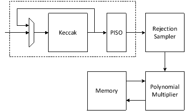
Keccak is used in SHAKE-128 configuration for rejection sampling operation. Hence, it will take the input data and generates 1344-bit output after each round. We propose implementing of Keccak while each round takes 12 cycles. The format of input data is as follows:
Input data = ρ | j | i
Where is seed with 256-bits, i and j are nonce that describes the row and column number of corresponding polynomial A such that:
Ai,j=Rejection_sampling(Keccak(ρ | j | i))
Since each 12-bit is used for one coefficient, each round of Keccak output provides 1344/12=112 coefficients. There are two paths for Keccak input. While the input can be set by controller for each new polynomial, the loop path is used to rerun Keccak for completing the previous polynomial. Rejection sampler cannot take all 1344-bit output parallelly since it makes hardware architecture too costly and complex, and also there is no other input from Keccak for the next 12 cycles. Therefore, we propose a parallel-input serial-output (PISO) unit in between to store the Keccak output and feed rejection unit sequentially.
The rejection sampler takes data from the output of SHAKE-128 stored in a PISO buffer. The required cycles for this unit are variable due to the non-deterministic pattern of rejection sampling. In our optimized architecture, this unit works in parallel with the Keccak core. Therefore, the latency for rejection sampling is absorbed within the latency for a concurrently running Keccak core.
Our proposed polynomial multiplier can perform point-wise multiplication on four coefficients per cycle that also helps to avoid memory access challenges and make the control logic too complicated. This implies that the optimal speed of the rejection sampling module is to sample four coefficients without rejection in one cycle.
On the output side, as the rejection sampling might fail, the rejection rate for each input is:
rejection_rate= 1-q212=1-3329212=0.187
Hence, the probability of failure to provide 4 appropriate coefficients from 4 inputs would be:
1-1-rejectionrate4=1-1-0.1874=0.56
To reduce the failure probability and avoid any wait cycle in polynomial multiplication, we need more coefficients are fed into rejection while only 4 of them will be passed to polynomial multiplication. This decision reduces the probability of failure. The following equation computes failure probability of having at least 4 valid samples out of N inputs:
PX≥4=1-k=03PX=k
PX=k=N k pk1-pN-k
The failure probability for different N as shown below:
| Number of Inputs (N) | Failure Probability |
|---|---|
| 4 | 0.56 |
| 5 | 0.23 |
| 6 | 0.08 |
| 7 | 0.02 |
| 8 | 0.007 |
| 9 | 0.002 |
| 10 | 0.0005 |
To balance the hardware resource utilization while improving the performance, we chose to have 10 input samples. Adding a FIFO to rejection sampling unit can store the remaining unused coefficients and increase the probability of having 4 appropriate coefficients to match polynomial multiplication throughput. The architecture is as follows:
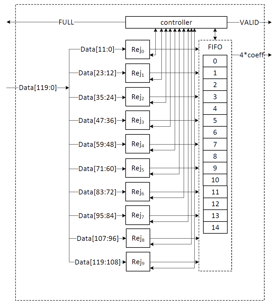
There are 10 rejection sampler circuits corresponding to each 12-bit input. The controller checks if each of these coefficients should be rejected or not. The valid input coefficients can be stored into the FIFO. While a maximum of 10 coefficients can be fed into FIFO, there are three more entries for the remaining coefficients from the previous cycle. There are several scenarios for the proposed balanced throughput architecture:
- At the very first cycle, or whenever the FIFO is empty, rejection sampling unit may not provide all 4 coefficients for the polynomial multiplication unit. We reduce the failure probability of this scenario by feeding 10 coefficients, however, it may happen. So, for designing efficient architecture, instead of reducing the failure probability by adding more hardware cost, we use a VALID output that stops the polynomial multiplier until all 4 required coefficients are sampled.
- If all 10 inputs are valid, they are going to be stored into FIFO. The first 4 coefficients will be sent to the polynomial multiplication unit, while the remaining coefficients will be shifted to the head of FIFO and be used for the next cycle.
- The FIFO has a maximum depth of 14 entries. When 9 or more entries are filled, a pop operation reduces the occupancy to 5, which is still insufficient to accommodate new inputs while allowing the rejection sampling unit to continue outputting data in upcoming cycles. As a result, the FIFO asserts the FULL flag to block further input from the Keccak core.
| Cycle count | Input from PISO | FIFO valid entries from previous cycle | Total valid samples | output | FIFO remaining for the next cycle |
|---|---|---|---|---|---|
| 0 | 10 | 0 | 10 | 4 | 6 (FULL) |
| 1 | 0 | 6 | 6 | 4 | 2 |
| 2 | 10 | 2 | 12 | 4 | 8 (FULL) |
| 3 | 0 | 8 | 8 | 4 | 4 |
| 4 | 10 | 4 | 14 | 4 | 10 (FULL) |
| 5 | 0 | 10 | 10 | 4 | 6 |
| 6 | 10 | 6 | 13 | 4 | 9 (FULL) |
- If there is not FULL condition for reading from Keccak, all PISO data can be read in 11 cycles. This would match with Keccak throughput that generates 112 coefficients per 12 cycles.
- The maximum number of FULL conditions is when there are no rejected coefficients for all 112 inputs. In this case, after every cycle with 10 coefficients, there is one FULL condition. It takes 28 cycles to process all PISO contents. To maximize the utilization factor of our hardware resources, Keccak core will check the PISO status. If PISO contains 8 coefficients or more (the required inputs for rejection sampling unit), EMPTY flag will not be set, and Keccak will wait until the next cycle. Hence, the Keccak output will be stored into PISO when all PISO contents are processed by rejection sampler.
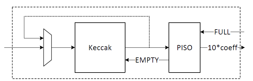
CBD sampler
ML-KEM ML-KEM, a lattice-based key encapsulation mechanism (KEM), relies on binomial sampling to generate small polynomials with coefficients following a centered binomial distribution (CBD). This distribution is crucial for ensuring cryptographic security while maintaining efficiency in polynomial arithmetic. In ML-KEM, the binomial parameter η varies depending on the security level, where η = 3 for ML-KEM-512 and η = 2 for ML-KEM-768 and ML-KEM-1024.
ML-KEM ML-KEM relies on a specialized distribution, D(Rq), to generate polynomials with small coefficients, commonly referred to as "errors" or "noise". This distribution is parameterized by an integer η. To generate a polynomial from D(Rq), each coefficient is sampled independently from a centered binomial distribution (CBD) over . The sampling process follows the following equation, which produces polynomial coefficient arrays based on an input stream of uniformly random bytes. Let be the Keccak output, the coefficients are computed as follows:
ei=j=0j=η-12iη+j-j=0j=η-12iη+η+j
which turns uniformly distributed samples into binomial distribution.
To have a configurable Hamming weight computation, the CBD sampler extracts 8η random bits per coefficient from a pseudorandom bit stream. Then it computes the Hamming weight difference between the first and second halves of these bits to derive the binomially distributed coefficient. A control unit dynamically adjusts the sampling logic based on the selected η value, allowing seamless reconfiguration.
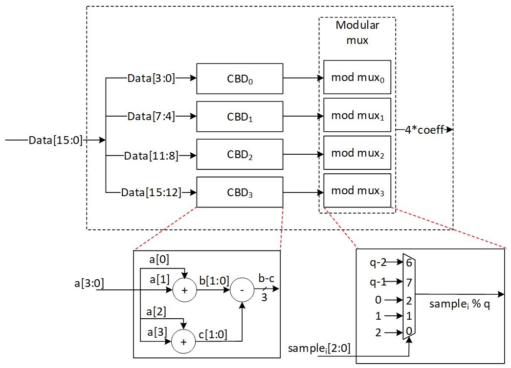
Our proposed data flow ensures that 4 coefficients are computed per cycle, significantly improving throughput compared to conventional serial samplers. A parallel-input serial-output (PISO) buffer is employed to manage input bitstreams efficiently, ensuring a steady supply of random bits.
The binomial sampler operates concurrently with Keccak, reducing overall latency. By leveraging a pipelined structure, the design ensures that binomial sampling does not become a performance bottleneck for polynomial arithmetic operations. A PISO buffer stores intermediate values, reducing redundant computations and improving resource utilization. The architecture supports dynamic switching between η values based on control signals, making it adaptable for different security levels.
For η = 2, each polynomial requires 1024 bits. Since SHAKE256 provides 1088 bits per round, a single Keccak round suffices. However, for η = 3, each polynomial requires 1536 bits (256 × 3 × 2 = 1536), necessitating two Keccak rounds to generate enough entropy.
The configurable design reduces hardware redundancy by allowing a single sampling unit to support multiple security levels. Generating 4 coefficients per cycle improves overall efficiency, aligning the sampler’s throughput with memory architecture, polynomial multiplication and other arithmetic operations. Parallelism and buffering mechanisms prevent stalls, ensuring that sampling latency does not impact system performance.
Compress/Decompress
The compression stage in ML-KEM takes full 12-bit polynomial coefficients and reduces them to a smaller representation of d bits, where d varies depending on the compression level. This design explicitly supports d values of 1, 5, 11, and 12. The value d = 12 is used to implement the byte encode and byte decode functions of the ML-KEM algorithm. This compression is a lossy operation that approximates a division by q = 3329, mapping each coefficient in Zq to a smaller domain suitable for compact ciphertext encoding. In hardware, this typically requires multiplication by a scaling factor, followed by division and rounding operations that are expensive in terms of logic and latency.

To optimize this process, we propose a hardware-efficient compression architecture that processes four 12-bit coefficients per clock cycle. Each coefficient undergoes configurable shifts and additions to approximate the division operation.
To accurately implement the compression formula in hardware, we adopt the following formula:
((data[11:0] << d) + q/2) / q
where data is a 12-bit coefficient and d is the target compressed bit-width. The term q2 is added prior to division to address the rounding behavior of hardware right shifts. In hardware implementations, division is implemented using right shifts, which inherently perform truncation (i.e., rounding down). This creates a systematic bias in the compressed output. By adding q2 before the division, we effectively round the result to the nearest integer rather than always rounding down. This adjustment is critical for maintaining the fidelity of the compression process and ensures that the mapping from Zq to the reduced d-bit representation is as accurate as possible, without introducing additional complexity to the hardware. The approach is both efficient and hardware-friendly, requiring only a simple addition and no costly division circuitry.
The following figure shows the compression map where d=1:

Rather than implementing a general-purpose division unit, which would significantly increase area, we leverage a dual-purpose Barrett reduction module, originally included for use in the Number-Theoretic Transform (NTT) and inverse NTT stages. This is a key novelty of our design: by reusing the Barrett logic for both modular reduction and compression scaling, we eliminate the need for redundant arithmetic units and improve overall resource utilization.
Barrett reduction is a well-established technique used in lattice-based cryptographic schemes to reduce coefficients modulo a fixed constant, such as q = 3329, in a way that avoids full-width division. With careful parameter selection, the Barrett algorithm can be optimized to require only a single level of conditional subtraction, making it highly suitable for high-speed and low-area hardware implementations.
In our architecture, the same logic is reused for the division required during compression, allowing efficient rounding without the overhead of full-precision arithmetic.
Following compression, decompression performs the inverse operation by expanding d-bit coefficients back to 12-bit values in Zq based on the following formula.
Our architecture handles four such compressed coefficients per clock cycle using four parallel multipliers. Each compressed coefficient is scaled and shifted based on its original encoding formula to recover the approximate 12-bit representation. The decompression path supports multiple d values via a configurable datapath, enabling seamless integration into systems supporting different compression profiles for ML-KEM using the following equation.
((data[d-1:0] * q) + (2^(d-1))) >> d
The addition of 2d-1 serves the same rounding purpose as q2 in the compression path. Since right shifts truncate in hardware, adding 2d-1 ensures the result is rounded to the nearest integer instead of being consistently biased downward. As with compression, the technique is hardware-friendly and avoids complex division or floating-point logic, while delivering improved accuracy through a simple constant addition and shift. The proposed architecture for decompression is shown as follows:
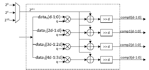
To maximize efficiency, the decompression and compression stages share arithmetic resources wherever possible. Multipliers, shift-add networks, and routing logic are multiplexed between the two operations, enabling compact hardware without sacrificing throughput. The shared Barrett reduction module is a central feature of this architecture, serving both traditional modular reduction in the NTT/INTT flow and the scaled division in compression.
This approach not only improves area efficiency but also simplifies integration and control logic. By avoiding dedicated division circuits and leveraging existing reduction infrastructure, our architecture delivers high-performance, low-area compression and decompression tailored for the demands of post-quantum cryptography.
High-Level architecture
In our proposed architecture, we define specific instructions for various submodules, including SHAKE256, SHAKE128, SHA3-512, SHA3-256, NTT, INTT, etc. Each instruction is associated with an opcode and operands. By customizing these instructions, we can tailor the engine's behavior to different security levels.
To execute the required instructions, a high-level controller acts as a sequencer, orchestrating a precise sequence of operations. Within the architecture, several memory blocks are accessible to submodules. However, it's the sequencer's responsibility to provide the necessary memory addresses for each operation. Additionally, the sequencer handles instruction fetching, decoding, operand retrieval, and overall data flow management.
The high-level architecture of Adams Bridge controller is illustrated as follows:
Sequencer
High-Level controller works as a sequencer to perform a specific sequence of operations. There are several blocks of memory in the architecture that can be accessed by sub-modules. However, the sequencer would be responsible for passing the required addresses for each operation.
As an example, an NTT operation needs to take three base addresses as follows:
NTT(initialvalue_base_address, intermediatevalue_base_address, result_base_address)
So, for performing a=NTT(b), the sequencer needs to be:
NTT(a_base_address, temp_base_address, b_base_address)
The following table lists different operations used in the high-level controller.
Keccak and samplers Opcodes:
| Instruction | Description |
|---|---|
| RST_Keccak | Reset the Keccak SIPO buffer |
| EN_Keccak | Enable the Keccak |
| LDKeccak_MEM src, len | Load Keccak SIPO buffer at memory address src in len -width |
| LDKeccak_REG src, len | Load Keccak SIPO buffer at register ID src in len -width |
| RDKeccak_MEM dest, len | Read Keccak PISO buffer and store it at memory address dest in len -width |
| RDKeccak_REG dest, len | Read Keccak PISO buffer and store it at register ID dest in len -width |
| REJ_SMPL | Start Keccak and rejection sampler (results is used by PWM) |
| CBD_SMPL | Start Keccak and CBD sampler |
NTT/INTT/PWO Opcodes:
| Instruction | Description |
|---|---|
| NTT src, temp, dest | Perform NTT on data at memory address src and store the results at address dest |
| INTT src, temp, dest | Perform INTT on data at memory address src and store the results at address dest |
| PWM src0, src1, dest | Perform PWM on data at memory address src0 and src1 and store the results at address dest (dest = src0*src1) |
| PWM_SMPL src, dest | Perform PWM on data from sampler and at memory address src and store the results at address dest (dest = smpl*src) |
| PWM_ACCU src0, src1, dest | Perform PWM in accumulation mode on data at memory address src0 and src1 and store the results at address dest (dest = src0*src1+dest) |
| PWM_ACCU_SMPL src, dest | Perform PWM in accumulation mode on data from sampler and at memory address src and store the results at address dest (dest = smpl*src + dest) |
| PWA src0, src1, dest | Perform PWA on data at memory address src0 and src1 and store the results at address dest (dest = src0+src1) |
| PWS src0, src1, dest | Perform PWS on data at memory src0 and src1 and store the results at address dest (dest = src0-src1) |
Other Opcodes:
| Instruction | Description |
|---|---|
| COMPRESS src, mode, dest | Perform compress on data at memory address src with mode configuration and store the results at address dest |
| DECOMPRESS src, mode, dest | Perform decompress on data at memory address src with mode configuration and store the results at address dest |
ML-KEM Memory Layout (Unmasked, MASKING_EN=0)
When
MASKING_EN = 1, eachinst0/inst1/inst2instance below has a same-dimension mirror with the_maskedsuffix holdingshare1; the regular instances holdshare0. The offset tables apply to both. Seeabr_mem_top.svfor the gated instantiation.
ML-KEM shares the same three memory instances as MLDSA. ML-KEM coefficients use MLKEM_COEFF_DEPTH = 64 entries per polynomial (256 coefficients / 4 per clock).
inst0 (ML-KEM)
| Offset | Entries | Name | Notes |
|---|---|---|---|
| 0- 255 | 256 | S0..S3 | CBD output / skDecode, 4x64 |
| 256- 447 | 192 | T0..T3 | A*s+e result (KeyGen) / pkDecode (Encaps), 4x64 |
| 512- 767 | 256 | E0..E3 | CBD noise, 4x64 |
| 768- 831 | 64 | MU | Decompress(msg) for Encaps |
| 832-1087 | 256 | U0..U3 | Encaps output / Decaps input, 4x64 |
| 1088-1151 | 64 | V | t*y+e2+mu result |
inst1 (ML-KEM)
| Offset | Entries | Name | Notes |
|---|---|---|---|
| 0- 63 | 64 | AS0 / AY0 / TY_MASKED / SU_MASKED | Accumulator scratch, reused per row |
inst2 (ML-KEM)
| Offset | Entries | Name | Notes |
|---|---|---|---|
| 0- 255 | 256 | Y0..Y3 / UP0..UP3 / TY / SU | Encaps r-vectors / Decaps NTT(u), 4x64 |
| 256- 319 | 64 | E_2 | CBD noise for Encaps |
KeyGen Data Flow
1. CBD -> S0..S3, E0..E3                               (inst0)
2. NTT(S_i), NTT(E_i) in-place                        (inst0)
3. For each row i=0..3:
   a. ExpandA x S_NTT -> AS0                           (inst0 read, inst1 write)
   b. AS0 + E_i -> T_i                                 (inst1 read + inst0 read -> inst0 write)
4. Compress(T) -> ek, Compress(S) -> dk                (inst0 read)
Decaps Data Flow
1. Decompress(dk) -> S0..S3                            (inst0)
2. Decompress(c1) -> U0..U3                            (inst0)
3. Decompress(c2) -> V                                 (inst0)
4. NTT(U_i) -> UP_i                                   (inst0 -> inst2)
5. S_i * UP_i -> SU_MASKED (accumulate)                (inst0 x inst2 -> inst1)
6. INTT(SU_MASKED) -> SU                               (inst1 -> inst2)
7. SU - V -> V                                         (inst2 - inst0 -> inst0 in-place)
8. Compress(V) -> msg                                  (inst0 read)
Encaps Data Flow
1. Decompress(ek) -> T0..T3                            (inst0)
2. CBD -> Y0..Y3 (inst2), E0..E3 (inst0), E_2 (inst2)
3. NTT(Y_i) in-place                                  (inst2)
4. For each row i=0..3:
   a. ExpandA x Y_NTT -> AY0                           (inst2 read -> inst1 write)
   b. INTT(AY0) -> AY0                                 (inst1 in-place)
   c. AY0 + E_i -> U_i                                 (inst1 + inst0 -> inst0)
5. T_i * Y_i -> TY_MASKED (accumulate)                (inst0 x inst2 -> inst1)
6. INTT(TY_MASKED) -> V                                (inst1 -> inst0)
7. Decompress(msg) -> MU                               (inst0)
8. MU + E_2 -> E_2                                     (inst0 + inst2 -> inst2)
9. V + E_2 -> V                                        (inst0 + inst2 -> inst0)
10. Compress(U) -> c1, Compress(V) -> c2               (inst0 read)
References:
[1] NIST, "FIPS 203 Module-Lattice-Based Key-Encapsulation Mechanism Standard," August 13, 2024.
Core Registers
Redirecting to external documentation...
Click here if not redirected ↗
84daa9a
Caliptra Subsystem Hardware Specification
Version 2p1
- Scope
- Caliptra Subsystem Requirements
- Caliptra Subsystem Architectural Flows
- I3C Streaming Boot (Recovery) Interface
- AXI Streaming Boot (Recovery) Interface
- Caliptra Core AXI Manager & DMA assist
- Caliptra Subsystem Fuse Controller
- Caliptra Subsystem Life Cycle Controller
- Caliptra Subsystem, SOC Debug Architecture Interaction
- Caliptra Subsystem LCC State Definitions
- DFT & DFD Life-cycle States
- LCC State and State Decoder Output Ports
- TAP Pin Muxing
- Production Debug Unlock Architecture
- Masking Logic for Debugging Features in Production Debug Mode (MCI)
- LCC Interpretation for Caliptra “Core” Security States
- Exception: Non-Volatile Debugging Infrastructure and Initial RAW State Operations
- LCC RAW Unlock Token Generation & Setting
- SOC LCC Interface usage & requirements
- LCC Module: Summarized Theory of operation
- Manufacturer Control Unit (MCU)
- Manufacturer Control Interface (MCI)
- Overview
- MCI Feature Descriptions
- MCI Debug
- MCI Design for Test (DFT)
Scope
This document defines technical specifications for a subsystem design utilizing Caliptra RoT in Subystem Mode. This document, along with Caliptra Hardware Specification, shall comprise the Caliptra Subsystem technical specification.
Document Version
| Date | Document Version | Description |
|---|---|---|
| Jan 31st, 2025 | v0p8 | Work in progress |
| Apr 30th, 2025 | v1p0-rc1 | Initial release candidate of Caliptra Gen 2.0 Subsystem Documents. Specifcations updated with: - Updated details on component features (MCU mailbox, MCU trace buffer, MCI error aggregation, FC fuse zeroization) - Details on design connectivity with top-level ports - Port and register updates |
| Oct 12th, 2025 | v2p1 | Final release of Caliptra Subsystem 2.1 |
Caliptra Subsystem Requirements
Definitions
- RA: Recovery Agent / Streaming boot Agent
- MCI: Manufacturer Control Interface
- MCU: Manufacturer Control Unit
Caliptra-Passive-Mode (Legacy)
SOC manages boot media peripherals and Caliptra is used as Root of trust for measurements.
Caliptra-subsystem-mode
Caliptra owns the recovery interface (peripheral independent) and Caliptra is THE RoT of the SoC. Any SOC specific variables that needs to be stored and retrieved securely from NV storage is handled using Caliptra.
Caliptra Subsystem Architectural Requirements
- MCU [Manufacturer Control Unit] runs Manufacturer specific FW authenticated, measured & loaded by Caliptra at boot time.
- MCU will use Caliptra RT FW to auth/measure/load all of the FW belonging to the SOC.
- MCU ROM/FW on MCU should be capable of performing SOC specific initialization.
- MCU ROM/FW should be able to perform SoC management functions including performing reset control, SoC specific security policy enforcement, SOC initial configuration (eg. any GPIO programming, glitch detection circuits, reading/moving non-secret fuses etc.).
- Note: Widgets that toggle the reset or other wires that set security permissions are SOC specific implementations.
- Fuse controller for provisioning Caliptra fuses -> IFP (In-field programmable) fusing is performed by MCU RT; SW partition fuses in fuse controller are managed by MCU (ROM or RT); Caliptra HW is responsible for reading the secret fuses (Caliptra ROM, MCU ROM or any other SOC ROM or any RT FW should NOT have access to read the secret fuses in production).
- Recovery stack must be implemented. Please refer to I3C recovery section for more details and references. OCP Recovery registers implemented in I3C must follow the security filtering requirements specified in the recovery implementation spec (eg. MCU can ONLY access subset of the recovery registers as defined by the recovery implementation).
- Supports silicon t0 boot to load and run required FW across chiplets.
- OCP recovery stack is implemented in Caliptra for Caliptra-subsystem-mode
- MCU SRAM (or part of the SRAM that is mapped for Code/Data execution) should be readable/writeable ONLY by Caliptra until Caliptra gives permission to MCU to use it.
- Caliptra can only load its FW, SOC manifest and MCU FW by reading the recovery interface registers.
- Caliptra ROM should know the offset of the recovery interface at its boot time. SOC has a choice to program this interface using MCU ROM or Hard strapped register address at integration time (Hard strapping at SOC integration time is recommended)
- Caliptra HW must know the offset of the registers where secrets (UDS, FE) and assets (PK hashes) exist at boot time. These should be hard strapped/configured at integration time.
- Caliptra ROM must know the address to where UDS-seed needs to be written to; this address should be hard strapped/configured at integration time.
- Any registers holding secrets/assets in fuse controller must follow the same rules as Caliptra 1.0/2.0 fuse register requirements (eg. clear on debug, clear on read once etc.)
- MCU SRAM and ROM sizes should be configurable at SOC integration time.
Caliptra Subsystem HW Requirements
Caliptra 2.0 HW requirements (Subsystem Support)
- Full AXI read/write channels (aka AXI manager) for subsystem (for MCU and Caliptra) a. For backward compatibility, AXI mgr. interface can be a no-connect and that configuration is validated.
- HW logic/Programmable DMA
- Read MMIO space for variable length.
- Data returned from the above read can be exposed directly to the FW OR allow it to be written to a subsystem/SOC destination as programmed by ROM/FW.
- Programmable logic to allow for SOC directed writes (from FW or from the above route back) to be sent through the SHA accelerator.
- (Future open/stretch goal): If AES engine accelerator is integrated into Caliptra, then implement decryption before sending the writes back to the destination programmed by the ROM/FW.
- This widget should have accessibility in manufacturing and debug mode over JTAG (can be exposed using the same JTAG interface as Caliptra 1.0). Ensure through validation that no asset can be read using this widget in those modes.
- Expand manuf flow register to include UDS programming request steps
- SOC Key Release HW (Required for OCP Lock flow too)
- Separate SOC Key Vault must be implemented (it is a separate structure from the current Caliptra KV).
- In at least one configuration, the SOC KV must be implemented as an SRAM that is external and configurable by the SOC OR or an internal configurable SOC KV structure. If this is achievable within the Caliptra 2.0 milestone, only one of these would be the chosen implementation and configuration. This will be a design decision based on effort & schedule.
- If implemented as a SRAM, data written and read into the SOC KV SRAM is decrypted & encrypted so that SOC DFT or other side channels cannot exfilterate the data.
- Caliptra FW will indicate to the SOC KV Release HW to release the key by supplying the key handle to read from.
- Destination address to which the key must be written to is programmed by the Caliptra FW into AXI MGR DMA HW.
- SOC KV must have the same attributes as Caliptra internal KV. Additionally, it must also have an attribute of read-once and clear.
Caliptra 2.0 HW requirements (Not subsystem related)
- Ability to use two or more cryptos concurrently
- Change APB -> AXI-Sub with the same capabilities (AXI USERID filtering replaces PAUSER based filtering, multiple targets for SHA acc, mailbox, fuses, registers etc. all)
- Future/Stretch Goal: Parity support on AXI-SUB & MGR
MCU HW requirements
- MCU should not be in the FIPS boundary and must not have any crypto functions. MCU must use Caliptra for any security flows (eg. security policy authorization) or traditional RoT support (eg. SPDM).
- MCU VeeR must support PMP & User mode.
- MCU AXI is directly connected to the SOC fabric in a way that allows a MMIO based control of the SoC as required for SOC security, manageability and boot functionality.
- MCU HW should add AXI-ID without any involvement of the ROM or FW running on the MCU; Implying any AXI access out of MCU (LSU side) should carry MCU USERID that HW populates.
- MCU executes from a SRAM that is at subsystem level.
- MCU uses instruction cache for speed up
- It is required that all NV read/writes (eg. NV variables in flash) that require a RoT support to securely store/restore must go through Caliptra.
- NV-storage peripheral shall be built in such a way that it will only accept transactions from MCU.
- Support for MCU first fetch vector to direct towards MCU SRAM post reset
Subsystem Components HW requirements
Fabric
- AXI Interconnect connects Caliptra, I3C, Fuse Controller, Life Cycle Controller, MCU and its memory components with the rest of the SOC.
- Note: Because each SOC integration model is different, AXI interconnect is NOT implemented by the subsystem but subsystem must validate using an AXI interconnect VIP to ensure all the components operate per the flows documented in this specification.
- For the VIP interconnect configuration, all subtractively decoded transactions are sent towards SoC. AXI interconnect & Subsystem is validated with the assumption that all of them are running on the same clock domain.
- To be documented: AXI-USERID requirements
MCU SRAM
- Since it's used for instruction and data execution – therefore requires AXI Sub with USERID filtering.
- Provide JTAG accessibility to allow for SRAM to be populated in a secured debug mode at power on time (debug policies will be same as Caliptra)
- MCU SRAM should have an aperture that can only be unlocked by Caliptra after it loads the image
- MCU SRAM has an aperture for MCU ROM to use part of the SRAM as a stack for its execution.
- MCU SRAM supports an aperture to be used as a MCU Mailbox.
MCU ROM
- MCU ROM also needs to have AXI Sub for any data access from MCU and thereby requires AXI-ID/USERID filtering.
I3C
- I3C on AXI interconnect with AXI Subordinate
- Spec 1.1.1 aligned, but only with optional features that are required per PCIe ECN # <>
- AXI Sub must be supported.
- UserID to MCU and Caliptra
- MCU access lock for I3C recovery and data (FIFO) registers until recovery flow is completed. In other words, MCU ROM must not impact the data flow into Recovery IFC registers. Stretch Goal: DMA data payload back to destination (Caliptra or MCU)
Fuse Controller
- AXI sub interface
- Secrets (separate USERID and access constraints) vs SW partition separation
- Registers implemented for “Secrets” should follow the same rules as Caliptra (no scan, clear on specific life cycle/security states)
- Life cycle transition shall be implemented in hardware with no ROM/FW implementation and provides redundancy against fault & glitch attacks in the digital logic itself.
- SOC debug in production mode shall be supported with the help Caliptra through post quantum resilient algorithms.
- When debug mode is intended to be enabled & when enabled, all secrets/assets as defined should be wiped and provide the indication to SOC for any secrets/assets it may have.
MCI
- HW logic to move secret fuses from Fuse controller to Caliptra.
Caliptra Subsystem Hardware Block Diagram
Figure: Caliptra Subsystem Block Diagram

Caliptra Subsystem Architectural Flows
Please refer to Caliptra Security Subsystem Specification for more details.
I3C Streaming Boot (Recovery) Interface
The I3C recovery interface acts as a standalone I3C target device for recovery. It will have a unique address compared to any other I3C endpoint for the device. It will comply with I3C Basic v1.1.1 specification. It will support I3C read and write transfer operations. It must support Max read and write data transfer of 1-256B excluding the command code (1 Byte), length (2 Byte), and PEC (1 Byte), total 4 Byte I3C header. Therefore, max recovery data per transfer will be limited to 256-byte data.
I3C recovery interface is responsible for the following list of actions:
- Responding to command sent by Recovery Agent (RA)
- Updating status registers based on interaction of AC-RoT and other devices
- Asserting / Deasserting “payload_available” & “image_activated” signals
Streaming Boot (Recovery) Interface hard coded logic
Hardware registers size is fixed to multiple of 4 bytes, so that firmware can read or write with word boundary. Address offset will be programmed outside of the I3C device. Register access size must be restricted to individual register space and burst access with higher size must not be allowed.
Figure: I3C Streaming Boot (Recovery) Interface Logic Block Diagram
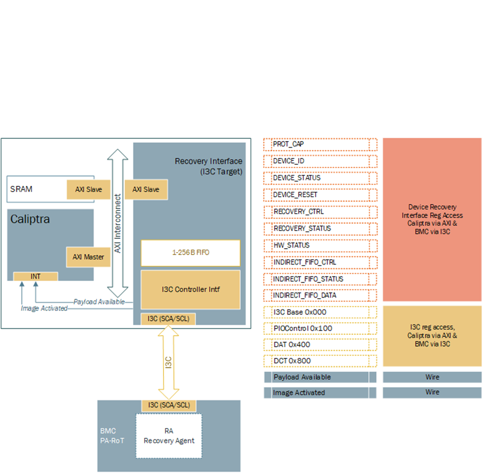
Hardware Registers
Hardware registers size is fixed to multiple of 4 bytes, so that firmware can read or write with word boundary. Address offset will be programmed outside of the I3C device. Register access size must be restricted to individual register space and burst access with higher size must not be allowed.
Note: Accessing the same address for INDIRECT_FIFO_DATA register will write or read the FIFO. It will not be available to access randomly as specified by the specification.
TODO: Add a link to rdl -> html file
Streaming Boot (Recovery) Interface Wires
- Payload available
- The Recovery Interface (I3C target) should receive a write transaction to INDIRECT_FIFO_DATA reg from BMC - 256B + 4B (Header), and wait for each I3C write to finish. Once I3C write transaction to INDIRECT_FIFO_DATA register is completed and PEC verification is successful, then the I3C target must assert "payload_available". DMA assist must wait for "payload_available" before reading. It must read 256B or last read with remaining data.
- The "payload_available" signal remains asserted until Recovery Interface receives Read from DMA over AXI for INDIRECT_FIFO_DATA.
- Image_activated
- The I3C target will assert "image_activated" signal as soon as write to RECOVERY_CTRL register is received.
- ROM will clear “image_activated” bit by writing to RECOVERY_CTRL register via DMA assist after the image is authenticated. As defined in the OCP Recovery Specification, RECOVERY_CTRL, byte 2 is used to specify the image activation control, and is Write-1-Clear. ROM must write 0xFF to this field to clear the image recovery status, which will also result in the Recovery Interface deasserting the “image_activated” signal to Caliptra.
I3C Streaming Boot (Recovery) Flow
Please refer to Caliptra Subsystem OCP Streaming Boot Sequence.
Figure: Caliptra Subsystem I3C Streaming Boot (Recovery) Flow
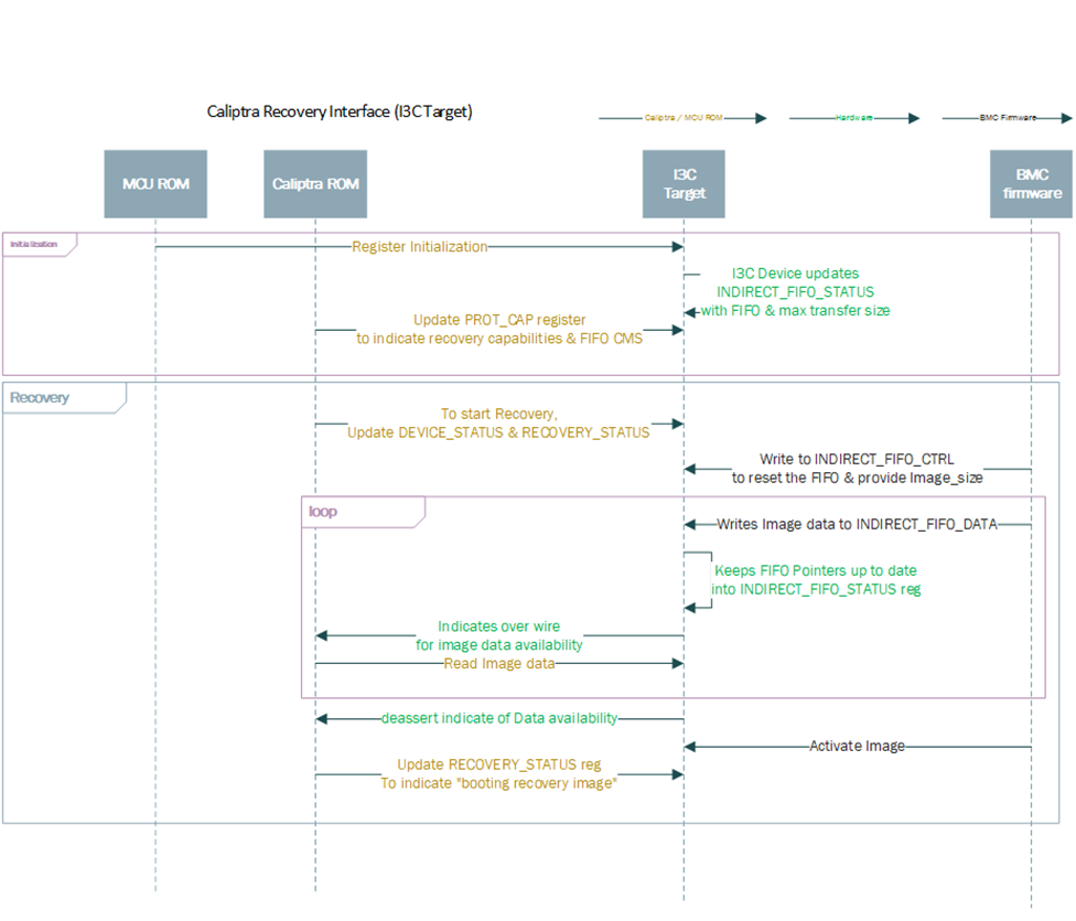
Caliptra ROM Requirements for OCP Streaming Boot
Caliptra firmware must follow these rules when implementing the OCP Streaming Boot flow:
- Caliptra ROM and RT Firmware must wait for "image_activated" signal to assert before processing the image.
- When image is sent to Caliptra Subsystem, Caliptra ROM & RT firmware must program DMA assist according to the rules defined in OCP Streaming Boot Payloads.
- Once the image is processed, Caliptra ROM & RT firmware must initiate a write with data 1 via DMA to clear byte 2 “Image_activated” of the RECOVERY_CTRL register. This will allow BMC (or streaming boot initiator) to initiate subsequent image writes.
I3C and Caliptra-AXI Interactions
Received transfer data can be obtained by the driver via a read from XFER_DATA_PORT register. Received data threshold is indicated to BMC by the controller with TX_THLD_STAT interrupt if RX_THLD_STAT_EN is set. The RX threshold can be set via RX_BUF_THLD. In case of a read when no RX data is available, the controller shall raise an error on the frontend bus interface (AHB / AXI).
AXI Streaming Boot (Recovery) Interface
This feature allows streaming data or firmware by MCU over the AXI bus of the I3C module which is repurposed as a streaming boot interface while disabling I3C usage.
AXI Streaming Boot Flow implementation
The AXI Streaming Boot flow reuses the logic already present in the I3C core used in the Caliptra-SS design, with a runtime option essentially bypassing most of the I3C core communication logic (including the I3C recovery flow logic).
The loopback functionality is configurable via the REC_INTF_CFG CSR which is set to I3C mode by default.
Streaming boot CSRs are accessible over AXI.
The transactions to the I3C core may be filtered using the AXI ID field.
The logic is implemented so that the streaming boot implementation in the Caliptra core (HW & ROM) can operate without any changes.
In order to enable setting W1C streaming boot registers, AXI streaming mode introduces an additional register - REC_INTF_REG_W1C_ACCESS.
AXI Streaming Boot Handler
In the regular (I3C) mode of the core, the Streaming Boot (Recovery) Handler strongly relies on the communication with the I3C Core internal logic by interfacing with TTI Queues. The bypass implementation modifies the I3C Core logic to allow direct access over the AXI bus to the structures specified by the OCP Streaming boot for compliance with the Caliptra Subsystem Streaming Boot Sequence.
The default design of the Streaming Boot Handler includes many blocks specifically designed to translate I3C bus traffic into recovery messages. It also automatically responds to the I3C commands by writing transaction descriptors and data for the TTI Queues.
Figure: Streaming Boot (Recovery) Handler in the I3C Core
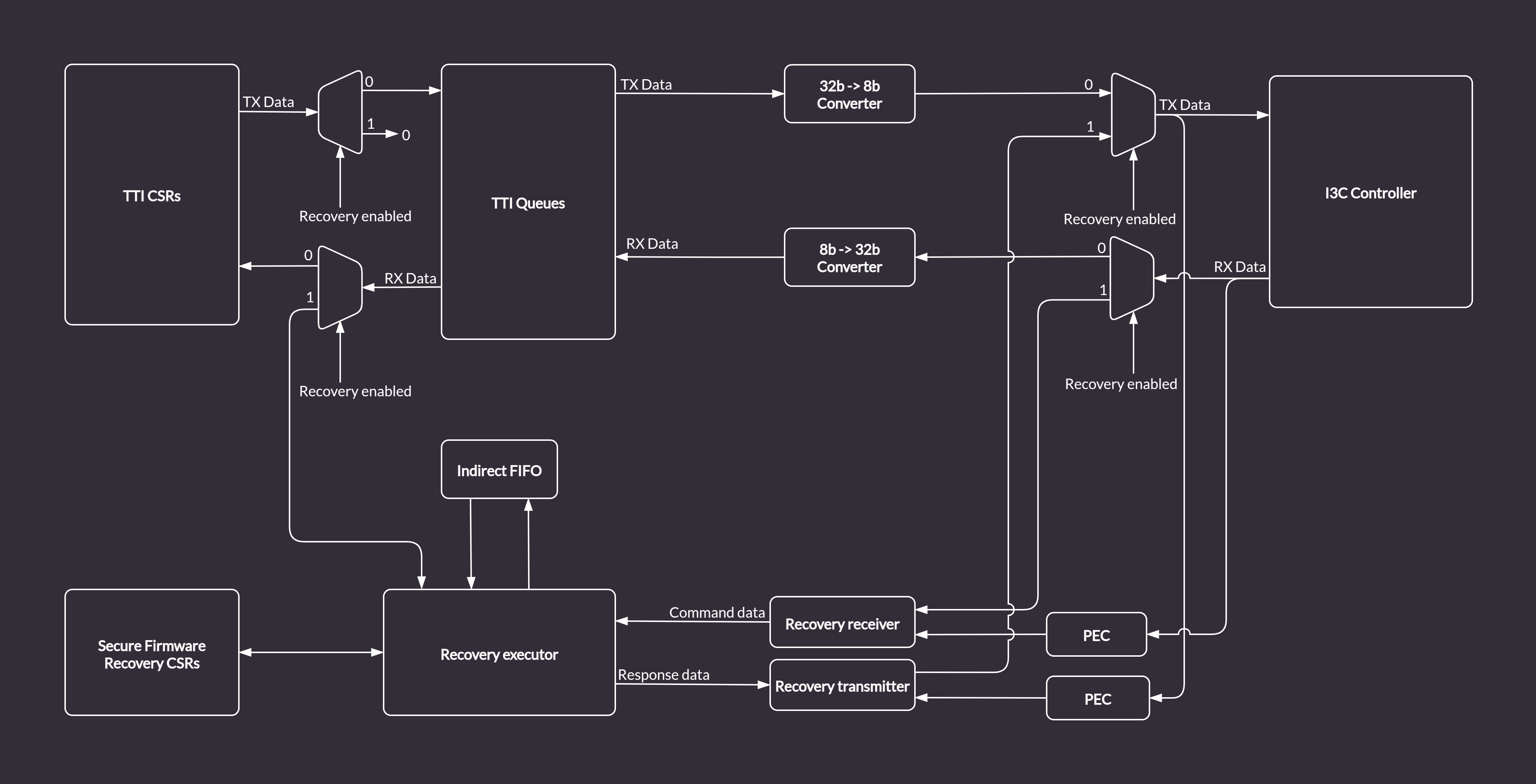
In order enable the AXI streaming boot mechanism while reusing the existing logic and keeping compliance with Caliptra, the I3C core provides a custom bypass feature allowing direct communication with the Streaming Boot Handler via the AXI bus. The bypass disables the I3C communication logic. Data is routed from the TTI TX Queue to the Recovery Executor block, and written directly to the Indirect Data FIFO. The Caliptra ROM can access the data from the Indirect FIFO over the AXI bus (the same way it does in the regular I3C streaming boot flow). The dataflow in bypass mode (marked with green arrows) is depicted in the diagram below.
Figure: AXI Streaming Boot Handler in I3C Bypass Mode

AXI Streaming Boot CSRs
With the bypass feature enabled, the FIFO status CSRs in the Streaming Boot CSR file will be updated by the Streaming Bott Handler module.
However, some registers like e.g. INDIRECT_FIFO_CTRL which are updated by I3C commands in a standard streaming boot flow, will have to be accessed and configured properly from the software running on the Caliptra MCU via the AXI bus.
All configurable registers are writable from software, read only registers provide status information about Streaming Boot Handler internals, e.g. details about size and fill level of the Indirect FIFO.
Caliptra Core AXI Manager & DMA assist
SOC_IFC includes a hardware-assist block that is capable of initiating DMA transfers to the attached SoC AXI interconnect. The DMA transfers include several modes of operation, including raw transfer between SoC (AXI) addresses, moving data into or out of the SOC_IFC mailbox, directly encrypting/decrypting images with the AES block, and directly driving data through AHB CSR accesses to datain/dataout registers. One additional operating mode allows the DMA engine to autonomously wait for data availability via the OCP Recovery interface (which will be slowly populated via an I3C or similar interface).
Caliptra arms transfers by populating a transaction descriptor to the AXI DMA CSR block via register writes over the internal AHB bus. Once armed, the DMA will autonomously issue AXI transactions to the SoC until the requested data movement is completed. The DMA uses an internal FIFO to buffer transfer data. For any transfer using AXI Writes (Write Route is not disabled), the DMA waits until sufficient data is available in the FIFO before initiating any AXI write requests.
When arming the engine, Caliptra firmware is expected to have information about available AXI addresses that are legal for DMA usage. The DMA can facilitate transfer requests with 64-bit addresses. DMA AXI Manager logic automatically breaks larger transfer sizes into multiple valid AXI burst transfers (max 4KiB size), and legally traverses 4KiB address boundaries. The DMA AXI Manager supports a maximum transfer size of 1MiB in total. FIXED AXI bursts are allowed, to facilitate a FIFO-like operation on either read or write channels.

AXI Feature Support
The DMA assist initiates transactions on the AXI manager interface in compliance with the AXI specification. The generated AXI transactions adhere to the following rules:
- All address requests will be aligned to the data width of the interface, which is configured as 32-bit in the 2.0 release.
- The DMA will not issue Narrow transfers. That is, AxSIZE will always be set to match the data width of the interface (4 bytes).
- All data lanes are used on all transfers. That is, the AXI manager Write channel will always set WSTRB to all 1s.
- At most, 2 reads and 2 writes will be initiated at any time.
- When using a non-zero block_size for the transfer, in accordance with the Streaming Boot feature, at most 1 read and 1 write will be issued concurrently.
- All transactions are initiated with AxID = 0, meaning that both reads and writes require in-order responses.
- The maximum burst length initiated is constrained by the following parameters:
- Any transfer using the INCR burst type is restricted by both the maximum allowable length of an AXI transaction (AxLEN=255 or total byte count of 4KiB, whichever is smaller) and the size of the internal FIFO. In the 2.0 release the internal FIFO is configured with a depth of 512 bytes; the maximum transaction size allowed is 256 bytes, to allow up to 2 transactions to be outstanding at a time. In summary, the transfer size will always be 256 bytes or less (AxLEN = 63), as this is the smallest of (AxLEN = 255 -> 1KiB, 4KiB, and 256 bytes).
- Any transfer using the FIXED burst type is restricted by the AXI specification to a burst length of 16.
- When the block_size field is set to a non-zero value when arming the DMA, all transfers are restricted in size to specified block_size, in bytes.
- AXI transactions must not cross a 4KiB boundary, per the specification. If the transfer size requires crossing a boundary, the DMA will break it into smaller transactions that will go up to the boundary, then start from the next alignment boundary.
Routes
In the AXI DMA control state machine, both the read and write interfaces have their own “route”. A route is configured for read and write channels for every DMA operation that is requested. Routes determine how data flows through the DMA block.
Read routes always apply when an AXI read is requested and must be disabled otherwise. Any AXI read pushes the response data into the internal FIFO. The read route determines where this data is ultimately sent when it is popped from the FIFO. For the AHB route, data from the FIFO is populated to the dataout register, where it may be read via AHB by the Caliptra RV core. For the mailbox route, data from the FIFO flows into the mailbox; for these operations, the mailbox address is determined by the destination address register value, with an offset applied based on how many bytes have been written to the mailbox. For the AXI route, data from the FIFO flows into the AXI Write Manager, whereupon it is sent out to AXI on the WDATA signal. For the Read DISABLE route, data output from the FIFO always flows into the AXI write channel. In this case, data originates from a source other than an AXI read, so AXI reads are inactive.
Write routes always apply when an AXI write is requested and must be disabled otherwise. Any AXI write reads data from the internal FIFO before sending it over AXI. The write route determines where this data originates before it is pushed onto the FIFO. For the AHB route, a write to the datain register via AHB results in write data being pushed onto the FIFO. For the mailbox route, data is read from the mailbox and pushed onto the FIFO; for these operations, the mailbox address is determined by the source address register value, with an offset applied based on how many bytes have been read from the mailbox. For the AXI route, data flows from the AXI Read Manager into the FIFO. For the Write DISABLE route, data received on the AXI read channel is always pushed into the FIFO and then sent to an internal destination rather than a destination on the AXI bus, so AXI writes are inactive.
Example 1: Write Route == MBOX and Read Route == DISABLE

Example 2: Read Route == AHB and Write Route == DISABLE
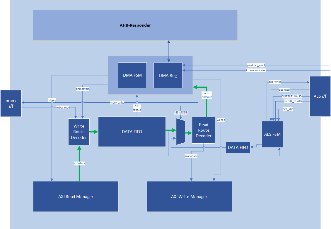
Example 3: Read Route == AXI and Write Route == AXI
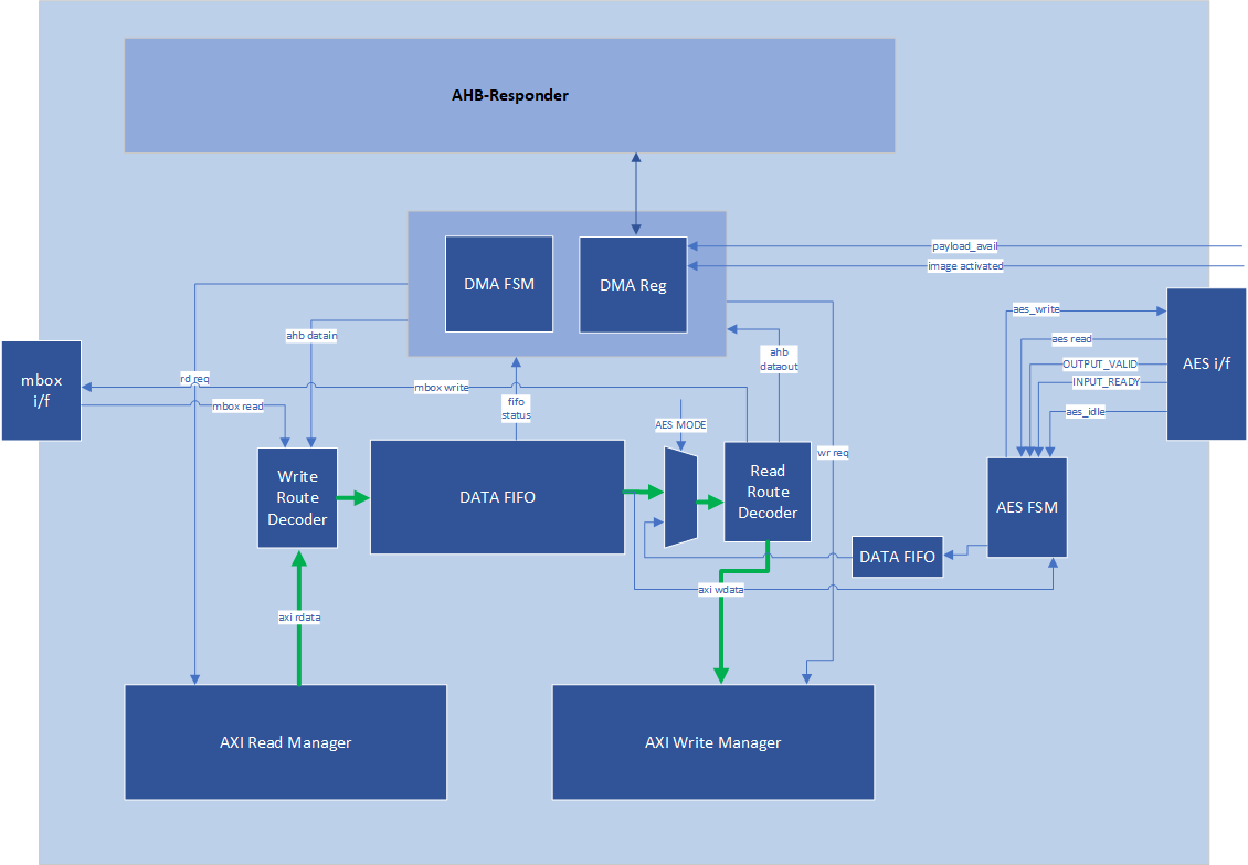
OCP Streaming Boot Payloads
The DMA block supports a special mode of operation that is intended for use in reading Firmware Image Payloads (for Streaming Boot) from the Recovery Interface, present in the Caliptra Subsystem. This operation mode relies on three key control signals: the payload_available signal input from the recovery interface, the read_fixed control bit, and the block_size register (from the DMA control CSR block).
This special mode of operation is only used for AXI Reads. To trigger the DMA to operate in this mode, Caliptra Firmware must program the block_size register to a non-zero value that is a power-of-two. Caliptra Firmware must also program the read_fixed control bit. Once the “go” bit is set, causing the DMA to begin operation, the DMA control logic will wait for the payload_available input to trigger. When this occurs, the DMA controller issues a read that has a size equal to (or smaller) than the configured block_size (the read may be smaller if required by AXI rules). This process repeats until the amount of data indicated in the byte_size register has been transferred.
When programming an AXI to AXI transfer for a Streaming Boot Payload (e.g., to transfer an SoC Firmware manifest into an AXI-attached SRAM), firmware must also follow these rules:
- Programmed value of block_size must not exceed the largest legal AXI transaction size for a FIXED burst type. The DMA assist has a native data width of 4-bytes, so transaction size is restricted to 64-bytes due to the AXI specification limit of AxLEN == 15 for FIXED transactions.
- Destination address must be aligned to the programmed value of block_size. For example, if block_size is set to 64-bytes, destination address must be an integer multiple of 0x40.
In all cases other than reading Recovery Interface Payloads, the block_size register must be programmed to 0.
AES Mode
The DMA block can directly stream images from AXI to AES for decrypt/encrypt, and then stream the processed image over AXI to some SOC storage. This can be done by configuring the AXI DMA as:
- AES Mode == 1
- (optional) aes_gcm_mode in DMA == 1
- Read Route == AXI
- Write Route == AXI
- Block Size == 0 (OCP Stream Boot Disabled)
- Read/Write Fixed == 0
- Source Address == Start of image
- Destination Address == Start address where processed image should be stored
- Configure Byte Count - must be DWORD aligned
Other Read/Write Routes and Block sizes are not supported.
The AXI DMA AES Mode ONLY streams the image into and out of AES. It is Firmware's responsibility to:
- Fully configure AES before streaming the image via AXI DMA
- Push the IV, AAD header, and any other data into AES before streaming the image via AXI DMA
- Retrieve any tags from AES after the image has been processed.
If the input image size is not a multiple of 4 DWORDS, the AES FSM will properly pad the AES input data with 0s. When streaming the image out it reads all 4 DWORDS from the AES, but only writes up to the last DWORD of the image to the destination. If aes_gcm_mode register is set, at the start of the transfer it updates the GCM shadow byte count and phase registers in AES to the appropriate byte count and GCM_TEXT phase. Before the last block transfer to the AES it will again update the GCM shadow register to the appropriate values.
Input images can be in little endian or big endian. It is FW's responsibility to configure the AES wrapper's ENDIAN_SWAP register.
If AXI DMA encounters any errors (AXI or other errors) it will finish the transfer and report an error. It is the Firmware's responsibility to clear the error in the AXI DMA and flush the AES if required.
When AXI DMA is using AES Caliptra shall not try to access AES via AHB until AXI DMA has completed.
AES is not directly exposed on the AXI bus for external entities, it is protected behind the AXI DMA and can only be accessed via Caliptra uC AHB or the Caliptra DMA.
AES Mode: Read Route == AXI, Write Route == AXI, AES Mode == 1
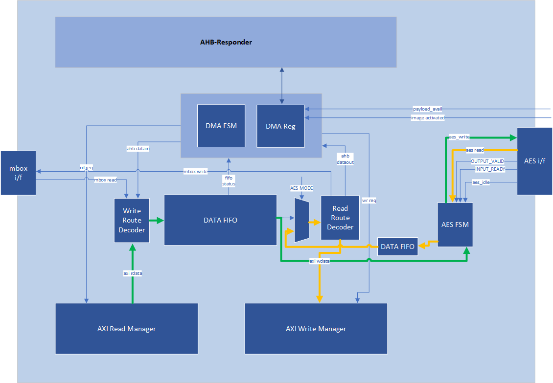
Programming Flowchart
General Rules:
- If either Read or Write route is configured to AXI RD -> AXI WR, both routes must be configured as AXI RD -> AXI WR.
- Read Route and Write Route must not both be disabled.
- If Read Route is enabled to any configuration other than AXI RD-> AXI WR, Write route must be disabled.
- If Read Route is disabled, Write route must be enabled to a configuration that is not AXI RD -> AXI WR.
- If Read Route is disabled, Read Fixed field is ignored.
- If Write Route is disabled, Write Fixed field is ignored.
- Addresses and Byte Counts must be aligned to AXI data width (1 DWORD).
- Block Size is used only for reads from the Subsystem Recovery Interface. When block size has a non-zero value, the DMA will only issue AXI read requests when the payload available input signal is set to 1, and will limit the size of read requests to the value of block size. For all other transactions (such as AXI writes, or any single-dword access to a subsystem register via the DMA), block size shall be set to a value of 0 for every transaction.
- AES mode is only valid with Read/Write routes AXI RD -> AXI WR, Read/Write Fixed = 0, and Block Size 0.
Steps:
- Write Byte Count
- Write Block Size
- Write Source Addr (value is ignored if data is from AHB)
- Write Dest Addr (value is ignored if data is to AHB).
- To perform an accelerated SHA operation on incoming read data, firmware sets the Read/Write route to AXI RD-> AXI WR, and the destination address to the SoC address for the SHA Acceleration data in aperture.
- Set Interrupt Enables (optional)
- If Mailbox R/W: Acquire Mailbox Lock
- If SHA Acc Op:
- First acquire Sha Accel Lock via AXI by using this flow (with the AHB-> AXI WR route) to initiate AXI manager action
- Initiate Sha Accel streaming operation via AXI by using this flow (with the AHB-> AXI WR route) to initiate AXI manager action
- Run this operation with the AXI RD -> AXI WR route to move data from SoC location into Sha Accelerator
- If AES Mode:
- Fully configure AES with IV/KEY see AES spec for more details
- Stream in any header info to AES like AAD
- Set read/write routes to AXI
- Set AES_MODE in DMA
- Set aes_gcm_mode in DMA if this is the AES mode
- Set Control Register
- Set Read/Write Routes
- Set Read/Write Fixed=0/1
- GO
- (All 3 may be single write or separate, GO must be last bit to set)
- If AHB data: Wait for RD FIFO not empty or WR FIFO not full
- Push/Pop data (using Rd Data/Wr Data register offsets) until all requested bytes transferred
- If AHB Error – check status0 for Error, then check for “Command Error”
- Wait for TXN Done Interrupt (or Poll Status0)
- Read Status0, confirm Busy=0, Error=0
Descriptor
https://chipsalliance.github.io/caliptra-rtl/main/internal-regs/?p=clp.axi_dma_reg
Caliptra Subsystem Fuse Controller
FUSE controller is an RTL module that is responsible for programming and reading the FUSEs. This module has an AXI interface that is connected to Caliptra Subsystem’s AXI interconnect. This module provides the device with one-time programming functionality, resulting in non-volatile programming that cannot be reversed. This functionality is delivered via an open-source FUSE Controller and a proprietary FUSE/OTP Macro. This RTL module manages the following FUSE partition mapping, which can be found in the Fuse Controller Memory Map.
Partition Details
The Fuse Controller is configured a total of 16 partitions (See Fuse Controller's Fuse Partition Map), while it can support different number of partitions based on SoC product requirements. Secret FUSE partitions are prefixed with the word "Secret" and are associated with specific Life Cycle (LC) states, such as "MANUF" or "PROD." This naming convention indicates the LC state required to provision each partition.
Key Characteristics of Secret Partitions
- Programming Access:
UDS_SEEDandFIELD_ENTROPYpartitions can only be programmed by the Caliptra Core.- Secret partitions are buffered, meaning they are stored in registers and are erased (temporarily zeroized) if Caliptra-SS enters debug mode.
- Locking Mechanism:
- Write access to a partition can be permanently locked when no further updates are required.
- To lock a partition, an integrity constant is calculated and programmed alongside the data for that partition.
Partition-Specific Behaviors
Life Cycle Partition
- The life cycle partition remains active across all stages and cannot be locked.
- This ensures that the device can transition back to the RMA state in case of unexpected failures during production.
Vendor Test Partition
- The vendor test partition is used for FUSE programming smoke checks during manufacturing.
- Unlike other partitions, ECC uncorrectable errors in this partition do not trigger fatal errors or alerts due to the nature of FUSE smoke checks, which may leave certain FUSE words in inconsistent states.
Locking the Validated Public Key Partition
During firmware authentication, the ROM validates the vendor public keys provided in the firmware payload. These keys, which support ECC, MLDSA, and LMS algorithms, are individually hashed and compared against stored fuse values (e.g., CPTRA_CORE_VENDOR_PK_HASH_n). Once a valid key is identified, the ROM locks that specific public key hash and all higher-order public key hash entries for the remainder of the current boot. This ensures that the validated key’s fuse entry remains immutable until the next subsystem reset (warm or cold) re-runs the boot flow. Importantly, the locking mechanism is applied only to the public key hashes. The associated revocation bits, which allow for runtime key revocation, remain unlocked. To support this, the fuse controller (FC) implements two distinct partitions:
-
PK Hash Partition
- Purpose:
- Contains the
CPTRA_CORE_VENDOR_PK_HASH[i]registers for i ranging from 1 to N. - Once a key is validated, the corresponding hash and all higher-order hashes are locked by MCU ROM via the volatile lock CSR, making them immutable for the rest of the current boot. The lock clears on any subsystem reset (warm or cold), at which point the FC re-runs OTP init and ROM re-validates.
- Contains the
- Layout & Details:
- Partition Items:
CPTRA_CORE_VENDOR_PK_HASH[i]where i ranges from 1 to N.- Default N: 1
- Maximum N: 16
- Size: N × 384 bits (each hash is 384-bit)
- Programming:
- The first key (i=1) is programmed during the manufacturing phase.
- The remaining keys (if any, i.e., N–1) can be programmed during manufacturing or in the field (production).
- Partition Item:
CPTRA_CORE_VENDOR_PK_HASH_VALIDis used to indicate which of the N keys is valid. Therefore, the length is N to support N-bit hot-encoding.
- Partition Items:
- Purpose:
-
PK Hash Revocation Partition
- Purpose: This partition stores runtime-updateable revocation bits and PQC type information.
- Layout & Details:
- For each vendor public key (
VENDOR_PK_HASH[i]), the partition contains:- ECC Revocation Bits: 4 bits (e.g.,
CPTRA_CORE_ECC_REVOCATION[i]) - LMS Revocation Bits: 32 bits (e.g.,
CPTRA_CORE_LMS_REVOCATION[i]) - MLDSA Revocation Bits: 4 bits (e.g.,
CPTRA_CORE_MLDSA_REVOCATION[i]) - PQC Key Type Bits: 1-bit one-hot encoded selection (e.g.,
CPTRA_CORE_PQC_KEY_TYPE[i])
- ECC Revocation Bits: 4 bits (e.g.,
- Attributes:
- This partition is kept separate from the PK hash partition to allow for runtime updates even after the validated public key is locked.
- For each vendor public key (
-
Volatile Locking Mechanism
-
The FC implements volatile write locks with sticky W1S CSRs. Each lock bit is effectively write-once per boot: writing a 1 sets the selected lock bit; writing 0 cannot clear an already-set bit. Once set, the bit remains set for the rest of the current boot and clears on the next subsystem reset (warm or cold), at which point the FC re-runs OTP init.
-
MANUF_PK_HASH_VOLATILE_LOCKbit 0 locksCPTRA_CORE_VENDOR_PK_HASH_0andCPTRA_CORE_PQC_KEY_TYPE_0inVENDOR_HASHES_MANUF_PARTITION. This is a volatile-only manufacturing safety lock; lifecycle state already prevents MANUF partition writes after manufacturing closure. -
VENDOR_PK_HASH_VOLATILE_LOCKbit i locks production vendor hash i+1 (CPTRA_CORE_VENDOR_PK_HASH_1throughCPTRA_CORE_VENDOR_PK_HASH_N) and the associated PQC key type entry. -
If OCP L.O.C.K. ratchet seed partitions are enabled by the integrator,
RATCHET_SEED_VOLATILE_LOCKbit i locks ratchet seed partitionCPTRA_SS_LOCK_HEK_PROD_i. The CSR is a fixed 32-bit W1S register and is always present in the SoC address map regardless ofnum_ratchet_seed_partitions, but only the firstnum_ratchet_seed_partitionsbits carry semantic meaning; bits beyond that index are reserved/RAZ. Whennum_ratchet_seed_partitions == 0the CSR remains accessible for SW ABI stability but never gates a partition. -
These fields are bit masks with one bit per lock target; they are not threshold or ordinal encodings.
-
Example:
// Lock CPTRA_CORE_VENDOR_PK_HASH_3 and its associated PQC key type.
write_register(otp_ctrl.VENDOR_PK_HASH_VOLATILE_LOCK, 1u << 2);
// This operation disables any further write updates to the validated public key fuse region.
-
-
The ROM polls the
STATUSregister until the Direct Access Interface (DAI) returns to idle, confirming the completion of the lock operation. If any errors occur, appropriate error recovery measures are initiated. -
Once locked, the PK hash partition cannot be modified, ensuring that the validated public key remains unchanged, thereby preserving the secure boot chain.
-
If there needs to be update or programming sequence in PK_HASH set, it needs to be in ROM execution time based on a valid request, which requires a subsystem reset (warm or cold) to clear the volatile lock and re-enter ROM.
-
The PK hash revocation partition remains unlocked. This design allows the chip owner to update revocation bits and PQC type settings at runtime, enabling the dynamic revocation of keys without affecting the locked public key.
Hardware Integrity Checker
Once partitions are locked, the hardware integrity checker performs two primary integrity checks to ensure the consistency of the volatile buffer registers:
-
ECC Protection:
- All buffered partitions include additional ECC protection (8-bit ECC for each 64-bit block), which is monitored concurrently.
-
Digest Verification:
- The digest of each partition is recomputed at semi-random intervals and compared to the digest stored alongside the partition.
Purpose
These integrity checks verify whether the contents of the buffer registers remain consistent with the calculated digest. They do not verify the consistency between storage flops and the FUSE.
Debug Intent Secret Zeroization
As a defense-in-depth enhancement, the Fuse Controller hides the hardware digests of provisioned secret partitions from software while debug intent is asserted.
Effective debug intent
MCI forms the centralized debug-intent signal distributed across the Caliptra Subsystem (including the Fuse Controller) as the logical OR of two sources:
- The physical debug-intent strap, captured once during the cold-boot reset window into the
SS_DEBUG_INTENTregister. - The
SS_DEBUG_INTENT_MCUregister — a write-1-set (W1S) bit that MCU ROM (or the SoC Config Agent) may set over AXI, but only beforeSS_CONFIG_DONE_STICKYis set. It is retained across warm reset and cleared only on cold reset, and once set it cannot be cleared by software (a write of 0 has no effect). This lets the MCU assert debug intent from a register write instead of relying solely on the GPIO strap.
The physical strap is sampled before the Fuse Controller initializes, so partitions are never sensed when the strap drives debug intent. SS_DEBUG_INTENT_MCU can be set by MCU ROM after the Fuse Controller has already sensed the partitions; in that case the buffers already hold the provisioned values, but the digest-read masking below still prevents software from reading the real digests.
Secret hardware-digest read masking
While debug intent is asserted, every secret partition that carries a hardware digest — including SECRET_LC_TRANSITION_PARTITION — hides its digest from software:
- The named digest CSR returns only a provisioned indicator: all-ones when the sensed digest is non-zero (provisioned), or zero when the sensed digest is zero (unprovisioned, or flushed by the zeroization below). The real digest value is never returned.
- The Direct Access Interface (DAI) hardware-digest read returns zero.
Secret partition zeroization
In addition, when debug intent is asserted before Fuse Controller initialization (i.e., driven by the physical strap before sensing), every secret partition that carries a hardware digest except SECRET_LC_TRANSITION_PARTITION is flushed:
- The partition is not sensed into its buffer registers; the buffer contents stay at their reset value (zero).
- The PRESENT scrambler key used to descramble the partition is forced to zero, so no
RndCnstKey-derived value is latched into the scrambler key state. - The background integrity and consistency checks are acknowledged without accessing the fuse macro, so they neither run nor fail for these partitions.
- Because the buffer stays zero, the digest-read masking above returns zero for these partitions.
SECRET_LC_TRANSITION_PARTITION is intentionally excluded from the zeroization (buffer flush) so that the Life Cycle Controller (LCC) can still perform conditional state transitions while debug intent is asserted:
-
The partition is sensed and descrambled with its real key, and its tokens are broadcast to the LCC.
-
Its background integrity and consistency checks run normally.
-
The tokens are stored only as cSHAKE128 hashes rather than raw secrets, and the partition stays read-locked, so its raw contents are not exposed. Its hardware digest is still masked as described above — all-ones on the named digest CSR (because the partition is sensed and provisioned) and zero on the DAI read — so the real digest is not exposed.
-
A secret partition's data field (as opposed to its digest field) is never readable by software regardless of this digest hardening: the secret data is broadcast only over a dedicated port and has no software read path.
SECRET_DIGEST_READ_LOCK
Independently of debug intent, the Fuse Controller provides the SECRET_DIGEST_READ_LOCK CSR — a write-1-set (W1S) lock (a write of 0 has no effect). When set, it applies the same secret hardware-digest read masking described above (provisioned indicator on the named digest CSR, zero on the DAI read) to every secret partition that carries a hardware digest, without flushing the buffers or otherwise altering partition sensing. This lets software hide the secret digests on demand even when debug intent is not asserted.
This enhancement protects the secrets provisioned in the manufacturing and production states. It is an additional layer of defense and does not remove the scan-path exclusion requirements described in the Integration Specification.
Notes
- Zeroization of Secret Partitions: Secret partitions are temporarily zeroized when Caliptra-SS enters debug mode to ensure security.
- Debug Intent and Secret Partitions: See Debug Intent Secret Zeroization.
- Locking Requirement: After the device finishes provisioning and transitions into production, partitions that no longer require updates should be locked to prevent unauthorized modifications.
- Further Information: For more information about the conditional states, please refer to OpenTitan open-source silicon Root of Trust (RoT) project.
General Guidance
Reset Considerations
It is important to note that values in OTP can be corrupted if a reset/zeroization occurs during a programming operation. This should be of minor concern for SW, however, since all partitions except for the LIFE_CYCLE partition are being provisioned in secure and controlled environments, and not in the field. The LIFE_CYCLE partition is the only partition that is modified in the field - but that partition is entirely owned by the life cycle controller and not by SW.
Programming Already Programmed Regions
OTP words cannot be programmed twice, and doing so may damage the memory array. Hence the OTP controller performs a blank check and returns an error if a write operation is issued to an already programmed location.
Caliptra Subsystem Life Cycle Controller
It is an overview of the architecture of the Life-Cycle Controller (LCC) Module for its use in the Caliptra Subsystem. The LCC is responsible for managing the life-cycle states of the system, ensuring secure transitions between states, and enforcing security policies.
Caliptra Subsystem, SOC Debug Architecture Interaction
Note — sources of debug intent: Throughout this section, "debug intent" refers to the effective debug-intent signal that MCI distributes across the Caliptra Subsystem, not to the physical strap alone. As described in Effective debug intent, this signal is the logical OR of the physical DEBUG_INTENT_STRAP (captured once during the cold-boot reset window into the SS_DEBUG_INTENT register) and the MCU-writable SS_DEBUG_INTENT_MCU register (a W1S bit settable only before SS_CONFIG_DONE_STICKY). The strap is therefore not the only way to assert debug intent; the MCU can also assert it through SS_DEBUG_INTENT_MCU. The two sources also differ in how they affect the secret digest CSRs: because the physical strap suppresses fuse-macro sensing entirely (the secret partitions are never read into their buffers), their named digest CSRs always read back as zero and can never return the all-ones provisioned indicator, whereas SS_DEBUG_INTENT_MCU (like SECRET_DIGEST_READ_LOCK) masks the digests only after the partitions have already been sensed, so the CSR still reflects whether each digest field is provisioned (all-ones) or unprovisioned (zero).
Figure below shows the Debug Architecture of the Caliptra Subsystem and some important high-level signals routed towards SOC. The table in Key Components and Interfaces section shows all the signals that are available to SOC (outside of Caliptra Subsystem usage).
Figure: Caliptra Subsystem & SOC Debug Architecture Interaction
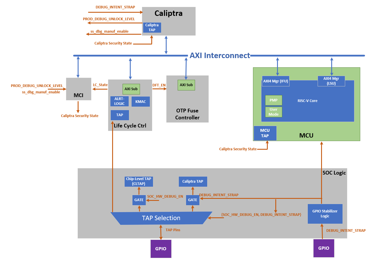 Note: SoC Debug Architecture of the Caliptra Subsystem with LCC; the red dashed circles highlight the newly added blocks and signals.
The figure below shows the LCC state transition and Caliptra Subsystem enhancement on LCC state transitions. It illustrates the life cycle flow of Caliptra Subsystem.
Figure: Caliptra Subsystem Life Cycle Controller Summary
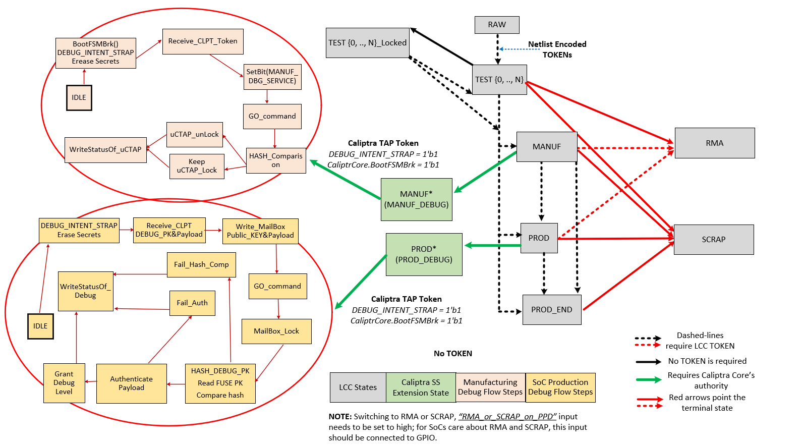
Note: Caliptra Subsystem life cycle flow. This flow shows legal state transitions in life cycle controller by excluding its invalid states for simplicity.
Caliptra Subsystem LCC State Definitions
| Name | Encoding | Description |
|---|---|---|
| RAW | FUSE | This is the default state of the FUSE. During this state, no functions other than transition to TEST_UNLOCKED0 are available. The token authorizing the transition from RAW to TEST_UNLOCKED0 is a value that is secret global to all devices. This is known as the RAW_UNLOCK token. |
| TEST_LOCKED{N} | FUSE | TEST_LOCKED{N} states have identical functionality to RAW state and serve as a way for the Silicon Creator to protect devices in transit. It is not possible to provision FUSE root secrets during this state. This is enforced by hardware and is implementation defined. To progress from a TEST_LOCKED state to another TEST_UNLOCKED state, a TEST_UNLOCKED token is required. |
| TEST_UNLOCKED{N} | FUSE | Transition from RAW state using token stored in FUSE. This state is used for manufacturing and production testing. During this state: CLTAP (chip level TAPs) is enabled; Debug functions are enabled; DFT functions are enabled. It is expected that LCC tokens will be provisioned into FUSE during these states. Once provisioned, these tokens are no longer readable by software. |
| MANUF | FUSE | Transition from TEST_UNLOCKED state using token stored in FUSE. This is a mutually exclusive state to PROD and PROD_END. To enter this state, MANUF_TOKEN is required. This state is used for developing provisioning and mission mode. In this state, UDS and Field Entropy FUSE partitions can be provisioned. During this state: CLTAP (chip level TAPs) is enabled; Debug functions are enabled; DFT functions are disabled |
| PROD | FUSE | Transition from MANUF state using token stored in FUSE. PROD is a mutually exclusive state to MANUF and PROD_END. To enter this state, PROD_TOKEN is required. This state is used both for provisioning and mission mode. During this state: CLTAP is disabled; Debug functions are disabled; DFT functions are disabled; Caliptra Subsytem can grant SoC debug unlock flow if the conditions provided in “SoC Debug Flow and Architecture for Production Mode” section are satisfied. SoC debug unlock overwrites the signals and gives the following cases: CLTAP is enabled; Debug functions are enabled based on the defined debug policy; DFT is enabled but this DFT enable is called SOC_DFT_EN, which has less capabilities than DFT_EN granted in TEST_UNLOCKED. |
| PROD_END | FUSE | This state is identical in functionality to PROD, except the device is never allowed to transition to RMA state. To enter this state, a PROD_END token is required. Only transition to SCRAP mode is allowed. |
| RMA | FUSE | Transition from TEST_UNLOCKED / PROD / MANUF using token stored in FUSE. It is not possible to reach this state from PROD_END. If the RMA transition is requested, the request must follow the asserted RMA PPD pin. Without this pin, RMA request is discarded. See cptra_ss_lc_Allow_RMA_or_SCRAP_on_PPD_i in Caliptra Subsystem Integration Specification Document. When transitioning from PROD or MANUF, an RMA_UNLOCK token is required. When transitioning from TEST_UNLOCKED, no RMA_UNLOCK token is required. During this state: CLTAP is enabled; Debug functions are enabled; DFT functions are enabled |
| SCRAP | FUSE | Transition from any state. If the SCRAP transition is requested, the request must follow the asserted SCRAP PPD pin. Without this pin, SCRAP request is discarded. See cptra_ss_lc_Allow_RMA_or_SCRAP_on_PPD_i in Caliptra Subsystem Integration Specification Document. During SCRAP state the device is completely dead. All functions, including CPU execution are disabled. The only exception is the TAP of the life cycle controller which is always accessible so that the device state can be read out. No owner consent is required to transition to SCRAP. Note also, SCRAP is meant as an EOL manufacturing state. Transition to this state is always purposeful and persistent, it is NOT part of the device’s native security countermeasure to transition to this state. |
| INVALID | FUSE | Invalid is any combination of FUSE values that do not fall in the categories above. It is the “default” state of life cycle when no other conditions match. Functionally, INVALID is identical to SCRAP in that no functions are allowed and no transitions are allowed. A user is not able to explicitly transition into INVALID (unlike SCRAP), instead, INVALID is meant to cover in-field corruptions, failures or active attacks. |
Note
- The LCC performs state transitions in a forward-only manner. It begins in the RAW state and follows the sequence: TEST_UNLOCKED and TEST_LOCKED, then MANUF, then PROD, and finally either PROD_END or RMA. After transitioning to TEST_UNLOCKED, the LCC can branch to any of the following states: MANUF, PROD, PROD_END, or RMA. However, once the LCC transitions to PROD, PROD_END, or RMA, it cannot return to the MANUF state. Additionally, note that the LCC cannot branch to RMA from PROD_END.
DFT & DFD Life-cycle States
In addition to the decoding signals of the Life-Cycle Controller (LCC) proposed in the OpenTitan open-source silicon Root of Trust (RoT) project, we introduce new signals: SOC_DFT_EN as SOC_HW_DEBUG_EN. These signals are critical for managing the test and debug interfaces within the Caliptra Subsystem, as well as at the broader SoC level.
While this architecture document explains how the Caliptra Subsystem provides DFT and DFD mechanisms through the DFT_EN, SOC_HW_DEBUG_EN, and SOC_DFT_EN signals, it also offers greater flexibility by supporting various SoC debugging options through the broader SoC debug infrastructure. The architecture does not constrain the SoC’s flexibility with the core security states of Caliptra and LCC states. We establish a set of clear guidelines for how the Caliptra Subsystem transitions through the unprovisioned, manufacturing, and production phases, ensuring security. However, this architecture remains flexible, offering multiple levels of debugging options in production debug mode. Level 0 is designated for debugging the Caliptra Subsystem itself, while higher levels can be interpreted and customized by the SoC designer to implement additional debugging features. For instance, if the SoC designer wishes to include extra DFT and DFD capabilities, they can utilize one of the debug levels provided during production debug mode and expand its functionality accordingly. For more details, see “SoC Debug Flow and Architecture for Production Mode” Section and “Masking Logic for Debugging Features in Production Debug Mode” Section.
The DFT_EN signal is designed to control the scan capabilities of both the Caliptra Subsystem and the SoC. When DFT_EN is set to HIGH, it enables the scan chains and other Design for Testability (DFT) features across the system, allowing for thorough testing of the chip. This signal is already provided by the existing LCC module, ensuring compatibility with current test structures. However, the SoC integrator has the flexibility to assign additional functionality to one of the debugging options provided by the debug level signals during production debug mode. For example, at the SoC level, an integrator may choose to use one of these levels to enable broader SoC DFT features, allowing for system-level testing while maintaining Caliptra's protection. To enable SoC DFT signal, SoC needs to set SOC_DFT_EN signal HIGH by using the infrastructure defined in “Masking Logic for Debugging Features in Production Debug Mode” Section. Note that SOC_DFT_EN has a different capabilities than DFT_EN signal. DFT_EN is contolled by LCC, while SOC_DFT_EN is controlled by MCI.
The SOC_HW_DEBUG_EN signal is a new addition that governs the availability of the Chip-level TAP (CLTAP). CLTAP provides a hardware debug interface at the SoC level, and it is accessible when SOC_HW_DEBUG_EN is set to HIGH. For further details on how this signal integrates with the overall system, refer to the “TAP Pin Muxing” Section of this document.
In the manufacturing phase, the Caliptra Subsystem asserts SOC_HW_DEBUG_EN high, with the signal being controlled by the LCC. In PROD mode, this signal is low. However, the SoC integrator has the flexibility to enable CLTAP during production debug mode by incorporating additional logic, such as an OR gate, to override the SOC_HW_DEBUG_EN signal, like DFT_EN. This architecture provides a mask register that allows SoC to program/configure this overriding mechanism at integration time or using MCU ROM. This allows the SoC to maintain control over hardware debug access while preserving the intended security protections in production.
Table: LCC State and State Decoder output ports
LCC State and State Decoder Output Ports
| LCC State\Decoder Output | DFT_EN | SOC_DFT_EN | SOC_HW_DEBUG_EN |
|---|---|---|---|
| RAW | Low | Low | Low |
| TEST_LOCKED | Low | Low | Low |
| TEST_UNLOCKED | High | High | High |
| MANUF* | Low | TOKEN - CONDITIONED** | High |
| PROD* | Low | TOKEN - CONDITIONED** | TOKEN - CONDITIONED** |
| PROD_END | Low | Low | Low |
| PROD_END* | Low | TOKEN - CONDITIONED** | TOKEN - CONDITIONED** |
| RMA | High*** | High | High |
| SCRAP | Low | Low | Low |
| INVALID | Low | Low | Low |
| POST_TRANSITION | Low | Low | Low |
*: Caliptra can enter debug mode and update these signals even though LCC is in MANUF or PROD, PROD_END states. This case is explained in “How does Caliptra Subsystem enable manufacturing debug mode?” and “SoC Debug Flow and Architecture for Production Mode”.
**: SOC_DFT_EN and SOC_HW_DEBUG_EN can be high if Caliptra SS grants debug mode (either manufacturing or production). This case is explained in “How does Caliptra Subsystem enable manufacturing debug mode?” and “SoC Debug Flow and Architecture for Production Mode”. SOC_HW_DEBUG_EN is set high to open CLTAP and SOC_DFT_EN enables DFT by SoC design support. However, this condition also needs to go through the flow described in “SoC Debug Flow and Architecture for Production Mode”. Caliptra Subsystem state should be set to either the manufacturing mode debug unlock or Level 0 of the production debug unlock.
***: RMA state enables DFT_EN but Caliptra Core enters the debug mode when LCC enters RMA state. Thus, Caliptra Core clears UDS and Field Entropy secrets.
TAP Pin Muxing
The LCC includes a TAP interface, which operates on its own dedicated clock and is used for injecting tokens into the LCC. Notably, the LCC TAP interface remains accessible in all life cycle states, providing a consistent entry point for test and debug operations. This TAP interface can be driven by either the TAP GPIO pins or internal chip-level wires, depending on the system's current configuration.
Figure: Caliptra Subsystem Life Cycle Controller Summary
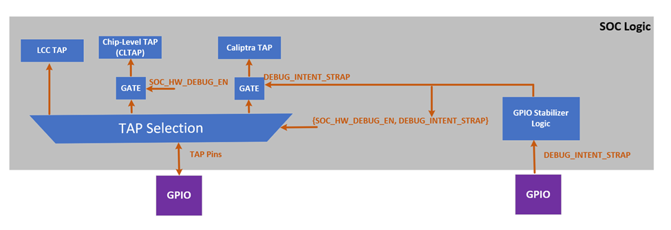 Note: Above figure of TAP pin muxing block diagram with a conceptual representation. SOCs may implement this in their own way
SOC logic incorporates the TAP pin muxing to provide the integration support and manage the connection between the TAP GPIO pins and the Chip-Level TAP (CLTAP). As illustrated in figure above, this muxing logic determines the source that drives the LCC TAP interface. The selection between these two sources is controlled by the SOC_HW_DEBUG_EN signal. When SOC_HW_DEBUG_EN is set to high, control is handed over to the CLTAP, allowing for chip-level debug access through the TAP GPIO pins. Conversely, when SOC_HW_DEBUG_EN is low, the TAP GPIO pins take control, enabling external access to the LCC TAP interface.
LCC State and State Decoder Output Ports Table outlines the specific LCC states that enable the SOC_HW_DEBUG_EN signal. These states include TEST_UNLOCK, MANUF, PROD (debug unlocked version only), and RMA. In these states, the LCC allows internal chip-level debug access via CLTAP, thereby facilitating advanced debugging capabilities. This muxing approach ensures that the TAP interface is appropriately secured, and that access is granted only under specific conditions, aligning with the overall security and functional requirements of the Caliptra Subsystem. Note: It is important to note that CLTAP provides access to the TAP interfaces of the LCC, MCU, or Caliptra Core. This functionality is managed by SoC logic, not by Caliptra-SS. Consequently, the SoC integration effort should ideally include an additional mux after CTAP to route the connection to one of the following: the LCC TAP, MCU TAP, or Caliptra Core TAP.
TAP pin muxing also enables routing to Caliptra TAP. This selection happens when DEBUG_INTENT_STRAP is high. This selection is done through the GPIO and indicates that Caliptra will enter debug mode if the secret tokens are provided. Caliptra Subsystem has two debug modes: manufacturing debug and production debug. Entering these debug flows are explained in the following sections: How does Caliptra Subsystem enable manufacturing debug mode?, SoC Debug Flow and Architecture for Production Mode and Masking Logic for Debugging Features in Production Debug Mode
Note: The Caliptra TAP can run exact flow with AXI, targeting the mailbox and SOC provides that interface to platform.
How does Caliptra Subsystem enable manufacturing debug mode?
The following figure illustrates how Caliptra Subsystem enters the manufacturing debug mode. To enter this mode, LCC should be in MANUF state. While being in manufacturing debug mode, LCC does not change its state from MANUF to any other state. During the MANUF state, Caliptra Subsystem can enable manufacturing debug flow by following steps:
Figure: Caliptra Subsystem Manuf Debug Life Cycle View
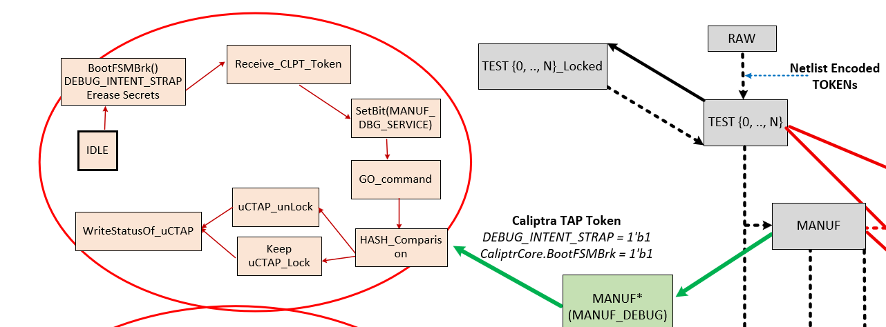 Note: The flow diagram on the right side shows the LCC states (grey boxes) and their transitions, while the flow diagram on the left illustrates Caliptra SS’s enhancements to the LCC for the manufacturing phase. Specifically, the flow on the left depicts the routine for entering manufacturing debug mode.
Flow Explanation
- (Platform) Assert BootFSMBrk : Temporarily halting the Caliptra HW bootfsm boot process to allow for secure operations like token injection and verification.
- (Platform) Assert DEBUG_INTENT_STRAP: If Caliptra core HW samples this pin as high and sees that LCC is in MANUF mode, it prepares itself for entering debug mode. Once the DEBUG_INTENT_STRAP is detected, Caliptra HW immediately wipes out its secret assets, including the Unique Device Secret (UDS) and Field entropy, ensuring that no sensitive data remains accessible. If this Pin is not high, Caliptra continues always in non-debug mode without taking any further action listed with the following states.
- (Platform over TAP) MANUF_DEBUG_UNLOCK_REQ: The system intends to be in debug mode for manufacturing services.
- (Platform over TAP) Write to Boot Continue: Resuming the boot process after halting it with BootFSMBrk.
- ROM reads MANUF_DEBUG_UNLOCK_REQ at optimal time for ROM and clears mailbox lock and asserts MANUF_DEBUG_UNLOCK_IN_PROGRESS.
- Platform over TAP requests Caliptra mailbox lock. If lock is obtained, then platform over TAP writes to TAP mailbox to inject Token via TAP Register Write: Enabling the injection of a token through TAP and writing to a specific register.
- ROM Executes Hash Hashing: Calculates the hash value of the injected token using a SHA-512 hash core. Before starting this operation.
- Token Comparison: A constant-time comparison between the authentication values of injected token and the FUSE content.
- ROM Drives MANUF_DEBUG_UNLOCK Signal: The ROM writes to a register that controls the MANUF_DEBUG_UNLOCK signal based on the result of the token verification.
Note: The manufacturing debug flow relies on the hash comparison hardness rather than an authentication check provided with an asymmetric cryptography scheme. However, the following sections show that production debug flow relies on asymmetric cryptography scheme hardness. The reason behind this choice is that the manufacturing phase is the early phase of the delivery, and this phase is entered in an authorized entity’s facility. Therefore, this architecture keeps the manufacturing phase simpler.
Production Debug Unlock Architecture
The Caliptra Subsystem includes SoC debugger logic that supports Caliptra’s production debug mode. This debugger logic extends the capabilities of the Lifecycle Controller (LCC) by providing a production debug mode architecture that the LCC does not inherently support, except in the RMA state. This architecture manages the initiation and handling of the production debug mode separately from the LCC's lifecycle states.
The process of enabling production debug mode begins when the DEBUG_INTENT_STRAP pin is asserted high via the SoC’s GPIO. This pin signals Caliptra to start the debug mode when the LCC is in the PROD and PROD_END states. Before the debug unlock flow, the MCU reads all hashed public keys from the fuse macros and writes them to the SS_PROD_DEBUG_UNLOCK_AUTH_PK_HASH_REG_BANK registers. Additionally, the MCU sets the number of public keys used for production debug unlock by writing to the SS_NUM_OF_PROD_DEBUG_UNLOCK_AUTH_PK_HASHES register. The value DEBUG_AUTH_PK_HASH_REG_BANK_OFFSET represents an address offset, while NUM_OF_DEBUG_AUTH_PK_HASHES defines how many public keys are available for reading. These two values establish the debug policy depth for different debugging levels.
Overview of Debug Unlock Initiation
The process begins when the platform sets three conditions:
- The
DEBUG_INTENTfield in theSS_DEBUG_INTENTregister. - The
PROD_DEBUG_UNLOCK_REQbit in theSS_DBG_MANUF_SERVICE_REG_REQregister. - The
CPTRA_BOOT_GOallows Caliptra Core to continue its execution. On reset, the Caliptra ROM checks these two signals. If both are asserted, the ROM begins the production debug unlock process. Upon detecting a valid debug intent: - Caliptra hardware erases its secret assets, including the Unique Device Secret (UDS) and Field Entropy, before exposing any debug interfaces, ensuring sensitive data is irreversibly destroyed.
- Caliptra ROM sets the
TAP_MAILBOX_AVAILABLEandPROD_DBG_UNLOCK_IN_PROGRESSbits in theSS_DBG_MANUF_SERVICE_REG_RSPregister.
Note: Similar to the manufacturing debug flow, BootFSMBrk must be asserted to halt Caliptra ROM execution. Otherwise, the ROM may advance past the debug request before PROD_DEBUG_UNLOCK_REQ is populated. BootFSMBrk is a prerequisite for entering the debug flow ONLY if Caliptra core ROM needs to be debugged; for run-time injection of prod debug unlock token, setting BootFSMBrk is not required.
Secure Debug Unlock Protocol
- The production debug unlock flow uses a challenge-response authentication model involving public key verification and hybrid cryptography (ECC and MLDSA). The flow includes the following steps:
- AUTH_DEBUG_UNLOCK_REQ Command: Caliptra ROM polls the Mailbox interface, awaiting an
AUTH_DEBUG_UNLOCK_REQfrom the platform. - The request payload includes:
- AUTH_DEBUG_UNLOCK_REQ Command: Caliptra ROM polls the Mailbox interface, awaiting an
| Field | Size (bytes) | Description |
|---|---|---|
| Length | 4 | Must be 2 DWORDs. |
| Unlock Level | 1 | Requested unlock level. |
| Reserved | 3 | Reserved. |
- If the payload is invalid, Caliptra ROM:
- Sets the
PROD_DBG_UNLOCK_FAILbit. - Clears the
PROD_DBG_UNLOCK_IN_PROGRESSbit. - Exits the debug unlock process.
- Sets the
- Upon successful initial validation, Caliptra ROM sends back an
AUTH_DEBUG_UNLOCK_CHALLENGEpayload:
| Field | Size (bytes) | Description |
|---|---|---|
| Length | 4 | Should be 21 DWORDs. |
| Unique Device Identifier | 32 | Caliptra device identifier. |
| Challenge | 48 | Randomly generated nonce. |
- The platform signs the challenge data and sends an
AUTH_DEBUG_UNLOCK_TOKEN:
| Field | Size (bytes) | Description |
|---|---|---|
| Length | 4 | Should be 0x753 DWORDs. |
| Unique Device Identifier | 32 | Echoed from challenge. |
| Unlock Level | 1 | Echoed from initial request. |
| Reserved | 3 | Reserved. |
| Challenge | 48 | Echoed from challenge. |
| ECC Public Key | 96 | P-384 public key. |
| MLDSA Public Key | 2592 | MLDSA-87 public key. |
| ECC Signature | 96 | Signature of challenge message. |
| MLDSA Signature | 4628 | Signature of challenge message. |
- Finally, Caliptra ROM reads the expected SHA2-384 public key hash from the corresponding register by using the following equation:
- SS_PROD_DEBUG_UNLOCK_AUTH_PK_HASH_REG_BANK_OFFSET + ((Unlock Level - 1) * 48 bytes)
- If hash of
AUTH_DEBUG_UNLOCK_CHALLENGE's MLDSA and ECC public keys match with the read value fromSS_PROD_DEBUG_UNLOCK_AUTH_PK_HASH_REG_BANK_OFFSET, ROM uses these MLDSA and ECC public keys to perform the authentication. - Upon successful validation:
- Sets the
PROD_DBG_UNLOCK_SUCCESSbit. - Writes the
CALIPTRA_SS_SOC_DEBUG_UNLOCK_LEVELregister granted debug level with a one-hot encoding result (1 << (Unlock Level - 1)). - Clears the
TAP_MAILBOX_AVAILABLEbit. - Clears the
PROD_DBG_UNLOCK_IN_PROGRESSbit. - Exits the debug unlock process.
- Sets the
Granting Production Debug Mode:
- If authentication succeeds, Caliptra ROM does not immediately grant full production debug mode. Instead, the ROM sets the appropriate "debug level" signal, which corresponds to the type of debug access being requested.
- Caliptra ROM writes CALIPTRA_SS_SOC_DEBUG_UNLOCK_LEVEL register, which will be wired to the specific debug enable signal. This signal is part of an N-wide signal that is mapped to the payload encoding received during the debug request. N is defined by NUM_OF_DEBUG_AUTH_PK_HASHES. The default version of N is 8. The payload encoding can either be one-hot encoded or a general encoded format, and this signal is passed to the SoC to allow it to make the final decision about the level of debug access that should be granted. In Caliptra’s subsystem-specific implementation, the logic is configured to handle one-hot encoding for these 8 bits. The level 0 bit is routed to both Caliptra and the MCU TAP interface, allowing them to unlock based on this level of debug access. This granular approach ensures that the system can selectively unlock different levels of debugging capability, depending on the payload and the authorization level provided by the debugger.
Granting Production Debug Mode with Caliptra Runtime FW: Although the flow above describes ROM-based authentication, the same challenge–response mechanism may be executed by Caliptra Runtime Firmware. In this case, RT FW performs the challenge-response authentication steps via mailbox commands, which will be used to update the debug unlock level. The DEBUG_INTENT_STRAP must still be asserted high before Caliptra subsystem is out of reset. This ensures that even RT-based debug enablement remains gated by hardware intent and cannot be triggered purely through software.
Masking Logic for Debugging Features in Production Debug Mode (MCI)
In the production debug mode, the SoC can enable certain debugging features—such as DFT_EN and SOC_HW_DEBUG_EN—using a masking mechanism implemented within the Manufacturer Control Interface (MCI). This masking infrastructure allows the SoC to selectively control debug features that are normally gated by Caliptra’s internal signals. The masking logic functions as a set of registers, implemented in the MCI, that can be written by the SoC to override or enable specific debugging functionalities in production debug mode. The masking registers in the MCI act as an OR gate with the existing debug signals. For instance, if DFT_EN is controlled by Caliptra, the SoC can assert the corresponding mask register to enable Design for Test (DFT) capabilities in the SoC, even if Caliptra has not explicitly enabled it. Similarly, the SOC_HW_DEBUG_EN signal can be masked through the MCI registers, giving the SoC the flexibility to unlock TAP interfaces and provide the required debugging in production.
Figure: Caliptra Subsystem Infrastructure for SOC flexibility to override various debug signals
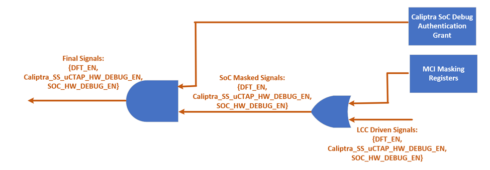
This mechanism is only authorized when both the LCC and Caliptra core are in the PROD state and operating in production debug mode. The masking logic ensures that these features are enabled securely, in line with the production debug flow described in the "SoC Debug Flow and Architecture for Production Mode" section. By leveraging the MCI’s masking infrastructure, the SoC integrator has greater flexibility to implement custom debugging options during production without compromising the security framework established by Caliptra.
**Note: Unlike the production state, the manufacturing state supports only a single debug level. Although it uses the same masking register to override DFT_EN, only the register’s least significant bit is used in manufacturing debug mode.
LCC Interpretation for Caliptra “Core” Security States
Caliptra Core has five security states as given with the figure below (Copied from Caliptra core specification). Three of these states enable debugging with different features, while two of these states are in non-debug mode. Caliptra Subsystem implements gasket logic to translate the LCC states to Caliptra “Core” security states.
Figure: Caliptra Core Security States

This translation is essential for ensuring that the system behaves correctly according to its current lifecycle stage, whether it is in a development phase, production, or end-of-life states. The LCC provides specific decoding signals—DFT_EN, SOC_DFT_EN, SOC_HW_DEBUG_EN—that accommodates the debug capabilities and security states of the Caliptra Core. Depending on the values of these signals, the Caliptra Core transitions between different security states as follows:
Non-Debug Mode: This state is enforced when the LCC is in RAW, TEST_LOCKED, SCRAP, INVALID, or POST_TRANSITION states. In these states, the DFT_EN, SOC_DFT_EN, SOC_HW_DEBUG_EN signals are all low, ensuring that no debug functionality is available. Caliptra remains in a secure, non-debug state, with no access to debugging interfaces.
Unprovisioned Debug Mode: When the LCC is in the TEST_UNLOCKED state, the DFT_EN, SOC_DFT_EN, SOC_HW_DEBUG_EN signals are all set high, enabling debug functionality. In this mode, the Caliptra Core allows extensive debugging capabilities, which is typically used during early development and bring-up phases.
Manufacturing Non-Debug Mode: This state occurs when the LCC is in the MANUF state, with SOC_HW_DEBUG_EN high and DFT_EN and SOC_DFT_EN low. In this state, the secrets have been programmed into the system, and the Caliptra can generate CSR (Certificate Signing Request) upon request. However, it remains in a secure, non-debug mode to prevent reading secrets through the debugging interfaces.
Manufacturing Debug Mode: Also occurring in the MANUF state, this mode is enabled when SOC_HW_DEBUG_EN is high. Here, the Caliptra Core provides debugging capabilities while maintaining security measures suitable for manufacturing environments. In this state, DFT_EN is low. However, SOC_DFT_EN can be set high if LSB of MCI_REG_SOC_DFT_EN_0 is set to high in MANUF debug state MCI-LCC-Signal-Masking.
Production Non-Debug Mode: This state is active when the LCC is in the PROD or PROD_END states, with all debug signals (DFT_EN, SOC_HW_DEBUG_EN) set to low. The Caliptra Core operates in a secure mode with no debug access, suitable for fully deployed production environments.
Production Debug Mode: This state is active when the LCC is in the PROD or PROD_END states, with debug DFT_EN, SOC_HW_DEBUG_EN set to low. Caliptra Core provides debugging capabilities while maintaining security measures suitable for manufacturing environments. However, SOC_DFT_EN and SOC_HW_DEBUG_EN can be set high with MCI masking registers MCI-LCC-Signal-Masking.
Production Debug Mode in RMA: In the RMA state, all debug signals are set high, allowing full debugging access. This state is typically used for end-of-life scenarios where detailed inspection of the system's operation is required.
The table below summarizes the relationship between the LCC state, the decoder output signals, and the resulting Caliptra “Core” security state:
Table: LCC state translation to Caliptra "Core" security states
| LCC State vs Decoder Output | DFT_EN | SOC_DFT_EN | SOC_HW_DEBUG_EN | Caliptra “Core” Security States |
|---|---|---|---|---|
| RAW | Low | Low | Low | Prod Non-Debug |
| TEST_LOCKED | Low | Low | Low | Prod Non-Debug |
| TEST_UNLOCKED | High | High | High | Unprovisioned Debug |
| MANUF | Low | Low | High | Manuf Non-Debug |
| MANUF* | Low | High** | High | Manuf Debug |
| PROD | Low | Low | Low | Prod Non-Debug |
| PROD* | Low | High** | High** | Prod Debug |
| PROD_END | Low | Low | Low | Prod Non-Debug |
| PROD_END* | Low | High** | High** | Prod Debug |
| RMA | High | High | High | Prod Debug |
| SCRAP | Low | Low | Low | Prod Non-Debug |
| INVALID | Low | Low | Low | Prod Non-Debug |
Note: In RAW, TEST_LOCKED, SCRAP and INVALID states, Caliptra “Core” is not brought out of reset. *: These states are Caliptra SS’s extension to LCC. Although the LCC is in either MANUF or PROD, PROD_END states, Caliptra core can grant debug mode through the logics explained in “How does Caliptra Subsystem enable manufacturing debug mode?” and “SoC Debug Flow and Architecture for Production Mode”. **: SOC_HW_DEBUG_EN and DFT_EN can be overridden by SoC support in debug mode of MANUF and PROD, PROD_END states.
Exception: Non-Volatile Debugging Infrastructure and Initial RAW State Operations
The Caliptra Subsystem features a non-volatile debugging infrastructure that allows the SoC integrator to utilize a dedicated SRAM for early-stage debugging during the VolatileUnlock state. This SRAM provides a means to store executable content for the MCU, enabling early manufacturing debug operations.
It is important to note that the VolatileUnlock state is not a standard LCC state but rather a temporary state. Unlike other LCC states, the LCC can transition to this state without requiring a power cycle, provided the necessary global VolatileUnlock token is passed. This token is unique in that it is not stored in the FUSE partition but is instead a global netlist secret.
Once in the VolatileUnlock state, the MCU can execute instructions stored in the SRAM, which can be initialized through a backdoor mechanism. This capability allows for basic FUSE tests and calibration operations during early debugging. However, the VolatileUnlock state is inherently unstable and temporary—if a reset is applied or the Caliptra Subsystem undergoes a power cycle, the LCC will return to the RAW state.
LCC RAW Unlock Token Generation & Setting
The hashed RAW unlock token is stored as a netlist constant. Its value is determined by the
cptra_ss_raw_unlock_token_hashed_i input of caliptra_ss_top. Every integrator must set the
hashed token to a unique value. tools/scripts/lc_ctrl_script/gen_lc_ctrl_token.py can be used to
generate the hashed token. The unhashed RAW unlock token is a secret that must be obtained from
a cryptographically secure random number generator. The aforementioned tool accepts an unhashed
token as input or, if omitted, generates an unhashed token using Python's secrets module.
The hashed RAW unlock token must be applied to the cptra_ss_raw_unlock_token_hashed_i input of
caliptra_ss_top. It's also required in SW that performs a volatile RAW unlock.
The unhashed RAW unlock token is required in SW that performs a non-volatile RAW unlock.
SOC LCC Interface usage & requirements
The interaction between the SoC and the LCC within the Caliptra Subsystem is pivotal for maintaining the security and functionality of the overall system. This section outlines the specific usage and requirements for interfacing with the LCC from the SoC perspective.
SOC_HW_DEBUG_EN Utilization: The SOC_HW_DEBUG_EN signal plays a crucial role in controlling access to the Chip-Level TAP (CLTAP). When SOC_HW_DEBUG_EN is asserted high, it enables the exposure of registers to the TAP interface that are deemed secure for access during debugging. This is particularly important when CLTAP is open, as it allows authorized debugging operations while ensuring that sensitive or secure information remains protected.
LCC Outputs for Security/Debug Purposes: Beyond the primary debug controls, all other LCC outputs, as listed in the signal table below, are available for use by the SoC for any security or debugging purposes. These outputs provide the SoC with additional control signals that can be leveraged to enhance system security, monitor debug operations, or implement custom security features.
Integration with Clock/Voltage Monitoring Logic: If the SoC includes clock or voltage monitoring logic, it is recommended that these components be connected to the LCC's escalation interface. By integrating with the LCC, the SoC can ensure that any detected anomalies, such as voltage fluctuations or clock inconsistencies, trigger appropriate secure transitions as defined in this document. This connection enhances the overall security posture by enabling the LCC to respond dynamically to potential threats or system irregularities.
These requirements ensure that the SoC and LCC work in tandem to maintain a secure environment, particularly during debugging and system monitoring. By adhering to these guidelines, the SoC can leverage the LCC’s capabilities to protect sensitive operations and enforce security policies across the system.
LCC Module: Summarized Theory of operation
The LCC is designed to handle the various life-cycle states of the device, from initial provisioning through manufacturing to production and eventual decommissioning (RMA). It provides mechanisms for state transitions, secure key management, and debug control, ensuring that the device operates securely throughout its lifecycle. For more information, please refer to the Life-cycle controller documentation. While the LCC is reused from OpenTitan, Caliptra Subsystem’s security & debug architecture has some differences. Therefore, Subsystem implements the functions required to meet Caliptra specific requirements.
LCC has the same power up sequence as described in Life cycle controller documentation of OpenTitan open-source silicon Root of Trust (RoT) project. After completing the power up sequence, the LCC enters the normal operation routine. During this phase, its output remains static unless specifically requested to change. The LCC accepts life-cycle transition change requests from its TAP interface (TAP Pin Muxing). There are two types of state transitions: (i) unconditional transitions and (ii) conditional transitions.
For unconditional transitions, the LCC advances the state by requesting an FUSE update to the FUSE controller. Once the programming is confirmed, the life cycle controller reports a success to the requesting agent and waits for the device to reboot.
For conditional transitions, the LCC can also branch different states (TEST_UNLOCK, MANUF, PROD, PROD_EN, RMA) based on the received token through the TAP interface and compared the received tokens against the ones stored in FUSE . This branching is called conditional transitions. For more information about the conditional states, please refer to OpenTitan open-source silicon Root of Trust (RoT) project.
Notes:
- Some tokens are hardcoded design constants (specifically for RAW to TEST_UNLOCK), while others are stored in FUSE.
- Conditional transitions will only be allowed if the FUSE partition holding the corresponding token has been provisioned and locked.
- For transition counter limits and token hashing mechanism, please refer to OpenTitan open-source silicon Root of Trust (RoT) project [1].
- The LCC enters the post transition handling routine after completing conditional and unconditional transitions. During this routine, the LCC disables all of its decoded outputs and puts the system in an inert state.
Manufacturer Control Unit (MCU)
MCU is an instance of VeeR EL2 core. The following features are enabled on MCU - iCache, dedicated DCCM, AXI interfaces with seperate AXI USER ID to ROM and MCI, bit manipulation extensions that we have for Caliptra core (Zba, Zbb, Zbc, Zbs) and PMP + SMEPMP with max PMP entries. Please see Caliptra subsystem integration spec for the configuration options available at subsystem level.
If the MCU VeeR instance must be regenerated with new configuration, a shell script is available in the Caliptra Subsystem repository. The script is located at tools/scripts/veer_build_command.sh.
Manufacturer Control Interface (MCI)
Overview
The Manufacturer Control Interface (MCI) is a critical hardware block designed to supplement the Manufacturer Control Unit (MCU) within a System on Chip (SoC). The primary functions of the MCI include providing an SRAM bank, facilitating restricted communication through a mailbox from external entities, and managing a bank of Control/Status Registers (CSRs). Additionally, the MCI incorporates a Watchdog Timer and a Boot Sequencing Finite State Machine (FSM) to manage timing and control during the SoC boot sequence after power application. This boot sequence encompasses reset deassertion, initialization of the Fuse Controller, initialization of the Lifecycle Controller, and enabling the JTAG block for debugging and manufacturing processes.
The following diagram illustrates the internal components of the MCI.
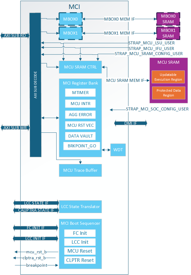
MCI Feature Descriptions
Control/Status Registers (CSRs)
The Control/Status Registers (CSRs) within the MCI are designed to provide critical control and status monitoring functions for the SoC. These registers include configuration settings, status indicators, and control bits that allow communication and management of the various operations of the MCI. The CSR bank is accessible via the AXI interface and is mapped into the memory space to facilitate straightforward access and manipulation.
MCI CSR Access Restrictions
Certain registers within the CSR bank have write access restrictions based off of:
- AXI User
- Lock bits (SS_CONFIG_DONE, CAP_LOCK, etc.)
The privilaged users for the MCI CSRs are:
- MCU
- MCI SOC Config User (MSCU)
- MCU SRAM Config User (MSRCU)
All of these AXI Users come from straps and are not modifiable by SW. MCU is given the highest level of access and is expected to configure MCI registers and lock the configuration with various SS_CONFIG_DONE and LOCK bits. It also has access to certain functionalality like timers that are needed by the SOC but are critical for MCU functionality.
The MSCU is meant as a secondary config agent if the MCU is unable to configure MCI. Example when in the no ROM config it is expected the MCSCU can configure and lock down the MCI configuration. MSCU can be disabled by setting the strap to 0x0. For debug the MSCU strap can be set to all 1s meaning every access will give this level of privilege. The MCRCU populates the MCU FW update in MCU SRAM. There are a few registers within the MCI register bank it has special access to for facilitating the FW update. The registers can be split up into a few different categories:
| Write restrictions | Description |
|---|---|
| MCU Only | These registers are only meant for MCU to have access. There is no reason for SOC or the MCI SOC Config User to access the. Example is the MTIMER |
| MCU or MSCU | Access restricted to trusted agents but not locked. Example:RESET_REQUEST for MCU. |
| MCU or MSRCU | Access restricted to trusted agents but not locked. Example:RESET_REASON for MCU. |
| MCU or MSCU and CONFIG locked | Locked configuration by MCU ROM/MSCU and configured after each warm reset |
| Sticky MCU or MSCU and CONFIG locked | Locked configuration by MCU ROM/MSCU and configured after each cold reset |
| Locked by SS_CONFIG_DONE_STICKY | Configuration once per cold reset. |
| Locked by SS_CONFIG_DONE | Configuration once per warm reset. |
| MCU or MSCU until CAP_LOCK | Configured by a trusted agent to show HW/FW capabilieds then locked until next warm reset |
| MBOX_USER_LOCK | Mailbox specific configuration locked by it's own LOCK bit. Configured afer each arem reset. |
MCI Straps
All MCI straps shall be static before mci_rst_b is deasserted. Some straps have further restrictions as described below.
MCI has the following types of straps:
| Strap Type | Sampled or Direct Use | Description |
|---|---|---|
| Non-configurable Direct | Direct | Used directly by MCI and not sampled at all. These shall be constant non-configurable inputs to CSS/MCI. Inside MCI these are not overridable by SW. |
| Non-configurable Sampled | Sampled* | Sampled once per cold boot and not overridable by SW |
| Configurable Sampled | Sampled** | Sampled once per warm boot and SW can override via MCI Register Bank until SS_CONFIG_DONE is set. |
*NOTE: Strap sampling occurs when mci_rst_b is deasserted and is typically performed once per cold boot. This process is controlled by the SS_CONFIG_DONE_STICKY register; when set, sampling is skipped. If a warm reset happens before SS_CONFIG_DONE_STICKY is set, the straps will be sampled again, although this is not the usual behavior.
**NOTE: Strap sampling occurs when mci_rst_b is deasserted.
| Strap Name | Strap Type | Description |
|---|---|---|
strap_mcu_lsu_axi_user | Non-configurable Direct | MCU Load Store Unit AXI User. Given Special Access within MCI. |
strap_mcu_ifu_axi_user | Non-configurable Direct | MCU Instruction Fetch Unit AXI User. given special access within MCI. |
strap_mcu_sram_config_axi_user | Non-configurable Direct | MCU SRAM Config agent who is given special access to MCU SRAM Execution region to load FW image. Typically set to Caliptra's AXI User. |
strap_mci_soc_config_axi_user | Non-configurable Direct | MCI SOC Config User (MSCU). AXI agent with MCI configuration access. |
strap_mcu_reset_vector | Configurable Sampled | Default MCU reset vector. |
ss_debug_intent | Non-configurable Sampled | Provides some debug access to MCI. Shows the intent to put the part in a debug-unlocked state. This strap is not writable by SW via AXI, and it is read-only over DMI. Debug intent can additionally be asserted by the MCU through the AXI-writable SS_DEBUG_INTENT_MCU register (W1S, settable only before SS_CONFIG_DONE_STICKY); that register is OR'd with this strap to form the effective debug intent. |
Subsystem Boot Finite State Machine (CSS-BootFSM)
The Boot Sequencer FSM is responsible for the orderly and controlled boot process of the Caliptra Subsystem. This state machine ensures that all necessary initialization steps are completed in the correct sequence after power application. The boot sequence includes MCU and Caliptra Reset deassertions, Fuse Controller Initialization, and Lifecycle Controller Initialization.
The following boot flow explains the Caliptra subsystem bootFSM sequence.
Note: SOC may have other HW FSM steps that were done before Caliptra (CSS) is brought out of reset such as locking a PLL or calibrating a CRO, setting up GPIOs, test logic bring up etc. using SOC HW FSM.
-
SOC asserts Caliptra SS powergood and desserts Caliptra SS reset to MCI
a. SOC may choose to connect the same signals to the AXI fabric or bring it out of reset using a different signals. But the requirement is that before MCU is out of reset, fabric should be operational.
-
CSS-BootFSM will sample straps in MCI and will drive its outputs to reset defaults.
c. Note: In allowed LCC states, MCU TAP will be available when MCI is brought out of reset. Uncore registers in MCI will be available, but Core registers within MCU will only be available when MCU reset is deasserted.
-
CSS-BootFSM will go through Caliptra Subsystem Fuse controller (CSS FC) Init Sequence Init Sequence/handshakes
-
CSS-BootFSM will go through Caliptra Subsystem Life Cycle Controller (CSS LCC) Init Sequence/handshakes
a. SOC Note: Note that LCC shall start on an SOC generated internal clock to prevent clock stretch attacks
b. SOC Note: If the life cycle state is in RAW, TEST* or RMA, and if TRANSITION_CTRL.EXT_CLOCK_EN is set to one, the CLK_BYP_REQ signal is asserted in order to switch the main system clock to an external clock signal. This functionality is needed in certain life cycle states where the SOC internal clock source may not be fully calibrated yet, since the FUSE macro requires a stable clock frequency in order to reliably program the fuse array. Note that the TRANSITION_CTRL.EXT_CLOCK_EN register can only be set to one if the transition interface has been claimed via the CLAIM_TRANSITION_IF mutex. This function is not available in production life cycle states.
-
If MCU-No-ROM-Config strap is not set, then CSS-BootFSM will bring MCU out of reset and MCU ROM will start executing.
a. Note: MCU ROM may be used by some SOCs for doing additional SOC specific initializations.An example of such a SoC construction is MCI, MCU, CSS Fabric are running on external clock initially. MCU brings up PLL, some GPIO peripherals, does I3C init sequence etc and then performs clock switch to internal PLL clock domain so that the fabric is running on the internal clock domain before secrets are read on it from the fuse controller.
-
If MCU-No-ROM-Config is not set, MCU ROM will bring Caliptra out of reset by writing a MCI register (CPTRA_BOOT_GO)
-
If MCU-No-ROM-Config is set, CSS-BootFSM waits for a Caliptra GO write from SOC to bring Caliptra out of reset.
a. Note: MCU Reset Vector will be strapped to the MCU SRAM executable location at integration time.
b. Note: MCI will allow "MCI SOC CONFIG" AXI User to configure MCI registers MCU typically configures.
b. Note: MCI will allow any AXI User to write into SRAM if the LCC & debug state allows. SOC will have flexibility to implement desired logic to write to MCU SRAM to skip MCU ROM and a register bit to bring MCU out of reset. MCU will start executing from the reset vector that was strapped which enables the first fetch vector to access MCI SRAM
-
Caliptra reset (cptra_rst_b) is deasserted.
-
Caliptra BootFSM will go through its own boot flow as documented in Caliptra spec, reads secret fuses and sets “ready_for_fuses” to MCI.
Note: In MCU-NO-ROM-CONFIG, steps 11 through 14 & steps 16 through 18 are done by a SOC entity. Otherwise, MCU ROM will do the below steps.
-
MCU ROM will be polling for this indication
-
MCU ROM will now read FC’s SW partition for all the required fuses including its own and also write Caliptra fuses. Note that only non-secret fuses are accessible for MCU ROM by fuse controller construction. a. Note: All fuses will be zero if FC is not programmed
-
MCU ROM will also write owner_pk_hash register (and any other additional pre-ROM configuration writes here)
-
MCU ROM will do a fuse_write_done write to Caliptra
-
Caliptra ROM starts to execute from here on.
-
Once Caliptra populates MCU SRAM, it will set FW_EXEC_CTL[2] which will trigger a reset request to MCU. MCU either needs to enable interrupts or poll on the appropriate bit to detect that Caliptra has requested a reset.
-
CSS-BootFSM waits for MCU to request the reset. Then CSS-BootFSM will do a halt req/ack handshake with MCU and assert the MCU reset after the MCU reports that it has successfully halted.
-
MCU ROM will read the reset reason in the MCI and execute from MCU SRAM
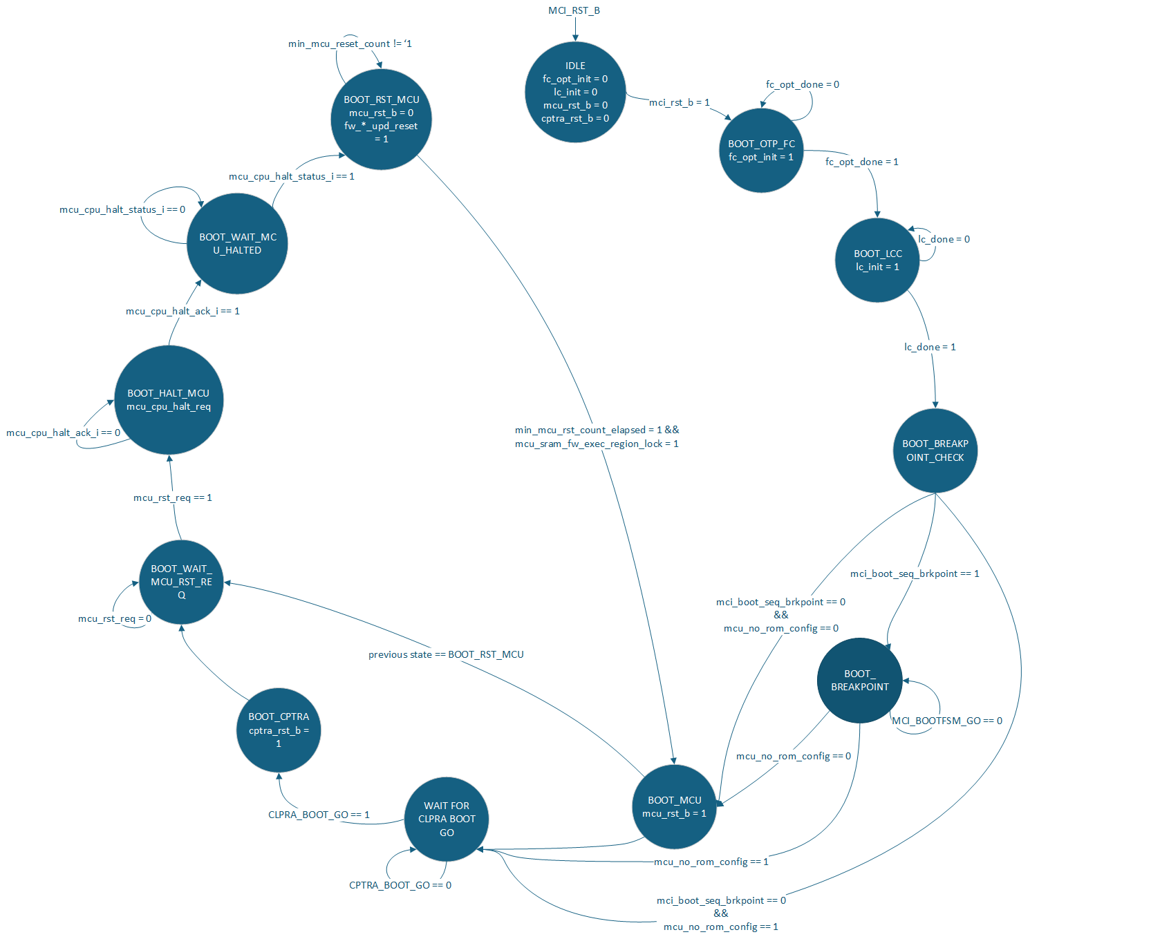
Watchdog Timer
The Watchdog Timer within the MCI is a crucial component designed to enhance the reliability and robustness of the SoC. This timer monitors the operation of the system and can trigger a system reset if it detects that the system is not functioning correctly. The Watchdog Timer is configurable through CSRs and provides various timeout periods and control mechanisms to ensure the system operates within defined parameters. The Watchdog timer contains two different timers. These timers can be configured in two different modes:
- Cascade
- Independent
In cascade mode when the first timer reaches a timeout two things will happen:
- An error interrupt will be triggered
- Timer 2 will start counting
If the WDT is not serviced before Timer 2 times out two things happen:
- NMI output pin is asserted
- NMI HW_ERROR_FATAL is triggered which can assert an error_fatal on the MCI port.
In Independent mode the two timers are completely independent of each other. When they timeout an error interrupt will be asserted. The NMI will never be asserted while in independent mode.
MCU Mailbox
There are 2 mailboxes in the MCI. Each Mailbox component of the MCI allows for secure and restricted communication between external SoC entities and the MCU. This communication channel is essential for exchanging control messages, status updates, and other critical information that the MCU will use to monitor system boot, firmware updates, and security critical operations. Mailboxes are designed to ensure that only authorized entities can access and communicate through it, preserving the integrity and security of the SoC operations.
MCU Mailbox Limited Trusted AXI users
There are 5 trusted AXI Users determined at build time via parameters or via MCI lockable registers. These users, a default user 0xFFFF_FFFF, and MCU are the only AXI users that can access or obtain a lock on the mailbox.
Any untrusted AXI user trying to read or write the mailbox will receive an AXI error response (MCU Mailbox Errors).
Trusted users always have read access to the CSRs in the mailbox, but require a lock to write the CSRs or read/write the SRAM.
MCU Mailbox Locking
A Requester will read the "LOCK" register to obtain a lock on the mailbox. This is a read-set register, the lock is acquired when read returns 0. The Requester must be a Trusted user. Once the lock is obtained the Requestor has read access to the entire mailbox and write access to:
- All mailbox registers except the following will be RO:
- CMD_STATUS
- TARGET_STATUS
- TARGET_DONE
- TARGET_USER
- Mailbox SRAM Unlocking/releasing occurs when the requestor writes 0 to the EXECUTE register. After releasing the mailbox the SRAM is zeroed out(MCU Mailbox SRAM Clearing).
On MCI reset release the MCU MBOX is locked for MCU. The MCU shall set the DLEN to the size of the SRAM and release the MBOX, causing the SRAM to be zeroed. This is done to prevent data leaking between warm resets via the SRAM.
MCU Mailbox Target User
A Target user is an additional user that can access and process the MBOX request. This user can only be setup by MCU and only valid when the TARGET_USER_VALID bit is set.
One example of when a Target user becomes necessary is when the SOC wants Caliptra to process a MBOX request. The SOC will obtain a lock, MCU will see the command request is for Caliptra, MCU will add Caliptra as the Target user and notify Caliptra.
Another example is when MCU itself obtains the mailbox lock. It will add a Target user and notify the Target user via AXI or some other mechanism.
A Target user has read access to the entire mailbox and write access to:
- DLEN register
- TARGET_STATUS register
- TARGET_DONE register
- Mailbox SRAM
The Target user will notify MCU it is done processing by setting TARGET_STATUS and TARGET_DONE. Setting TARGET_DONE will interrupt MCU. If required, MCU will then update the CMD_STATUS register with the final status of the command for the Requestor.
If a second Target user is required it is the MCU's responsibility to:
- Clear TARGET_STATUS
- Clear TARGET_DONE
- Set new TARGET_USER
Otherwise these registers are cleared when the mailbox lock is released.
Target users must be an MCU Mailbox trusted user
MCU Mailbox Fully addressable SRAM
The SRAM is fully addressable and reads are not destructive in this mailbox.
Min Size: 0
Max Size: 2MB
If set to 0 the mailbox is not instantiated.
Accesses must be DWORD aligned and BYTE accesses are not supported by the SRAM.
MCU Mailbox SRAM Clearing
When the mailbox lock is released the SRAM is zeroed out from 0 to max DLEN set during the locking period. The flow for clearing the SRAM is:
- Requester releases lock
- MCU SRAM starts clearing
- MCU SRAM clearing ends
- Mailbox is unlocked
The Requester is locked out of the mailbox after step 1, even though the lock isn't cleared until step 4.
It is expected that agents write their content from 0 to DLEN. If an agent writes outside of this SRAM area, there is no security guarantee for that content because that data would not be zeroized between mailbox operations.
NOTE: When DLEN = 0 the entire MBOX SRAM is cleared.
MCU Mailbox Interrupts
The following interrupts are sent to MCU:
| Interrupt | Description |
|---|---|
| SOC request MBOX | Asserted when MCU has MBOX lock and an SOC agent tries to obtain the lock. MCU can decide to release the mailbox if this happens. |
| Mailbox data available from SOC | Asserted when a SOC agent gets lock and assert the EXECUTE register, indicating data is availalbe for MCU. |
| Target Done | Asserted when the Target user is done processing the data and is ready for MCU to consume or pass data to Requestor. |
The following interrup(s) are available for SOC consumption:
| Interrupt | Description |
|---|---|
| Mailbox data available from MCU | Asserted when MCU gets lock and assert the EXECUTE register, indicating data is available for SOC consumption. |
MCU Mailbox Errors
Each mailbox has the following errors:
| Error Type | Response | Description |
|---|---|---|
| Untrusted User Access | Read: - Data return 0 - AXI Error Write: - Data dropped - AXI Error | When an Untrusted user tries to access any address within the MBOX. |
| Trusted User Illegal Access | Read: - Data return 0 Write: - Data dropped | When a Trusted user tries to: - Access the mailbox when it doesn't have a lock - Tries to write to a register it doesn't have access to. - Tries to access an illegal SRAM address within the mailbox. |
| Single Bit ECC Error | - Interrupt to MCU - Mailbox ECC SB status set - Data corrected | Single bit ECC error while reading Mailbox. |
| Double Bit ECC Error | - Error interrupt to MCU - HW_NON_FATAL error set for SOC consumption - Mailbox ECC DB status set - Invalid data returned | Double bit ECC error while reading Mailbox. |
Whenever an agent reads data from the SRAM they either need to consume the Double Bit ECC interrupt wire or check the MCU Mailbox status registers to know if the data they received is valid.
MCU Mailbox MCU Access
When there is a mailbox lock the MCU has full access to the mailbox CSRs and SRAM in order to facilitage interactions and help with any lockup.
It is the only agent allowed to set TARGET_USER and update the final CMD_STATUS.
MCU Mailbox Address Map
| Start Address | End Address | Name | Description |
|---|---|---|---|
| 0x0000_0000 | 0x01F_FFFF* | MBOX SRAM | Mailbox SRAM |
| 0x0020_0000 | 0x020_003F | MBOX CSR | Mailbox Control Status Registers |
*NOTE: MBOX SRAM size is configurable, but MBOX always reserves 2MB address space. See MCU Mailbox Errors for how access to and invalid SRAM address are handled.
MCU SRAM
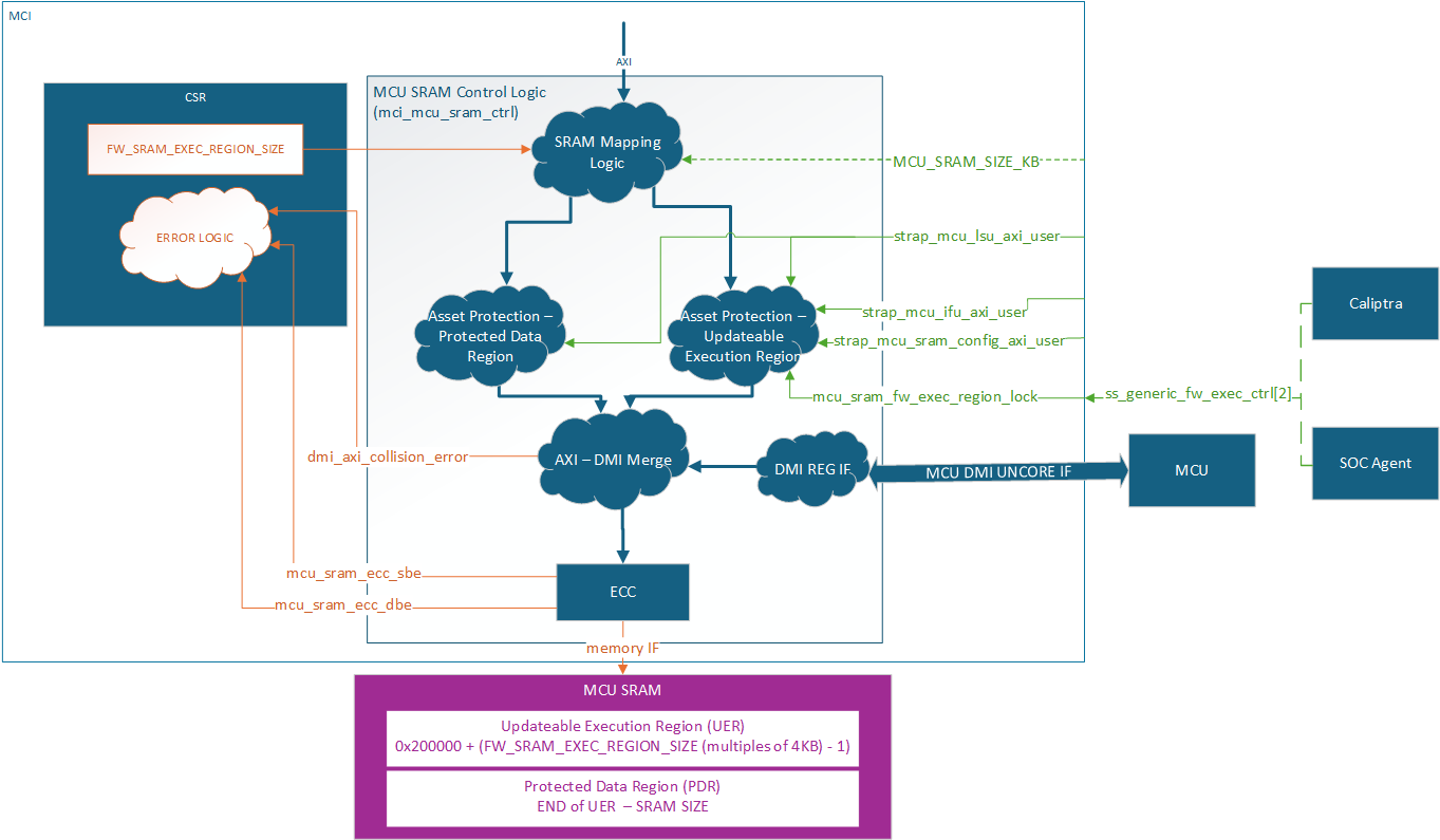
The MCU SRAM provides essential data and instruction memory for the Manufacturer Control Unit. This SRAM bank is utilized by the MCU to load firmware images, store application data structures, and create a runtime stack. The SRAM is accessible via the AXI interface and is mapped into the MCI's memory space for easy access and management. Exposing this SRAM via a restricted API through the SoC AXI interconnect enables seamless and secured Firmware Updates to be managed by Caliptra.
Min Size: 4KB
Max Size: 2MB
AXI USER filtering is used to restrict access within the MCU SRAM based on system state and accessor. Access permissions are based on the AXI USER input straps (either the MCU SRAM Config AXI_USER, or the MCU IFU/LSU AXI USERS). Any write attempt by an invalid AXI_USER is discarded and returns an error status. Any read attempt returns 0 data and an error status. The MCU SRAM contains two regions, a Protected Data Region and an Updatable Execution Region, each with a different set of access rules.
After each MCU reset the Updateable Execution Region may only be read/written by MCU SRAM Config User (typically Caliptra) prior to mcu_sram_fw_exec_region_lock input signal is set. Once fw_exec_region_lock is set it can be read/written by the MCU IFU or MCU LSU until MCU reset is asserted.
The Protected Data Region is only ever read/write accessible by MCU LSU. The span of each region is dynamically defined by the MCU ROM during boot up. Once MCU has switched to running Runtime Firmware, the RAM sizing shall be locked until any SoC-level reset. ROM uses the register FW_SRAM_EXEC_REGION_SIZE to configure the SRAM allocation in 4KB increments. FW_SRAM_EXEC_REGION_SIZE counts in base 0 meaning the smallest the Updateable Execution Region size can be is 4KB. It is possible for the entire SRAM to be allocated to the Updatable Execution Region and there be no Protected Data Region.
The entire MCU SRAM has ECC protection with no ability to disable. Single bit errors are detected and corrected. Double bit errors are detected and error.
MCI actions for single bit errors:
- Correct data and pass corrected data back to the initiator.
- Send maskable interrupt notification to MCU.
MCI actions for double bit errors:
- AXI SLVERR response to the initiator
- HW_ERROR_FATAL asserted and sent to SOC
MCU SRAM is accessible via DMI, see DMI MCU SRAM Access for more details.
MCU Hitless Update Handshake
The hitless flow is described in full in Caliptra Top Spec. The Caliptra SS Integration Spec contains all MCI warm reset and hitless update flows and restrictions. This section is focused on the HW registers both Caliptra and MCU will used to complete the flow.
MCI tracks three different RESET_REASON in its register bank:
| Reset type | Description |
|---|---|
WARM_RESET | MCI reset cycle. MCU SRAM has FW image but need Caliptra interaction before jumping to the FW image. |
FW_BOOT_UPD_RESET | First hitless update since MCI warm reset. MCU SRAM needs full initialization. |
FW_HITLESS_UPD_RESET | Second or greater hitless update since MCI warm reset. MCU SRAM can be partially initialized since valid content still exists in the MCU SRAM from previous firmware. |
WARM_RESET will be set by hardware when a warm reset occurs. It should be cleared by the Caliptra Core during a firmware boot or hitless update flow.
FW_BOOT_UPD_RESET and FW_HITLESS_UPD_RESET are typically set and cleared by the Caliptra Core during a firmware boot or hitless update flow. If Caliptra Core is not used in the design, the SoC needs to designate a different trusted entity to control these registers.
FW_EXEC_CTLR[2] is an input signal to the MCI and is sent as an interrupt (notif_cptra_mcu_reset_req_sts) to the MCU. This interrupt should be cleared by the MCU before it requests a reset with RESET_REQUEST.req. After a warm reset, setting FW_EXEC_CTRL[2] will trigger an interrupt to the MCU, indicating that the MCU should reset itself with RESET_REQUEST.req. After the first MCU reset request, when this input signal is cleared, it triggers the interrupt. The MCU is held in reset until FW_EXEC_CTRL[2] is set, with a minimum reset time determined by the MIN_MCU_RST_COUNTER MCI parameter.
MCI AXI Subordinate
MCI AXI Subordinate decodes the incoming AXI transaction and passes it onto the appropriate submodule within MCI.
The MCI AXI Sub will respond with an AXI error if one of the following conditions is met:
- Submodule error response
AXI access misses are:
- Writes dropped
- Reads return 0
MCI Interrupts
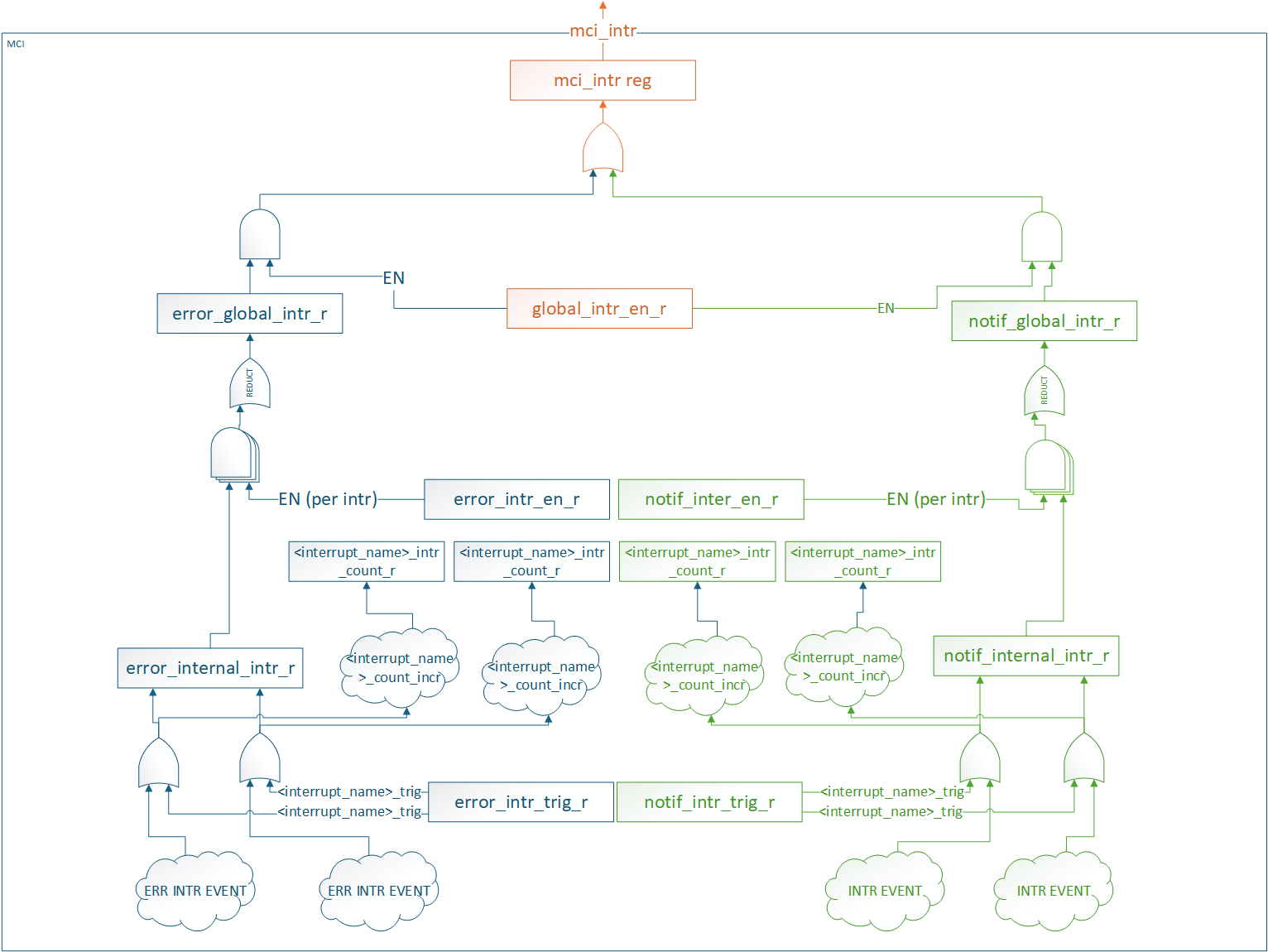
All interrupt status and control registers live in the CSR block. Each interrupt has the following properties:
- Status: W1C for SW to clear
- Enable: Prevents status from propagating. It does not block the status from being set.
- SW Trigger: Ability for SW to manually trigger the interrupt. Typically used for debug.
- Counter: Counts number of times the interrupt event was detected (SW or HW).
There are two different groups of interrupts
- Error
- Notification
Each group of interrupts has its own global status and enable registers that are an aggregate of all interrupts in the group. These status and enable registers have the same properties as the individual interrupt status and enable registers.
All interrupt groups are ORed and sent out on a signal mci_intr pin.
SW access to all interrupt registers are restricted to MCU.
MCI aggregates other Caliptra SS interrupts in this infrastructure. To clear these interrupts FW must:
- Service the interrupt at the IP source.
- Clear the interrupt in MCI.
Interrupts that are aggregated in MCI:
- Caliptra MBOX data available
- OTP FC Done Interrupt
MCI Error handling
MCI aggregates the error information (Fatal, Non-Fatal errors from Caliptra, any error signals that fuse controller, i3c etc.) and provides subsystem level FATAL and NON FATAL error signals. For all the error information being collected from other subystem modules, MCI also provides masking capability for MCU FW to program/enable based on SOC specific architectures to provide maximum flexibility.
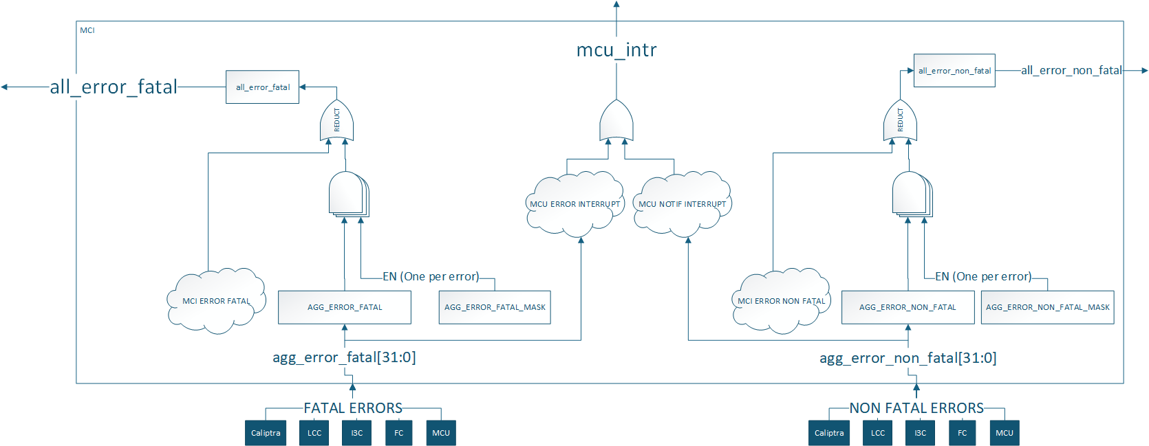
Aggregate error register assignments are documented in the register specification: TODO: Add a link to rdl -> html file
Regions of 6 bits in the aggregate error registers are reserved for each component. MCU and Caliptra errors are connected to appropriate severity levels. Lifecycle controller, fuse controller and I3C are connected to both severities. Masks are used to set the severity of each error for these components. These can be configured by integrators, ROM, or runtime firmware.
| Error Register Bits | Component | Default Error Severity | Description |
|---|---|---|---|
| Aggregate error[5:0] | Caliptra core | Both | Caliptra errors |
| Aggregate error[11:6] | MCU | Both | DCCM double bit ECC error is fatal DCCM single bit ECC error is non-fatal |
| Aggregate error[17:12] | Life cycle controller | Fatal | LCC alerts [14:12] |
| Aggregate error[23:18] | OTP Fuse controller | Fatal | FC Error [23], FC alerts [22:18] |
| Aggregate error[29:24] | I3C | Non-Fatal | Peripheral reset [25] and escalated reset [24] pins from I3C |
| Aggregate error[31:30] | Spare bits | None | Spare bits for integrator use |
MCI also generates error signals for its own internal blocks, specifically for MCU SRAM & mailboxes double bit ECC and WDT.
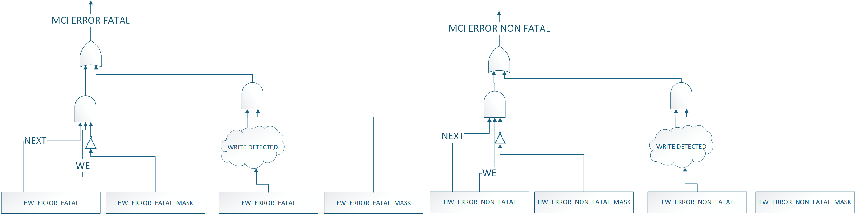
MCI Fuse Storage Support
MCI also provides capability to store fuses required for Caliptra subsystem for Caliptra core's usage for production debug unlock feature. MCU will read the fuse controller for the production debug unlock hashes , write to the corresponding registers in the MCI block and lock the registers from being changed by MCU RT FW. Lock is done by writing to do a FUSE_WR_DONE (FIXME: Add specific register & bit names).
MCU Timer
Standard RISC-V timer interrupts for MCU are implemented using the mtime and mtimecmp registers defined in the RISC-V Privileged Architecture Specification. Both mtime and mtimecmp are included in the MCI register bank, and are accessible by the MCU to facilitate precise timing tasks. Frequency for the timers is configured by the SoC using the dedicated timer configuration register, which satisfies the requirement prescribed in the RISC-V specification for such a mechanism. These timer registers drive the timer_int pin into the MCU.
MCU Trace Buffer
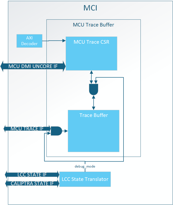
MCI hosts the MCU trace buffer. It can hold up to 64 trace packets from the MCU, see MCU Trace Buffer Packet for the data format. Read access to the trace buffer is controlled by the LCC state Translator. When Debug Locked all AXI and DMI accesses to the trace buffer are rejected. See MCU Trace Buffer Error Handling for expected response while Debug Locked.
MCU RISC-V processor can enable/disable tracing with an internal CSR, by default it is enabled. Within MCI there is no way to disable traces.
The trace buffer is a circular buffer where the oldest data is overwritten by new traces when the buffer is full. When a trace packet is stored the write pointer increments by MCU Trace Buffer Packet Size/DWORD
The trace buffer is reset when MCI reset is asserted (warm reset).
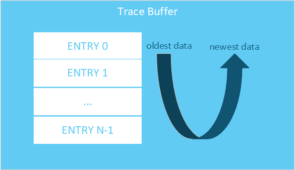
MCU Trace Buffer SW Interface
Below is the SW interface to extract trace data:
| Register Name | Access Type | Description |
|---|---|---|
| DATA | RO | Trace data at READ_PTR location |
| READ_PTR | RW | Read pointer in trace buffer for DATA. NOTE: this is not an address, meaning increment by 1 to get the next entry. |
| WRITE_PTR | RO | Offset to store next trace entry in trace buffer. If VALID_DATA is set, WRITE_PTR - 1 is the newest trace entry. |
| STATUS.VALID_DATA | RO | Indicates at least one entry is valid in the trace buffer. |
| STATUS.WRAPPED | RO | Indicates the trace buffer has wrapped at least once. Meaning all entries in the trace buffer are valid. If 0, then the oldest entry in the buffer is at ptr=0. If 1, the oldest entry is at WRITE_PTR |
| CONFIG.TRACE_BUFFER_DEPTH | RO | Indicates the total number of 32 bit entries in the trace buffer. TRACE_BUFFER_DEPTH - 1 is the last valid WRITE/READ_PTR entry in the trace buffer. NOTE: This is the trace buffer depth and not the number of MCU Trace Buffer Packets. |
MCU Trace Buffer Registers Spec
MCU Trace Buffer Packet
A single MCU trace packet is more than 32 bits, meaning each trace takes up more than one READ/WRITE_PTR entry. Trace data is stored in the following format:

Assuming there is only one trace stored in the trace buffer the WRITE_PTR would read as 0x4. To get the entire trace packet the user would need to read offsets 0x0, 0x1, 0x2, and 0x3.
MCU Trace Buffer Extraction
To extract trace buffer data the user should send the following transaction:
- Write READ_PTR
- Read DATA
Repeat these steps until all data required has been extracted.
The user should use the combination of WRITE_PTR, VALID_DATA, WRAPPED, and TRACE_BUFFER_DEPTH to know where valid data lives in the trace buffer.
MCU Trace Buffer Error Handling
AXI access to the MCU Trace Buffer while not in debug mode will result in an AXI error.
DMI access to the MCU Trace Buffer while not in debug mode will result in writes being dropped and reads returning 0.
If the user sets the READ_PTR > (TRACE_BUFFER_DEPTH - 1) and tries to read the DATA register, the behavior is undefined.
MCI Debug
MCI Debug Access
MCI provides DMI access via MCU TAP and a DEBUG AXI USER address for debug access to MCI.
MCI DMI
NOTE: DMI access to MBOX0/1 is not enabled in Caliptra 2.0. This will be enabled in future Caliptra versions
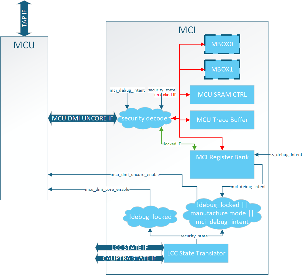
The DMI port on MCU is a dedicated interface that is controlled via the MCU TAP interface. MCI provides two services when it comes to DMI:
-
MCU DMI enable control (uncore and core)
-
DMI interface for debug access to MCI address space
MCU DMI Enable Control
The MCU has two different DMI enables:
- Core
- Access to internal MCU registers
- Uncore
- Access to MCI registers
MCI provides the logic for these enables. When the following condition(s) are met the enables are set:
MCU Core Enable: Debug Mode
MCU Uncore Enable: Debug Mode OR LCC Manufacturing Mode OR debug intent asserted (effective debug intent — physical strap OR SS_DEBUG_INTENT_MCU)
Note: These are the exact same controls Calipitra Core uses for DMI enable
MCI DMI Interface
The MCI DMI Interface gives select access to the blocks inside MCI.
Access to MCI's DMI space (MCU Uncore) is split into two different levels of security:
| Access | Description | | :--------- | :--------- | | Debug Locked| Registers and memories behind this security level are always accessible over DMI whenever MCU uncore DMI enabled.| | Debug Unlock| Registers and memories behind this security level are only accessible over DMI when LCC is Debug Unlocked.|
Illegal accesses will result in writes being dropped and reads returning 0.
NOTE: MCI DMI address space is different than MCI AXI address space.
MCI DMI Memory Map
| Register Name | DMI Address | Access Type | Debug Locked Access | Debug Unlock Access |
|---|---|---|---|---|
| NOT ENABLED IN 2.0 MBOX0_DLEN | 0x50 | RO | Yes | |
| NOT ENABLED IN 2.0 MBOX0_DOUT | 0x51 | RO | Yes | |
| NOT ENABLED IN 2.0 MBOX0_STATUS | 0x52 | RO | Yes | |
| NOT ENABLED IN 2.0 MBOX0_DIN | 0x53 | WO | Yes | |
| NOT ENABLED IN 2.0 MBOX1_DLEN | 0x54 | RO | Yes | |
| NOT ENABLED IN 2.0 MBOX1_DOUT | 0x55 | RO | Yes | |
| NOT ENABLED IN 2.0 MBOX1_STATUS | 0x56 | RO | Yes | |
| NOT ENABLED IN 2.0 MBOX1_DIN | 0x57 | WO | Yes | |
| MCU_SRAM_ADDR | 0x58 | RW | Yes | |
| MCU_SRAM_DATA | 0x59 | RW | Yes | |
| MCU_TRACE_STATUS | 0x5A | RO | Yes | |
| MCU_TRACE_CONFIG | 0x5B | RO | Yes | |
| MCU_TRACE_WR_PTR | 0x5C | RO | Yes | |
| MCU_TRACE_RD_PTR | 0x5D | RW | Yes | |
| MCU_TRACE_DATA | 0x5E | RO | Yes | |
| HW_FLOW_STATUS | 0x5F | RO | Yes | |
| RESET_REASON | 0x60 | RO | Yes | |
| RESET_STATUS | 0x61 | RO | Yes | |
| FW_FLOW_STATUS | 0x62 | RO | Yes | |
| HW_ERROR_FATAL | 0x63 | RO | Yes | |
| AGG_ERROR_FATAL | 0x64 | RO | Yes | |
| HW_ERROR_NON_FATAL | 0x65 | RO | Yes | |
| AGG_ERROR_NON_FATAL | 0x66 | RO | Yes | |
| FW_ERROR_FATAL | 0x67 | RO | Yes | |
| FW_ERROR_NON_FATAL | 0x68 | RO | Yes | |
| HW_ERROR_ENC | 0x69 | RO | Yes | |
| FW_ERROR_ENC | 0x6A | RO | Yes | |
| FW_EXTENDED_ERROR_INFO_0 | 0x6B | RO | Yes | |
| FW_EXTENDED_ERROR_INFO_1 | 0x6C | RO | Yes | |
| FW_EXTENDED_ERROR_INFO_2 | 0x6D | RO | Yes | |
| FW_EXTENDED_ERROR_INFO_3 | 0x6E | RO | Yes | |
| FW_EXTENDED_ERROR_INFO_4 | 0x6F | RO | Yes | |
| FW_EXTENDED_ERROR_INFO_5 | 0x70 | RO | Yes | |
| FW_EXTENDED_ERROR_INFO_6 | 0x71 | RO | Yes | |
| FW_EXTENDED_ERROR_INFO_7 | 0x72 | RO | Yes | |
| RESET_REQUEST | 0x73 | RW | Yes | |
| MCI_BOOTFSM_GO | 0x74 | RW | Yes | |
| CPTRA_BOOT_GO | 0x75 | RW | Yes | |
| FW_SRAM_EXEC_REGION_SIZE | 0x76 | RW | Yes | |
| MCU_RESET_VECTOR | 0x77 | RW | Yes | |
| SS_DEBUG_INTENT | 0x78 | RO | Yes | |
| SS_CONFIG_DONE | 0x79 | RW | Yes | |
| SS_CONFIG_DONE_STICKY | 0x7A | RW | Yes | |
| MCU_NMI_VECTOR | 0x7B | RW | Yes | |
| MCI_DMI_MCI_HW_OVERRIDE (DMI ONLY Reg) | 0x7C | RW | Yes |
DMI Only Registers
MCI_DMI_MCU_HW_OVERRIDE
| Field Name | Bits | Access Type | Description |
|---|---|---|---|
mcu_sram_fw_exec_region_lock | [0] | RW | mcu_sram_fw_exec_region_lock control. ORed with input signal giving debugger control if Caliptra Core in reset while attempting MCU reset flow. |
reserved | [31:1] | RW | Reserved |
DMI MCU SRAM Access
MCU SRAM is only accessable via DMI while in Debug Unlock. While in Debug Unlock DMI has RW permission to the entire MCU SRAM.
Due to limited DMI address space the MCU SRAM is accessable via a two register mailbox.
MCU_SRAM_ADDRMCU_SRAM_DATA
The first MCU SRAM address is at address 0x0. The address is byte addressable, but all accesses must be DWORD aligned. Failure to align the address will result in undefined behavior. Access to addresses beyond the MCU SRAM size will result in address wrapping.
To write content to the MCU SRAM the flow is:
- Write
MCU_SRAM_ADDR - Write
MCU_SRAM_DATA
To read content from the MCU SRAM the flow is:
- Write
MCU_SRAM_ADDR - Read
MCU_SRAM_DATA
There is no error response on the DMI port, so any ECC error must be checked via the ECC registers in the MCI Register Bank.
Important: MCU core must be halted to access MCU SRAM via DMI. Failure to do so will result in collisions between the two interfaces and an error will be reported.
DMI MCU Trace Buffer Access
Access to the MCU Trace buffer via DMI is the same SW interface as specified in MCU Trace Buffer.
Access is limited to Debug Unlock mode only. Access to this space while not in Debug Unlock will result in writes being dropped and reads return 0x0.
MCI Boot FSM Breakpoint
The MCI Breakpoint is used as a stopping point for debugging Caliptra SS. At this breakpoint the user can either use one of the MCI Debug Access mechanisms to configure MCI before bringing MCU or Caliptra out of reset.
MCI Boot FSM Breakpoint Flow
- Assert mci_boot_seq_brkpoint
- Deassert MCI Reset
- DEBUG ACCESS TO MCI
- Set MCI's BRKPOINT_GO register to 1
- Through one of the MCI Debug Access methods.
- FSM will continue
MCI Design for Test (DFT)
Reset Controls
MCI controls various resets for other IPs like MCU and Caliptra Core. When the scan_mode input port is set these resets are directly controlled by the mcu_rst_b input intead of the internal MCI logic.
84daa9a
Caliptra Subsystem Integration Specification
Version 2p1
- Scope
- Overview
- Caliptra Subsystem High level diagram
- Integration Considerations
- Verification View of Caliptra Subsystem
- Caliptra Subsystem Top
- Caliptra Core
- MCU (Manufacturer Control Unit)
- Fuse Controller
- Overview
- Parameters & Defines
- Interface
- Fuse Macro Memory Map and Fuse Controller CSR Address Map
- FC Integration Requirements
- Direct Access Interface
- Initialization
- Programming interface
- Readout Sequence
- Sequences: Reset, Boot
- UDS & Field Entropy FIPS Zeroization Sequence
- FIPS Zeroization Sequence For ECC
- Miscellanious Fuse Integration Guidelines
- How to test : Smoke & more
- Generating the Fuse Partitions
- Fuse Controller Macro
- Life Cycle Controller
- MCI
- Overview
- Parameters & Defines
- Interface
- Memory Map / Address map
- MCI Integration Requirements
- Error Aggregation Connectivity Requirements
- Subsystem Internal Fuse Controller Initialization Connectivity Requirements
- Subsystem Internal Life Cycle Controller Initialization Connectivity Requirements
- MCI MCU Connectivity Requirements
- MCI Caliptra Core Connectivity Requirements
- LCC Gasket Connectivity Requirements
- MCU SRAM Sizing Requirements
- MCU MBOX SRAM Sizing Requirements
- Programming interface
- Sequences : Reset, Boot,
- Other requirements
- I3C core
- CDC analysis and constraints
- Reset Domain Crossing
- Synthesis
- Terminology
Scope
For Caliptra Subsystem, this document serves as a hardware integration specification. The scope of this document is to assist integrators in the integration of Caliptra Subsystem. It is not intended to serve as a hardware specification or to include micro-architectural details. This document includes Caliptra Subsystem top-level details along with parameters, defines, interfaces, memory map, programming reference, and guidelines on how to test the integration of the design.
Document Version
| Date | Document Version | Description |
|---|---|---|
| Jan 31st, 2025 | v0p8 | Work in progress |
| Apr 30th, 2025 | v1p0-rc1 | Initial release candidate of Caliptra Gen 2.0 Subsystem Documents. Specifcations updated with: - Detail on usage of all Subsystem flows such as Streaming Boot, Mailbox operation, and Debug Unlock - Details on design connectivity with top-level ports - Requirements and recommendations for integrators when adding Caliptra Subsystem to SoC designs |
| Oct 12th, 2025 | v2p1 | Final release of Caliptra Subsystem 2.1 |
Related repositories & specifications
The components described in this document are either obtained from open-source GitHub repositories, developed from scratch, or modified versions of open-source implementations. Links to relevant documentation and GitHub sources are shared in the following table.
Table 1: Related specification and repositories
| IP/Block | Code (GitHub URL) | Documentation (URL) |
|---|
| Caliptra | GitHub - chipsalliance/Caliptra| Caliptra Gen 2.0 Specification | Caliptra-SS | GitHub - chipsalliance/caliptra-ss| Hardware Specification Document | Caliptra-rtl | GitHub - chipsalliance/caliptra-rtl | Caliptra RTL documentation | | Cores-VeeR | GitHub - chipsalliance/Cores-VeeR-EL2 | VeeR EL2 Programmer’s Reference Manual | | I3C-Core | GitHub - chipsalliance/i3c-core | I3C core documentation | | Adams Bridge | GitHub - chipsalliance/adams-bridge | Adams Bridge Documentation |
Overview
The Caliptra Subsystem is designed to provide a robust Root of Trust (RoT) for datacenter-class System on Chips (SoCs), including CPUs, GPUs, DPUs, and TPUs. It integrates both hardware and firmware components to deliver essential security services such as identity establishment, measured boot, and attestation. By incorporating the Caliptra Subsystem, integrators can enhance the security capabilities of their SoCs, providing a reliable RoT that meets industry standards and addresses the evolving security needs of datacenter environments.
Caliptra Subsystem High level diagram
The following diagram provides a high-level overview of the Caliptra subsystem. It illustrates the key components and their interconnections within the system. For an in-depth understanding of the Caliptra Subystem refer to Caliptra Subsystem Hardware Specification Document.
Following high-level diagram helps integrators understand the overall architecture and the relationships between different components within the Caliptra subsystem.
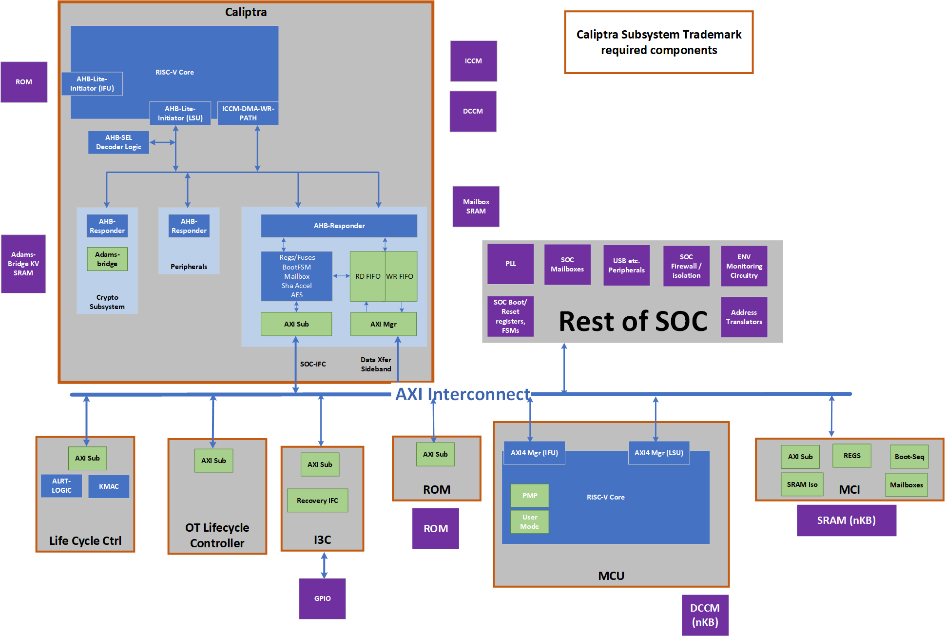
Caliptra Subsystem includes:
- Caliptra Core: The Caliptra Core IP. For more information, see Caliptra: A Datacenter System on a Chip (SoC) Root of Trust (RoT).
- MCU (Manufacturer Control Unit): A microcontroller unit that manages various control tasks within the subsystem.
- I3C Core: An interface for connecting and communicating with I3C devices, which are used for providing streaming boot support and communicating with other I3C host controllers.
- Life Cycle Controller: A component that manages the different stages of the subsystem's lifecycle, including initialization, operation, and shutdown.
- Fuse Controller (OTP): A one-time programmable memory controller used for storing critical configuration data and security keys.
- MCI (Manufacturer Control Interface (for MCU)): Manages the communication between the processor and the memory components.
- Memories: Various memory components used for storing data and instructions required by the subsystem.
Integration Considerations
By performing these design and verification tasks, the integrator ensures that the Caliptra Subsystem is properly integrated and can function as intended within the larger system. Several files contain code that may be specific to an integrator's implementation and should be overridden. This overridable code is either configuration parameters with integrator-specific values or modules that implement process-specific functionality. Code in these files should be modified or replaced by integrators using components from the cell library of their fabrication vendor. The following table describes recommended modifications for each file.
| File | Description |
|---|---|
| css_mcu0_dmi_jtag_to_core_sync.v | Replace with a technology-specific sync cell. This synchronizer implements edge detection logic using a delayed flip flop on the output domain to produce a pulse output. Integrators must take care to ensure logical equivalence when replacing this logic with custom cells. |
| css_mcu0_beh_lib.sv | Replace css_mcu0_rvclkhdr/css_mcu0_rvoclkhdr with a technology-specific clock gater. Modifying this file may not be necessary if integrators override the clock gate module that is used by setting TECH_SPECIFIC_EC_RV_ICG. |
| css_mcu0_beh_lib.sv | Replace css_mcu0_rvsyncss (and css_mcu0_rvsyncss_fpga if the design will be implemented on an FPGA) with a technology-specific sync cell. |
| src/integration/rtl/caliptra_ss_includes.svh | Modify the parameter CPTRA_SS_ROM_SIZE_KB to define the correct size of the MCU ROM in integrated design. No other parameters in this file are permitted to be modified. |
Caliptra Core RTL modifications
It is mandatory that any build processes used (e.g. simulation, lint, synthesis) define the Verilog macro CALIPTRA_MODE_SUBSYSTEM, as described in the Caliptra Core Integration Specification. This ensures that Caliptra provides all Subsystem-related features and configuration. Example build scripts provided in the Caliptra Subsystem repository (such as Makefile) demonstrate how this might be performed.
Design Considerations
- Replace the AXI Interconnect: The subsystem utilizes an AXI-based interconnect to facilitate communication between components, with the Caliptra core connecting via an AXI interface. The integrator must replace the default AXI interconnect component with their proprietary interface. This ensures that the subsystem can communicate effectively with the rest of the subsystem components using the integrator's specific interconnect architecture.
- Connect the Memories: The integrator must connect the various memory components required by the subsystem. These memory components are used for storing data and instructions necessary for the operation of the Caliptra subsystem.
- No Changes to Internals: Integrators are not expected to make any changes to the internals of the design. The focus should be on ensuring proper integration and connectivity of the subsystem components.
Verification Considerations
- Connect the I3C Core GPIO with I3C host driver: The integrator must connect the I3C core (two target I3C devices) to the appropriate driver for the GPIO pins. This connection is crucial for enabling communication with I3C devices, which are used for communication within the subsystem.
Verification View of Caliptra Subsystem
The following block diagram shows details on verification view of Caliptra Subsystem
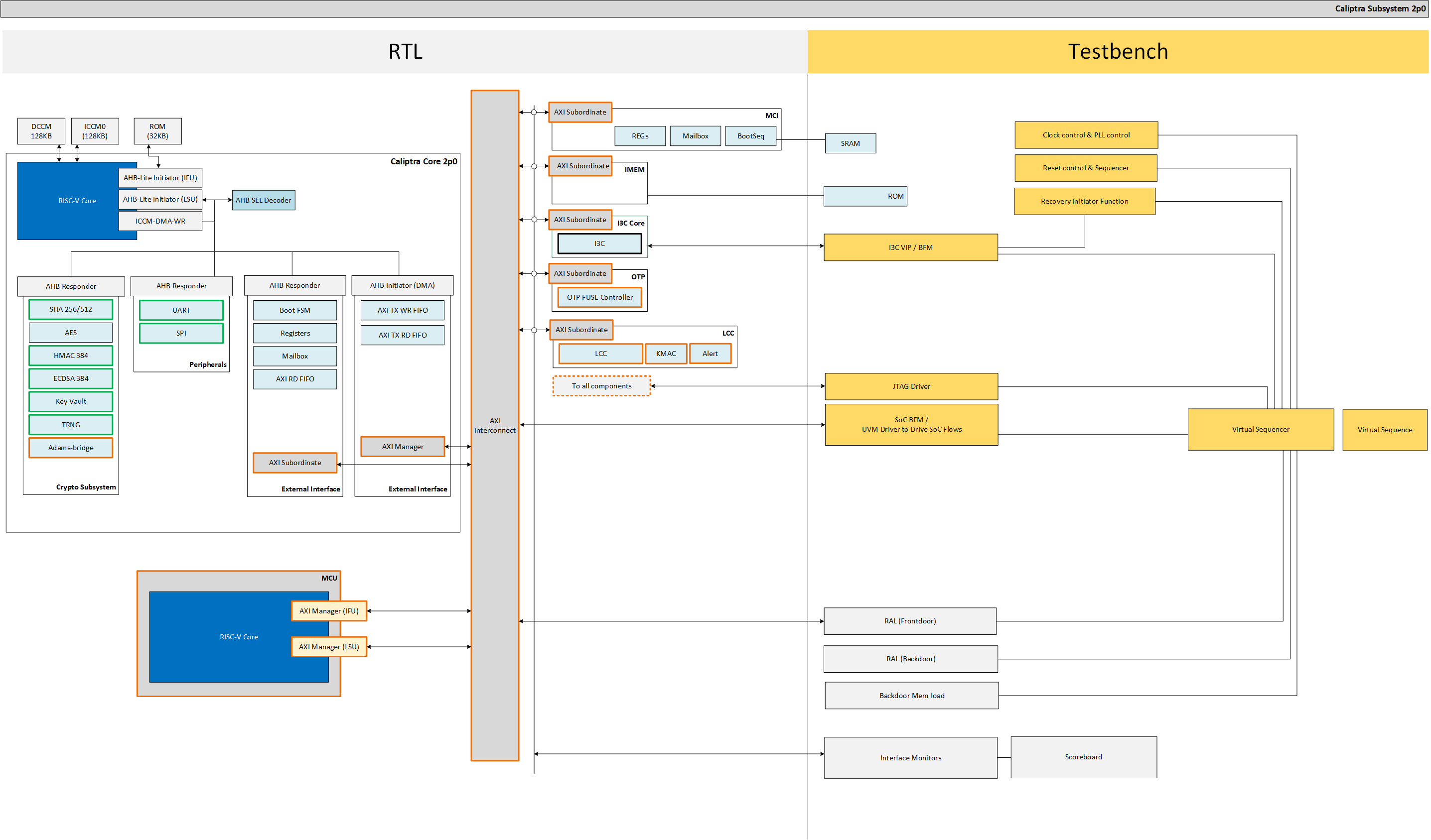
Memory Requirements
Integrators must instantiate SRAM components outside of the Caliptra Subsystem boundary (see SRAM Implementation for more details). SRAM wrapper logic within the Caliptra Subsystem boundary facilitates the connection to SRAM instances through memory export interfaces in the top-level port list. Integrators must connect the following memory export interfaces to the instantiated SRAM components.
SoC Specific in below table means the size of the memory is not fixed and can be configured based on the design requirements by integrator. The actual size will depend on the specific implementation and configuration of the Caliptra Subsystem.
| Device | Memory Name | Interface | Size | Access Type | Description |
|---|---|---|---|---|---|
| MCU0 | Instruction ROM | mcu_rom_mem_export_if | SoC Specific | Read-Only | Stores the instructions for MCU0 execution. Write-enable (we) and write-data (wdata) signals must be left unconnected, as MCU ROM has no write support. |
| MCU0 | Memory Export | cptra_ss_mcu0_el2_mem_export | SoC Specific | Read/Write | Memory export for MCU0 access. |
| MCU0 | Shared Memory (SRAM) | cptra_ss_mci_mcu_sram_req_if | SoC Specific | Read/Write | Shared memory between MCI and MCU for data storage. |
| MAILBOX | MBOX0 Memory | cptra_ss_mci_mbox0_sram_req_if | SoC Specific | Read/Write | Memory for MBOX0 communication. |
| MAILBOX | MBOX1 Memory | cptra_ss_mci_mbox1_sram_req_if | SoC Specific | Read/Write | Memory for MBOX1 communication. |
| Caliptra Core | ICCM, DCCM | cptra_ss_cptra_core_el2_mem_export | Refer to Caliptra Core Integration Specification | Read/Write | Interface for the Instruction and Data Closely Coupled Memory (ICCM, DCCM) of the core. |
| Caliptra Core | Caliptra ROM | cptra_ss_cptra_core_imem | Refer to Caliptra Core Integration Specification | Read-Only | Interface for Caliptra ROM. |
| Caliptra Core | Caliptra Mailbox SRAM | cptra_ss_cptra_core_mbox_sram | Refer to Caliptra Core Integration Specification | Read/Write | Interface for Caliptra mailbox memory. |
| Caliptra Core | Adams Bridge SRAM | abr_memory_export_req | Refer to Adams Bridge Documentation | Read/Write | Interface for SRAM instantiated within Adams Bridge block. |
Caliptra Subsystem Top
The integration of the Caliptra Subsystem begins with the instantiation of the top-level RTL module, caliptra_ss_top.sv. This module serves as the primary entry point for the subsystem and encapsulates all the logic and components required for the functionality of the Caliptra Root of Trust (RoT). All signals must be connected based on the detailed interface and signal descriptions provided in this document. Ensure adherence to the signal direction, width, and functionality to guarantee proper integration with the host SoC.
Parameters & Defines
File at this path in the repository includes parameters and defines for Caliptra Subsystem src/integration/rtl/caliptra_ss_includes.svh
Interfaces & Signals
IMPORTANT NOTE: All signals assumed to by synchronous to cptra_ss_clk_i.
Table: Caliptra SS Straps
| Facing | Type | width | Name | Description |
|---|---|---|---|---|
| External | input | 32 | cptra_ss_strap_mcu_lsu_axi_user_i | MCU LSU AXI user strap input |
| External | input | 32 | cptra_ss_strap_mcu_ifu_axi_user_i | MCU IFU AXI user strap input |
| External | input | 32 | cptra_ss_strap_mcu_sram_config_axi_user_i | MCU SRAM Configuration AXI user strap input. |
| External | input | 32 | cptra_ss_strap_mci_soc_config_axi_user_i | MCI SOC Configuration AXI user strap input |
| External | input | 32 | cptra_ss_strap_caliptra_dma_axi_user_i | Caliptra DMA AXI user strap input |
| External | input | 32 | cptra_ss_strap_mcu_reset_vector_i | MCU reset vector strap input |
| External | input | 64 | cptra_ss_strap_caliptra_base_addr_i | Caliptra base address strap input |
| External | input | 64 | cptra_ss_strap_mci_base_addr_i | MCI base address strap input |
| External | input | 64 | cptra_ss_strap_recovery_ifc_base_addr_i | Recovery interface base address strap input |
| External | input | 64 | cptra_ss_strap_external_staging_area_base_addr_i | External staging area base address input |
| External | input | 64 | cptra_ss_strap_otp_fc_base_addr_i | OTP FC base address strap input |
| External | input | 64 | cptra_ss_strap_uds_seed_base_addr_i | UDS seed base address strap input |
| External | input | 32 | cptra_ss_strap_prod_debug_unlock_auth_pk_hash_reg_bank_offset_i | Prod debug unlock auth PK hash reg bank offset input |
| External | input | 32 | cptra_ss_strap_num_of_prod_debug_unlock_auth_pk_hashes_i | Number of prod debug unlock auth PK hashes input |
| External | input | 32 | cptra_ss_strap_generic_0_i | Provides the Caliptra ROM with a 32-bit pointer that encodes the location of the fuse controller's status register and the bit position of the idle indicator. Upper 16 bits: Bit index of the IDLE_BIT_STATUS within SOC_OTP_CTRL_STATUS. Lower 16 bits: Offset address of SOC_OTP_CTRL_STATUS within the SOC_IFC_REG space, relative to SOC_OTP_CTRL_BASE_ADDR. |
| External | input | 32 | cptra_ss_strap_generic_1_i | Provides the Caliptra ROM with a 32-bit pointer to the fuse controller’s command register (CMD), enabling ROM-level control or triggering of fuse operations. |
| External | input | 32 | cptra_ss_strap_generic_2_i | Generic strap input 2 |
| External | input | 32 | cptra_ss_strap_generic_3_i | Generic strap input 3 |
| External | input | 1 | cptra_ss_debug_intent_i | Physical presence bit required to initiate the debug unlock flow. For more details, refer to the Production Debug Unlock Flow and How does Caliptra Subsystem enable manufacturing debug mode?. For SOCs that choose to use these features, this port should be connected to a GPIO |
| External | input | 16 | cptra_ss_strap_key_release_key_size_i | OCP L.O.C.K. MEK byte size. Expected to be 0x40. |
| External | input | 64 | cptra_ss_strap_key_release_base_addr_i | OCP L.O.C.K. MEK release base address. |
| External | input | 1 | cptra_ss_strap_ocp_lock_en_i | OCP L.O.C.K. enable. Allows OCP L.O.C.K. in progress to be set enabling hardware features specific to OCP L.O.C.K. such as AES Keyvault write path, Keyvault filtering rules, and Key Release via AXI DMA. Must be driven with a constant value 0 or 1. |
| External | input | 64 | cptra_ss_strap_external_staging_area_base_addr_i | Base AXI address for the external staging area used by Caliptra Core FW to stage FW images due to reduced MBOX SRAM size. See Caliptra External Staging Area for more details. |
Strap Timing Requirements
All strap inputs listed in the table above, as well as cptra_ss_cptra_obf_key_i, cptra_ss_cptra_csr_hmac_key_i, cptra_ss_lc_sec_volatile_raw_unlock_en_i, cptra_ss_lc_Allow_RMA_or_SCRAP_on_PPD_i, and cptra_ss_FIPS_ZEROIZATION_PPD_i, must be driven to their intended values and held stable before cptra_ss_rst_b_i is deasserted. These signals must not transition for the duration of the boot session (until the next reset assertion).
Internally, strap values are consumed at different points during the boot sequence, all of which occur strictly after cptra_ss_rst_b_i deasserts. The internal sampling cascade is:
| Order | Internal Event | Straps Consumed |
|---|---|---|
| 1 | MCI boot sequencer starts (on cptra_ss_rst_b_i deassertion) | cptra_ss_lc_sec_volatile_raw_unlock_en_i, cptra_ss_lc_Allow_RMA_or_SCRAP_on_PPD_i (used combinationally in LC controller FSM during init) |
| 2 | MCI boot sequencer deasserts internal SS reset (cptra_ss_rst_b_o) during BOOT_OTP_FC state | MCI register straps latched on a 1-cycle write-enable pulse: cptra_ss_strap_mcu_reset_vector_i, cptra_ss_strap_mcu_lsu_axi_user_i (registered copy), cptra_ss_strap_mcu_ifu_axi_user_i (registered copy), cptra_ss_strap_mcu_sram_config_axi_user_i, cptra_ss_strap_mci_soc_config_axi_user_i, cptra_ss_debug_intent_i, cptra_ss_FIPS_ZEROIZATION_PPD_i |
| 3 | MCI boot sequencer deasserts Caliptra core reset (cptra_ss_mci_cptra_rst_b_o) during BOOT_CPTRA state | cptra_ss_cptra_obf_key_i (latched into internal register), cptra_ss_cptra_csr_hmac_key_i (latched on cptra_noncore_rst_b deassertion, only in DEVICE_MANUFACTURING lifecycle) |
| 4 | Caliptra internal boot FSM deasserts cptra_noncore_rst_b during BOOT_FUSE state | Caliptra soc_ifc register straps latched on a 1-cycle write-enable pulse (locked after fuse_done): cptra_ss_strap_caliptra_base_addr_i, cptra_ss_strap_mci_base_addr_i, cptra_ss_strap_recovery_ifc_base_addr_i, cptra_ss_strap_otp_fc_base_addr_i, cptra_ss_strap_uds_seed_base_addr_i, cptra_ss_strap_caliptra_dma_axi_user_i, cptra_ss_strap_generic_0_i through cptra_ss_strap_generic_3_i, cptra_ss_strap_prod_debug_unlock_auth_pk_hash_reg_bank_offset_i, cptra_ss_strap_num_of_prod_debug_unlock_auth_pk_hashes_i, cptra_ss_strap_key_release_key_size_i, cptra_ss_strap_key_release_base_addr_i, cptra_ss_strap_ocp_lock_en_i, cptra_ss_strap_external_staging_area_base_addr_i |
Security note — unregistered AXI identity straps:
cptra_ss_strap_mcu_lsu_axi_user_iandcptra_ss_strap_mcu_ifu_axi_user_iare wired directly (combinationally) to the MCU AXI busaruser/awuserfields in addition to being captured into MCI registers. The combinational path means these signals are security-critical at all times — not just at the sampling edge. Toggling them during operation would corrupt in-flight AXI transactions and could bypass fuse controller access control checks that rely on AXI user identity. SoC integrators must ensure these are driven from a constant source (e.g., tied to fixed logic values or hard-strapped).
AXI Interface (axi_if)
| Signal | Width | Direction (mgr) | Direction (sub) |
|---|---|---|---|
araddr | AW | output | input |
arburst | $bits(axi_burst_e) | output | input |
arsize | 3 | output | input |
arlen | 8 | output | input |
aruser | UW | output | input |
arid | IW | output | input |
arlock | 1 | output | input |
arvalid | 1 | output | input |
arready | 1 | input | output |
rdata | DW | input | output |
rresp | $bits(axi_resp_e) | input | output |
rid | IW | input | output |
rlast | 1 | input | output |
rvalid | 1 | input | output |
rready | 1 | output | input |
awaddr | AW | output | input |
awburst | $bits(axi_burst_e) | output | input |
awsize | 3 | output | input |
awlen | 8 | output | input |
awuser | UW | output | input |
awid | IW | output | input |
awlock | 1 | output | input |
awvalid | 1 | output | input |
awready | 1 | input | output |
wdata | DW | output | input |
wstrb | DW/8 | output | input |
wvalid | 1 | output | input |
wready | 1 | input | output |
wlast | 1 | output | input |
bresp | $bits(axi_resp_e) | input | output |
bid | IW | input | output |
bvalid | 1 | input | output |
bready | 1 | output | input |
Caliptra Subsystem Top Interface & Signals
| Facing | Type | width | Signal or Interface Name | Description |
|---|---|---|---|---|
| External | input | 1 | cptra_ss_clk_i | Caliptra subsystem clock input |
| External | input | 1 | cptra_ss_pwrgood_i | Power good signal input |
| External | input | 1 | cptra_ss_rst_b_i | Reset signal input, active low |
| External | input | 1 | cptra_ss_mci_cptra_rst_b_i | Reset signal input for Caliptra Core, active low. See Caliptra Core Reset Control for more details |
| External | output | 1 | cptra_ss_mci_cptra_rst_b_o | Reset signal output from MCI for Caliptra Core, active low. See Caliptra Core Reset Control for more details |
| External | input | 1 | cptra_ss_mcu_rst_b_i | Reset signal input for MCU, active low. See MCU Reset Control for more details |
| External | output | 1 | cptra_ss_mcu_rst_b_o | Reset signal output for MCU, active low. See MCU Reset Control for more details |
| External | output | 1 | cptra_ss_warm_reset_rdc_clk_dis_o | Clock disable for warm reset. Used to disable cptra_ss_rdc_clk_cg_o and cptra_ss_mcu_clk_cg_o clocks. Asserted a few clock cycles after cptra_ss_rst_b_i asserted and before cptra_ss_rst_b_o asserted. Deasserted a few clock cycles after cptra_ss_rst_b_i deasserted. |
| External | output | 1 | cptra_ss_early_warm_reset_warn_o | Early reset warn used to change security related signals to a safe value before reset is asserted. Needed since Caliptra Core clock gating is slightly after MCI clock gating/reset assertion. Example is the security_state fed from MCI to Caliptra Core. |
| External | output | 1 | cptra_ss_mcu_fw_update_rdc_clk_dis_o | Clock disable for MCU reset. Used to disable cptra_ss_mcu_clk_cg_o clock. Asserted a few clock cycles before cptra_ss_mcu_rst_b_o is asserted. Deasserted when MCI boot sequencer switches out of BOOT_RST_MCU state. |
| External | output | 1 | cptra_ss_rdc_clk_cg_o | Caliptra subsystem clock gated clock for RDC. Clock Control |
| External | output | 1 | cptra_ss_mcu_clk_cg_o | MCU clock gated clock for RDC. Clock Control |
| External | output | 1 | cptra_ss_rst_b_o | Caliptra subsystem reset aligned for RDC crossing Reset Control |
| External | axi_if | na | cptra_ss_cptra_core_s_axi_if_w_sub | Caliptra core AXI write sub-interface |
| External | axi_if | na | cptra_ss_cptra_core_s_axi_if_r_sub | Caliptra core AXI read sub-interface |
| External | axi_if | na | cptra_ss_cptra_core_m_axi_if_w_mgr | Caliptra core AXI write manager interface |
| External | axi_if | na | cptra_ss_cptra_core_m_axi_if_r_mgr | Caliptra core AXI read manager interface |
| External | axi_if | na | cptra_ss_mci_s_axi_if_w_sub | Caliptra Subsystem MCI AXI write sub-interface |
| External | axi_if | na | cptra_ss_mci_s_axi_if_r_sub | Caliptra Subsystem MCI AXI read sub-interface |
| External | axi_if | na | cptra_ss_mcu_rom_s_axi_if_w_sub | Caliptra Subsystem MCU ROM AXI write sub-interface. Writes to MCU ROM are not supported, this interface shall be left unconnected from AXI interconnect and tied to 0-value inputs. |
| External | axi_if | na | cptra_ss_mcu_rom_s_axi_if_r_sub | Caliptra Subsystem MCU ROM AXI read sub-interface |
| External | axi_if | na | cptra_ss_mcu_lsu_m_axi_if_w_mgr | Caliptra Subsystem MCU LSU AXI write manager interface |
| External | Output | 4 | cptra_ss_mcu_lsu_m_axi_if_awcache | Caliptra Subsystem MCU LSU AXI write manager address transaction attributes signal |
| External | Output | 3 | cptra_ss_mcu_lsu_m_axi_if_awprot | Caliptra Subsystem MCU LSU AXI write manager address protection type signal |
| External | Output | 4 | cptra_ss_mcu_lsu_m_axi_if_awregion | Caliptra Subsystem MCU LSU AXI write manager address region identifier signal |
| External | Output | 4 | cptra_ss_mcu_lsu_m_axi_if_awqos | Caliptra Subsystem MCU LSU AXI write manager address quality of service signal |
| External | axi_if | na | cptra_ss_mcu_lsu_m_axi_if_r_mgr | Caliptra Subsystem MCU LSU AXI read manager interface |
| External | Output | 4 | cptra_ss_mcu_lsu_m_axi_if_arcache | Caliptra Subsystem MCU LSU AXI read manager address transaction attributes signal |
| External | Output | 3 | cptra_ss_mcu_lsu_m_axi_if_arprot | Caliptra Subsystem MCU LSU AXI read manager address protection type signal |
| External | Output | 4 | cptra_ss_mcu_lsu_m_axi_if_arregion | Caliptra Subsystem MCU LSU AXI read manager address region identifier signal |
| External | Output | 4 | cptra_ss_mcu_lsu_m_axi_if_arqos | Caliptra Subsystem MCU LSU AXI read manager address quality of service signal |
| External | axi_if | na | cptra_ss_mcu_ifu_m_axi_if_w_mgr | Caliptra Subsystem MCU IFU AXI write manager interface |
| External | Output | 4 | cptra_ss_mcu_ifu_m_axi_if_awcache | Caliptra Subsystem MCU IFU AXI write manager address transaction attributes signal |
| External | Output | 3 | cptra_ss_mcu_ifu_m_axi_if_awprot | Caliptra Subsystem MCU IFU AXI write manager address protection type signal |
| External | Output | 4 | cptra_ss_mcu_ifu_m_axi_if_awregion | Caliptra Subsystem MCU IFU AXI write manager address region identifier signal |
| External | Output | 4 | cptra_ss_mcu_ifu_m_axi_if_awqos | Caliptra Subsystem MCU IFU AXI write manager address quality of service signal |
| External | axi_if | na | cptra_ss_mcu_ifu_m_axi_if_r_mgr | Caliptra Subsystem MCU IFU AXI read manager interface |
| External | Output | 4 | cptra_ss_mcu_ifu_m_axi_if_arcache | Caliptra Subsystem MCU IFU AXI read manager address transaction attributes signal |
| External | Output | 3 | cptra_ss_mcu_ifu_m_axi_if_arprot | Caliptra Subsystem MCU IFU AXI read manager address protection type signal |
| External | Output | 4 | cptra_ss_mcu_ifu_m_axi_if_arregion | Caliptra Subsystem MCU IFU AXI read manager address region identifier signal |
| External | Output | 4 | cptra_ss_mcu_ifu_m_axi_if_arqos | Caliptra Subsystem MCU IFU AXI read manager address quality of service signal |
| External | axi_if | na | cptra_ss_mcu_sb_m_axi_if_w_mgr | Caliptra Subsystem MCU System Bus AXI write manager interface |
| External | Output | 4 | cptra_ss_mcu_sb_m_axi_if_awcache | Caliptra Subsystem MCU System Bus AXI write manager address transaction attributes signal |
| External | Output | 3 | cptra_ss_mcu_sb_m_axi_if_awprot | Caliptra Subsystem MCU System Bus AXI write manager address protection type signal |
| External | Output | 4 | cptra_ss_mcu_sb_m_axi_if_awregion | Caliptra Subsystem MCU System Bus AXI write manager address region identifier signal |
| External | Output | 4 | cptra_ss_mcu_sb_m_axi_if_awqos | Caliptra Subsystem MCU System Bus AXI write manager address quality of service signal |
| External | axi_if | na | cptra_ss_mcu_sb_m_axi_if_r_mgr | Caliptra Subsystem MCU System Bus AXI read manager interface |
| External | Output | 4 | cptra_ss_mcu_sb_m_axi_if_arcache | Caliptra Subsystem MCU System Bus AXI read manager address transaction attributes signal |
| External | Output | 3 | cptra_ss_mcu_sb_m_axi_if_arprot | Caliptra Subsystem MCU System Bus AXI read manager address protection type signal |
| External | Output | 4 | cptra_ss_mcu_sb_m_axi_if_arregion | Caliptra Subsystem MCU System Bus AXI read manager address region identifier signal |
| External | Output | 4 | cptra_ss_mcu_sb_m_axi_if_arqos | Caliptra Subsystem MCU System Bus AXI read manager address quality of service signal |
| External | axi_if | na | cptra_ss_i3c_s_axi_if_w_sub | Caliptra Subsystem I3C AXI write sub-interface |
| External | axi_if | na | cptra_ss_i3c_s_axi_if_r_sub | Caliptra Subsystem I3C AXI read sub-interface |
| External | input | na | cptra_ss_lc_axi_wr_req_i | LC controller AXI write request input |
| External | output | na | cptra_ss_lc_axi_wr_rsp_o | LC controller AXI write response output |
| External | input | na | cptra_ss_lc_axi_rd_req_i | LC controller AXI read request input |
| External | output | na | cptra_ss_lc_axi_rd_rsp_o | LC controller AXI read response output |
| External | input | 128 | cptra_ss_raw_unlock_token_hashed_i | Hashed token for RAW unlock |
| External | input | na | cptra_ss_otp_core_axi_wr_req_i | OTP controller AXI write request input |
| External | output | na | cptra_ss_otp_core_axi_wr_rsp_o | OTP controller AXI write response output |
| External | input | na | cptra_ss_otp_core_axi_rd_req_i | OTP controller AXI read request input |
| External | output | na | cptra_ss_otp_core_axi_rd_rsp_o | OTP controller AXI read response output |
| External | input | 256 | cptra_ss_cptra_obf_key_i | Caliptra core obfuscation key input |
| External | input | CLP_CSR_HMAC_KEY_DWORDS | cptra_ss_cptra_csr_hmac_key_i | Caliptra core CSR HMAC key input |
| External | input | 1 | cptra_ss_cptra_core_jtag_tck_i | JTAG clock input |
| External | input | 1 | cptra_ss_cptra_core_jtag_tms_i | JTAG TMS input |
| External | input | 1 | cptra_ss_cptra_core_jtag_tdi_i | JTAG TDI input |
| External | input | 1 | cptra_ss_cptra_core_jtag_trst_n_i | JTAG reset input, active low |
| External | output | 1 | cptra_ss_cptra_core_jtag_tdo_o | JTAG TDO output |
| External | output | 1 | cptra_ss_cptra_core_jtag_tdoEn_o | JTAG TDO enable output |
| External | output | 125 | cptra_ss_cptra_generic_fw_exec_ctrl_o | Generic firmware execution control output |
| External | output | 1 | cptra_ss_cptra_generic_fw_exec_ctrl_2_mcu_o | Generic firmware execution control bit 2 from Caliptra output |
| External | input | 1 | cptra_ss_cptra_generic_fw_exec_ctrl_2_mcu_i | Generic firmware execution control bit 2 for MCU input |
| External | output | 1 | cptra_ss_all_error_fatal_o | Caliptra SS fatal error |
| External | output | 1 | cptra_ss_all_error_non_fatal_o | Caliptra SS non-fatal error |
| External | input | na | cptra_ss_lc_ctrl_jtag_i | LC controller JTAG request input |
| External | output | na | cptra_ss_lc_ctrl_jtag_o | LC controller JTAG response output |
| External | interface | na | cptra_ss_cptra_core_el2_mem_export | Caliptra core EL2 memory export interface |
| External | interface | na | mcu_rom_mem_export_if | MCU ROM memory export interface. Write-enable (we) and write-data (wdata) signals must be left unconnected, as MCU ROM has no write support. |
| External | output | 1 | cptra_ss_cptra_core_mbox_sram_cs_o | Mailbox SRAM chip select output |
| External | output | 1 | cptra_ss_cptra_core_mbox_sram_we_o | Mailbox SRAM write enable output |
| External | output | CPTRA_MBOX_ADDR_W | cptra_ss_cptra_core_mbox_sram_addr_o | Mailbox SRAM address output |
| External | output | CPTRA_MBOX_DATA_AND_ECC_W | cptra_ss_cptra_core_mbox_sram_wdata_o | Mailbox SRAM write data output |
| External | input | CPTRA_MBOX_DATA_AND_ECC_W | cptra_ss_cptra_core_mbox_sram_rdata_i | Mailbox SRAM read data input |
| External | output | 1 | cptra_ss_cptra_core_imem_cs_o | Instruction memory chip select output |
| External | output | CALIPTRA_IMEM_ADDR_WIDTH | cptra_ss_cptra_core_imem_addr_o | Instruction memory address output |
| External | input | CALIPTRA_IMEM_DATA_WIDTH | cptra_ss_cptra_core_imem_rdata_i | Instruction memory read data input |
| External | input | 1 | cptra_ss_cptra_core_bootfsm_bp_i | Boot FSM breakpoint input |
| External | output | 1 | cptra_ss_cptra_core_etrng_req_o | External TRNG request output |
| External | input | 4 | cptra_ss_cptra_core_itrng_data_i | Internal TRNG data input |
| External | input | 1 | cptra_ss_cptra_core_itrng_valid_i | Internal TRNG valid input |
| External | interface | na | cptra_ss_mci_mcu_sram_req_if | MCI MCU SRAM request interface |
| External | interface | na | cptra_ss_mci_mbox0_sram_req_if | MCI mailbox 0 SRAM request interface |
| External | interface | na | cptra_ss_mci_mbox1_sram_req_if | MCI mailbox 1 SRAM request interface |har
| External | output | 1 | cptra_ss_soc_mcu_mbox0_data_avail | MCU Mailbox0 data available output |
| External | output | 1 | cptra_ss_soc_mcu_mbox1_data_avail | MCU Mailbox1 data available output |
| External | interface | na | cptra_ss_mcu0_el2_mem_export | MCU0 EL2 memory export interface |
| External | input | 64 | cptra_ss_mci_generic_input_wires_i | Generic input wires for MCI |
| External | input | 1 | cptra_ss_mcu_no_rom_config_i | No ROM configuration input |
| External | input | 1 | cptra_ss_mci_boot_seq_brkpoint_i | MCI boot sequence breakpoint input |
| External | input | 1 | cptra_ss_lc_Allow_RMA_or_SCRAP_on_PPD_i | Allow RMA or SCRAP on PPD input |
| External | input | 1 | cptra_ss_FIPS_ZEROIZATION_PPD_i | Zeroization request with PPD input. If FIPS zeroization flow is required, it shall be set before Caliptra SS is out of reset. |
| External | input | 1 | cptra_ss_lc_sec_volatile_raw_unlock_en_i | Enables Volatile TEST_UNLOCKED0 state transition infra (see Volatile-Unlock) |
| External | output | 1 | cptra_ss_dbg_manuf_enable_o | Indication that the debug is unlocked for manufacturing state and this is set by Caliptra Core |
| External | output | 64 | cptra_ss_cptra_core_soc_prod_dbg_unlock_level_o | Indication that the debug is unlocked for production state. Each bit represents a debug level. Currently, 8-bit is supported with Caliptra ROM |
| External | output | na | caliptra_ss_life_cycle_steady_state_o | Life-cycle state broadcasted by fuse macro for any additional SOC specific use cases |
| External | output | 1 | caliptra_ss_otp_state_valid_o | One-bit valid indicator for the broadcast life-cycle state (caliptra_ss_life_cycle_steady_state_o). |
| External | output | 1 | caliptra_ss_volatile_raw_unlock_success_o | Asserted when the life-cycle controller grants the volatile-unlock state and remains asserted until the next power-cycle. This transition bypasses the fuse macro, so caliptra_ss_life_cycle_steady_state_o and caliptra_ss_otp_state_valid_o do not reflect it. |
| External | output | na | cptra_ss_lc_escalate_en_o | Life-cycle controller signal indicating that escalation is enabled at LCC and FC |
| External | output | na | cptra_ss_lc_check_byp_en_o | Life-cycle controller signal indicating that external clock is accepted |
| External | output | 64 | cptra_ss_mci_generic_output_wires_o | Generic output wires for MCI |
| External | input | 1 | cptra_ss_mcu_jtag_tck_i | MCU JTAG clock input |
| External | input | 1 | cptra_ss_mcu_jtag_tms_i | MCU JTAG TMS input |
| External | input | 1 | cptra_ss_mcu_jtag_tdi_i | MCU JTAG TDI input |
| External | input | 1 | cptra_ss_mcu_jtag_trst_n_i | MCU JTAG reset input, active low |
| External | output | 1 | cptra_ss_mcu_jtag_tdo_o | MCU JTAG TDO output |
| External | output | 1 | cptra_ss_mcu_jtag_tdoEn_o | MCU JTAG TDO enable output |
| External | input | 1 | cptra_ss_i3c_scl_i | I3C clock input |
| External | input | 1 | cptra_ss_i3c_sda_i | I3C data input |
| External | output | 1 | cptra_ss_i3c_scl_o | I3C clock output |
| External | output | 1 | cptra_ss_i3c_sda_o | I3C data output |
| External | output | 1 | cptra_ss_i3c_scl_oe | I3C clock output enable |
| External | output | 1 | cptra_ss_i3c_sda_oe | I3C data output enable |
| External | input | 1 | cptra_i3c_axi_user_id_filtering_enable_i | I3C AXI user filtering enable (active high) |
| External | output | 1 | cptra_ss_sel_od_pp_o | Select open-drain push-pull output |
| External | output | 1 | cptra_ss_i3c_recovery_payload_available_o | I3C indicates recovery payload is available. If there is no external I3C it should be looped back to cptra_ss_i3c_recovery_payload_available_i. If there is an external I3C it can be combined with or replaced with SOC logic and connected to cptra_ss_i3c_recovery_payload_available_i |
| External | input | 1 | cptra_ss_i3c_recovery_payload_available_i | I3C indication for Caliptra Core that a recovery payload is available. If no external I3C should be connected to cptra_ss_i3c_recovery_payload_available_o. If external I3C it can be connected to a combination of SOC logic + cptra_ss_i3c_recovery_payload_available_o |
| External | output | 1 | cptra_ss_i3c_recovery_image_activated_o | Indicates the recovery image is activated. If there is no external I3C it should be looped back to cptra_ss_i3c_recovery_image_activated_i. If there is an external I3C it can be combined with or replaced with SOC logic and connected to cptra_ss_i3c_recovery_image_activated_i |
| External | input | 1 | cptra_ss_i3c_recovery_image_activated_i | I3C indication for Caliptra Core that the recovery image is activated. If no external I3C should be connected to cptra_ss_i3c_recovery_image_activated_o. If there is an external I3C it can be connected to a combination of SOC logic + cptra_ss_i3c_recovery_image_activated_o |
| External | input | 64 | cptra_ss_cptra_core_generic_input_wires_i | Generic input wires for Caliptra core |
| External | input | 1 | cptra_ss_cptra_core_scan_mode_i | Caliptra core scan mode input |
| External | output | 1 | cptra_error_fatal | Fatal error output |
| External | output | 1 | cptra_error_non_fatal | Non-fatal error output |
| External | output | 1 | cptra_ss_mcu_halt_status_o | MCU halt status |
| External | output | 1 | cptra_ss_mcu_halt_status_i | MCU halt status input used by MCI |
| External | output | 1 | cptra_ss_mcu_halt_ack_o | MCU halt ack |
| External | output | 1 | cptra_ss_mcu_halt_ack_i | MCU halt ack input used by MCI |
| External | output | 1 | cptra_ss_mcu_halt_req_o | MCU halt request |
Integration Requirements
Clock
The cptra_ss_clk_i signal is the primary clock input for the Caliptra Subsystem.
- Signal Name
cptra_ss_clk_i - Required Frequency 333* MHz to 400 MHz
- I3C core imposes requirement for minimum operating clock frequency set to 333 MHz or higher to meet 12ns tSCO timing.
- 333 MHz was calculated assuming SCL PAD -> D and SDA Q -> PAD timing is 0. SOCs with large timing delays might need to run at a faster clock frequency to meet tSCO timing of 12ns.
- SoCs that run Caliptra lower than 333 MHz will limit the max I3C SCL frequency. See I3C Phy Spec for more details.
- Previous I3C Core releases permitted use of a 170 MHz clock as part of a faulty configuration that involved disabling input synchronizers. This configuration produces CDC violations and is no longer permitted. If integrators follow the requirement for 333MHz clock and do not disable synchronizers, CDC in the phy is clean. The following issues include discussion about the CDC violations from the invalid configuration:
- I3C core imposes requirement for minimum operating clock frequency set to 333 MHz or higher to meet 12ns tSCO timing.
- Clock Source Must be derived from the SoC’s clock generation module or a stable external oscillator.
- Integration Notes
- Verify that the SoC or system-level clock source provides a stable clock.
- The clock signal must be properly buffered if necessary to meet the subsystem's setup and hold timing requirements.
- If a different frequency is required, ensure that a clock divider or PLL is used to generate clock before connection.
The cptra_ss_rdc_clk_cg_o output clock is a clock gated version of cptra_ss_clk_i. It is clock gated whenever cptra_ss_rst_b is asserted to avoid RDC issues from the warm reset domain to the cold reset domain/memories.
- Signal Name
cptra_ss_rdc_clk_cg_o - Required Frequency Same as
cptra_ss_clk_i. - Clock Source Caliptra SS MCI clock gater
- Integration Notes
- Gated a few clock cycles before
cptra_ss_rst_b_oasserted and remains gated until reset is deasserted. - MCU SRAM and MCU MBOX memories shall be connected to this clock to avoid RDC issues.
- Clock gating controlled by
cptra_ss_warm_reset_rdc_clk_dis_o. - Any SOC logic on a deeper reset domain than CSS can use this clock to resolve RDC issues.
- Gated a few clock cycles before
The cptra_ss_mcu_clk_cg_o output clock is a gated version of cptra_ss_clk_i. It is gated whenever cptra_ss_mcu_rst_b_o is asserted to avoid RDC issues within the MCU warm and cold reset domains.
- Signal Name
cptra_ss_mcu_clk_cg_o - Required Frequency Same as
cptra_ss_clk_i. - Clock Source Caliptra SS MCI clock gater
- Integration Notes
- Gated a few clock cycles before
cptra_ss_mcu_rst_b_oasserted and remains gated until reset is deasserted. - Clock gating controlled by
cptra_ss_mcu_fw_update_rdc_clk_dis_oandcptra_ss_warm_reset_rdc_clk_dis_o. - Any SOC logic on a deeper reset domain than MCU can use this clock to resolve RDC issues.
- Gated a few clock cycles before
Reset
The cptra_ss_rst_b_i signal is the primary reset input for the Caliptra Subsystem. It must be asserted low to reset the subsystem and de-asserted high to release it from reset. Ensure that the reset is held low for a sufficient duration (minimum of 32 clock cycles) to allow the reset assertion to propagate through all internal synchronization and pipeline stages across the subsystem hierarchy.
- Signal Name
cptra_ss_rst_b_i - Active Level Active-low (
0resets the subsystem,1releases reset) - Reset Type Synchronous with the
cptra_ss_clk_isignal - Integration Notes
- The reset signal must be synchronized to the
cptra_ss_clk_iclock to prevent metastability issues. - If the reset source is asynchronous, a synchronizer circuit must be used before connecting to the subsystem.
- During SoC initialization, assert this reset signal until all subsystem clocks and required power domains are stable.
- It is illegal to only toggle
cptra_ss_rst_b_iuntil both Caliptra and MCU have received at least one FW update. Failure to follow this requirement could cause them to execute out of an uninitialized SRAM. - SOC should assert
cptra_ss_reset_b_iaftercptra_ss_mcu_halt_status_ois asserted to guarantee MCU is idle. This will guarantee no outstanding AXI transactions from MCU and help avoid RDC issues.
- The reset signal must be synchronized to the
The cptra_ss_rst_b_o is a delayed version of cptra_ss_rst_b_i to ensure cptra_ss_rdc_clk_cg_o is gated before reset is asserted. This reset is needed for the purpose of RDC between the warm reset domain and the cold reset/memory domain.
- Signal Name
cptra_ss_rst_b_o - Active Level Active-low (
0resets the subsystem,1releases reset) - Reset Type Synchronous with the
cptra_ss_rdc_clk_cg_osignal - Integration Notes
- SOCs shall use this reset for any memory logic connected to MCU SRAM or MCU MBOX to avoid RDC corruption of the memories.
- It is recommended to be used for SOC AXI interconnect if it is on the same reset domain as Caliptra SS to avoid RDC issues.
- SOC logic on
cptra_ss_rst_b_idomain and transitions into a deeper reset domain can use this reset paired withcptra_ss_rdc_clk_cg_oto avoid RDC issues.
Power Good Signal
The cptra_ss_pwrgood_i signal serves as an indicator of stable power for the Caliptra Subsystem. When asserted (1), it confirms that power is stable and the subsystem can operate normally. When deasserted (0), the signal triggers a hard reset of the subsystem. Deassertion must be synchronized to cptra_ss_clk_i to avoid metastability issues.
- Signal Name
cptra_ss_pwrgood_i - Active Level Active-high (
1indicates stable power,0triggers reset) - Assertion Type Asynchronous
- Deassertion Type Synchronous to
cptra_ss_clk_i - Integration Notes
- Ensure
cptra_ss_pwrgood_iis properly generated by the power management unit or system power controller. - Since assertion is asynchronous, it must be immediately driven high once power is stable.
- Use a synchronizer to properly align deassertion with
cptra_ss_clk_ito prevent glitches. - If
cptra_ss_pwrgood_iremains low, the Caliptra Subsystem will remain in a hard reset state.
- Ensure
Connecting AXI Interconnect
Integrator must connect following list of manager and subordinates to axi interconnect.
- List of AXI Manager connections to AXI interconnect.
| Manager AXI If Name | Description |
|---|---|
cptra_ss_mcu_lsu_m_axi_if | Manager interface for MCU Load/Store Unit (LSU). Additional AXI signals (AxCACHE, AxPROT, AxREGION, AxQOS) are present in the top-level port list that are not part of the axi_if interface, but are members of the same AXI connection point. If integrators use an AXI interconnect that makes use of these signals, the additional AXI signals must be connected to the same interconnect port alongside the axi_if signals. |
cptra_ss_mcu_ifu_m_axi_if | Manager interface for MCU Instruction Fetch Unit (IFU). Additional AXI (AxCACHE, AxPROT, AxREGION, AxQOS) signals are present in the top-level port list that are not part of the axi_if interface, but are members of the same AXI connection point. If integrators use an AXI interconnect that makes use of these signals, the additional AXI signals must be connected to the same interconnect port alongside the axi_if signals. |
cptra_ss_mcu_sb_m_axi_if | Manager interface for MCU System Bus (SB). Used for debug only. Additional AXI (AxCACHE, AxPROT, AxREGION, AxQOS) signals are present in the top-level port list that are not part of the axi_if interface, but are members of the same AXI connection point. If integrators use an AXI interconnect that makes use of these signals, the additional AXI signals must be connected to the same interconnect port alongside the axi_if signals. |
cptra_ss_cptra_core_m_axi_if | Manager interface for the Caliptra Core AXI transactions. Additional signals are unused and may be tied to 0 at the interconnect (AxCACHE, AxPROT, AxREGION, AxQOS). |
-
The following signals are unused for all AXI subordinate interfaces within Caliptra Subsystem. The AXI specification defines these signals as optional for a compliant AXI subordinate. They may be used by integrators to fine tune AXI interconnect behavior or performance. MCU AXI manager interfaces drive these signals, as documented in the VeeR EL2 specification.
- AxCACHE
- AxPROT
- AxREGION
- AxQOS
-
AXI USER width is 32-bits for all AXI interfaces in the Caliptra Subsystem. Only the Address User signals are used (ARUSER and AWUSER) for secure access filtering. Other USER signals are either tied to 0 or not used (WUSER, RUSER, BUSER). ARUSER and AWUSER must be passed unmodified through the AXI interconnect to all AXI subordinates in the Subsystem. Each logic block inside the Subsystem is responsible for performing its own AXI User filtering based on access privileges. AXI interconnect is only responsible for passing the unmodified signals along with the transaction requests, not for performing any access filtering.
-
AXI ID width at each MCU manager interface must not be modified from the configured values. ID width for each of the MCU AXI Manager interfaces is defined by the <IF_NAME>_BUS_TAG parameter from this file: css_mcu0_el2_param.vh. Port connections may be seen in mcu_top.sv. ID Width of the Caliptra DMA AXI Manager interface is defined in soc_ifc_pkg.sv.
- IFU_BUS_TAG: 3. Interconnect should support ID values 0-7.
- LSU_BUS_TAG: 3. Interconnect should support ID values 0-7.
- SB_BUS_TAG: 1. Interconnect should support ID values 0,1.
- CPTRA_AXI_DMA_ID_WIDTH: 5. ID signals are tied to constant 0.
-
For each AXI subordinate interface in the Subsystem the following table shows ID WIDTH default value, file to review for the configured definition, and any support for configurability. | Interface | Default ID WIDTH | Reference File | Description | | ----------- | ------------------ | ---------------------------------- | ---------------------------------------------------------------- | | cptra_ss_cptra_core_s_axi_if | 8 | config_defines.svh | Default value of 8 is controlled using the macro
CALIPTRA_AXI_ID_WIDTH. | | cptra_ss_mcu_rom_s_axi_if | 8 | config_defines.svh | Default value of 8 is controlled using the macroCALIPTRA_AXI_ID_WIDTH. | | cptra_ss_mci_s_axi_if | 8 | caliptra_ss_top.sv | ID_WIDTH value is derived from the width of AxID signals in the connected AXI interface. | | cptra_ss_i3c_s_axi_if | 8 | i3c_defines.svh | Default value of 8 is controlled using the macroAXI_ID_WIDTH. | | cptra_ss_lc_axi_wr, cptra_ss_lc_axi_rd | 8 | src/tlul/rtl/tlul_pkg.sv | Default value is derived from the macroCALIPTRA_AXI_ID_WIDTH, overrideable using the macroCALIPTRA_SS_TLUL_AXI_ID_WIDTH. | | cptra_ss_otp_core_axi_wr, cptra_ss_otp_core_axi_rd | 8 | src/tlul/rtl/tlul_pkg.sv | Default value is derived from the macroCALIPTRA_AXI_ID_WIDTH, overrideable using the macroCALIPTRA_SS_TLUL_AXI_ID_WIDTH. | -
AXI subordinates in the Subsystem may accept up to 2 Read and 2 Write requests in total, but each request is serviced in order and responses are provided in order. Integrators may configure the interconnect to issue 1 or 2 outstanding transactions, but are recommended to configure only a single outstanding request at a time for area (buffer) optimizations in the interconnect and because there is no significant performance improvement by queueing multiple requests.
-
Subordinate Address Map requirements
- The MCU is configured with several internal address assignments that must not be used when assigning SOC addresses for AXI subordinates on the AXI interconnect. The following table shows these restricted regions:
| Start Address | End Address | Name | Description |
|---|---|---|---|
| 64'h5000_0000 | 64'h5FFF_FFFF | MCU DCCM | MCU Data Closely Coupled Memory. No external subordinates may be assigned address space in the same 256MiB region as the DCCM. For more details, refer to the VeeR EL2 Programmer's Reference Manual. |
| 64'h6000_0000 | 64'h6FFF_FFFF | MCU PIC | MCU Programmable Interrupt Controller. No external subordinates may be assigned address space in the same 256MiB region as the PIC. For more details, refer to the VeeR EL2 Programmer's Reference Manual. |
-
Subordinate Address Map (reference only) / List of sub connected to Interconnect
- The following address map is a suggested address map for subordinates for the subsystem design. It details the memory layout and the connections between different components within the Caliptra subsystem.
| Start Address | End Address | Address Width | Subordinate | Name | Description |
|---|---|---|---|---|---|
| 64'h1000_0000 | 64'h1FFF_FFFF | - | 0 | n/a | Reserved |
| 64'h2000_4000 | 64'h2000_4FFF | 12 | 1 | I3c | I3C Core |
| 64'h8000_0000 | 64'h80FF_FFFF | 24 | 2 | MCU ROM | MCU ROM |
| 64'hA002_0000 | 64'hA003_FFFF | 17 | 3 | SoC IFC | Caliptra Core AXI subordinate interface |
| 64'h2100_0000 | 64'h21DF_FFFF | 24 | 4 | MCI | Manufacturer Control Interface (for MCU) |
| 64'h7000_0000 | 64'h7000_01FF | 9 | 5 | Fuse Ctrl | Fuse Controller |
| 64'h7000_0400 | 64'h7000_05FF | 9 | 6 | Life Cycle Ctrl | Life Cycle Controller |
-
Following are the header files path for the below suggested address map. These files would be useful in defining the address map using the given RDL Files.
Caliptra Subsystem Reference Register Map
Caliptra Subsystem Reference Register Map. Please note, any addresses are for the example purpose only.
FW Execution Control Connections
FW Execute Control is typically controlled by Caliptra. This means cptra_ss_cptra_generic_fw_exec_ctrl_2_mcu_o should be looped back and directly connected to cptra_ss_cptra_generic_fw_exec_ctrl_2_mcu_i. If the SOC decided to not use Caliptra Core, the SOC must drive cptra_ss_cptra_generic_fw_exec_ctrl_2_mcu_i the same way Caliptra Core drives this signal.
- On same reset at MCI
- Synchronous to MCI clock domain
- 1 indicates FW patch is valid in the MCU SRAM
- 0 indicates FW patch is invalid and will request MCU to reset itself See Hitless Update Flow to understand exactly when this signal shall be set/cleared in the hitless FW flow.
Caliptra Core Reset Control
Typically Caliptra reset is directly controlled by MCI. This means cptra_ss_mci_cptra_rst_b_o is directly looped back to cptra_ss_mci_cptra_rst_b_i.
If an SOC wants to keep Caliptra in reset they can tie off cptra_ss_mci_cptra_rst_b_i and not user cptra_ss_mci_cptra_rst_b_o.
If an SOC wants to modify Caliptra reset they can do so by adding additional logic to the above signals.
NOTE: Caliptra SS RDC and CDC are only evaluated when the MCI control is looped back to Caliptra. Any modification to this reset control requires a full RDC and CDC analysis done by the SOC integration team.
MCU Reset Control
Typically MCU reset is directly controlled by MCI. This means cptra_ss_mcu_rst_b_o is directly looped back to cptra_ss_mcu_rst_b_i.
The SOC can choose to delay the MCU reset deassertion. The SOC should be aware that MCU clock enable is based off cptra_ss_mcu_rst_b_o.
If the SOC wants to delay assertion of MCU reset this can be done, but integrators need to be aware the MCU reset counter (MIN_MCU_RST_COUNTER_WIDTH) starts counting when cptra_ss_mcu_rst_b_i asserts. Meaning MCU could be in reset for shorter than expected. To resolve this issue the SOC should implement their own reset counter to delay the reset deassertion.
Arbitrary reset assertions/deassertions should not be done unless the integrator understands exactly what they are doing. This can cause RDC issues within Caliptra SS.
NOTE: Caliptra SS RDC and CDC are only evaluated when MCU reset is looped back. Any modification to this reset control requires a full RDC and CDC analysis done by the SOC integration team.
SRAM implementation
Overview
SRAMs are instantiated at the SoC level. Caliptra Subsystem provides the interface to export SRAMs from internal components. Components that export SRAMs include:
- Caliptra Core (see Caliptra Core Integration Specification)
- Adams Bridge (see Adams Bridge Documentation)
- MCU (RISC-V core)
- MCI (Mailbox SRAM and MCU SRAM)
SRAM repair logic (for example, BIST) and its associated fuses, which is proprietary to companies and their methodologies, is implemented external to the Caliptra Subsystem boundary.
SRAMs must NOT go through BIST or repair flows across a “warm reset”. SoC shall perform SRAM repair during a powergood cycling event ("cold reset") and only prior to deasserting cptra_ss_rst_b_i. During powergood cycling events, SoC shall also initialize all entries in the SRAM to a 0 value prior to deasserting cptra_ss_rst_b_i. This requirement can not be completed by MCU (or any other components in Subsystem) because it is a function of the proprietary SRAM management logic.
MCU mailbox and executable SRAMs are implemented with ECC protection. Data width for the mailbox is 32-bits, with 7 parity bits for a Hamming-based SECDED (single-bit error correction and double-bit error detection).
RISC-V internal memory export
To support synthesis flexibility and ease memory integration to various fabrication processes, all SRAM blocks inside the RISC-V cores (Caliptra Core and MCU) are exported to an external location in the testbench. A single unified interface connects these memory blocks to their parent logic within the RISC-V core. Any memory implementation may be used to provide SRAM functionality in the external location in the testbench, provided the implementation adheres to the interface requirements connected to control logic inside the processor. Memories behind the interface are expected to be implemented as multiple banks of SRAM, from which the RISC-V processor selects the target using an enable vector. The I-Cache has multiple ways, each containing multiple banks of memory, and SOC SRAM implementations for I-Cache must be compatible with the exported interface.
The following memories are exported:
- Instruction Closely-Coupled Memory (ICCM) (Caliptra Core only)
- Data Closely Coupled Memory (DCCM) (Caliptra Core and MCU)
- Instruction Cache (I-Cache) (MCU only)
SRAM timing behavior
- [Writes] SRAM input wren signal is asserted simultaneously with input data and address. Input data is stored at the input address 1 clock cycle later.
- [Reads] SRAM input clock enable signal is asserted simultaneously with input address. Output data is available 1 clock cycle later from a flip-flop register stage.
The following figure shows the SRAM interface timing.
Figure: SRAM interface timing
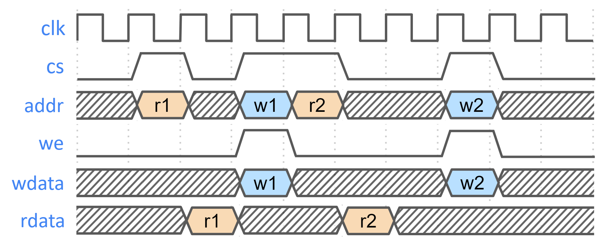
SRAM parameterization
Parameterization for ICCM/DCCM/I-Cache memories is derived from the configuration of the VeeR RISC-V core that has been selected for Caliptra Subsystem integration. Parameters defined in the VeeR core determine signal dimensions at the Subsystem top-level interface and drive requirements for SRAM layout. For details about interface parameterization, see the Interfaces & Signals section.
Example SRAM machine check reliability integration
This section describes an example implementation of integrator machine check reliability.
This example is applicable to scenarios where an integrator may need control of or visibility into SRAM errors for purposes of reliability or functional safety. In such cases, integrators may introduce additional layers of error injection, detection, and correction logic surrounding SRAMs. The addition of such logic is transparent to the correct function of Caliptra Subsystem, and removes integrator dependency on Caliptra Subsystem components for error logging or injection.
Note that the example assumes that data and ECC codes are in non-deterministic bit-position in the exposed SRAM interface bus. Accordingly, redundant correction coding is shown in the integrator level logic (i.e., integrator_ecc(caliptra_data, caliptra_ecc)). If the Caliptra Subsystem data and ECC are deterministically separable at the Caliptra Subsystem interface, the integrator would have discretion to store the ECC codes directly and calculate integrator ECC codes for the data alone.
Figure: Example machine check reliability implementation
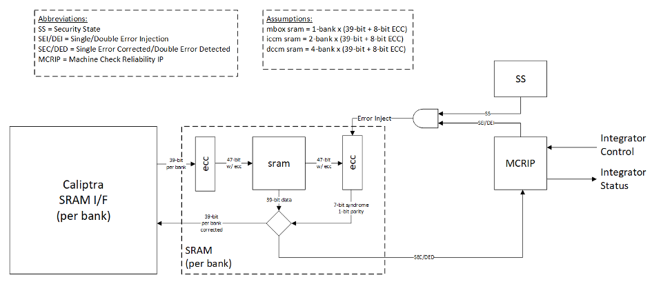
Error detection and logging
- Caliptra Subsystem IP shall interface to ECC protected memories.
- Caliptra Subsystem IP calculates and applies its own ECC code, which produces a total of 39-bit data written to external or INTEGRATOR instantiated SRAMs.
- Each 39-bit bank memory internally calculates 8-bit ECC on a write and stores 47 bits of data with ECC into SRAM.
- On read access syndrome is calculated based on 39-bit data.
- If parity error is detected and syndrome is valid, then the error is deemed single-bit and correctable.
- If no parity error is detected but syndrome == 0 or the syndrome is invalid, the error is deemed uncorrectable.
- On both single and double errors, the read data is modified before being returned to Caliptra Subsystem.
- Since single-bit errors shall be corrected through INTEGRATOR instantiated logic, Caliptra Subsystem never sees single-bit errors from SRAM.
- Double-bit or uncorrectable errors would cause unpredictable data to be returned to Caliptra Subsystem. Since this condition shall be detected and reported to MCRIP, there is no concern or expectation that Caliptra Subsystem will operate correctly after a double error.
- On detection, single errors are reported as transparent to MCRIP, double errors are reported as fatal.
- Along with error severity, MCRIP logs physical location of the error.
- After MCRIP logs an error, it has a choice to send out in-band notification to an external agent.
- MCRIP logs can be queried by SoC software.
Error injection
- MCRIP supports two error injection modes: intrusive and non-intrusive.
- Intrusive error injection:
- Can force a single or double error to be injected, which would result in incorrect data to be returned on read access.
- The intrusive error injection mode is disabled in Production fused parts via Security State signal.
- Non-intrusive error injection:
- Allows external software to write into MCRIP error log registers.
- The non-intrusive error injection does not interfere with the operation of memories.
- The non-intrusive error injection is functional in Production fused parts.
Caliptra Subsystem error handling flow
- Any implementation of error and recovery flows must adhere to the error handling requirements specified in Caliptra.md
- See MCI error handling for more details on MCI error infrastructure and error handling in Caliptra Subsystem.
- SoC level reporting and handling of fatal & non-fatal errors is product-specific architecture, outside the scope of Caliptra Subsystem definition. For example, a CPU and a PCIe device may handle fatal and non-fatal errors differently.
Programming interface
There are two primary programming avenues to interface with the Caliptra Subsystem:
-
MCU Firmware
- Description: This method involves programming the Microcontroller Unit (MCU) to execute firmware.
- Details: For more information on how to program the MCU and execute firmware via the MCU, please refer to the MCU Programming Interface documentation.
-
Caliptra Firmware
- Description: This method involves programming the Caliptra Core to execute firmware.
- Details: For more information on how to program and execute Caliptra Core firmware, please refer to the Caliptra Core References and Related Specifications.
Sequences
Reset Sequence:
- De-assert
cptra_ss_rst_b_iafter the primary clock (clk_i) stabilizes.
How to test
Reference tests are available at caliptra-ss\src\integration\test_suites
| Test Suite Name | Description |
|---|---|
MCU_HELLO_WORLD | Runs a basic "Hello World" program on the MCU to verify basic operation. |
MCU_CPTRA_BRINGUP | Tests the bring-up sequence of the MCU in the Caliptra Subsystem. |
MCU_DCCM_ACCESS | Validates access to the Data Closely Coupled Memory (DCCM) by the MCU. |
MCU_FUSE_CTRL_BRINGUP | Tests the bring-up sequence of the Fuse Controller by the MCU. |
MCU_LMEM_EXE | Tests execution by MCU from the MCU SRAM, contained inside the MCI component. LMEM refers to Local Memory, a generic alias for MCU SRAM. |
MCU_MCTP_SMOKE_TEST | Test verifies the I3C main target operation |
MCU_TEST_ROM_I3C_STREAMING_BOOT | Test verifies the I3C recovery target operation by using caliptra test ROM |
FUSE_PROV_WITH_LC_CTRL | Tests fuse provisioning in conjunction with the Lifecycle Controller. |
CALIPTRA_SS_LC_CTRL_BRINGUP | Tests the bring-up sequence of the Lifecycle Controller. |
CALIPTRA_SS_LC_CTRL_ST_TRANS | Validates state transitions of the Lifecycle Controller. |
Caliptra Core
Follow the link for Caliptra Core Integration Specification
MCU (Manufacturer Control Unit)
Overview
MCU is encapsulates VeeR EL2 core that includes an iCache, a dedicated DCCM, and AXI interfaces with separate AXI USER IDs to ROM and MCI. For more details refer to RISCV VeeR-EL2 Overview
Parameters & Defines
The VeeR EL2 core instance used for MCU has been configured with these options:
- DCCM size: 16KiB (see MCU DCCM SRAM Sizing)
- I-Cache depth: 16KiB
- ICCM: Disabled
- External Interrupt Vectors: 255
The following files from the Caliptra Subsystem repository contain the MCU configuration. Review these files for comprehensive list of MCU capabilities.
src/riscv_core/veer_el2/rtl/defines/css_mcu0_common_defines.vh
src/riscv_core/veer_el2/rtl/defines/css_mcu0_el2_param.vh
src/riscv_core/veer_el2/rtl/defines/css_mcu0_el2_pdef.vh
src/riscv_core/veer_el2/rtl/defines/defines.h
MCU Integration Requirements
-
Ensure Proper Memory Mapping
- The memory layout must match the physical memory configuration of the SoC.
- If modifications are required, update the base addresses and section placements accordingly.
- The address regions assigned to PIC and DCCM must not include any other AXI subordinates on the interconnect.
-
Enabling Programming interface.
- Please refer to section MCU Programming Interface for details on reference linker file for the MCU bringup.
MCU Core Configuration Customization
The MCU VeeR-EL2 core can be customized by integrators to optimize for specific SoC requirements.
Common Use Cases:
- Memory Architecture: Modify ICCM/DCCM addresses and sizes for SoC memory integration
- Power/Area Optimization: Remove or modify features (caching, number of interrupts)
- Performance Tuning: Adjust cache sizes and pipeline configurations for application workloads
Configuration Instructions:
Refer to the MCU Veer-EL2 Core Configuration section in the project README for complete step-by-step procedures.
Validation:
Execute the full regression test suite documented in How to test after any configuration changes to ensure system compatibility.
MCU DCCM SRAM Sizing
MCU's DCCM SRAM should be sized large enough to accommodate FW's stack and heap. If it is undersized, the MCU would have to rely on the MCU SRAM (accessed via AXI) for the stack/heap which has much lower performance.
MCU SRAM MRAC Considerations
The MCU's Memory Region Access Control (MRAC) regions are hard coded to 256MB boundaries. Each 256MB region is configured with uniform attributes - everything within a region is labeled as either "side effect" or "cachable". This affects how MCU SRAM and MCU MBOX SRAM (both located within MCI) should be integrated into the SoC memory map, as different components within MCI may require different access attributes.
Split Memory Mapping
Integrators have two main approaches for handling MCI memory mapping:
Option 1: Contiguous MCI Address Region - If integrators don't care about the MRAC limitations described in the following sections, they can use a standard contiguous MCI address map where all MCI components (including MCU SRAM and MCU MBOX SRAM) reside within a single 256MB region.
Option 2: Split Memory Mapping - Integrators can optionally split MCU SRAM and MCU MBOX SRAMs into their own dedicated 256MB regions, separate from other MCI components. This allows firmware to enable caching or disable side effects for these specific SRAMs.
Side Effect Considerations
When MCU SRAM and MCU MBOX SRAM remain within the main MCI address space (not split off), integrators should consider the following access limitations:
DWORD Access Requirement: MCI peripherals (MCI CSRs, MCU trace buffer CSRs, etc) require "side effect" attribute enabled. When "side effect" is enabled dword-aligned accesses are required. Unaligned accesses, like accessing a uint8_t, are not permitted and will result in a read fault error in the MCU.
If you want to avoid these DWORD alignment limitations and allow more flexible access patterns, you can choose to implement the Split Memory Mapping (Option 2) in your AXI interconnect for MCU SRAM and/or MCU MBOX SRAM. This allows the SRAMs to be placed in regions without the side effect attribute.
iCache Considerations
When MCU SRAM remains within the main MCI address space (not split off), integrators should consider the following caching limitations:
iCache Enablement Requirement: To enable MCU iCache, everything within the 256MB boundary containing MCU SRAM must be cachable. Since not all regions of MCI are cachable, MCU iCache cannot be enabled when using a contiguous MCI address map.
If you want to enable MCU iCache functionality, you must implement the Split Memory Mapping (Option 2) in your AXI interconnect. This allows MCU SRAM to be placed in a dedicated cachable region separate from other MCI components.
MCU Programming interface
MCU Linker Script Integration
This linker script defines the memory layout for the MCU firmware. It specifies the placement of various sections, ensuring proper memory mapping and execution flow.
Example Linker File can be found at : integration/test_suite/libs/riscv_hw_if/link.ld
By following this linker script configuration, the validation firmware can be correctly mapped and executed within the Caliptra Subsystem. Memory mapping for the validation firmware follows these principles:
- Instructions are stored in ROM for initial boot (.text)
- Read-only data is stored in ROM
- Stack and data sections are allocated to DCCM
- MCU SRAM is used for any combination of instructions and data to demonstrate program execution, data storage and persistence, streaming boot operations, and region protections that are enforced by MCI. Test firmware and corresponding linker scripts may be found in the repository test suites directory.
MCU External Interrupt Connections
| External interrupt vector | Description |
|---|---|
| 1 | MCI interrupts see MCI interrupt spec and MCI interrupt registers |
| 2 | I3C Interrupts |
| 255:3 | Exposed to SOC via cptra_ss_mcu_ext_int |
Fuse Controller
Overview
The Fuse Controller is a core component in the secure infrastructure of the system, responsible for managing the fuses and ensuring the integrity, consistency, and secure storage of sensitive data. It provides essential interfaces for direct fuse programming. The Fuse Controller interacts closely with the Lifecycle Controller (LC), FUSE macros, MCI, and Caliptra Core.
For an in-depth understanding of the Fuse Controller's functionality, including its programming flow, refer to Caliptra Subsystem Hardware Specification Document.
Parameters & Defines
| Parameter | Default | Description |
|---|---|---|
AlertAsyncOn | 5 | Enables asynchronous transitions on alerts. |
MemInitFile | "" | Hex file to initialize the OTP macro, including ECC. |
Interface
| Facing | Type | Width | Name | External Name in SoC Level | Description |
|---|---|---|---|---|---|
| External | Input | 1 | clk_i | cptra_ss_clk_i | Fuse Controller clock input. |
| External | Input | 1 | rst_ni | cptra_ss_rst_b_i | Reset signal input, active low. |
| Internal | Input | 1 | FIPS_ZEROIZATION_CMD_i | Fuse Zeroization request sampled on MCI reset deassertion. | |
| External | interface | 1 | core_axi_wr_req | cptra_ss_otp_core_axi_wr_req_i | AXI write request. |
| External | interface | 1 | core_axi_wr_rsp | cptra_ss_otp_core_axi_wr_rsp_o | AXI write response. |
| External | interface | 1 | core_axi_rd_req | cptra_ss_otp_core_axi_rd_req_i | AXI read request. |
| External | interface | 1 | core_axi_rd_rsp | cptra_ss_otp_core_axi_rd_rsp_o | AXI read response. |
| Internal | Output | 1 | intr_otp_operation_done_o | Indicates that the OTP operation has completed. | |
| Internal | Output | 1 | intr_otp_error_o | OTP error interrupt output (to be connected to MCI). | |
| Internal | Output | 5 | alerts | Alert signals for critical errors. | |
| Internal | Input | 1 | pwr_otp_i | OTP initialization request from the power manager. | |
| Internal | Output | Struct | pwr_otp_o | OTP response to the power manager. | |
| Internal | Input | Struct | lc_otp_vendor_test_i | Vendor test request input from LC Controller. | |
| Internal | Output | Struct | lc_otp_vendor_test_o | Vendor test response to LC Controller. | |
| Internal | Input | Struct | lc_otp_program_i | Lifecycle OTP programming request from LC Controller. | |
| Internal | Output | Struct | lc_otp_program_o | Lifecycle OTP programming response to LC Controller. | |
| Internal | Input | 1 | lc_dft_en_i | DFT enable input from LC Controller. | |
| Internal | Input | 1 | lc_escalate_en_i | Escalation enable input from LC Controller. | |
| Internal | Input | 1 | lc_check_byp_en_i | Clock bypass check enable input from LC Controller. | |
| Internal | Output | Struct | otp_lc_data_o | Lifecycle broadcasted data output to LC Controller. | |
| Internal | Output | Struct | otp_broadcast_o | FUSE broadcast output to Caliptra Core. This port broadcasts UDS-seed and Field-entropy-seed. |
Fuse Macro Memory Map and Fuse Controller CSR Address Map
The Caliptra Subsystem fuse controller supports a flexible and extensible memory map for storing one-time programmable (OTP) data. This structure is documented in the following files:
- Fuse Controller Register Map for registers.
- Fuse Macro Memory Map for fuse partition map.
The current fuse memory map consists of three main architectural segments: Caliptra-Core (prefix: CALIPTRA_CORE), Caliptra-Subsystem (prefix: CALIPTRA_SS), SoC/Vendor-Specific.
This structure enables separation of responsibilities and flexibility in SoC integration. While the Caliptra-Core fuse items are mandatory and must adhere to the Caliptra Fuse Map Specification, Caliptra-Subsystem fuses are required only when Caliptra is instantiated with Caliptra Subsystem. These Caliptra Subsystem fuses can also be configured based on SoC requirements. The SoC/Vendor-specific items can be customized based on integrator needs and product requirements. Therefore, the fields under SoC-specific categories can be resized or eliminated if unused.
SOC_SPECIFIC_IDEVID_CERTIFICATE Usage
This field defaults to 4 bytes but can be extended to accommodate storage of a full IDevID hybrid certificate (e.g., ML-DSA + ECC) if desired. Integrators must adjust its size in the YAML config used by the generation script.
FC Integration Requirements
Connectivity, Clock & Reset, Constraints & Violations
-
Connectivity:
- The Fuse Controller must interface seamlessly with the Fuse Macros, ensuring proper ECC support during programming and read operations.
- All AXI interfaces (
core_axi_wr_req,core_axi_rd_req) must follow the protocol specifications. - Inputs like
lc_otp_program_iandpwr_otp_ishould connect properly to the Lifecycle Controller (LC) and MCI respectively. - Alerts must propagate correctly to the system's alert manager for error handling.
-
Constraints & Violations:
- Any access to fuses must be gated by the
FUSE_CTRL_DIRECT_ACCESS_REGWENbit to prevent unauthorized writes. - There are some fuses that can be programmed only by Caliptra Core. Therefore, each AXI write should follow the access permission rule defined by
access_control_tableinsrc/fuse_ctrl/rtl/otp_ctrl_pkg.sv. - Timeout conditions during consistency checks (
FUSE_CTRL_CHECK_TIMEOUT) should trigger appropriate alerts. - Errors like invalid data, ECC failures, or access violations should raise alerts via the
alertssignal.
- Any access to fuses must be gated by the
-
Scan Path Exclusions:
- Ensure that secret fuse fields (UDS and Field-Entropy) and their corresponding flip-flops are not a parth of the scan path. Specifically, in this version, there are five OTP partitions that contain secrets that must not be leaked:
SECRET_MANUF_PARTITION: that contains the UDS seed, andSECRET_PROD_PARTITION_{0,1,2,3}: that each contain field entropy. These fuse partitions are "Buffered" partitions, meaning they are sensed at power-on and buffered in flip-flops until the next reset. During SoC integration it is vital to exclude the buffering flops that hold sensitive secret data from the scan chain to avoid leaks. These buffering flops may be excluded from the scan chain by excluding the following hierarchies:**::u_otp_ctrl::u_part_buf::u_otp_ctrl_ecc_reg::gen_partitions[X]::gen_buffered::u_part_buf::u_otp_ctrl_ecc_reg::**, for all values ofXin 1–5, since indices 1–5 map to the sensitive partitions mentioned above (defined in thePartInfolocalparam inotp_ctrl_part_pkg.sv, autogenerated from the OTP memory map HJSON). Additionally, these secrets are broadcasted with this input port:otp_broadcast_o. Therefore, this port, its propagated signals, and its driver signals must also not be scannable.
- Ensure that secret fuse fields (UDS and Field-Entropy) and their corresponding flip-flops are not a parth of the scan path. Specifically, in this version, there are five OTP partitions that contain secrets that must not be leaked:
- Since Fuse Controller scrambles secret partition with PRESENT chipher, this chiper keys, autogenerated from the OTP memory map HJSON, must be excluded from the scan path. Although these values are parameters defined in
otp_ctrl_part_pkg.sv, the registers driven by these parameters must be excluded from the scan path. - Note, the LC token partitions are not considered secret as only the cSHAKE128 hashes of each token are stored, not the raw tokens themselves.
- The Fuse Controller additionally implements three hardening mechanisms that protect the secret partition hardware digests: the physical debug-intent strap (
cptra_ss_debug_intent_i), which is sampled before Fuse Controller initialization; theSECRET_DIGEST_READ_LOCKFuse Controller CSR; and theSS_DEBUG_INTENT_MCUMCI register. The latter two are set by the MCU after Fuse Controller initialization. Only the strap additionally prevents the secret partitions' digests from being loaded into the partition buffers; the other two cannot. All three, however, ensure that there is no software path to read the digest fields through either the named CSR or the DAI. For more details, see Debug Intent Secret Zeroization. This is a defense-in-depth measure only: it does not remove the scan-path exclusion requirements above. The integrator must still exclude the secret buffering flops, the scrambler-key registers, and theotp_broadcast_osignals from the scan chain.
Direct Access Interface
Fuse macros has to be programmed via the Direct Access Interface, which is comprised of the following CSRs:
| CSR Name | Description |
|---|---|
DIRECT_ACCESS_WDATA_0 | Low 32bit word to be written. |
DIRECT_ACCESS_WDATA_1 | High 32bit word to be written. |
DIRECT_ACCESS_RDATA_0 | Low 32bit word that has been read. |
DIRECT_ACCESS_RDATA_1 | High 32bit word that has been read. |
DIRECT_ACCESS_ADDRESS | byte address for the access. |
DIRECT_ACCESS_CMD | Command register to trigger a read or a write access. |
DIRECT_ACCESS_REGWEN | Write protection register for DAI. |
When debug intent is asserted — or the SECRET_DIGEST_READ_LOCK CSR is set — a DAI read of a secret partition's hardware digest returns zero, and the corresponding named digest CSR returns only a provisioned indicator (all-ones if the sensed digest is provisioned/non-zero, otherwise zero) instead of the real digest. This applies to every secret partition that carries a hardware digest, including SECRET_LC_TRANSITION_PARTITION. See Debug Intent Secret Zeroization.
Initialization
The OTP controller initializes automatically upon power-up and is fully operational by the time the processor boots.
When debug intent is asserted via the physical strap (i.e., before this initialization), the zeroized secret partitions are not sensed and their buffer registers remain zero, while SECRET_LC_TRANSITION_PARTITION is sensed normally so the Life Cycle Controller can still transition; the controller still completes initialization. Debug intent asserted later through the SS_DEBUG_INTENT_MCU register does not change sensing (the partitions are already sensed) but still masks the digest reads. See Debug Intent Secret Zeroization.
The only initialization steps that SW should perform are:
- Check that the OTP controller has successfully initialized by reading
STATUS. I.e., make sure that none of the ERROR bits are set, and that the DAI is idle (STATUS.DAI_IDLE).- Choose whether the periodic background checks shall be subject to a timeout by programming a nonzero timeout cycle count to
CHECK_TIMEOUT. In this case, theCHECK_TIMEOUTregister must be set before theINTEGRITY_CHECK_PERIODandCONSISTENCY_CHECK_PERIODregisters (see next point). - Enable periodic background checks by programming nonzero mask values to
INTEGRITY_CHECK_PERIODandCONSISTENCY_CHECK_PERIOD. - It is recommended to lock down the background check registers via
CHECK_REGWEN, once the background checks have been set up
- Choose whether the periodic background checks shall be subject to a timeout by programming a nonzero timeout cycle count to
If needed, one-off integrity and consistency checks can be triggered via CHECK_TRIGGER.
If this functionality is not needed, it is recommended to lock down the trigger register via CHECK_TRIGGER_REGWEN.
Programming interface
The Fuse Controller (FC) programming interface is designed to manage lifecycle states, handle fuses with ECC support, and ensure secure interactions with the fuse macros. A key component in this architecture is the Fuse Controller Filter RTL. This module intercepts and verifies the fuse programming sequence by checking that all parts of the transaction originate from the same authorized source. In doing so, the filter guarantees that fuse provisioning is performed in an atomic manner.
Atomic fuse provisioning means that only one entity can initiate the programming sequence at a time. The entire sequence—data write, address write, and command write—must complete successfully. If any phase fails or if an inconsistency is detected (for example, if the AXI user ID changes between phases), the operation is aborted, and a cold reset is required before any new programming attempt can be made.
The access control table, which defines allowed fuse address ranges along with the corresponding authorized AXI user IDs. See access_control_table in src/fuse_ctrl/rtl/otp_ctrl_pkg.sv.
Below are the key operations supported by the programming interface:
-
Direct Access Interface (DAI):
- Registers:
FUSE_CTRL_DIRECT_ACCESS_CMD: Specifies the operation (FUSE_CTRL_CMD_DAI_WRITEfor write,FUSE_CTRL_CMD_DAI_READfor read).FUSE_CTRL_DIRECT_ACCESS_ADDRESS: Specifies the fuse memory address to access.FUSE_CTRL_DIRECT_ACCESS_WDATA_0: Write data (32-bit granularity).FUSE_CTRL_DIRECT_ACCESS_WDATA_1: Write data for 64-bit operations.FUSE_CTRL_DIRECT_ACCESS_RDATA_0: Read data (32-bit granularity).FUSE_CTRL_DIRECT_ACCESS_RDATA_1: Read data for 64-bit operations.
- Procedure:
- Write the address to
FUSE_CTRL_DIRECT_ACCESS_ADDRESS. - For write operations:
- Populate
FUSE_CTRL_DIRECT_ACCESS_WDATA_0(andFUSE_CTRL_DIRECT_ACCESS_WDATA_1for 64-bit operations).
- Populate
- Set the command in
FUSE_CTRL_DIRECT_ACCESS_CMD. - Wait for the operation to complete by polling the
DAI_IDLEbit inFUSE_CTRL_STATUS.
- Write the address to
- ECC Support:
- ECC is automatically applied during programming to ensure data integrity.
- Registers:
-
Digest Calculation:
- Used to lock a partition after programming is complete.
- Registers:
FUSE_CTRL_DIRECT_ACCESS_CMD: Use command0x4for digest calculation.FUSE_CTRL_DIRECT_ACCESS_ADDRESS: Partition base address.
- Procedure:
- Write the partition base address to
FUSE_CTRL_DIRECT_ACCESS_ADDRESS. - Trigger the digest calculation command (
0x4) inFUSE_CTRL_DIRECT_ACCESS_CMD. - Poll the
DAI_IDLEbit inFUSE_CTRL_STATUSto confirm the operation is complete.
- Write the partition base address to
Readout Sequence
A typical readout sequence looks as follows:
- Check whether the DAI is idle by reading the
STATUSregister. - Write the byte address for the access to
DIRECT_ACCESS_ADDRESS. Note that the address is aligned with the granule, meaning that either 2 or 3 LSBs of the address are ignored, depending on whether the access granule is 32 or 64bit. - Trigger a read command by writing 0x1 to
DIRECT_ACCESS_CMD. - Poll the
STATUSuntil the DAI state goes back to idle. Alternatively, theotp_operation_doneinterrupt can be enabled up to notify the processor once an access has completed. - If the status register flags a DAI error, additional handling is required.
- If the region accessed has a 32bit access granule, the 32bit chunk of read data can be read from
DIRECT_ACCESS_RDATA_0. If the region accessed has a 64bit access granule, the 64bit chunk of read data can be read from theDIRECT_ACCESS_RDATA_0andDIRECT_ACCESS_RDATA_1registers. - Go back to the first step and repeat until all data has been read.
The hardware will set DIRECT_ACCESS_REGWEN to 0x0 while an operation is pending in order to temporarily lock write access to the CSRs registers.
Sequences: Reset, Boot
-
Reset Sequence:
- De-assert
rst_niafter the primary clock (clk_i) stabilizes. - Verify reset state by reading
FUSE_CTRL_STATUS. All errors in the status register should be 0. - Ensure Fuse Macros are in their default state after reset.
- De-assert
-
Boot Sequence:
- Initialize Fuse Macros by programming essential fuses using the programming interface.
- Perform a full integrity check by triggering
FUSE_CTRL_CHECK_TRIGGERand ensure the system is error-free before proceeding. - Validate readiness by checking the
FUSE_CTRL_STATUSregister.
UDS & Field Entropy FIPS Zeroization Sequence
This sequence follows the "theory of operation" stated in this 'fuse-zeroization-programmer's-guide'
Follow these steps in order to correctly zeroize the fuses and verify the operation for any partition that requires FIPS zeroization to be set (determined by zeroizable flag when a partition is generated).
- Assert Physical Presence: Set the FIPS_zeroization_PPD pin high before taking the Caliptra subsystem out of reset. This confirms physical presence and authorizes the zeroization. When this signal is asserted, it triggers preemptive zeroization of secret FUSEs. The MCU ROM samples
cptra_ss_FIPS_ZEROIZATION_PPD_iby reading the corresponding register storing its value in MCI. Ifcptra_ss_FIPS_ZEROIZATION_PPD_i == HIGH, the MCU ROM writes32'hFFFF_FFFFto thess_soc_MCU_ROM_zeroization_mask_regregister of MCI. If this mask register is not set by MCU, the zeroization request is aborted by the fuse controller. - Issue Zeroization Commands: Trigger zeroization by sending a zeroization command to Caliptra core. Caliptra core will send a sequence of DAI (Direct Access Commands) commands to the fuse controller to perform the zeroization. The recommended order is:
- Clear the Partition Zeroization Flag: First, send a DAI command to clear this 64-bit flag within the target partition. Executing this step first is critical, as it masks potential ECC or integrity errors if the process is interrupted by a power failure.
- Zeroize Data Words: Send DAI zeroization commands for all data words within the partition.
- Clear the Partition Digest: Finally, send a DAI command to clear the partition's digest.
- Power Cycle the SOC (including Caliptra SS): Apply a cold reset to the Caliptra subsystem. FIPS_zeroization_PPD pin should now be cleared (set low).
- Verify the Operation: From the main MCU, read the partition's digest value from the associated fuse_ctrl digest registers.
- Success: If the register returns the expected zeroized digest value, the operation is complete.
- Failure: If the digest does not match the zeroized value, repeat the entire sequence starting from Step 1.
FIPS Zeroization Sequence For ECC
Zeroization is implemented within the fuse controller RTL module. It is therefore the integrator’s responsibility to ensure that the ECC bits in the corresponding fuse partition are also zeroized when a zeroization command is issued to the fuse macro. To achieve this, the integrator must provide a dedicated implementation in the fuse macro wrapper to handle zeroization of the ECC bits.
Miscellanious Fuse Integration Guidelines
- If there is a provisioning step where SW (non-secret) and secret partitions need to be programmed within the same reset/power cycle of a SOC, then SW partition needs to be programmed first
- Whenever a secret partition is programmed, it requires a FC reset, implying it requires a SOC reset
- ECC bits inside fuse macros MUST be zeroized per FIPS guidelines. Since these bits are implemented by SOC a a part of OTP gasket, SOC should also implement FIPS zeroization of the ECC for UDS, FE, Ratchet Seeds (OCP lock), any vendor secrets (if required by FIPS).
- FIPS zeroization of the ECC bits of a given partition must be done after the FIPS zeroization of the partition data, zeroization marker and digest.
- UDS & FE MUST ONLY be FIPS zeroized by Caliptra Core (by Subsystem default design construction doesnt allow anyone else to do this operation).
- DAI Command Error Checking: The Caliptra core is responsible for checking the result of each DAI zeroization command to ensure it completed successfully. Any errors must be handled appropriately.
- Partitions 0-5 should not be changed by SOC. Don’t add or remove any fields, re-adjust sizes of these partitions as Caliptra ROM may expect them to be of a fixed size.
- Fuse Macro Wrapper Requirements: The fuse_ctrl macro wrapper must implement a retry mechanism for the zeroization process. To prevent damage to the fuses, the wrapper must also avoid double writes to bits that have already been programmed. Please follow the specific integration guidelines provided by your fuse macro vendor.
- OCP Lock ratchet seeds can be FIPS zeroized by MCU
- If FIPS zeroization is required for Vendor Secret Partitions, then SOC shall generate the partition with zeroization flag, validate that the zeroization sequence documented above works as expected and uses MCU to do the FIPS zeroization. Any additional physical security protection of this partition is SOC's responsibility since the use cases are SOC defined.
How to test : Smoke & more
The smoke test focuses on ensuring basic functionality and connectivity of the FC & LCC.
Generating the Fuse Partitions
The configurable parts of the fuse_ctrl, specifically the fuse map and register interface,
are bootstrapped through a separate script ./tools/scripts/fuse_ctrl_script/gen_fuse_ctrl_partitions.py.
For a detailed breakdown of the design rationale behind the script as well as execution instructions,
refer to Fuse Map Generation Script.
Fuse Controller Macro
The following integration section is based on the Generalized Open-source Interface with modifications to match the Caliptra implementation.
Overview
The Fuse Controller Macro implements a generalized open-source interface for functional operation (described below). Any OTP redundancy mechanism like per-word ECC is assumed to be handled inside the wrapper, which means that the word width exposed as part of the generalized interface is the effective word width.
Paramteres & Defines
| Parameter | Default | Description |
|---|---|---|
Width | 16 | Width of native OTP words. |
AddrWidth | Derived | Width of the address signal, derived from Depth. |
Depth | `2**OtpAddrWidth | Depth of OTP macro. |
CmdWidth | 7 | Width of the OTP command. Sparsely encoded. |
ErrWidth | 3 | Width of error code output signal. |
SizeWidth | 2 | Width of the size input field. Allows to transfer up to 4 native OTP words at once. |
PwrSeqWidth | "" | Hex file to initialize the OTP macro, including ECC. |
IfWidth | 2**OtpSizeWidth*OtpWidth | Width of the wrapper data interface. |
FC Macro Integration Requirements
The generalized open-source interface is a simple command interface with a ready / valid handshake that makes it possible to introduce back pressure if the OTP macro is not able to accept a command due to an ongoing operation.
In order to facilitate the scrambling and digest operations, the data width has been sized such that data blocks up to the PRESENT block size (64bit) can be transferred across the generalized interface. The actual size of a transfer is determined via the size_i field. Transfer sizes are specified in multiples of the native OTP block size, as listed below.
Value of size_i | #Native OTP Words | Bit Slice |
|---|---|---|
| 2'b00 | 1 | {word0} = data[15:0] |
| 2'b01 | 2 | {word1, word0} = data[31:0] |
| 2'b10 | 3 | {word2, word1, word0} = data[47:0] |
| 2'b11 | 4 | {word3, word2, word1, word0} = data[63:0] |
Responses are returned in-order via an unidirectional response interface (i.e., without back pressure capability). Downstream logic must be able to sink the response in any case. The response optionally carries read data, depending on whether the operation that took place was a read or not. Also, an error signal returns a non-zero error code in case an error occurred while carrying out the OTP command.
The signals pertaining to the generalized open-source interface are listed below.
The signals are exposed as cptra_ss_fuse_macro_outputs_i and
cptra_ss_fuse_macro_inputs_o at the top level.
| Signal | Type | Width | Description |
|---|---|---|---|
cptra_ss_fuse_macro_inputs_o.valid_i | Input | 1 | Valid signal for the command handshake. |
cptra_ss_fuse_macro_inputs_o.size_i | Input | [SizeWidth-1:0] | Number of native OTP words to transfer, minus one: 2'b00 = 1 native word ... 2'b11 = 4 native words. |
cptra_ss_fuse_macro_inputs_o.cmd_i | Input | [CmdWidth-1:0] | OTP command: 7'b1111010 = read, 7'b1001001 = write, 7'b1010100 = read raw, 7'b1100111 = write raw, 7'b0100000 = initialize, 7'b0111101 = zeroize |
cptra_ss_fuse_macro_inputs_o.addr_i | Input | [$clog2(Depth)-1:0] | OTP word address. |
cptra_ss_fuse_macro_inputs_o.wdata_i | Input | [IfWidth-1:0] | Write data for write commands. |
cptra_ss_fuse_macro_outputs_i.fatal_alert_o | Output | 1 | Fatal alert output from the FC macro. This is connected to a separate alert channel in the instantiating IP. The instantiating IP latches the alert indication and continuously outputs alert events until reset. |
cptra_ss_fuse_macro_outputs_i.ecov_alert_o | Output | 1 | Recoverable alert output from the FC macro. This is connected to a separate alert channel in the instantiating IP. Should only be pulsed high for each alert occurrence. The instantiating IP then sends out a single alert event for each pulse. |
cptra_ss_fuse_macro_outputs_i.ready_o | Output | 1 | Ready signal for the command handshake. |
cptra_ss_fuse_macro_outputs_i.valid_o | Output | 1 | Valid signal for command response. |
cptra_ss_fuse_macro_outputs_i.rdata_o | Output | [IfWidth-1:0] | Read data from read commands. |
cptra_ss_fuse_macro_outputs_i.err_o | Output | [ErrWidth-1:0] | Error code. |
The write raw and read raw command instructs the Fuse Controller Macro
wrapper to store / read the data in raw format without generating nor checking
integrity information. That means that the wrapper must return the raw,
uncorrected data and no integrity errors.
The zeroize command instructs the Fuse Macro wrapper to "erase" the addressed
value. As fuses cannot be unset, the typical erase behavior is to set all fuses
of the addressed value to 1, ideally including the ECC bits.
The Fuse Controller Macro wrapper implements the error codes (0x0 - 0x4).
| Error Code | Enum Name | Recoverable | DAI | LCI | Unbuf | Buf | Description |
|---|---|---|---|---|---|---|---|
| 0x0 | NoError | - | x | x | x | x | No error has occurred. |
| 0x1 | MacroError | no | x | x | x | x | Returned if the OTP macro command did not complete successfully due to a macro malfunction. |
| 0x2 | MacroEccCorrError | yes | x | - | x | x | A correctable ECC error has occurred during a read operation in the OTP macro. |
| 0x3 | MacroEccUncorrError | no | x | - | x* | x | An uncorrectable ECC error has occurred during a read operation in the OTP macro. Note (*): This error is collapsed into MacroEccCorrError if the partition is a vendor test partition. It then becomes a recoverable error. |
| 0x4 | MacroWriteBlankError | yes / no* | x | x | - | - | This error is returned if a write operation attempted to clear an already programmed bit location. Note (*): This error is recoverable if encountered in the DAI, but unrecoverable if encountered in the LCI. |
The timing diagram below illustrates the timing of a command. Note that both read and write commands return a response, and each command is independent of the previously issued commands. The latency from accepting a command to returning a response depends on the underlying OTP IP and is typically larger than 10 cycles. The returned values depend on the command type and whether an error occurred or not.
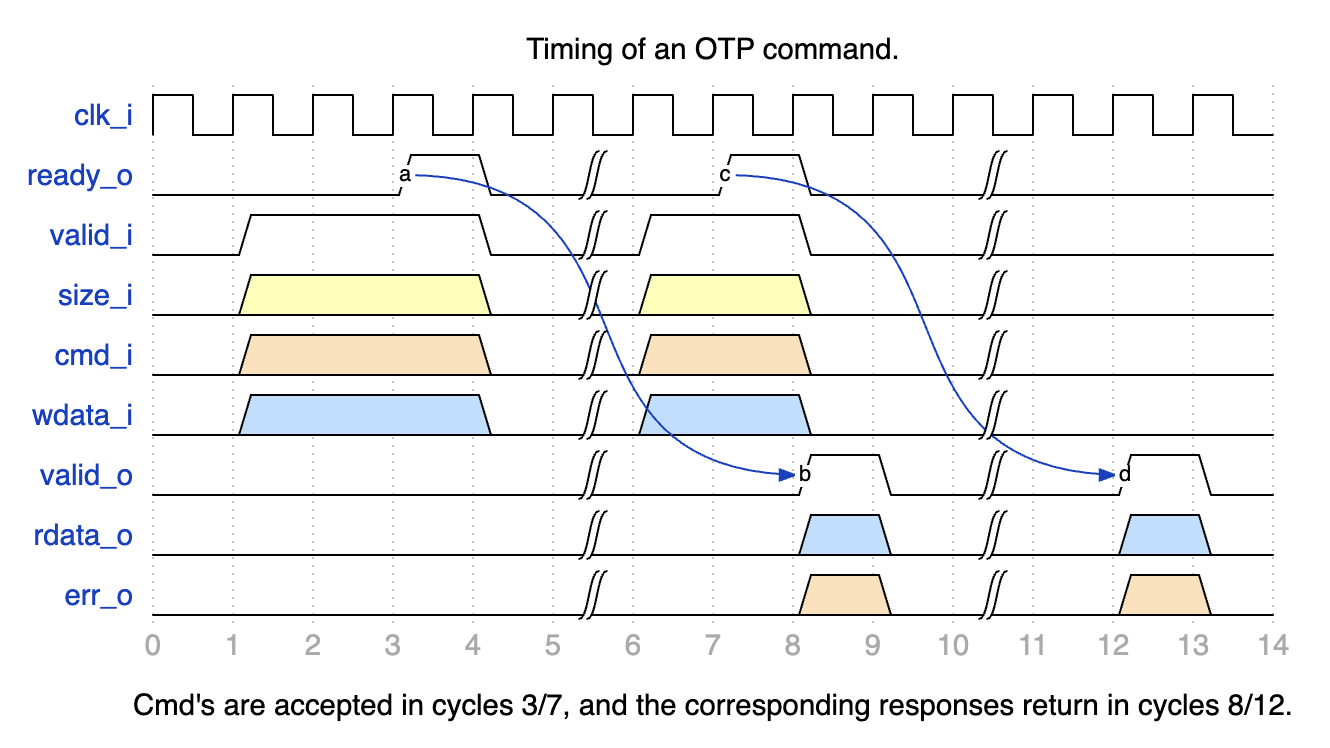
Note that the default configuration of the Fuse Controller allows up to two outstanding OTP commands, meaning that it is permissible to acknowledge an incoming command and start working on it while the results of the last command are still in the process of being output (e.g., due to an output register stage).
The Fuse Controller Macro uses the following signals to interface with the Fuse Controller.
Generic Strap Port Usage for FC Register Locations
To support flexible integration across varying fuse partition generations, Caliptra ROM uses two generic strap ports to locate fuse controller registers.
Why These Straps Are Needed
Each fuse partition generation introduces new error bits into the status register. This causes the idle bit to shift leftward, changing its position within the SOC_OTP_CTRL_STATUS register. Similarly, the CMD register may shift downward in memory if new fuse partition definitions introduce additional registers like ADDR, WDATA0, RDATA0, etc.
Because of these dynamic shifts:
- The idle bit location cannot be hardcoded.
- The CMD register address must be explicitly provided, even though the other fuse controller registers are laid out consecutively.
Strap Definitions
-
cptra_ss_strap_generic_0_i
A 32-bit input strap that encodes:- Upper 16 bits: Bit index of the idle status bit (
IDLE_BIT_STATUS) withinSOC_OTP_CTRL_STATUS. - Lower 16 bits: Offset address of
SOC_OTP_CTRL_STATUSwithin theSOC_IFC_REGspace, relative toSOC_OTP_CTRL_BASE_ADDR.
This allows the ROM to accurately monitor the fuse controller's idle state regardless of partition-induced shifts.
- Upper 16 bits: Bit index of the idle status bit (
-
cptra_ss_strap_generic_1_i
A 32-bit input strap that provides the address of the CMD register.
Since the fuse controller registers are laid out consecutively, specifying the CMD register is sufficient for the ROM to infer the locations of adjacent registers likeADDR,WDATA0, andRDATA0.
FC Macro Test Interface
The Fuse Controller Macro requires a test interface to be able to access the underlying OTP debug access interface and power manager controller. During early manufacturing, the test interface can be used to run BIST and repair flows before performing a non-volatile raw unlock operation.
For security reasons, it must be ensured that it is not possible to read / program arbitrary OTP memory locations through the test interface. Only specific, pre-defined test locations shall be readable and programmable. Access to debug access interface must also be disabled once the device is in mission mode (i.e. PROD life cycle state).
Life Cycle OTP Programming Behavior and Integrator Responsibilities
During a life‑cycle transition, the Caliptra Life Cycle Controller performs two OTP write operations to the transition‑counter and life‑cycle‑state fields. This behavior is architecturally defined and required for secure, fault‑resistant state progression. Although only one field changes in each phase, both fields reside within the same OTP word, so the macro receives two programming operations that may include writing some bits to the same value they already hold. This programming pattern is expected and safe for OTP implementations that correctly support word‑level writes, including rewriting a bit with the same value (1 -> 1).
Integrators must ensure that their OTP macro or wrapper supports rewriting fields without generating errors, and that the macro’s burn semantics align with Caliptra’s assumption that “burn” corresponds to writing a logical 1. If an OTP vendor interprets 0 as a burn operation or cannot tolerate 1 -> 1 writes, the integrator must adapt their wrapper—for example, by inverting the encoding or using per‑bit write‑enable—to ensure compatibility.
Life Cycle Controller
Overview
The LC Controller (Lifecycle Controller) is a critical component of the Caliptra Subsystem, responsible for securely managing the lifecycle states of the chip. The LC Controller interacts with other subsystems such as the Fuse Controller, MCI, AXI interconnect, and JTAG TAP to enforce secure transitions, validate tokens, and generate error conditions. Additionally, it implements escalation mechanisms to respond to security breaches, enabling the chip to enter secure states like SCRAP.
For a detailed description of the Lifecycle Controller's architecture, design, and operational flow, refer to Caliptra Subsystem Hardware Specification Document.
Parameters & Defines
| Parameter | Default (Max) | Description |
|---|---|---|
AlertAsyncOn | 2'b11 | |
IdcodeValue | 32'h00000001 | Idcode for the LC JTAG TAP. |
RndCnstLcKeymgrDivInvalid | (see RTL) | Diversification value used for all invalid life cycle states. |
RndCnstLcKeymgrDivTestUnlocked | (see RTL) | Diversification value used for the TEST_UNLOCKED* life cycle states. |
RndCnstLcKeymgrDivDev | (see RTL) | Diversification value used for the DEV life cycle state. |
RndCnstLcKeymgrDivProduction | (see RTL) | Diversification value used for the PROD/PROD_END life cycle states. |
RndCnstLcKeymgrDivRma | (see RTL) | Diversification value used for the RMA life cycle state. |
Interface
| Facing | Type | width | Name | External Name in SoC Level | Description |
|---|---|---|---|---|---|
| External | input | 1 | clk_i | cptra_ss_clk_i | clock |
| External | input | 1 | rst_ni | cptra_ss_rst_b_i | LC controller reset input, active low |
| External | input | 1 | lc_sec_volatile_raw_unlock_en_i | cptra_ss_lc_sec_volatile_raw_unlock_en_i | Enables Volatile TEST_UNLOCKED0 state transition infra |
| External | input | 1 | raw_unlock_token_hashed_i | cptra_ss_raw_unlock_token_hashed_i | Hashed token for RAW unlock |
| External | input | 1 | Allow_RMA_or_SCRAP_on_PPD | cptra_ss_lc_Allow_RMA_or_SCRAP_on_PPD_i | This is GPIO strap pin. This pin should be high until LC completes its state transition to RMA or SCRAP. |
| External | interface | 1 | axi_wr_req | cptra_ss_lc_axi_wr_req_i | LC controller AXI write request input |
| External | interface | 1 | axi_wr_rsp | cptra_ss_lc_axi_wr_rsp_o | LC controller AXI write response output |
| External | interface | 1 | axi_rd_req | cptra_ss_lc_axi_rd_req_i | LC controller AXI read request input |
| External | interface | 1 | axi_rd_rsp | cptra_ss_lc_axi_rd_rsp_o | LC controller AXI read response output |
| External | interface | 1 | jtag_i | cptra_ss_lc_ctrl_jtag_i | LC controller JTAG input ports |
| External | interface | 1 | jtag_o | cptra_ss_lc_ctrl_jtag_o | LC controller JTAG output ports |
| External | input | 1 | scan_rst_ni | cptra_ss_lc_ctrl_scan_rst_ni_i | LC controller scan reset input, active low |
| Internal | output | 3 | alerts | Alert outputs generated by LCC if there is an error due to one of following: register bus, lc state and fuse programming | |
| External | input | 1 | esc_scrap_state0 | cptra_ss_lc_esclate_scrap_state0_i | An escalation input that leads LC controller to enter into SCRAP mode |
| External | input | 1 | esc_scrap_state1 | cptra_ss_lc_esclate_scrap_state1_i | An escalation input that eads LC controller to enter into SCRAP mode |
| Internal | input | 1 | pwr_lc_i | A power initilization input coming from MCI | |
| Internal | struct | 1 | pwr_lc_o | Two outputs show: (i) LC controller can accept a request, (ii) LC is initialized. | |
| Internal | struct | 1 | lc_otp_vendor_test_o | Access to fuse controller for vendor test partitions | |
| Internal | struct | 1 | lc_otp_vendor_test_i | Access to fuse controller for vendor test partitions | |
| Internal | struct | 1 | lc_otp_program_o | Programming interface to fuse controller to update LCC state and couter | |
| Internal | struct | 1 | lc_otp_program_i | Programming interface from fuse controller to update LCC state and couter | |
| Internal | struct | 1 | otp_lc_data_i | Broadcasted values from the fuse controller | |
| Internal | output | 1 | lc_dft_en_o | DFT enable to MCI | |
| Internal | output | 1 | lc_hw_debug_en_o | CLTAP enable to MCI | |
| Internal | output | 1 | lc_escalate_en_o | cptra_ss_lc_escalate_en_o | Broadcast signal to promote esclation in SoC |
| Internal | output | 1 | lc_check_byp_en_o | cptra_ss_lc_check_byp_en_o | External clock status delivery signal to fuse controller |
| External | output | 1 | lc_clk_byp_req_o | cptra_ss_lc_clk_byp_req_o | A request port to swtich from LCC clock to external clock |
| External | input | 1 | lc_clk_byp_ack_i | cptra_ss_lc_clk_byp_ack_i | Acknowledgment signal to indicate external clock request is accepted |
| Internal | input | 1 | otp_device_id_i | Unused port | |
| Internal | input | 1 | otp_manuf_state_i | Unused port | |
| Internal | output | 1 | hw_rev_o | Unused port | |
| Internal | input | 253 | cptra_ss_mcu_ext_int | Reflection of HW revision ID read from fuse controller |
Fuse Macro Memory Map / Fuse Controller CSR Address Map
See Life-cycle Controller Register Map.
LC Integration Requirements
Connectivity, Clock & Reset, Constraints & Violations
-
Connectivity:
- Ensure proper routing of all signals to avoid conflicts with other modules.
- Interfaces like
jtagandaximust adhere to the defined protocol specifications. - Escalation signals (
esc_scrap_state0andesc_scrap_state1) brings LC controller into temporal SCRAP mode (Escalation state) and therefore needs to be connected to a dedicated controller. Allow_RMA_or_SCRAP_on_PPDneeds to be tied 0 if it is not being used. Otherwise, it might break LC controller's internal FSM.- Avoid glitches on
Allow_RMA_or_SCRAP_on_PPDand escalation inputs (esc_scrap_state0,esc_scrap_state1) that could cause unintended transitions. - Verify that all output signals, including alerts, remain within the expected ranges under normal operation.
-
IMPORTANT SOC REQUIREMENT:
- Life cycle controller allows you to switch from internal to external clock on a request from SOC over JTAG or AXI (As explained in other sections, this is typically used for Fuse programming scenarios when a stable clock is not yet available within the SOC). When the request arrives, life cycle controller requests the SOC to do the clock switch. When such a request is made, SOC MUST respond with an acknowledgement within 2 clock cycles of the internal clock. If this condition is not met, OTP controller will assert "program error" and the SOC must go through a reset cycle and redo the above steps. This must be verified by the SOC as a part of Caliptra subsystem integration checks.
To protect from clock stretching attacks Caliptra mandates using a clock source that is constructed within the SOC (eg. PLL, Calibrated Ring Oscillator, etc). For such a clock source, a SOC may require fuses to be programmed. TP programming demands a reliable and deterministic clock signal to ensure correct fuse write operations; which SOC may not have during the early phases of manufacturing flow due to above constraints. In order to overcome this issue, this
external clockcan be used typically in the manufacturing phase of a SOC; and for such SOCs this external clock is supplied from a platform (e.g an ATE). Since the Caliptra subsystem includes only one clock input (cptra_ss_clk_i), the SoC integrator is responsible for ensuring that this input can be switched to a stable source.The Life-cycle Controller requires a token to execute conditional state transitions. All tokens reside within a single partition, which the integrator can lock only once. Therefore, if any required tokens are not programmed before the partition is locked, they will remain at their default value of 0 and cannot be updated afterward.
- The life-cycle controller exposes an
LC_STATEregister that carries the life-cycle controller state, which the SoC can read to determine the current life-cycle state. In addition, the Caliptra Subsystem top level provides thecaliptra_ss_life_cycle_steady_state_oandcaliptra_ss_otp_state_valid_osignals, which are broadcast from the fuse controller. Whenevercaliptra_ss_otp_state_valid_ois asserted,caliptra_ss_life_cycle_steady_state_oreflects the latest life-cycle state stored in the fuse macro in the following cycle. Because the fuse controller is initialized earlier than the life-cycle controller, these broadcast state signals are derived from the fuse controller. Note thatcaliptra_ss_otp_state_valid_ois driven low by the fuse controller if a fatal error occurs in the fuse controller or if an escalation signal is asserted by the life-cycle controller. In contrast,LC_STATEprovides the life-cycle controller’s own view of the state, independent of the fuse controller’s errors such as entering SCRAP state.
Volatile-unlock state transitions are not reflected by the fuse controller, and therefore
caliptra_ss_life_cycle_steady_state_oandcaliptra_ss_otp_state_valid_odo not capture state transitions granted exclusively by the life-cycle controller. To cover this case, the Caliptra Subsystem also broadcastscaliptra_ss_volatile_raw_unlock_success_o, which is asserted by the life-cycle controller to indicate that the volatile-unlock state has been granted. -
Scan Path Exclusions:
- Ensure that the RAW_UNLOCK token is excluded from the scan chain. This token differs from other LC transition tokens because it is stored in gates, although it is also stored in a hashed form similar to other tokens. It is recommended to exclude since it is not provisioned through fuse macro as other tokens.
To exclude it from scan, the following hierarchies must be excluded:
*::lc_ctrl_fsm::hashed_tokens_{higher, lower}[RawUnlockTokenIdx]and*::lc_ctrl_fsm::hashed_token_mux.
- Ensure that the RAW_UNLOCK token is excluded from the scan chain. This token differs from other LC transition tokens because it is stored in gates, although it is also stored in a hashed form similar to other tokens. It is recommended to exclude since it is not provisioned through fuse macro as other tokens.
To exclude it from scan, the following hierarchies must be excluded:
-
RAW Unlock Token:
- The
cptra_ss_raw_unlock_token_hashed_itop-level input defines the hashed value of the RAW unlock token. The hashed value is generated from the unhashed RAW unlock token, which the integrator must obtain from a cryptographically secure random number generator. Both the hashed and the unhashed token must be kept secret. To generate the hashed token (and optionally also the unhashed token),tools/scripts/lc_ctrl_script/gen_lc_ctrl_token.pycan be used. - The unhashed RAW unlock token is required in SW that performs a non-volatile RAW unlock.
- The hashed RAW unlock token is stored in HW (see first bullet point) and required in SW that performs a volatile RAW unlock.
- The
Programming Interface
The LC Controller's programming interface facilitates lifecycle state transitions, secure token authentication, and system initialization. Below are the key programming steps:
-
Initialization:
- Ensure the LC Controller is ready by polling the
LC_CTRL_STATUS_OFFSETregister for theREADY_MASKbit. - Verify initialization is complete using the
INIT_MASKbit in the same register. - Corresponding fuse partitions need to be provisioned in order to perform state transitions
- Ensure the LC Controller is ready by polling the
-
Lifecycle State Transitions:
- Claim the transition mutex by writing
0x96(MuBi8True) toLC_CTRL_CLAIM_TRANSITION_IF_OFFSETand polling until the value is correctly latched. - Set the desired next lifecycle state by writing to
LC_CTRL_TRANSITION_TARGET_OFFSET. - Write the 128-bit transition token (if required) into the
LC_CTRL_TRANSITION_TOKEN_*_OFFSETregisters. - Trigger the state transition by writing
0x1toLC_CTRL_TRANSITION_CMD_OFFSET. - Poll the
LC_CTRL_STATUS_OFFSETregister to monitor for successful state transition or detect errors such as token errors, OTP errors, or RMA strap violations. - Each TEST_UNLOCKED state has its own TOKEN (see See Fuse Memory Map).
- During a state transition, an asserted reset or zeorization command can cause permanent life-cycle state corruption.
- Claim the transition mutex by writing
-
Token Validation:
- For conditional state transitions, provide the transition token before the transition request.
- Token format and fuse provisioning are illustrated with a python implementation:
from Crypto.Hash import cSHAKE128

# Raw (unhashed) token as a 128-bit integer
value = 0x318372c87790628a05f493b472f04808
data = value.to_bytes(16, byteorder='little')
# data (byte-array) = [0x08, 0x48, 0xf0, 0x72, 0xb4, 0x93, 0xf4, 0x05,
#                      0x8a, 0x62, 0x90, 0x77, 0xc8, 0x72, 0x83, 0x31]

custom = 'LC_CTRL'.encode('UTF-8')
shake = cSHAKE128.new(data=data, custom=custom)
hashed_token = shake.read(16)
# hashed_token (byte-array) = [0xad, 0x5a, 0x3d, 0x23, 0xa0, 0xd8, 0xe7, 0x26,
#                               0xd5, 0x74, 0x84, 0xa6, 0x68, 0xa0, 0x9c, 0x4c]
# hashed_token as big-endian hex = 0x4c9ca068a68474d526e7d8a0233d5aad
#
# HKMS must provision this hashed_token byte-array into the corresponding
# fuse location in SECRET_LC_TRANSITION_PARTITION via the DAI.

# To unlock a state having the shake condition above, the LCC needs
# to get the following raw token input set:
TOKEN_write(LC_CTRL_TRANSITION_TOKEN_0_OFFSET, 0x72f04808)
TOKEN_write(LC_CTRL_TRANSITION_TOKEN_1_OFFSET, 0x7790628a)
TOKEN_write(LC_CTRL_TRANSITION_TOKEN_2_OFFSET, 0x05f493b4)
TOKEN_write(LC_CTRL_TRANSITION_TOKEN_3_OFFSET, 0x318372c8)
- RMA and SCRAP Strap Handling:
- Ensure the
Allow_RMA_or_SCRAP_on_PPDGPIO strap is asserted for RMA or SCRAP transitions. Transitions without this strap will fail with an appropriate status in theLC_CTRL_STATUS_OFFSETregister.
- Ensure the
Sequences: Reset, Boot
-
Reset Sequence:
- Bring the LC Controller out of reset by asserting and de-asserting
rst_niafter clock stabilization. - Perform a reset sequence after each state transition routine
- Bring the LC Controller out of reset by asserting and de-asserting
-
Boot Sequence:
- Enable MCI that intilaize the LC controller.
- Verify successful initialization by reading
LC_CTRL_STATUS_OFFSET.
-
Error Scenarios:
- Test scenarios where invalid tokens, Fuse errors, or missing RMA straps are injected to validate error handling and system recovery mechanisms.
-
MCI Masking Registers for LCC Decoding Signals:
- The MCI provides a set of masking registers that allow the SoC integrator to explicitly masks Caliptra Core–debug level, SOC_DFT_EN and SOC_HW_DEBUG_EN. Caliptra Core expresses its debug grant through the
ss_soc_dbg_unlock_level_ivector, where each bit represents a distinct debug unlock level. These requests are not acted upon directly; instead, they are first AND-masked with SoC-programmed MCI registers to ensure that only integrator-approved debug levels can be enabled. - For production debug unlock, the integrator must program
MCI_REG_SOC_PROD_DEBUG_STATE_0andMCI_REG_SOC_PROD_DEBUG_STATE_1MCI registers. Together, these registers form a 64-bit mask that gatesss_soc_dbg_unlock_level_i. A debug level is considered enabled only if the corresponding bit is set both in Caliptra Core’s unlock request vector and in the SoC-programmed mask. For example, if Caliptra Core asserts the fifth debug level by settingss_soc_dbg_unlock_level_i[4], the integrator must also set bit ofMCI_REG_SOC_PROD_DEBUG_STATE[1:0][4]for that level to take effect. - The same masking mechanism applies to SOC_DFT_EN enable and SOC_HW_DEBUG_EN. For these, MCI offers
MCI_REG_SOC_DFT_EN_0,MCI_REG_SOC_DFT_EN_1andMCI_REG_SOC_HW_DEBUG_EN_0,MCI_REG_SOC_HW_DEBUG_EN_1mask registers. These are also masked withss_soc_dbg_unlock_level_i. If this masking (AND operation) results in a value that has1in it. The corresponding enable signal is set to high.
- The MCI provides a set of masking registers that allow the SoC integrator to explicitly masks Caliptra Core–debug level, SOC_DFT_EN and SOC_HW_DEBUG_EN. Caliptra Core expresses its debug grant through the
How to Test: Smoke & More
Smoke Test
-
Basic Connectivity:
- Verify the LC Controller responds to read and write operations on key registers (e.g.,
LC_CTRL_STATUS_OFFSET,LC_CTRL_CLAIM_TRANSITION_IF_OFFSET).
- Verify the LC Controller responds to read and write operations on key registers (e.g.,
-
Basic Initialization:
- Check that the
READY_MASKandINIT_MASKbits inLC_CTRL_STATUS_OFFSETtransition to the expected values during initialization.
- Check that the
-
Lifecycle Transition:
- Perform a single state transition (e.g.,
RAWtoTEST_UNLOCKED0)
- Perform a single state transition (e.g.,
Functional Tests
-
Full Lifecycle Sequence:
- Run all lifecycle transition functions and validate each transition step via the status register and debug messages.
-
Error Injection:
- Test token errors by providing invalid tokens during a transition request.
- Simulate OTP errors by corrupting OTP data or configuration.
- Test RMA transitions with and without the
Allow_RMA_or_SCRAP_on_PPDGPIO strap. - Test SCRAP transitions with and without the
Allow_RMA_or_SCRAP_on_PPDGPIO strap.
-
Boundary Testing:
- Verify correct operation under boundary conditions, such as repeated transitions, simultaneous requests, or rapid reset sequences.
Advanced Tests
-
Stress Test:
- Perform rapid transitions through multiple lifecycle states to validate system robustness.
- Simulate power interruptions during critical operations.
-
Integration Tests:
- Verify interaction with other modules such as the fuse controller and MCI during state transitions.
MCI
Overview
Manufacturer Control Interface provides the following features for Caliptra SS:
-
Boot Sequencer for the SS
-
FC Init
-
LCC Init
-
MCU Reset
- Hitless Update Capability
-
-
Caliptra Reset
-
MCU SRAM
-
MCU Trace Buffer
-
MCU watchdog timer
-
Mailboxes
-
LCC State Translator for Caliptra Core
-
Error Aggregation
-
Register Bank for MCU/SOC
The Boot Sequence is what brings the subsystem up. It will do fuse controller and life cycle controller initialization. It then brings up MCU and Caliptra based on the breakpoint and no rom config input pins. Once MCI has done the subsystem bring up, it provides other functionality like the MCU SRAM, DAM for MCU, Error aggregation for the SS and more.
If there is an issue within MCI whether it be the Boot Sequencer or another component. The SOC can utilize the breakpoint and DMI capability to halt the Boot Sequencer before bring up the MCU and do targeted register accesses via the DMI port which is connected to the MCU.
MCI Block Diagram:
Parameters & Defines
Note: Additional parameter limitations can be seen in the Requirements section
Table: AXI Integration Parameters
| Facing | Parameter name | Location | Description |
|---|---|---|---|
| External | AXI_ADDR_WIDTH | mci_top | AXI address width |
| External | AXI_DATA_WIDTH | mci_top | AXI data width |
| External | AXI_USER_WIDTH | mci_top | AXI user width |
| External | AXI_ID_WIDTH | mci_top | AXI ID width |
Table: MCU SRAM Integration Parameters
| Facing | Parameter name | Location | Description |
|---|---|---|---|
| External | MCU_SRAM_SIZE_KB | mci_top | Size of MCU SRAM in KB. i.e. Min: 4 Max: 2048(2MB) |
Table: MCI Boot Sequencer Integration Parameters
| Facing | Parameter name | Location | Description |
|---|---|---|---|
| External | MIN_MCU_RST_COUNTER_WIDTH | mci_top | Size of MCU reset counter which determines the min reset time for the MCU. When the timer overflows MCU can be brought up. |
Table: MCI MBOX Integration Parameters
| Facing | Parameter name | Location | Description |
|---|---|---|---|
| External | MCU_SET_MBOX0_AXI_USER_INTEG | mci_top | Determines if VALID_AXI_USER will be used by MCI |
| External | MCU_MBOX0_VALID_AXI_USER | mci_top | MBOX0 AXI user list enabled by SET_MBOX0_AXI_USER_INTEG |
| External | MCU_MBOX0_SIZE_KB | mci_top | Size of MBOX0 SRAM. If set to 0 the entire MBOX0 is removed from MCI. Min: 0 Max: 2048 (2MB) |
| External | MCU_SET_MBOX1_AXI_USER_INTEG | mci_top | Determines if VALID_AXI_USER will be used by MCI |
| External | MCU_MBOX1_VALID_AXI_USER | mci_top | MBOX1 AXI user list enabled by SET_MBOX0_AXI_USER_INTEG |
| External | MCU_MBOX1_SIZE_KB | external | Size of MBOX1 SRAM. If set to 0 the entire MBOX1 is removed from MCI. Min: 0 Max: 2048 (2MB) |
Table: MCI Integration Definitions
| Defines | Defines file | Description |
|---|---|---|
| NONE DEFINED |
Interface
Note: Additional interface connection requirements/guidance can be seen in the Requirements section
Note: Any port listed as “STATIC” must be stable before mci_pwrgood is asserted. If the signal changes value after mci_pwrgood assertion will cause functional issues in MCI
Note: Internal means the signal is not directly exposed to the SOC. External means it is directly exposed for SOC to consume and connect.
Note: If a signal (like the clock) is combined with other IPs it is still listed as Ext.
Note: If a signal stays in the SS but will need SOC connection (AXI interfaces) due to the SS not instantiating a component (like an AXI interconnect) it is listed as Ext because the SOC will need to connect.
Note: Any port with known internal and external connections (i.e. agg_error_fatal) will have External/Internal with note in a different section on which ports are reserved for internal vs external use.
Table: MCI Clocks
| Facing | Type | Width | Name | Clock | Description |
|---|---|---|---|---|---|
| External | Input | 1 | clk | MCI Clock. Connected to subsystem top level clk input. | |
| External | Output | 1 | mcu_clk_cg | MCU clock gated when MCU in reset for RDC. Exposed as cptra_ss_mcu_clk_cg_o externally. | |
| External | Output | 1 | cptra_ss_rdc_clk_cg | MCI SS clock gated when caliptra reset asserted for RDC. Should be used whenever their is a Warm reset -> cold reset crossing in design. Must be paired with cptra_ss_rst_b_o reset for proper gating. Exposed to SOC as cptra_ss_rdc_clk_cg_o |
Table: MCI Resets
| Facing | Type | Width | Name | Description |
|---|---|---|---|---|
| External | Input | 1 | mci_pwrgood | Active high power good indicator. Deepest reset domain for MCI. |
| External | Input | 1 | mci_rst_b | Active low asynchronous reset for MCI. |
| External | Input | 1 | cptra_ss_rst_b_o | Active low asyn reset for Caliptra SS. Delayed version of mci_rst_b in order to gate cptra_ss_rdc_clk_cg and mcu_clk_cg before reset assertions for RDC purposes. When scan_mode is set, this is directly controlle by mci_rst_b |
| External | Output | 1 | mcu_rst_b | Reset for MCU. When scan_mode is set, this is directly controlled by mci_rst_b. Exposed as cptra_ss_mcu_rst_b_o externally. |
| External | Output | 1 | cptra_rst_b | Reset for Caliptra. When scan_mode is set, this is directly controlled by mci_rst_b. Exposed as cptra_ss_mci_cptra_rst_b_o externally. |
Table: MCI AXI Interface
| Facing | Type | Width | Name | Description |
|---|---|---|---|---|
| External | interface | s_axi_w_if | AXI subordinate write interface. Exposed to SOC as cptra_ss_mci_s_axi_if_w_sub | |
| External | interface | s_axi_r_if | AXI subordinate read interface. Exposed to SOC as cptra_ss_mci_s_axi_if_r_sub |
Table: MCI Straps
| Facing | Type | Width | Name | Description |
|---|---|---|---|---|
| External | Input | AXI_USER_WIDTH | strap_mcu_lsu_axi_user | AXI USER for MCU’s load/store unit. Exposed to SOC via cptra_ss_strap_mcu_lsu_axi_user_i |
| External | Input | AXI_USER_WIDTH | strap_mcu_ifu_axi_user | AXI USER for MCU’s instruction fetch unit. Exposed to SOC via cptra_ss_strap_mcu_ifu_axi_user_i |
| External | Input | AXI_USER_WIDTH | strap_mcu_sram_config_axi_user | AXI USER populating MCU FW Image in MCU SRAM. Exposed to SOC via cptra_ss_strap_mcu_sram_config_axi_user_i |
| External | Input | AXI_USER_WIDTH | strap_mci_soc_config_axi_user | AXI USER with MCU privilages in MCI reg. Use for Romless config. 0x0: Disable 0xFFFFFFFF: Debug (all AXI users get this privilage). Exposed to SOC via cptra_ss_strap_mci_soc_config_axi_user_i |
| External | Input | 32 | strap_mcu_reset_vector | Default reset vector for MCI. Can be overridden via MCI register write. Exposed to SOC via cptra_ss_strap_mcu_reset_vector_i |
| External | Input | 32 | ss_debug_intent | Debug intent strap. Captured into the read-only (over DMI) SS_DEBUG_INTENT register and OR'd with the MCU-writable SS_DEBUG_INTENT_MCU register to form the effective debug intent. |
Table: MCI CG Controls
| Facing | Type | Width | Name | Description |
|---|---|---|---|---|
| External | output | 1 | rdc_clk_dis | Clock disable for warm reset. Used to disable cptra_ss_rdc_clk_cg_o and cptra_ss_mcu_clk_cg_o clocks. Asserted a few clock cycles after cptra_ss_rst_b_i asserted and before cptra_ss_rst_b_o asserted. Deasserted a few clock cycles after cptra_ss_rst_b_i deasserted. Exposed as cptra_ss_warm_reset_rdc_clk_dis_o externally. |
| External | output | 1 | early_warm_reset_warn | Early reset warn used to change security related signals to a safe value before reset is asserted. Needed since Caliptra Core clock gating is slightly after MCI clock gating/reset assertion. Example is the security_state fed from MCI to Caliptra Core. Exposed as cptra_ss_early_warm_reset_warn_o externally |
| External | output | 1 | fw_update_rdc_clk_dis | Clock disable for MCU reset. Used to disable cptra_ss_mcu_clk_cg_o clock. Asserted a few clock cycles before cptra_ss_mcu_rst_b_o is asserted. Deasserted when MCI boot sequencer switches out of BOOT_RST_MCU state. Exposed as cptra_ss_mcu_fw_update_rdc_clk_dis_o externally |
Table: MCI MISC Interface
| Facing | Type | Width | Name | Description |
|---|---|---|---|---|
| Internal/External | input | 1 | mcu_sram_fw_exec_region_lock | FW_EXEC_CTRL[2] from Caliptra or SOC to indicate if there is a new MCU FW update avaialbe. Exposed to SOC as cptra_ss_cptra_generic_fw_exec_ctrl_2_mcu_i |
| External | input | 64 | mci_generic_input_wires | Generic input wires SOC can use to interrupt MCU. Exposed to SOC as cptra_ss_mci_generic_input_wires_i |
| External | output | 64 | mci_generic_output_wires | Generic output wires MCU can use to control SOC logic. Exposed to SOC as cptra_ss_mci_generic_output_wires_o |
| External | input | 1 | mcu_no_rom_config | 1: No rom config enabled 0: No rom config. Exposed to SOC as cptra_ss_mcu_no_rom_config_i |
Table: MCI MCU Interface
| Facing | Type | Width | Name | Description |
|---|---|---|---|---|
| Internal | output | 32 | mcu_reset_vector | MCU reset vector |
| Internal | output | 1 | mcu_cpu_halt_req_o | MCU halt request, used by MCI boot FSM. Exposed as ouput to SOC as cptra_ss_mcu_halt_req_o |
| Internal | input | 1 | mcu_cpu_halt_ack_i | MCU halt ack, used by MCI boot FSM. Exposed as output to SOC as cptra_ss_mcu_halt_ack_i |
| External/Internal | input | 1 | mcu_cpu_halt_status_i | MCU halt status, used by MCI boot FSM, and exposed as input to SOC as cptra_ss_mcu_halt_status_i |
| Internal | output | 1 | mcu_dmi_core_enable | MCU DMI Core Enable |
| Internal | output | 1 | mcu_dmi_uncore_enable | MCU DMI Uncore Enable |
| Internal | input | 1 | mcu_dmi_uncore_en | MCU DMI Uncore Interface Enable |
| Internal | input | 1 | mcu_dmi_uncore_wr_en | MCU DMI Uncore Interface Write Enable |
| Internal | input | 7 | mcu_dmi_uncore_addr | MCU DMI Uncore Interface Address |
| Internal | input | 32 | mcu_dmi_uncore_wdata | MCU DMI Uncore Interface Write Data |
| Internal | input | 32 | mcu_dmi_uncore_rdata | MCU DMI Uncore Interface Read Data |
| Internal | input | 1 | mcu_dmi_active | MCU DMI Interface Active |
| Internal | input | 1 | mcu_dmi_active | MCU DMI Interface Active |
| Internal | input | 32 | mcu_trace_rv_i_insn_ip | MCU trace instruction |
| Internal | input | 32 | mcu_trace_rv_i_address_ip | MCU trace address |
| Internal | input | 1 | mcu_trace_rv_i_valid_ip | MCU trace valid |
| Internal | input | 1 | mcu_trace_rv_i_exception_ip | MCU trace exception |
| Internal | input | 5 | mcu_trace_rv_i_ecause_ip | MCU trace exception cause |
| Internal | input | 1 | mcu_trace_rv_i_interrupt_ip | MCU trace interrupt |
| Internal | input | 32 | mcu_trace_rv_i_tval_ip | MCU trace exception trap value |
Table: MCI Errors and Interrupts Interface
| Facing | Type | Width | Name | Description |
|---|---|---|---|---|
| Internal/External | input | 32 | agg_error_fatal | Fatal errors from other Caliptra SS IPs or other SOC entities fed into MCI’s aggregate error infrastructure and will be reflected for SOC consumption via the all_error_fatal output wire of MCI |
| Internal/External | input | 32 | agg_error_non_fatal | Non-fatal errors from other Caliptra SS IPs or other SOC entities fed into MCI’s aggregate error infrastructure and will be reflected for SOC consumption via the all_error_non_fatal output wire of MCI. |
| External | Output | 1 | all_error_fatal | Fatal error interrupt for SOC consumption. Exposed as cptra_ss_all_error_fatal_o to SOC |
| External | Output | 1 | all_error_non_fatal | Non-fatal error interrupt for SOC consumption. Exposed as cptra_ss_all_error_non_fatal_o to SOC |
| Internal | Output | 1 | mcu_timer_int | MCU’s standard RISC-V MTIMER interrupt. |
| Internal | Output | 1 | mci_intr | MCI interrupt indication for MCU. This will be set when an unmasked interrupt occurs within MCI. This is a level interrupt and must be cleared by MCU firmware. |
| Internal | Output | 1 | nmi_intr | Non-maskable interrupt for MCU. This is connected to the watchdog (WDT) timer within MCI and will be asserted when the wdt is in cascade mode and both timers timeout. It can only be cleared by asserting mci_rst_b. This interrupt is also fed into the all_error_fatal infrastructure for SOC consumption. |
| Internal | Output | 32 | mci_nmi_vector | Non-maskable interrupt vector for MCU. This is controllable only by MCU FW. |
| Internal | input | 1 | cptra_mbox_data_avail | Cptra mailbox data is available for SOC/MCU. Fed into MCI interrupts for MCU. |
| Internal | input | 1 | intr_otp_operation_done | FC OTP operation done interrupt fed into MCI interrupts for MCU. |
| Internal | output | 1 | soc_mcu_mbox0_data_avail | MCU MBOX0 data available for SOC. |
| Internal | output | 1 | soc_mcu_mbox1_data_avail | MCU MBOX0 data available for SOC. |
Table: MCI LCC Bring Up Interface
| Facing | Type | Width | Name | Description |
|---|---|---|---|---|
| Internal | Input | 1 | lc_done | LCC initialization done response used by MCU boot sequencer to move to the next state. |
| Internal | Output | 1 | lc_init | LCC initialization request asserted by the MCU boot sequencer after every MCI reset. |
Table: MCI FC Bring Up Interface
| Facing | Type | Width | Name | Description |
|---|---|---|---|---|
| Internal | Input | 1 | fc_opt_done | FC initialization done response used by MCU boot sequencer to move to the next state. |
| Internal | Output | 1 | fc_opt_init | FC initialization request asserted by the MCU boot sequencer after every MCI reset. |
Table: MCU SRAM Interface
| Facing | Type | Width | Name | Description |
|---|---|---|---|---|
| External | interface | mci_mcu_sram_req_if | Data width is DATA+ECC. Address width shall be wide enough to address entire SRAM. | MCU SRAM memory interface. |
| External | interface | mci_mbox0_sram_req_if | Data width is DATA+ECC. Address width shall be wide enough to address entire SRAM. | MBOX0 SRAM memory interface. |
| External | interface | mci_mbox1_sram_req_if | Data width is DATA+ECC. Address width shall be wide enough to address entire SRAM. | MBOX1 SRAM memory interface. |
Table: MCI LCC Gasket Interface
| Facing | Type | Width | Name | Description |
|---|---|---|---|---|
| Internal | Input | Struct | from_lcc_to_otp_program_i | These are the LCC port lists that program corressponding fuse partition for LCC |
| Internal | Input | Struct | lc_dft_en_i | LCC decoding signal, see LCC section |
| Internal | Input | Struct | lc_hw_debug_en_i | LCC decoding signal, see LCC section |
| Internal | Input | Struct | from_otp_to_lcc_program_i | These ports comes from fuse partitions and show LCC's non-volatile state |
| Internal | Input | 1 | ss_dbg_manuf_enable_i | Caliptra Core enables manuf debug with this |
| Internal | Input | 64 | ss_soc_dbg_unlock_level_i | Caliptra Core enables prod debug with this. Since there are multiple debug levels, the debug level is one-hot encoded to this port |
| External | Output | 1 | SOC_DFT_EN | Masked LCC decoding signal, see LCC section. Not guaranteed to be stable during scan mode. Use to gate entry into scan mode only; see DFT Reset Control for details. |
| External | Output | 1 | SOC_HW_DEBUG_EN | Masked LCC decoding signal, see LCC section. Not guaranteed to be stable during scan mode. See DFT Reset Control for details. |
| Internal | Output | Struct | security_state_o | Caliptra Core's security state |
| External | Input | 1 | FIPS_ZEROIZATION_PPD_i | Physical pin to trigger zeroization |
| Internal | Output | 1 | FIPS_ZEROIZATION_CMD_o | Masked zeroization command signal |
Memory Map / Address map
Top Level Memory Map
| Internal Block | Address Offset (from base address) | End Address |
|---|---|---|
| CSRs | 0x0 | 0x1FFF |
| MCU Trace Buffer | 0x10000 | 0x1001F |
| Mailbox 0 | 0x400000 | 0x7FFFFF |
| Mailbox 1 | 0x800000 | 0xBFFFFF |
| MCU SRAM | 0xC00000 | MCU SRAM BASE + MCU_SRAM_SIZE |
MCU SRAM Memory Map
MCU SRAM is split into 2 sections:
- Updatable Execution Region
- Protected Data Region
The two regions have different access protection. The size of the regions is dynamically changed via the FW_SRAM_EXEC_REGION_SIZE register in 4KB increments.
Table: MCU SRAM Regions
| MCU SRAM Region | Address Start Offset |
|---|---|
| Updatable Execution Region | 0x0 |
| Protected Region | FW_SRAM_EXEC_REGION_SIZE * 1024 * 4 |
NOTE: FW_SRAM_EXEC_REGION_SIZE is base 0 meaning the minimum size for the Updatable Execution Region is 4KB.
NOTE: If FW_SRAM_EXEC_REGION_SIZE is the size of the SRAM, there is no protected Region.
MCI Integration Requirements
-
Connectivity, Clock & Reset, Constraints & Violations etc
-
AXI Parameters and AXI Interface Parameter Alignment
Due to SystemVerilog limitations MCI exposed both AXI parameters and AXI interfaces that are parameterized. Parameters between all AXI interface and the MCI AXI parameters must be consistent.
-
AXI DATA_WIDTH Limitation
MCI DATA_WIDTH was only verified with a value of 32. If a different width is required the user will have to make internal MCI changes and no functionality is guaranteed.
-
AXI ADDR_WIDTH Limitation
AXI ADDR_WIDTH must be wide enough to fully address the MCI address space.
-
MCI Base Address Requirement
The base address assigned to MCI must align to the MCI total addressable space. This can be calculated based off of the MCU SRAM size since it is the last block in the MCI memory map.
To calculate the base address alignment use the following calculation:
bits = $clog2(MCU_SRAM_OFFSET + ((MCU_SRAM_SIZE_KB * 1024) - 1))MCU_SRAM_OFFSET can be found in the MCI’s Top Level Memory Map.
Example:
MCU_SRAM_OFFSET = 0xC00000 (12582912 decimal) MCU_SRAM_SIZE_KB = 512 (512KB) bits = $clog2(12582912 + ((512 * 1024) - 1)) bits = 24 MCI base address would need to align to 0x80_0000 -
Reset Synchronization
MCI does not synchronize any resets inside the IP. It is expected all reset inputs are properly synchronized to the MCI clock domain before being passed to MCI.
All MCI reset outputs are synchronous to the MCI clock domain and if they are used in a different clock domain they shall be properly synchronized outside of MCI.
-
DFT Reset Control
MCI input resets do not have any built-in DFT reset control for scan. It is the integrator’s responsibility to add any DFT controls outside of MCI before the reset is connected to MCI.
Similar to Caliptra core - When
scan_modeis set the MCI generated resets will be directly controlled bymci_rst_b. This gives DFT complete control of these resets within Caliptra SS.Important: Scan mode is a destructive operation. Once
scan_modeis asserted and Caliptra assets are flushed, no guarantees can be made about the state of any signals coming out of the Caliptra Subsystem, includingSOC_DFT_ENandSOC_HW_DEBUG_EN. These output signals are not guaranteed to remain stable during scan mode because scan data shifted into scannable flops can cause internal state (such as the LCC state translator outputs) to change unpredictably.The integrator should use
SOC_DFT_ENto gate entry into scan mode (e.g., to enable scan chain access), but must not rely onSOC_DFT_ENor any other Caliptra Subsystem output remaining stable once scan mode is active. The SoC's DFT architecture is responsible for ensuring that its DFT control signals are driven in a stable manner during scan. For example, ifSOC_DFT_ENis used to gate IJTAG or other DFT access, the SoC should latch or otherwise stabilize the signal before entering scan mode.Additionally, the MCI reset mux logic that selects between normal and scan-mode reset paths uses standard RTL assign statements (similar logic exists in VeeR core too). Depending on the synthesis tool and target technology, these may not synthesize into glitch-free mux cells, potentially causing glitches on reset lines during
scan_modetransitions, as reported in GitHub issue 1037. Integrators should analyze their gate-level netlist to confirm logic safety against glitches when entering scan_mode. Integrators are responsible for tooling adjustments to produce glitch-free mux behavior on these reset paths. -
Integrator RTL modification requirements
MCI reused synchronizer modules from Caliptra Core like caliptra_2ff_syn.sv. Integrators are required to replace these modules with technology-specific sync cells.
MCI does not itself contain modules that need to be directly modified by the integrator.
-
Late Binding interface signals
The interface signals
mci_generic_input_wiresandmci_generic_output_wiresare placeholders on the SoC interface reserved for late binding features. This may include any feature that is required for correct operation of the design in the final integrated SoC and that may not be accommodated through existing interface signaling (such as the mailbox).Each wire connects to a register in the MCI register bank through which communication to the MCU may be facilitated. Each of the generic wire signals is 64 bits in size.These signals are considered ASYNC and each of the 64 bits are considered separate adhoc signals. Meaning there is no bus synchronization which means the connections to this port need to be thoroughly thought through to ensure the MCU doesn’t drop any requests.
Activity on any bit of the
mci_generic_input_wirestriggers a notification interrupt to the microcontroller indicating a bit toggle.The following tables describe the allocation of functionality on
mci_generic_input_wiresandmci_generic_output_wires. Bits not assigned to a function can be used by the SOC for their own needs. These generic wires could be reserved by CHIPS Alliance in future Caliptra drops. Any unused inputs shall be tied off to 0 and outputs left unconnected.Table: MCI Generic Input Allocation
-
| Bits | Name | Description |
|---|---|---|
| 63:0 | RESERVED | No allocated function |
**Table: MCI Generic Output Allocation**
| Bits | Name | Description |
|---|---|---|
| 63:0 | RESERVED | No allocated function |
Error Aggregation Connectivity Requirements
MCI aggregates all fatal and non-fatal errors for Caliptra SS via two ports agg_error_fatal and agg_error_non_fatal. These errors are:
- Sent to MCU via interrupt
- Sent to SOC via
all_error_fatalorall_error_non_fatalMCI output ports
Errors connected to this infrastructure are required to be level signals. Pulses are not permitted.
MCU has the ability to independently mask these aggregated interrupts to its own interrupt and to the all_error_fatal and all_error_non_fatal output ports.
Aggregate error connections can be see in Caliptra SS HW Spec: MCI Error Handling.
Subsystem Internal Fuse Controller Initialization Connectivity Requirements
During Caliptra SS bring up the MCI handshakes with the FC to do initialization. The flow is:
- MCI: Assert lc_init
- FC: Assert lc_done
Connections between MCI and FC are shown in the table below:
Table: MCI to FC Init Connections
| MCI Port | FC Port |
|---|---|
| fc_opt_init | pwr_otp_i.otp_init |
| fc_opt_done | pwr_otp_o.otp_done |
Subsystem Internal Life Cycle Controller Initialization Connectivity Requirements
During Caliptra SS bring up the MCI handshakes with the LCC to do initialization. The flow is:
- MCI: Assert fc_opt_init
- FC: Assert fc_opt_done
Connections between MCI and LCC are shown in the table below:
Table: MCI to LCC Init Connections
| MCI Port | FC Port |
|---|---|
| lc_init | pwr_lc_i.lc_init |
| lc_done | pwr_lc_o.lc_done |
MCI MCU Connectivity Requirements
The table below shows connections between MCI and MCU that are not part of other features:
Table: MCI to MCU Connections
| MCI Port | Direction | MCU Port | Description |
|---|---|---|---|
| mcu_reset_vector | -> | rst_vec | Reset vector for MCU |
| nmi_intr | -> | nmi_intr | WDT interrupt for MCU |
| mcu_nmi_vector | -> | nmi_vec | MCU nonmaskable interrupt vector |
| mcu_rst_b | -> | rst_l | MCU reset |
MCI Caliptra Core Connectivity Requirements
The table below shows connections between MCI and Caliptra Core that are not part of other features:
Table: MCI to Caliptra Core Connections
| MCI Port | Direction | Caliptra Port | Description |
|---|---|---|---|
| mcu_sram_fw_exec_region_lock | <- | ss_generic_fw_exec_ctrl[2] | Controls MCU SRAM protection and used to bring MCU into reset for hitless match. NOTE: connection is looped by SOC at top level allowing SOC to use their own register to control this input. This is needed if Caliptra is not used. |
| cptra_rst_b | -> | cptra_rst_b | Reset for Caliptra. NOTE: Connection is looped by SOC at top level allowing for SOC to keep Caliptra in reset if not needed. |
LCC Gasket Connectivity Requirements
Below are the connections needed between MCI and LCC for the Gasket functionality
Table: LCC Gasket - MCI to LCC Connections
| MCI Port | Direction | LCC Port | Description |
|---|---|---|---|
| from_lcc_to_otp_program_i | <- | lc_otp_program_o | See LCC Section |
| lc_dft_en_i | <- | lc_dft_en_o | See LCC Section |
| lc_hw_debug_en_i | <- | lc_hw_debug_en_o | See LCC Section |
| from_otp_to_lcc_program_i | <- | otp_lc_data_i | See LCC Section |
Table: LCC Gasket - MCI to Caliptra Core Connections
| MCI Port | Direction | Caliptra Core Port | Description |
|---|---|---|---|
| ss_dbg_manuf_enable_i | <- | ss_dbg_manuf_enable | See Caliptra Integration spec |
| ss_soc_dbg_unlock_level_i | <- | ss_soc_dbg_unlock_level | See Caliptra Integration spec |
| security_state_o | -> | security_state | See LCC state tranlation table |
Table: LCC Gasket - MCI to Caliptra SS Port Connections
| MCI Port | Direction | SS Port | Description |
|---|---|---|---|
| SOC_DFT_EN | -> | cptra_ss_soc_dft_en_o | SOC DFT enable see DFT LC States |
| SOC_HW_DEBUG_EN | -> | cptra_ss_soc_hw_debug_en_o | SOC HW Debug Enable see: DFD LC States |
Table: Fuse Zeroization Signals - Caliptra SS Port Connections to MCI to FC
| MCI Port | Direction | SS Port | FC Port | Description |
|---|---|---|---|---|
| FIPS_ZEROIZATION_PPD_i | <- | cptra_ss_FIPS_ZEROIZATION_PPD_i | - | Zeroization enable see Zeroization Process |
| FIPS_ZEROIZATION_CMD_o | -> | - | FIPS_ZEROIZATION_CMD_i | Zeroization enable see Zeroization Process |
MCU SRAM Sizing Requirements
MCU SRAM size is set via the MCU_SRAM_SIZE_KB parameter.
The minimum size supported is 4KBs.
The maximum size supported is 2MBs.
It is suggested the size is on a 4KB boundary since the split between the execution region and secure region is done via MCI CSR in 4KB increments.
Standard size is 512KB.
The size of the SRAM should be determined based on:
- MCU runtime image size
- STACK
- Large data structures or persistent logs maintained by MCU
- .data/.bss sections
- Any other data MCU plans on storing the the MCU SRAM.
Storage guidance for Execution vs Protected region are as follows:
- Execution
- Executable Runtime Instructions for MCU
- .data/.bss sections
- STACK
- Protected
- STACK
- Incorruptible data structures
- Persistent logs maintained by MCU
Access to MCU SRAM Execution Region is controlled by mcu_sram_fw_exec_region_lock. Before MCU is brought out of reset for a hitless patch this signal must be asserted giving access to the MCU. Failure to do so will trigger an AXI access error since Caliptra will be the only entity allowed to access the SRAM until this signal is asserted.
MCU MBOX SRAM Sizing Requirements
MCU MBOX SRAM size is set via MCU_MBOX0_SIZE_KB and MCU_MBOX1_SIZE_KB parameters
The MCU can be configured to implement up to 2 independent mailboxes with maximum fully addressable SRAM. sizes of up to 2 MB. If they are configured sizes of 0, they will not be instantiated.
Size should be determined by:
- Max MCU FW image size
- Max size of other FW images Caliptra SS will handle
Programming interface
MCI Register Spec
MCU Mailbox
Each mailbox can be used for secure and restricted communication between external SoC entities, the MCU, and Caliptra core. This communication channel is essential for exchanging control messages, status updates, and other critical information that the MCU will use to monitor system boot, firmware updates, and security critical operations. Mailboxes are designed to ensure that only authorized entities can access and communicate through it, preserving the integrity and security of the SoC operations.
The mailboxes are generic with some specific protocols and legal operations/accesses to ensure their secured and restricted aspect. The command, statuses, and data that are intepreted by the MCU microcontroller (uC), Caliptra uC or other SoC agent are not defined or enforced in this specification.
Since the MCU uC has root access to the mailboxes (even when the mailbox is locked), it can function as an intermediary and facilitate communication between 2 agents (such as Caliptra uC and other SoC agents).
The Caliptra SS HW MCU Mailbox Spec has more details about the specific registers and interrupts used in the mailbox flows.
MCU Mailbox Limited Trusted AXI users
If build-time integration straps are not used for configuring the trusted MBOX AXI users, then trusted users will need to configured with the following lockable MCI registers before MBOX can be used by SOC agents:
MBOX*_VALID_AXI_USERMBOX*_AXI_USER_LOCK
See Caliptra SS MCU Trusted AXI Users for more details.
Reset
The mailboxes start locked by MCU to prevent any data leaks across warm reset. MCU shall set MBOX_DLEN to MBOX SRAM size and write 0 to MBOX_EXECUTE to release the MBOX and wipe the MBOX SRAM. This should be done before using or allowing use of the mailboxes.
MCU Mailbox Doorbell Command DLEN
An MBOX doorbell command has no data. When MBOX_DLEN = 0 and MBOX_EXECUTION is cleared, the clearing logic erases the entire MBOX SRAM. To avoid long delays caused by this clearing, firmware should set MBOX_DLEN = 1 when issuing doorbell commands.
MCI Debug Lock Status
MCI exposed the debug state of the chip to MCU via an interrupt notif_debug_locked_sts and a status register SECURITY_STATE.debug_locked. There is no defined use case for this feature at subsystem level, unlike in Caliptra where security assets are cleared when entering debug locked state. Therefore, it is recommended this interrupt remains disabled using notif_debug_locked_en.
If there is a need to use debug state the recommened flow to avoid missing a debug locked transition is:
- Out of reset MCU W1C
notif_debug_locked_sts - MCU reads
SECURITY_STATE.debug_lockedand acts on the value seen - MCU enables the interrupt using
notif_debug_locked_en
MCU to SOC Receiver Flow
- MCU attempts to lock mailbox by reading
MBOX_LOCKregister
- If read returns 0, LOCK is granted and will be set to 1
- If read returns 1, MBOX is locked for another agent
- MCU writes data to
MBOX_SRAM - MCU writes data length in bytes to
MBOX_DLEN - MCU writes command to
MBOX_CMDregister - MCU sets
MBOX_TARGET_USERto SOC Receiver AXI and sets MBOX_TARGET_USER_VALID to 1 - MCU writes 1 to
MBOX_EXECUTEregister (which asserts cptra_ss_soc_mcu_mbox*_data_avail output) - MCU can directly inform receiver depending on receiver capabilities OR receiver could use cptra_ss_soc_mcu_mbox*_data_avail wire to directly generate an interrupt
- Receiver processes command and data in mailbox
- Receiver updates
MBOX_SRAMandMBOX_DLEN(if there is data to return). - Reciever updates status in
MBOX_TARGET_STATUS.STATUSand setsMBOX_TARGET_STATUS.DONE
- This generates interrupt MBOX*_TARGET_DONE to MCU
- MCU (in response to MBOX*_TARGET_DONE interrupt) will write 0 to
MBOX_EXECUTEto release the MBOX - MCI clears MBOX CSRs and zeros out data from 0 to the max DLEN set during the whole lock session in
MBOX_SRAM
- Mailbox lock cannot be re-acquired until zeroization is complete
SOC Sender to MCU Flow
- Sender attempts to lock mailbox by reading
MBOX_LOCKregister
- If read returns 0, LOCK is granted and will be set to 1
- If read returns 1, MBOX is locked for another agent
- Sender writes data to
MBOX_SRAM - Sender writes data length in bytes to
MBOX_DLEN - Sender writes command to
MBOX_CMDregister - Sender writes 1 to
MBOX_EXECUTEregister
- This generates MBOX*_CMD_AVAIL interrupt to MCU
- MCU processes command and data in mailbox
- MCU updates
MBOX_SRAMandMBOX_DLEN(if there is data to return). - MCU update
MBOX_CMD_STATUSwith desired status code - Sender writes 0 to
MBOX_EXECUTEto release the MBOX - MCI clears MBOX CSRs and zeros out data from 0 to the max DLEN set during the whole lock session in
MBOX_SRAM
- Mailbox lock cannot be re-acquired until zeroization is complete
SOC Sender to SOC Receiver Communication Flow (MCU as intermediary)
- Sender attempts to lock mailbox by reading
MBOX_LOCKregister
- If read returns 0, LOCK is granted and will be set to 1
- If read returns 1, MBOX is locked for another agent
- Sender writes data to
MBOX_SRAM - Sender writes data length in bytes to MBOX_DLEN
- Sender writes command to
MBOX_CMDregister - Sender writes 1 to
MBOX_EXECUTEregister
- This generates MBOX*_CMD_AVAIL interrupt to MCU
- Sender reads/polls
MBOX_CMD_STATUSfor desired completion/ready status - MCU (in response to MBOX*_CMD_AVAIL interrupt) processes command and data
- MCU sets
MBOX_TARGET_USERto SOC Receiver AXI and sets MBOX_TARGET_USER_VALID to 1 - MCU notifies SOC Receiver they can access MBOX (method depends on SOC Receiver capabilities)
- Receiver reads MBOX and processes command and/or data
- Receiver potentially updates data in
MBOX_SRAMandMBOX_DLEN - Reciever updates status in
MBOX_TARGET_STATUS.STATUSand setsMBOX_TARGET_STATUS.DONE
- This generates interrupt MBOX*_TARGET_DONE to MCU
- MCU (in response to MBOX*_TARGET_DONE interrupt) will update
MBOX_CMD_STATUSwith final status - Sender sees final desired
MBOX_CMD_STATUS - Sender writes 0 to
MBOX_EXECUTEto release the MBOX - MCI clears MBOX CSRs and zeros out data from 0 to the max DLEN set during the whole lock session in
MBOX_SRAM
- Mailbox lock cannot be re-acquired until zeroization is complete
MCU JTAG/DMI Access
MCI provides access JTAG security for MCU. Detailed debug architecture can be found in MCI debug spec. Some notes about MCI debug arcitecture:
- MCI registers are accessed via the MCU DMI uncore address space.
- Limited MCU JTAG access is provided to MCI DMI registers by setting
cptra_ss_debug_intent_i - Full access to MCU core and uncore DMI registers is restricted to LCC unlocked mode.
MCU SRAM JTAG Access
MCU SRAM is fully accessable via MCU JTAG. MCU must be halted before accessing MCU SRAM via JTAG otherwise collisions between AXI and JTAG will result in errors and corrupted data.
MCU Trace Buffer
MCI hosts the MCU trace buffer. The full trace buffer spec is here. High level notes about trace buffer:
- It can only be accessed when debug unlocked
- It can be accessed via AXI or DMI
- Traces can be disabled via a RISC-V control register
- Traces are sticky and persist through warm reset
- The trace buffer can hold a total of 64 traces
MCU Halt Ack Interface
Caliptra SS exposed the MCU halt ack handshake to enable MCU No Rom Config.
If the SOC does not support MCU No Rom Config Caliptra SS requires the signals to be looped back.
| Caliptra SS port | Direction | Connection |
|---|---|---|
cptra_ss_mcu_halt_status_o | output | cptra_ss_mcu_halt_status_i |
cptra_ss_mcu_halt_status_i | input | cptra_ss_mcu_halt_status_o |
cptra_ss_mcu_halt_ack_o | output | cptra_ss_mcu_halt_ack_i |
cptra_ss_mcu_halt_ack_i | input | cptra_ss_mcu_halt_ack_o |
cptra_ss_mcu_halt_req_o | output | Unused by SOC |
If the SOC supports MCU No Rom Config the SOC must drive the halt_ack/status during the first Caliptra SS boot out of Cold Reset since MCU is still in reset. It shall give control back to MCU after it has completed the initial halt handshake as specified in MCU No ROM Config flow. The recommended connections if MCU No Rom Config is supported:
| Caliptra SS port | Direction | Connection |
|---|---|---|
cptra_ss_mcu_halt_status_o | output | cptra_ss_mcu_halt_status_i |
cptra_ss_mcu_halt_status_i | input | cptra_ss_mcu_halt_status_o ORed with SOC control |
cptra_ss_mcu_halt_ack_o | output | cptra_ss_mcu_halt_ack_i |
cptra_ss_mcu_halt_ack_i | input | cptra_ss_mcu_halt_ack_o ORed with SOC control |
cptra_ss_mcu_halt_req_o | output | Used to enable/disable the SOC control of ack/status |
Sequences : Reset, Boot,
MCI Boot Sequencer
The MCI is responsible for bringing up the Caliptra SS. This is done via the MCI Boot Sequencer. The primary job of this FSM is to:
- Initialize the fuse controller
- Initialize the life cycle controller
- Allow a breakpoint for debug intervention before MCU or Caliptra are out of reset
- Bring MCU out of reset
- Bring Caliptra out of reset
- Control MCU reset for hitless updates
Breakpoint Flow
The SOC can halt the MCI Boot Sequencer via the mcu_boot_seq_brkpoint port. When set to 1 it will cause the MCI Boot Sequence to halt after it has initialized both FC and LCC.
This port shall be set and stable before mcu_rst_b is deasserted. Failure to do so will mean the breakpoint might be missed by MCI Boot Sequencer.
Once in BOOT_BREAKPOINT a user can use MCU JTAG to configure MCI other components within the Caliptra SS for debug.
One known usecase for the breakpoint is to bypass the ROM and jump to a debug image in MCU SRAM.
To proceed after a breakpoint the SOC must write the MCI_BOOTFSM_GO.go register via AXI or MCI DMI port.
MCU No ROM Config
Caliptra SS supports booting without a MCU ROM. To enable this configuration the SOC must:
cptra_ss_mcu_no_rom_config_iset to 1cptra_ss_strap_mci_soc_config_axi_user_iset to a trusted user other than MCUcptra_ss_mcu_halt_status_iconnected tocptra_ss_mcu_halt_status_oORed with SOC controlcptra_ss_mcu_halt_ack_iconnected tocptra_ss_mcu_halt_ack_oORed with SOC control- (optional)
cptra_ss_strap_mcu_reset_vector_iset to known starting address in MCU SRAM
The expected boot sequence is:
- MCI brought out of reset
- MCI boot FSM progresses to
WAIT_FOR_CPTRA_BOOT_GO - Trusted SOC agent does configuration MCU ROM typically executes. See CSS HW spec
- Trusted SOC agent sets
CPTRA_BOOT_GO.gobringing Caliptra out of reset - Trusted SOC agent executes MCU FW Boot Update with Caliptra
- When SOC agent sees
notif_cptra_mcu_reset_req_stsset by Caliptra, SOC will seecptra_ss_mcu_halt_req_oasserted by MCI Boot FSM. SOC must assertcptra_ss_mcu_halt_status_iandcptra_ss_mcu_halt_ack_iback to MCI. When SOC seescptra_ss_mcu_halt_req_odeassert SOC shall give full control of these signals back to MCU. - See MCU Halt Ack Interface for recommended connections.
During step 5 MCU will be brought out of reset and start executing from MCU SRAM.
No Caliptra Core Config
If an SOC does not need Caliptra and wants to use a different entity to service MCU FW updates the SOC can:
- Tie
cptra_ss_rst_b_ito 0 - Leave
cptra_ss_rst_b_ounused - Set
cptra_ss_strap_mcu_sram_config_axi_user_ito a trusted user- Gives SOC agent access to MCU SRAM allowing it to populate it with a FW image.
cptra_ss_cptra_generic_fw_exec_ctrl_2_mcu_icontrolled by the trusted user instead of Caliptra- Gives SOC agent reset request control of MCU.
- Leave
cptra_ss_cptra_generic_fw_exec_ctrl_2_mcu_ounused
Connectivity requirements can be found in FW Execution Control Connections and Caliptra Core Reset Control
Reset Ordering
The following table defines the order in which resets can get asserted. A ">>" in a cell at row X and column Y indicates that if the reset in row X is asserted, the reset in row Y is also asserted. For the rest of the cells (in which symbol ">>" is not present) the preceding assumption is not true and so the paths between those resets are potential RDC violations. The "N/A" cells are ignored because they are between the same resets.
Table: MCI Reset Ordering
| mci_pwrgood | mci_rst_b | mcu_rst_b | cptra_rst_b | |
|---|---|---|---|---|
| mci_pwrgood | N/A | >> | >> | >> |
| mci_rst_b | N/A | >> | >> | |
| mcu_rst_b | N/A | |||
| cptra_rst_b | N/A |
MCU FW Update Flows
The hitless flow is described in full in Caliptra Top Spec. The Caliptra SS HW Spec spec gives details about the registers used in theese flow. This section is meant to elaborate on how to use the given HW to meet the architectual spec.
Registers relevant to these flows:
- Caliptra
SS_GENERIC_FW_EXEC_CTRL[0].go[2]
- MCI
RESET_STATUS.mcuMCU_RESET_REQRESET_REASONnotif_cptra_mcu_reset_req_sts
MCU FW Boot Update
First MCU FW Update after a Cold Reset.
- Out of Cold Boot Caliptra has access to MCU SRAM since
FW_EXEC_CTRL[2]is reset to 0. - MCU ROM should use
notif_cptra_mcu_reset_req_stsinterrupt to know when Caliptra has a FW image for MCU. MCU ROM can either poll or enable the interrupt. - Caliptra sets MCI's
RESET_REASON.FW_BOOT_UPD_RESETand Caliptra'sFW_EXEC_CTRL[2]indicating a FW image is ready for MCU in MCU SRAM. - MCU sees request from Caliptra and shall clear the interrupt status.
- MCU sets
RESET_REQUEST.mcu_reqin MCI to request a reset. - MCI does an MCU halt req/ack handshake to ensure the MCU is idle
- MCI asserts MCU reset (min reset time for MCU is until MIN_MCU_RST_COUNTER overflows)
- MCU is brought out of reset and checks MCI's
RESET_REASON - MCU jumps to MCU SRAM
MCU Hitless FW Update
Subsequent MCU FW Update after FW Boot Update.
- MCU FW should use
notif_cptra_mcu_reset_req_stsinterrupt to know when Caliptra has a FW image for MCU. MCU FW can either poll or enable the interrupt. - Caliptra clears
FW_EXEC_CTRL[2]indicating a FW image is ready for MCU. - MCU sees request from Caliptra and shall clear the interrupt status.
- MCU sets
RESET_REQUEST.mcu_reqin MCI to request a reset. - MCI does an MCU halt req/ack handshake to ensure the MCU is idle
- MCI asserts MCU reset (min reset time for MCU is until MIN_MCU_RST_COUNTER overflows)
- Caliptra will wait until
RESET_STATUS.MCU_RESET_STSis set to indicate that reset is complete. - Caliptra will then have access to MCU SRAM Updatable Execution Region and update the FW image.
- Caliptra sets
RESET_REASON.FW_HITLESS_UPD_RESET - Caliptra sets
FW_EXEC_CTRL[2] - MCU is brought out of reset and checks MCI's
RESET_REASON - MCU jumps to MCU SRAM
MCU Warm Reset FW Update
Caliptra SS reset toggle without powergood toggle.
IMPORTANT - Can only happen after both Caliptra Core and MCU have loaded mutable firmware. Otherwise only Cold Reset is allowed.
- MCU ROM comes out of reset and sees
WARM_RESET. It cannot jump to MCU SRAM since it is locked and needs Caliptra to unlock. - MCU ROM brings Caliptra out of reset
- Caliptra sees Warm Reset and starts executing from its ICCM (SRAM image)
- Caliptra clears MCI's
RESET_REASON.WARM_RESETand setsRESET_REASON.FW_BOOT_UPD_RESET - Caliptra sets
FW_EXEC_CTRL[2] - MCU sees request from Caliptra and shall clear the interrupt status.
- MCU sets
RESET_REQUEST.mcu_reqin MCI to request a reset. - MCI does an MCU halt req/ack handshake to ensure the MCU is idle
- MCI asserts MCU reset (min reset time for MCU is until MIN_MCU_RST_COUNTER overflows)
- MCU is brought out of reset and checks MCI's
RESET_REASON - MCU jumps to MCU SRAM
Error Flows
- Example all_error_fatal Flow
Below is an example flow an SOC can follow that would properly clear all interrupts for all_error_fatal:
Setup assumes all interrupts to MCU and all_error_fatal are enabled via MCI CSRs
- agg_error_fatal bit 0 is asserted by an IP
- error_agg_error_fatal0_sts for MCU will be asserted
- agg_error_fatal0 for SOC all_error_fatal will be asserted
- MCU:
- Interrupted via mci_intr
- Takes action on error
- This could just be a loop waiting for a reset as fatal errors typically need a system wide reset.
- Waits for interrupt source to be cleared see SOC steps
- W1C error_agg_error_fatal0_sts to clear the interrupt
- SOC:
- Interrupted via all_error_fatal
- Takes action on error
- Could be logging or resetting of the SOC
- Clears the source of the error causing agg_error_fatal[0] to be cleared
- W1C agg_error_fatal0
- At this point all interrupt registers within MCI register bank are cleared but all_error_fatal is still asserted.
- Reset MCI via mci_rst_b
- Clears the all_error_fatal output port
- Example all_error_non_fatal Flow
Below is an example flow an SOC can follow that would properly clear all interrupts for all_non_error_fatal:
Setup assumes all interrupts to MCU and all_error_non_fatal are enabled via MCI CSRs
- agg_error_fatal bit 0 is asserted by an IP
- notif_agg_error_fatal0_sts for MCU will be asserted
- agg_error_non_fatal0 for SOC all_error_non_fatal will be asserted
- MCU:
- Interrupted via mci_intr
- Takes action on error
- Could just be a logging of the non-fatal error
- Waits for interrupt source to be cleared see SOC steps
- W1C notif_agg_error_fatal0_sts to clear the interrupt
- SOC:
- Interrupted via all_error_non_fatal
- Takes action on error
- Could be logging or resetting of the SOC
- Clears the source of the error causing agg_error_non_fatal[0] to be cleared
- W1C agg_error_non_fatal0
- Once MCU and SOC have finished their flows all interrupts will be cleared
See MCI error handling for more details on MCI error infrastructure.
Other requirements
I3C core
Overview
The I3C core in the Caliptra Subsystem is an I3C target composed of two separate I3C targets:
- Main target : Main target is responsible for any flows other than recovery or streaming boot.
- Recovery target : Recovery target is dedicated to streaming boot / recovery interface.
The I3C core integrates with an AXI interconnect, allowing AXI read and write transactions to access I3C registers. For details on the core’s internal registers and functionality, see:
The I3C core can be configured as an AXI Recovery interface. In this mode, the I3C endpoint is disabled as all internal FIFOs are repurposed for the recovery stream.
IMPORTANT:
- Static Configuration: The I3C core must be statically configured during the MCU boot flow as either an I3C Target or an AXI Recovery Interface. This selection is mutually exclusive and cannot be changed dynamically.
- Dual-Functionality: If the SoC requires both AXI Recovery and standard I3C Target functionality, a second I3C core must be instantiated outside of Caliptra SS.
Integration Considerations
- Connections
- Connection to AXI interface
- GPIO connection to I3C Host (VIP or RTL)
Parameters and defines
| Parameter/Define | Default Value | Description |
|---|---|---|
AxiDataWidth | `AXI_DATA_WIDTH | Width (in bits) of the AXI data bus |
AxiAddrWidth | `AXI_ADDR_WIDTH | Width (in bits) of the AXI address bus |
AxiUserWidth | `AXI_USER_WIDTH | Width (in bits) of the AXI user signals |
AxiIdWidth | `AXI_ID_WIDTH | Width (in bits) of the AXI ID signals |
DatAw | i3c_pkg::DatAw | Data address width (defined in i3c_pkg) |
DctAw | i3c_pkg::DctAw | Device context address width (i3c_pkg) |
CsrAddrWidth | I3CCSR_pkg::I3CCSR_MIN_ADDR_WIDTH | CSR address width (defined in I3CCSR_pkg) |
CsrDataWidth | I3CCSR_pkg::I3CCSR_DATA_WIDTH | CSR data width (defined in I3CCSR_pkg) |
DISABLE_INPUT_FF | Not Defined | DO NOT DEFINE. NO LONGER VALID CONFIG. If defined will remove synchronizer on SCL input signal causing CDC issue. |
Interface
| Signal | Direction | Width | Description |
|---|---|---|---|
clk_i | input | 1 bit | Clock input |
rst_ni | input | 1 bit | Active-low reset |
araddr_i | input | [AxiAddrWidth-1:0] | AXI read address |
arburst_i | input | 2 bits | AXI read burst type |
arsize_i | input | 3 bits | AXI read transfer size |
arlen_i | input | 8 bits | AXI read burst length |
aruser_i | input | [AxiUserWidth-1:0] | AXI read user signal |
arid_i | input | [AxiIdWidth-1:0] | AXI read transaction ID |
arlock_i | input | 1 bit | AXI read lock signal |
arvalid_i | input | 1 bit | AXI read address valid |
arready_o | output | 1 bit | AXI read address ready |
rdata_o | output | [AxiDataWidth-1:0] | AXI read data |
rresp_o | output | 2 bits | AXI read response |
rid_o | output | [AxiIdWidth-1:0] | AXI read transaction ID (response) |
rlast_o | output | 1 bit | AXI read last signal |
rvalid_o | output | 1 bit | AXI read valid |
rready_i | input | 1 bit | AXI read ready |
awaddr_i | input | [AxiAddrWidth-1:0] | AXI write address |
awburst_i | input | 2 bits | AXI write burst type |
awsize_i | input | 3 bits | AXI write transfer size |
awlen_i | input | 8 bits | AXI write burst length |
awuser_i | input | [AxiUserWidth-1:0] | AXI write user signal |
awid_i | input | [AxiIdWidth-1:0] | AXI write transaction ID |
awlock_i | input | 1 bit | AXI write lock signal |
awvalid_i | input | 1 bit | AXI write address valid |
awready_o | output | 1 bit | AXI write address ready |
wdata_i | input | [AxiDataWidth-1:0] | AXI write data |
wstrb_i | input | [AxiDataWidth/8-1:0] | AXI write strobe |
wlast_i | input | 1 bit | AXI write last |
wvalid_i | input | 1 bit | AXI write valid |
wready_o | output | 1 bit | AXI write ready |
bresp_o | output | 2 bits | AXI write response |
bid_o | output | [AxiIdWidth-1:0] | AXI write transaction ID (response) |
bvalid_o | output | 1 bit | AXI write response valid |
bready_i | input | 1 bit | AXI write response ready |
scl_i | input | 1 bit | I3C clock input |
sda_i | input | 1 bit | I3C data input |
scl_o | output | 1 bit | I3C clock output |
sda_o | output | 1 bit | I3C data output |
scl_oe | output | 1 bit | I3C clock output enable |
sda_oe | output | 1 bit | I3C data output enable |
sel_od_pp_o | output | 1 bit | Open-drain / push-pull selection (digital output) |
i3c_scl_io | inout | 1 bit (else) | I3C clock line (analog/digital) |
i3c_sda_io | inout | 1 bit (else) | I3C data line (analog/digital) |
recovery_payload_available_o | output | 1 bit | Indicates recovery payload is available and used by Caliptra Core. Exposed as cptra_ss_i3c_recovery_payload_available_o to SOC |
recovery_image_activated_o | output | 1 bit | Indicates the recovery image is activated and used by Caliptra Core. Exposed as cptra_ss_i3c_recovery_image_activated_o to SOC |
peripheral_reset_o | output | 1 bit | Resets connected peripherals |
peripheral_reset_done_i | input | 1 bit | Acknowledges peripheral reset completion |
escalated_reset_o | output | 1 bit | Escalated reset output |
irq_o | output | 1 bit | Interrupt request |
disable_id_filtering_i | input | 1 bit | Disables ID Filtering for I3C core |
priv_ids | input | 32 bit x NUM_PRIV_ID | 32 bit id list if ID filtering is enabled |
I3C Integration Requirements
- Connect the
cptra_ss_i3c_s_axi_ifwith AXI interconnect. - Follow the programming sequence described in Programming Sequence from AXI Side Point#1 to initialize the I3C targets.
- Follow the programming sequence described in Programming Sequence from AXI Side Point#2 to set both I3C target device with static addresses. Note, this is not required if I3C Host device is using the CCC
ENTDAAfor initializing the dynamic address to both targets. - If no external I3C connect
cptra_ss_i3c_recovery_image_activated_odirectly tocptra_ss_i3c_recovery_image_activated_i. If there is an external I3Ccptra_ss_i3c_recovery_image_activated_ocan be combined with or completely replaced with SOC logic and connected tocptra_ss_i3c_recovery_image_activated_i. - If no external I3C connect
cptra_ss_i3c_recovery_payload_available_odirectly tocptra_ss_i3c_recovery_payload_available_i. If there is an external I3Ccptra_ss_i3c_recovery_payload_available_ocan be combined with or completely replaced with SOC logic and connected tocptra_ss_i3c_recovery_payload_available_i.
Programming Sequence
Programming Sequence from AXI Side
-
Initialize the Device:
- Write to the necessary AXI registers to configure the I3C core.
- Ensure that the AXI interface is properly set up for communication.
- Refer to I3C register documentation at I3C Core Registers for more details.
// Reference Code to Initialize the I3C core (Target Mode) // This code initialized I3C core for default settings. uint32_t i3c_reg_data; i3c_reg_data = 0x00000000; i3c_reg_data = lsu_read_32(SOC_I3CCSR_I3C_EC_STDBYCTRLMODE_STBY_CR_CONTROL); i3c_reg_data = (2 << I3CCSR_I3C_EC_STDBYCTRLMODE_STBY_CR_CONTROL_STBY_CR_ENABLE_INIT_LOW) | i3c_reg_data; i3c_reg_data = (1 << I3CCSR_I3C_EC_STDBYCTRLMODE_STBY_CR_CONTROL_TARGET_XACT_ENABLE_LOW) | i3c_reg_data; lsu_write_32(SOC_I3CCSR_I3C_EC_STDBYCTRLMODE_STBY_CR_CONTROL, i3c_reg_data); i3c_reg_data = lsu_read_32(SOC_I3CCSR_I3CBASE_HC_CONTROL); i3c_reg_data = (1 << I3CCSR_I3CBASE_HC_CONTROL_BUS_ENABLE_LOW) | i3c_reg_data; lsu_write_32(SOC_I3CCSR_I3CBASE_HC_CONTROL, i3c_reg_data); -
Program I3C core targets with unique static addresses:
- Write to the necessary AXI registers to configure the I3C core with unique static target address.
- Ensure that the AXI interface is properly set up for communication.
- Refer to I3C register documentation at I3C Core Registers for more details.
// Reference Code to Program Unique Static Address for I3C Core
uint32_t i3c_reg_data;
i3c_reg_data = 0x00000000;
//setting device address to 0x5A
i3c_reg_data = 0x00000000;
i3c_reg_data = 90 << 0  | i3c_reg_data;
i3c_reg_data = 1  << 15 | i3c_reg_data;
lsu_write_32( SOC_I3CCSR_I3C_EC_STDBYCTRLMODE_STBY_CR_DEVICE_ADDR, i3c_reg_data);

//setting virtual device address to 0x5B
i3c_reg_data = 0x00000000;
i3c_reg_data = 91 << 0  | i3c_reg_data; //0x5B
i3c_reg_data = 1  << 15 | i3c_reg_data;
lsu_write_32 ( SOC_I3CCSR_I3C_EC_STDBYCTRLMODE_STBY_CR_VIRT_DEVICE_ADDR, i3c_reg_data);
Programming Sequence from GPIO Side
-
Program Dynamic Address for Both Targets:
- Use CCC (Common Command Code) commands to assign dynamic addresses to both I3C targets.
- Ensure that each target is programmed with a unique dynamic address.
-
Read the Dynamic Address for Each Target:
- Verify the dynamic addresses assigned to each target by reading back the addresses.
- Ensure that the addresses are correctly programmed and accessible.
How to test : Smoke & more
-
Basic Connectivity
- CCC command execution for programming Dynamic Address
- Program & Read Recovery interface registers
- Write and read TTI interface from each side.
-
Recovery Sequence
- Test transfers the recovery image
- Boots the device using the recovery image
-
MCTP Test seqeunce
- MCTP Test send random 68 bytes of data and PEC to RX queue
- MCU reads and compares the data with expected data
CDC analysis and constraints
Clock Domain Crossing (CDC) analysis is performed on Caliptra Subsystem. The following are the results and recommended constraints for integrators using standard CDC analysis EDA tools.
In an unconstrained environment, several CDC violations are anticipated. CDC analysis requires the addition of constraints to identify valid synchronization mechanisms and/or static/pseudo-static signals.
Known Issues
Will not affect complete solution.
- Suppressible error in Line 235 of entropy_src.sv
- Occurs in stub code. Comment out to proceed
- Function definition in Line 45 of caliptra_prim_sparse_fsm_flop.sv may cause CDC tool to quit compilation
- CALIPTRA_INC_ASSERT not defined by default
- Comment out code under if condition for CDC analysis
Analysis of missing synchronizers
- All of the signals, whether single-bit or multi-bit, originate from the CaliptraClockDomain clock and their endpoint is the RISCV JTAG clock domain in both Caliptra Core and MCU.
- The violations occur on the read path to the JTAG.
- We only need to synchronize the controlling signal for this interface.
- Inside the dmi_wrapper, the dmi_reg_en and dmi_reg_rd_en comes from dmi_jtag_to_core_sync, which is a 2FF synchronizer.
The following code snippets and schematic diagrams illustrate the CDC violations that end at the JTAG interface.
Figure: Code snippet showing JTAG-originating CDC violations
el2_dbg.sv
rvdffe #(32) dmi_rddata_reg (.din(dmi_reg_rdata_din[31:0]), .dout(dmi_reg_rdata[31:0]), .en(dmi_reg_en), .rst_l(dbg_dm_rst_l), .clk(clk), .*);
soc_ifc_top.sv
cptra_uncore_dmi_reg_rdata <= cptra_uncore_dmi_unlocked_reg_en ? cptra_uncore_dmi_unlocked_reg_rdata_in :
                              cptra_uncore_dmi_locked_reg_en   ? cptra_uncore_dmi_locked_reg_rdata_in : cptra_uncore_dmi_reg_rdata;
dmi_mux.v
// Read mux
assign dmi_rdata = is_uncore_aperture ? dmi_uncore_rdata : dmi_core_rdata;
Figure: Schematic diagram showing JTAG-originating CDC violations
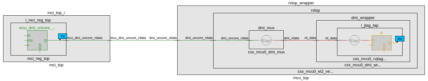
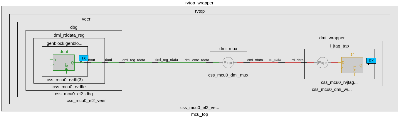
CDC analysis conclusions
- Missing synchronizers appear to be the result of “inferred” and/or only 2-FF instantiated synchronizers.
- dmi_jtag_to_core_sync.v contains inferred 2FF synchronizers on the control signals “dmi_reg_wr_en” and “dmi_reg_rd_en”.
- 2FF synchronizer inferences are considered non-compliant and should be replaced by an explicitly instantiated synchronization module, which is intended to be substituted on a per-integrator basis.
- cdc report scheme two_dff -severity violation
- Multi-bit signals are effectively pseudo-static and are qualified by synchronized control qualifiers.
- Pseudo-static: wr_data, wr_addr
- cdc signal reg_wr_data -module dmi_wrapper -stable
- cdc signal reg_wr_addr -module dmi_wrapper -stable
- Pseudo-static: wr_data, wr_addr
- The core clock frequency must be at least twice the TCK clock frequency of each TAP EPs for the JTAG data to pass correctly through the synchronizers.
CDC constraints
- cdc report scheme two_dff -severity violation
- cdc signal reg_wr_data -module dmi_wrapper -stable
- cdc signal reg_wr_addr -module dmi_wrapper -stable
- cdc signal rd_data -module dmi_wrapper -stable
- cdc signal reg_wr_data -module css_mcu0_dmi_wrapper -stable
- cdc signal reg_wr_addr -module css_mcu0_dmi_wrapper -stable
- cdc signal rd_data -module css_mcu0_dmi_wrapper -stable
- cdc signal jtag_dmi_req_i -module dmi_cdc -stable
- cdc signal jtag_dmi_resp_o -module dmi_cdc -stable
- cdc signal core_dmi_req_o -module dmi_cdc -stable
- cdc signal core_dmi_resp_i -module dmi_cdc -stable
Reset Domain Crossing
Reset Architecture
The below diagram illustrates the internal reset architecture of Caliptra SS.
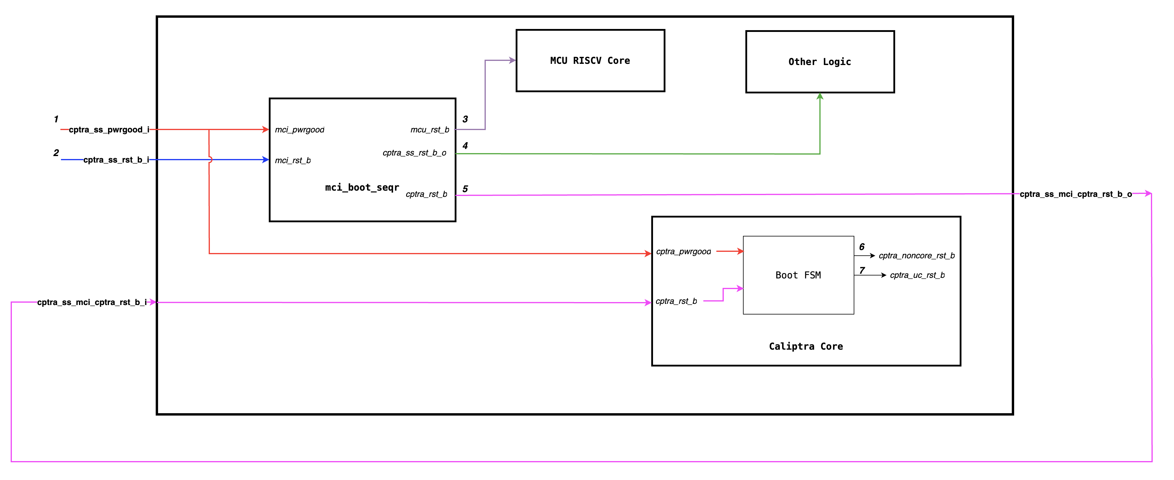
The reset block diagram below illustrates the RTL implemenation of various resets.
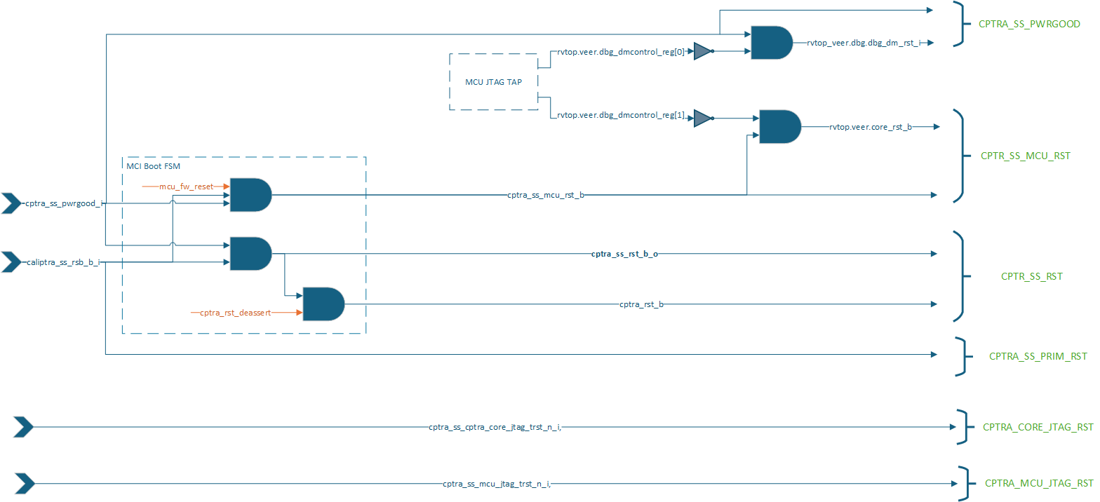
The below diagram illustrates how various internal blocks are connected to either primary resets or internally generated resets.
Similar to Caliptra Core, we solve the problem of RDC using gated clocks which are gated during reset assertion. Below diagram illustrates the clock connections of various sub-modules.
Reset Domain Stamping and Constraints
The Below table illustrates various reset domains that we have in the design. We assume that all resets are asserted at timestamp 5, and the constrained signal is held high or low around that time (for instance, from timestamp 2 to timestamp 8).
| Reset Group | Description | HW Reset Signal | Constraints | False path groups |
|---|---|---|---|---|
| CPTRA_SS_PWRGD | Primary reset input corresponding to SOC Powergood | cptra_ss_pwrgood_i | CPTRA_SS_PWRGD -> all | |
| CPTRA_SS_PRIM_RST | Primary reset input corresponding to SOC Warm Reset | cptra_ss_rst_b_i | caliptra_top_dut.soc_ifc_top1.soc_ifc_reg_hwif_out.CPTRA_FUSE_WR_DONE.done.value -> HIGH i3c.i3c.xrecovery_handler.xrecovery_executor.image_activated_o -> LOW i3c.i3c.xrecovery_handler.xrecovery_executor.payload_available_q -> LOW | CPTRA_SS_PRIM_RST -> CPTRA_CORE_UC_RST CPTRA_SS_PRIM_RST -> CPTRA_CORE_NON_CORE_RST CPTRA_SS_PRIM_RST -> CPTRA_SS_RST CPTRA_SS_PRIM_RST -> CPTRA_SS_MCU_RST |
| CPTRA_SS_RST | Caliptra SS MCI Boot Sequencer generated reset used by various other SS level logic blocks and Caliptra Core | cptra_ss_mci_cptra_rst_b_i mci_top_i.i_boot_seqr.cptra_ss_rst_b_o | mci_top_i.i_boot_seqr.rdc_clk_dis -> HIGH mci_top_i.i_boot_seqr.early_warm_reset_warn -> HIGH mci_top_i.i_boot_seqr.boot_fsm[3:0] = BOOT_IDLE i3c.i3c.xrecovery_handler.xrecovery_executor.image_activated_o -> LOW i3c.i3c.xrecovery_handler.xrecovery_executor.payload_available_q -> LOW caliptra_top_dut.soc_ifc_top1.soc_ifc_reg_hwif_out.CPTRA_FUSE_WR_DONE.done.value -> HIGH | CPTRA_SS_RST -> CPTRA_SS_PRIM_RST CPTRA_SS_RST -> CPTRA_CORE_NON_CORE_RST CPTRA_SS_RST -> CPTRA_CORE_UC_RST CPTRA_SS_RST -> CPTRA_SS_MCU_RST CPTRA_SS_RST -> CPTRA_DMI_NON_CORE_RST |
| CPTRA_CORE_NON_CORE_RST | Caliptra Core Boot FSM generated reset used by various other Caliptra Core logics | caliptra_top_dut.soc_ifc_top1.i_soc_ifc_boot_fsm.cptra_noncore_rst_b | caliptra_top_dut.soc_ifc_top1.i_soc_ifc_boot_fsm.rdc_clk_dis -> HIGH caliptra_top_dut.soc_ifc_top1.i_soc_ifc_boot_fsm.arc_IDLE -> HIGH mci_top_i.i_boot_seqr.rdc_clk_dis -> HIGH | CPTRA_CORE_NON_CORE_RST -> CPTRA_SS_RST CPTRA_CORE_NON_CORE_RST -> CPTRA_SS_PRIM_RST CPTRA_CORE_NON_CORE_RST -> CPTRA_CORE_UC_RST CPTRA_CORE_NON_CORE_RST -> CPTRA_SS_MCU_RST |
| CPTRA_CORE_UC_RST | Caliptra Core Boot FSM generated microcontroller reset for Caliptra Core RISCV | caliptra_top_dut.soc_ifc_top1.i_soc_ifc_boot_fsm.cptra_uc_rst_b | caliptra_top_dut.soc_ifc_top1.i_soc_ifc_boot_fsm.fw_update_rst_window -> HIGH caliptra_top_dut.aes_inst.aes_inst.u_aes_core.u_aes_control.gen_fsm[0].gen_fsm_p.u_aes_control_fsm_i.u_aes_control_fsm.aes_ctrl_cs[5:0] -> 6'b001001 caliptra_top_dut.sha3.hsel_i -> LOW caliptra_top_dut.aes_inst.aes_cif_req_dv -> LOW | |
| CPTRA_SS_MCU_RST | Caliptra SS MCI Boot Sequencer generated microcontroller reset for Caliptra SS RISCV | mci_top_i.i_boot_seqr.mcu_rst_b | mci_top_i.i_boot_seqr.fw_update_rst_window -> HIGH mci_top_i.i_mci_mcu_trace_buffer.mcu_trace_rv_i_valid_ip -> LOW |
The current analysis only focuses on RDC crossing which are internal to Caliptra SS. Any RDC crossings with external flops need to be handled by integrators.
Reset Sequencing
The below waveform illustrates how various resets of Caliptra SS and Caliptra Core are sequenced in the design.
The red and blue line indicates that the input Caliptra SS warm reset (cptra_ss_rst_b_i) needs to be asserted for atleast 32 clock cycles for the reset assertion to propagate through various levels of hierarhcy.
RDC Waivers
All Caliptra Core waivers are applicable at SS level as well. On top of those, we have the following waivers.
create_view_criteria \
    -name otp_broadcast_ss_rst_caliptra_core \
    -rule {E_RST_METASTABILITY} \
    -comment "waiver_for otp_broadcast related paths" \
    -criteria { ((ResetFlop =~ "*.u_caliptra_ss.u_otp_ctrl.otp_broadcast_o.secret_prod_partition_0_data.*")  ||  \
                 (ResetFlop =~ "*.u_caliptra_ss.u_otp_ctrl.otp_broadcast_o.valid*") ) &&  \
                 ((MetaStableFlop =~ "*.u_caliptra_ss.caliptra_top_dut.soc_ifc_top1.i_soc_ifc_reg.field_storage.fuse_field_entropy*") || \
                  (MetaStableFlop =~ "*.u_caliptra_ss.caliptra_top_dut.soc_ifc_top1.i_soc_ifc_reg.field_storage.fuse_uds_seed*") ) } \
    -replace
set_rule_status -use_view_criteria otp_broadcast_ss_rst_caliptra_core -status Waived -weakmatchfullgroup

create_view_criteria \
    -name path_ending_at_2ff_sync \
    -rule {E_RST_METASTABILITY} \
    -comment "wavier for 2ff sync" \
    -criteria { ((MetaStableFlop =~ "*.u_sync_1.gen_generic.u_impl_generic.*") || \
                  (MetaStableFlop =~ "*.i_rst_window_sync.*") ) } \
    -replace
set_rule_status -use_view_criteria path_ending_at_2ff_sync -status Waived -weakmatchfullgroup

create_view_criteria \
    -name no_axi_bus_active \
    -rule {E_RDC_METASTABILITY} \
    -comment "Before warm reset assertion, it is sure that is transaction pending on axi bus" \
    -criteria {  (ResetFlop      =~ "*.caliptra_top_dut.s_axi_active[2:0]") && \
                 (MetaStableFlop =~ "*cg.user_soc_ifc_icg.clk_slcg_0_generated_icg.p_clkgate.vudpi0.q")  } \
    -replace
set_rule_status -use_view_criteria no_axi_bus_active -status Waived -weakmatchfullgroup
Synthesis
Synthesis has been performed at CALIPTRA_SS_WRAPPER level which encompasses the following :-
- caliptra_ss_top
- Memories instantiated outside using tech specific macros
Design converges at 400MHz 0.72V using an industry standard, advanced technology node as of 2025 April.
Recommended LINT rules
A standardized set of lint rules is used to sign off on each release. The lint policy may be provided directly to integrators upon request to ensure lint is clean in the SoC.
Known Lint Issue
The following lint violations are known and expected in the current implementation:
Signal Width Mismatches
| Location | Description | Justification |
|---|---|---|
| mcu_mbox_csr.sv:271 | Signal width mismatch | MSB on RHS will be optimized out during synthesis |
Undriven signals
These are undriven signals and deemed to be OK. If exposed to SOC leave unconnected when integrating.
| Location | Signal | Justification |
|---|---|---|
el2_veer.sv | sb_axi_bready_ahb | Caliptra Core internal RV processor uses AHB, not AXI interface, so AXI is unconnected |
el2_veer.sv | ifu_axi_bready_ahb | Caliptra Core internal RV processor uses AHB, not AXI interface, so AXI is unconnected |
el2_veer.sv | lsu_axi_bready_ahb | Caliptra Core internal RV processor uses AHB, not AXI interface, so AXI is unconnected |
Terminology
| Abbreviation | Term | Description |
|---|---|---|
| AXI | Advanced eXtensible Interface | A high-performance, high-frequency communication protocol |
| I3C | Improved Inter-Integrated Circuit | A communication protocol for connecting sensors and other peripherals. |
| ECC | Error Correction Code | A method of detecting and correcting errors in data storage and transmission. |
| RISCV | Reduced Instruction Set Computer Five | An open standard instruction set architecture based on established RISC principles. |
| MCU | Manufacturer Control Unit | A small computer on a single integrated circuit containing a processor core, memory, and programmable input/output peripherals. |
| MCI | Manufacturer Control Interface (for MCU) | Manages the communication between the processor and the memory components. |
| FC | Fuse Controller | A one-time programmable memory controller used for storing critical configuration data and security keys. |
| LCC | Life Cycle Controller | Manages the different stages of the subsystem's lifecycle, including initialization, operation, and shutdown. |
84daa9a
| Index | Partition | Size [B] | Access Granule | Item | Byte Address | Size [B] |
|---|---|---|---|---|---|---|
| 0 | SW_TEST_UNLOCK_PARTITION | 72 | 32bit | CPTRA_SS_MANUF_DEBUG_UNLOCK_TOKEN | 0x000 | 64 |
| 64bit | SW_TEST_UNLOCK_PARTITION_DIGEST | 0x040 | 8 | |||
| 1 | SECRET_MANUF_PARTITION | 80 | 64bit | CPTRA_CORE_UDS_SEED | 0x048 | 64 |
| 64bit | SECRET_MANUF_PARTITION_DIGEST | 0x088 | 8 | |||
| 64bit | SECRET_MANUF_PARTITION_ZER | 0x090 | 8 | |||
| 2 | SECRET_PROD_PARTITION_0 | 24 | 64bit | CPTRA_CORE_FIELD_ENTROPY_0 | 0x098 | 8 |
| 64bit | SECRET_PROD_PARTITION_0_DIGEST | 0x0A0 | 8 | |||
| 64bit | SECRET_PROD_PARTITION_0_ZER | 0x0A8 | 8 | |||
| 3 | SECRET_PROD_PARTITION_1 | 24 | 64bit | CPTRA_CORE_FIELD_ENTROPY_1 | 0x0B0 | 8 |
| 64bit | SECRET_PROD_PARTITION_1_DIGEST | 0x0B8 | 8 | |||
| 64bit | SECRET_PROD_PARTITION_1_ZER | 0x0C0 | 8 | |||
| 4 | SECRET_PROD_PARTITION_2 | 24 | 64bit | CPTRA_CORE_FIELD_ENTROPY_2 | 0x0C8 | 8 |
| 64bit | SECRET_PROD_PARTITION_2_DIGEST | 0x0D0 | 8 | |||
| 64bit | SECRET_PROD_PARTITION_2_ZER | 0x0D8 | 8 | |||
| 5 | SECRET_PROD_PARTITION_3 | 24 | 64bit | CPTRA_CORE_FIELD_ENTROPY_3 | 0x0E0 | 8 |
| 64bit | SECRET_PROD_PARTITION_3_DIGEST | 0x0E8 | 8 | |||
| 64bit | SECRET_PROD_PARTITION_3_ZER | 0x0F0 | 8 | |||
| 6 | SW_MANUF_PARTITION | 520 | 32bit | CPTRA_CORE_ANTI_ROLLBACK_DISABLE | 0x0F8 | 4 |
| 32bit | CPTRA_CORE_IDEVID_CERT_IDEVID_ATTR | 0x0FC | 96 | |||
| 32bit | SOC_SPECIFIC_IDEVID_CERTIFICATE | 0x15C | 4 | |||
| 32bit | CPTRA_CORE_IDEVID_MANUF_HSM_IDENTIFIER | 0x160 | 16 | |||
| 32bit | CPTRA_CORE_SOC_STEPPING_ID | 0x170 | 4 | |||
| 32bit | CPTRA_SS_PROD_DEBUG_UNLOCK_PKS_0 | 0x174 | 48 | |||
| 32bit | CPTRA_SS_PROD_DEBUG_UNLOCK_PKS_1 | 0x1A4 | 48 | |||
| 32bit | CPTRA_SS_PROD_DEBUG_UNLOCK_PKS_2 | 0x1D4 | 48 | |||
| 32bit | CPTRA_SS_PROD_DEBUG_UNLOCK_PKS_3 | 0x204 | 48 | |||
| 32bit | CPTRA_SS_PROD_DEBUG_UNLOCK_PKS_4 | 0x234 | 48 | |||
| 32bit | CPTRA_SS_PROD_DEBUG_UNLOCK_PKS_5 | 0x264 | 48 | |||
| 32bit | CPTRA_SS_PROD_DEBUG_UNLOCK_PKS_6 | 0x294 | 48 | |||
| 32bit | CPTRA_SS_PROD_DEBUG_UNLOCK_PKS_7 | 0x2C4 | 48 | |||
| 64bit | SW_MANUF_PARTITION_DIGEST | 0x2F8 | 8 | |||
| 7 | SECRET_LC_TRANSITION_PARTITION | 184 | 64bit | CPTRA_SS_TEST_UNLOCK_TOKEN_1 | 0x300 | 16 |
| 64bit | CPTRA_SS_TEST_UNLOCK_TOKEN_2 | 0x310 | 16 | |||
| 64bit | CPTRA_SS_TEST_UNLOCK_TOKEN_3 | 0x320 | 16 | |||
| 64bit | CPTRA_SS_TEST_UNLOCK_TOKEN_4 | 0x330 | 16 | |||
| 64bit | CPTRA_SS_TEST_UNLOCK_TOKEN_5 | 0x340 | 16 | |||
| 64bit | CPTRA_SS_TEST_UNLOCK_TOKEN_6 | 0x350 | 16 | |||
| 64bit | CPTRA_SS_TEST_UNLOCK_TOKEN_7 | 0x360 | 16 | |||
| 64bit | CPTRA_SS_TEST_EXIT_TO_MANUF_TOKEN | 0x370 | 16 | |||
| 64bit | CPTRA_SS_MANUF_TO_PROD_TOKEN | 0x380 | 16 | |||
| 64bit | CPTRA_SS_PROD_TO_PROD_END_TOKEN | 0x390 | 16 | |||
| 64bit | CPTRA_SS_RMA_TOKEN | 0x3A0 | 16 | |||
| 64bit | SECRET_LC_TRANSITION_PARTITION_DIGEST | 0x3B0 | 8 | |||
| 8 | SVN_PARTITION | 40 | 32bit | CPTRA_CORE_FMC_KEY_MANIFEST_SVN | 0x3B8 | 4 |
| 32bit | CPTRA_CORE_RUNTIME_SVN | 0x3BC | 16 | |||
| 32bit | CPTRA_CORE_SOC_MANIFEST_SVN | 0x3CC | 16 | |||
| 32bit | CPTRA_CORE_SOC_MANIFEST_MAX_SVN | 0x3DC | 4 | |||
| 9 | VENDOR_TEST_PARTITION | 64 | 32bit | VENDOR_TEST | 0x3E0 | 32 |
| 64bit | VENDOR_TEST_PARTITION_DIGEST | 0x418 | 8 | |||
| 10 | VENDOR_HASHES_MANUF_PARTITION | 64 | 32bit | CPTRA_CORE_VENDOR_PK_HASH_0 | 0x420 | 48 |
| 32bit | CPTRA_CORE_PQC_KEY_TYPE_0 | 0x450 | 4 | |||
| 64bit | VENDOR_HASHES_MANUF_PARTITION_DIGEST | 0x458 | 8 | |||
| 11 | VENDOR_HASHES_PROD_PARTITION | 864 | 32bit | CPTRA_SS_OWNER_PK_HASH | 0x460 | 48 |
| 32bit | CPTRA_SS_OWNER_PQC_KEY_TYPE | 0x490 | 4 | |||
| 32bit | CPTRA_SS_OWNER_PK_HASH_VALID | 0x494 | 4 | |||
| 32bit | CPTRA_CORE_VENDOR_PK_HASH_1 | 0x498 | 48 | |||
| 32bit | CPTRA_CORE_PQC_KEY_TYPE_1 | 0x4C8 | 4 | |||
| 32bit | CPTRA_CORE_VENDOR_PK_HASH_2 | 0x4CC | 48 | |||
| 32bit | CPTRA_CORE_PQC_KEY_TYPE_2 | 0x4FC | 4 | |||
| 32bit | CPTRA_CORE_VENDOR_PK_HASH_3 | 0x500 | 48 | |||
| 32bit | CPTRA_CORE_PQC_KEY_TYPE_3 | 0x530 | 4 | |||
| 32bit | CPTRA_CORE_VENDOR_PK_HASH_4 | 0x534 | 48 | |||
| 32bit | CPTRA_CORE_PQC_KEY_TYPE_4 | 0x564 | 4 | |||
| 32bit | CPTRA_CORE_VENDOR_PK_HASH_5 | 0x568 | 48 | |||
| 32bit | CPTRA_CORE_PQC_KEY_TYPE_5 | 0x598 | 4 | |||
| 32bit | CPTRA_CORE_VENDOR_PK_HASH_6 | 0x59C | 48 | |||
| 32bit | CPTRA_CORE_PQC_KEY_TYPE_6 | 0x5CC | 4 | |||
| 32bit | CPTRA_CORE_VENDOR_PK_HASH_7 | 0x5D0 | 48 | |||
| 32bit | CPTRA_CORE_PQC_KEY_TYPE_7 | 0x600 | 4 | |||
| 32bit | CPTRA_CORE_VENDOR_PK_HASH_8 | 0x604 | 48 | |||
| 32bit | CPTRA_CORE_PQC_KEY_TYPE_8 | 0x634 | 4 | |||
| 32bit | CPTRA_CORE_VENDOR_PK_HASH_9 | 0x638 | 48 | |||
| 32bit | CPTRA_CORE_PQC_KEY_TYPE_9 | 0x668 | 4 | |||
| 32bit | CPTRA_CORE_VENDOR_PK_HASH_10 | 0x66C | 48 | |||
| 32bit | CPTRA_CORE_PQC_KEY_TYPE_10 | 0x69C | 4 | |||
| 32bit | CPTRA_CORE_VENDOR_PK_HASH_11 | 0x6A0 | 48 | |||
| 32bit | CPTRA_CORE_PQC_KEY_TYPE_11 | 0x6D0 | 4 | |||
| 32bit | CPTRA_CORE_VENDOR_PK_HASH_12 | 0x6D4 | 48 | |||
| 32bit | CPTRA_CORE_PQC_KEY_TYPE_12 | 0x704 | 4 | |||
| 32bit | CPTRA_CORE_VENDOR_PK_HASH_13 | 0x708 | 48 | |||
| 32bit | CPTRA_CORE_PQC_KEY_TYPE_13 | 0x738 | 4 | |||
| 32bit | CPTRA_CORE_VENDOR_PK_HASH_14 | 0x73C | 48 | |||
| 32bit | CPTRA_CORE_PQC_KEY_TYPE_14 | 0x76C | 4 | |||
| 32bit | CPTRA_CORE_VENDOR_PK_HASH_15 | 0x770 | 48 | |||
| 32bit | CPTRA_CORE_PQC_KEY_TYPE_15 | 0x7A0 | 4 | |||
| 32bit | CPTRA_CORE_VENDOR_PK_HASH_VALID | 0x7A4 | 16 | |||
| 64bit | VENDOR_HASHES_PROD_PARTITION_DIGEST | 0x7B8 | 8 | |||
| 12 | VENDOR_REVOCATIONS_PROD_PARTITION | 216 | 32bit | CPTRA_SS_OWNER_ECC_REVOCATION | 0x7C0 | 4 |
| 32bit | CPTRA_SS_OWNER_LMS_REVOCATION | 0x7C4 | 4 | |||
| 32bit | CPTRA_SS_OWNER_MLDSA_REVOCATION | 0x7C8 | 4 | |||
| 32bit | CPTRA_CORE_ECC_REVOCATION_0 | 0x7CC | 4 | |||
| 32bit | CPTRA_CORE_LMS_REVOCATION_0 | 0x7D0 | 4 | |||
| 32bit | CPTRA_CORE_MLDSA_REVOCATION_0 | 0x7D4 | 4 | |||
| 32bit | CPTRA_CORE_ECC_REVOCATION_1 | 0x7D8 | 4 | |||
| 32bit | CPTRA_CORE_LMS_REVOCATION_1 | 0x7DC | 4 | |||
| 32bit | CPTRA_CORE_MLDSA_REVOCATION_1 | 0x7E0 | 4 | |||
| 32bit | CPTRA_CORE_ECC_REVOCATION_2 | 0x7E4 | 4 | |||
| 32bit | CPTRA_CORE_LMS_REVOCATION_2 | 0x7E8 | 4 | |||
| 32bit | CPTRA_CORE_MLDSA_REVOCATION_2 | 0x7EC | 4 | |||
| 32bit | CPTRA_CORE_ECC_REVOCATION_3 | 0x7F0 | 4 | |||
| 32bit | CPTRA_CORE_LMS_REVOCATION_3 | 0x7F4 | 4 | |||
| 32bit | CPTRA_CORE_MLDSA_REVOCATION_3 | 0x7F8 | 4 | |||
| 32bit | CPTRA_CORE_ECC_REVOCATION_4 | 0x7FC | 4 | |||
| 32bit | CPTRA_CORE_LMS_REVOCATION_4 | 0x800 | 4 | |||
| 32bit | CPTRA_CORE_MLDSA_REVOCATION_4 | 0x804 | 4 | |||
| 32bit | CPTRA_CORE_ECC_REVOCATION_5 | 0x808 | 4 | |||
| 32bit | CPTRA_CORE_LMS_REVOCATION_5 | 0x80C | 4 | |||
| 32bit | CPTRA_CORE_MLDSA_REVOCATION_5 | 0x810 | 4 | |||
| 32bit | CPTRA_CORE_ECC_REVOCATION_6 | 0x814 | 4 | |||
| 32bit | CPTRA_CORE_LMS_REVOCATION_6 | 0x818 | 4 | |||
| 32bit | CPTRA_CORE_MLDSA_REVOCATION_6 | 0x81C | 4 | |||
| 32bit | CPTRA_CORE_ECC_REVOCATION_7 | 0x820 | 4 | |||
| 32bit | CPTRA_CORE_LMS_REVOCATION_7 | 0x824 | 4 | |||
| 32bit | CPTRA_CORE_MLDSA_REVOCATION_7 | 0x828 | 4 | |||
| 32bit | CPTRA_CORE_ECC_REVOCATION_8 | 0x82C | 4 | |||
| 32bit | CPTRA_CORE_LMS_REVOCATION_8 | 0x830 | 4 | |||
| 32bit | CPTRA_CORE_MLDSA_REVOCATION_8 | 0x834 | 4 | |||
| 32bit | CPTRA_CORE_ECC_REVOCATION_9 | 0x838 | 4 | |||
| 32bit | CPTRA_CORE_LMS_REVOCATION_9 | 0x83C | 4 | |||
| 32bit | CPTRA_CORE_MLDSA_REVOCATION_9 | 0x840 | 4 | |||
| 32bit | CPTRA_CORE_ECC_REVOCATION_10 | 0x844 | 4 | |||
| 32bit | CPTRA_CORE_LMS_REVOCATION_10 | 0x848 | 4 | |||
| 32bit | CPTRA_CORE_MLDSA_REVOCATION_10 | 0x84C | 4 | |||
| 32bit | CPTRA_CORE_ECC_REVOCATION_11 | 0x850 | 4 | |||
| 32bit | CPTRA_CORE_LMS_REVOCATION_11 | 0x854 | 4 | |||
| 32bit | CPTRA_CORE_MLDSA_REVOCATION_11 | 0x858 | 4 | |||
| 32bit | CPTRA_CORE_ECC_REVOCATION_12 | 0x85C | 4 | |||
| 32bit | CPTRA_CORE_LMS_REVOCATION_12 | 0x860 | 4 | |||
| 32bit | CPTRA_CORE_MLDSA_REVOCATION_12 | 0x864 | 4 | |||
| 32bit | CPTRA_CORE_ECC_REVOCATION_13 | 0x868 | 4 | |||
| 32bit | CPTRA_CORE_LMS_REVOCATION_13 | 0x86C | 4 | |||
| 32bit | CPTRA_CORE_MLDSA_REVOCATION_13 | 0x870 | 4 | |||
| 32bit | CPTRA_CORE_ECC_REVOCATION_14 | 0x874 | 4 | |||
| 32bit | CPTRA_CORE_LMS_REVOCATION_14 | 0x878 | 4 | |||
| 32bit | CPTRA_CORE_MLDSA_REVOCATION_14 | 0x87C | 4 | |||
| 32bit | CPTRA_CORE_ECC_REVOCATION_15 | 0x880 | 4 | |||
| 32bit | CPTRA_CORE_LMS_REVOCATION_15 | 0x884 | 4 | |||
| 32bit | CPTRA_CORE_MLDSA_REVOCATION_15 | 0x888 | 4 | |||
| 64bit | VENDOR_REVOCATIONS_PROD_PARTITION_DIGEST | 0x890 | 8 | |||
| 13 | VENDOR_SECRET_PROD_PARTITION | 528 | 64bit | CPTRA_SS_VENDOR_SPECIFIC_SECRET_FUSE_0 | 0x898 | 32 |
| 64bit | CPTRA_SS_VENDOR_SPECIFIC_SECRET_FUSE_1 | 0x8B8 | 32 | |||
| 64bit | CPTRA_SS_VENDOR_SPECIFIC_SECRET_FUSE_2 | 0x8D8 | 32 | |||
| 64bit | CPTRA_SS_VENDOR_SPECIFIC_SECRET_FUSE_3 | 0x8F8 | 32 | |||
| 64bit | CPTRA_SS_VENDOR_SPECIFIC_SECRET_FUSE_4 | 0x918 | 32 | |||
| 64bit | CPTRA_SS_VENDOR_SPECIFIC_SECRET_FUSE_5 | 0x938 | 32 | |||
| 64bit | CPTRA_SS_VENDOR_SPECIFIC_SECRET_FUSE_6 | 0x958 | 32 | |||
| 64bit | CPTRA_SS_VENDOR_SPECIFIC_SECRET_FUSE_7 | 0x978 | 32 | |||
| 64bit | CPTRA_SS_VENDOR_SPECIFIC_SECRET_FUSE_8 | 0x998 | 32 | |||
| 64bit | CPTRA_SS_VENDOR_SPECIFIC_SECRET_FUSE_9 | 0x9B8 | 32 | |||
| 64bit | CPTRA_SS_VENDOR_SPECIFIC_SECRET_FUSE_10 | 0x9D8 | 32 | |||
| 64bit | CPTRA_SS_VENDOR_SPECIFIC_SECRET_FUSE_11 | 0x9F8 | 32 | |||
| 64bit | CPTRA_SS_VENDOR_SPECIFIC_SECRET_FUSE_12 | 0xA18 | 32 | |||
| 64bit | CPTRA_SS_VENDOR_SPECIFIC_SECRET_FUSE_13 | 0xA38 | 32 | |||
| 64bit | CPTRA_SS_VENDOR_SPECIFIC_SECRET_FUSE_14 | 0xA58 | 32 | |||
| 64bit | CPTRA_SS_VENDOR_SPECIFIC_SECRET_FUSE_15 | 0xA78 | 32 | |||
| 64bit | VENDOR_SECRET_PROD_PARTITION_DIGEST | 0xA98 | 8 | |||
| 64bit | VENDOR_SECRET_PROD_PARTITION_ZER | 0xAA0 | 8 | |||
| 14 | VENDOR_NON_SECRET_PROD_PARTITION | 520 | 32bit | CPTRA_SS_VENDOR_SPECIFIC_NON_SECRET_FUSE_0 | 0xAA8 | 32 |
| 32bit | CPTRA_SS_VENDOR_SPECIFIC_NON_SECRET_FUSE_1 | 0xAC8 | 32 | |||
| 32bit | CPTRA_SS_VENDOR_SPECIFIC_NON_SECRET_FUSE_2 | 0xAE8 | 32 | |||
| 32bit | CPTRA_SS_VENDOR_SPECIFIC_NON_SECRET_FUSE_3 | 0xB08 | 32 | |||
| 32bit | CPTRA_SS_VENDOR_SPECIFIC_NON_SECRET_FUSE_4 | 0xB28 | 32 | |||
| 32bit | CPTRA_SS_VENDOR_SPECIFIC_NON_SECRET_FUSE_5 | 0xB48 | 32 | |||
| 32bit | CPTRA_SS_VENDOR_SPECIFIC_NON_SECRET_FUSE_6 | 0xB68 | 32 | |||
| 32bit | CPTRA_SS_VENDOR_SPECIFIC_NON_SECRET_FUSE_7 | 0xB88 | 32 | |||
| 32bit | CPTRA_SS_VENDOR_SPECIFIC_NON_SECRET_FUSE_8 | 0xBA8 | 32 | |||
| 32bit | CPTRA_SS_VENDOR_SPECIFIC_NON_SECRET_FUSE_9 | 0xBC8 | 32 | |||
| 32bit | CPTRA_SS_VENDOR_SPECIFIC_NON_SECRET_FUSE_10 | 0xBE8 | 32 | |||
| 32bit | CPTRA_SS_VENDOR_SPECIFIC_NON_SECRET_FUSE_11 | 0xC08 | 32 | |||
| 32bit | CPTRA_SS_VENDOR_SPECIFIC_NON_SECRET_FUSE_12 | 0xC28 | 32 | |||
| 32bit | CPTRA_SS_VENDOR_SPECIFIC_NON_SECRET_FUSE_13 | 0xC48 | 32 | |||
| 32bit | CPTRA_SS_VENDOR_SPECIFIC_NON_SECRET_FUSE_14 | 0xC68 | 32 | |||
| 32bit | CPTRA_SS_VENDOR_SPECIFIC_NON_SECRET_FUSE_15 | 0xC88 | 32 | |||
| 64bit | VENDOR_NON_SECRET_PROD_PARTITION_DIGEST | 0xCA8 | 8 | |||
| 15 | CPTRA_SS_LOCK_HEK_PROD_0 | 48 | 32bit | CPTRA_SS_LOCK_HEK_PROD_0_RATCHET_SEED | 0xCB0 | 32 |
| 64bit | CPTRA_SS_LOCK_HEK_PROD_0_DIGEST | 0xCD0 | 8 | |||
| 64bit | CPTRA_SS_LOCK_HEK_PROD_0_ZER | 0xCD8 | 8 | |||
| 16 | CPTRA_SS_LOCK_HEK_PROD_1 | 48 | 32bit | CPTRA_SS_LOCK_HEK_PROD_1_RATCHET_SEED | 0xCE0 | 32 |
| 64bit | CPTRA_SS_LOCK_HEK_PROD_1_DIGEST | 0xD00 | 8 | |||
| 64bit | CPTRA_SS_LOCK_HEK_PROD_1_ZER | 0xD08 | 8 | |||
| 17 | CPTRA_SS_LOCK_HEK_PROD_2 | 48 | 32bit | CPTRA_SS_LOCK_HEK_PROD_2_RATCHET_SEED | 0xD10 | 32 |
| 64bit | CPTRA_SS_LOCK_HEK_PROD_2_DIGEST | 0xD30 | 8 | |||
| 64bit | CPTRA_SS_LOCK_HEK_PROD_2_ZER | 0xD38 | 8 | |||
| 18 | CPTRA_SS_LOCK_HEK_PROD_3 | 48 | 32bit | CPTRA_SS_LOCK_HEK_PROD_3_RATCHET_SEED | 0xD40 | 32 |
| 64bit | CPTRA_SS_LOCK_HEK_PROD_3_DIGEST | 0xD60 | 8 | |||
| 64bit | CPTRA_SS_LOCK_HEK_PROD_3_ZER | 0xD68 | 8 | |||
| 19 | CPTRA_SS_LOCK_HEK_PROD_4 | 48 | 32bit | CPTRA_SS_LOCK_HEK_PROD_4_RATCHET_SEED | 0xD70 | 32 |
| 64bit | CPTRA_SS_LOCK_HEK_PROD_4_DIGEST | 0xD90 | 8 | |||
| 64bit | CPTRA_SS_LOCK_HEK_PROD_4_ZER | 0xD98 | 8 | |||
| 20 | CPTRA_SS_LOCK_HEK_PROD_5 | 48 | 32bit | CPTRA_SS_LOCK_HEK_PROD_5_RATCHET_SEED | 0xDA0 | 32 |
| 64bit | CPTRA_SS_LOCK_HEK_PROD_5_DIGEST | 0xDC0 | 8 | |||
| 64bit | CPTRA_SS_LOCK_HEK_PROD_5_ZER | 0xDC8 | 8 | |||
| 21 | CPTRA_SS_LOCK_HEK_PROD_6 | 48 | 32bit | CPTRA_SS_LOCK_HEK_PROD_6_RATCHET_SEED | 0xDD0 | 32 |
| 64bit | CPTRA_SS_LOCK_HEK_PROD_6_DIGEST | 0xDF0 | 8 | |||
| 64bit | CPTRA_SS_LOCK_HEK_PROD_6_ZER | 0xDF8 | 8 | |||
| 22 | CPTRA_SS_LOCK_HEK_PROD_7 | 48 | 32bit | CPTRA_SS_LOCK_HEK_PROD_7_RATCHET_SEED | 0xE00 | 32 |
| 64bit | CPTRA_SS_LOCK_HEK_PROD_7_DIGEST | 0xE20 | 8 | |||
| 64bit | CPTRA_SS_LOCK_HEK_PROD_7_ZER | 0xE28 | 8 | |||
| 23 | LIFE_CYCLE | 88 | 32bit | LC_TRANSITION_CNT | 0xE30 | 48 |
| 32bit | LC_STATE | 0xE60 | 40 |
Subsystem Registers
Redirecting to external documentation...
Click here if not redirected ↗
01b3839
Introduction
This document summarizes the current state of the I3C core developed by Antmicro for Caliptra within CHIPS Alliance.
The implementation follows the Errata 01 for MIPI I3C Basic Specification Version 1.1.1 dated 11.03.2022.
Documentation structure
This documentation comprises the following chapters:
- overview - summarizes the main notions of the project
- ccc - provides an overview of the CCCs implemented by the core
- phy - provides a description of the I3C PHY Layer logic
- error_handling - describes error detection, interrupt reporting, and recovery mechanisms
- firmware_guide - provides a firmware integration guide with bring-up flow and configuration requirements
- dv - describes verification tooling and testplans
- ext_cap - provides a description of Target Transaction Interface
- recovery_flow - describes the I3C-based Recovery mode workflow
- axi_id_filtering - provides information about the AXI transactions filtering feature
- axi_recovery_flow - describes the alternative, optional, recovery flow where the recovery data is transferred to the core over the AXI bus
- registers - provides auto-generated register descriptions
- known_limitations - provides information about known core limitations in specific releases
01b3839
I3C core overview
This chapter provides a high level overview of the I3C target functionalities implemented in the core.
Configuration script
The I3C Core is configured with the i3c_core_config Python script, which reads configurations from the i3c_core_configs.yaml YAML file.
The supported configurations can be found in the i3c_core_configs.yaml file.
More details on the usage of the tool can be found in the relevant README.
System Bus
The I3C core can connect to system buses via dedicated adapters:
- AXI4
- AHB - The AHB-Lite implementation is based on the AMBA 3 AHB-Lite Protocol Specification (IHI0033A)
Virtual target
The I3C core implements the Secure Firmware Recovery protocol according to the Open Compute "Secure Firmware Recovery" specification rev. 1.1-rc5.
For this purpose, the I3C core exposes a "virtual" target with its own static and dynamic bus addresses.
The virtual target implementation shares most of its logic with the "main" one while retaining a distinct data path.
Certain CCC commands like SETAASA and SETDASA are implemented separately for the "main" and "virtual" targets.
Register descriptions
Register descriptions are specified in the RDL format for I3C core CSRs:
- I3C Capability and Operational Registers (I3CBase)
- Programmable I/O (PIOControl)
- Extended Capabilities (I3C_EC)
- Device Address Table (DAT)
- Device Characteristic Table (DCT)
The RDL files generate the relevant SystemVerilog which can be found in the src/csr/ directory. The auto-generated descriptions are included in the Register descriptions chapter.
Target Interface Queues
There are also target interface queues via Target Transaction Interface (TTI):
- RX - read descriptor & data queues
- TX - write descriptor & data queues
- IBI - IBI combined descriptor + data queue
Target recovery interface
Several functionalities related to the recovery interface have been implemented for Caliptra:
-
Recovery mode enable control via a CSR field
-
Hardware recovery packet handling (private read/write)
-
Hardware PEC checksum calculation and checking
-
Access to Recovery CSRs from the I3C side
-
Status signaling via output pins:
recovery_payload_available_orecovery_image_activated_o
Address Behavior
Dynamic and Static Address Priority
Per the I3C specification, once a Target has been assigned a Dynamic Address (via ENTDAA, SETDASA, SETAASA, or SETNEWDA), it shall stop responding to its Static Address. The core implements this as follows:
- If
DYNAMIC_ADDR_VALID = 1, the Target matches only onDYNAMIC_ADDR - If
DYNAMIC_ADDR_VALID = 0andSTATIC_ADDR_VALID = 1, the Target matches onSTATIC_ADDR
This rule applies independently to both the main target and the virtual target.
IBI Address
When sending In-Band Interrupts, the Target uses a separate IBI address derived from the main (non-virtual) target's address with dynamic-over-static priority:
- If the Dynamic Address is valid, the IBI address is the Dynamic Address.
- Otherwise, the IBI address falls back to the Static Address.
This is implemented in configuration.sv:
assign target_ibi_addr_o = target_dyn_addr_valid_o ? target_dyn_addr_o : target_sta_addr_o;
assign target_ibi_addr_valid_o = target_sta_addr_valid_o || target_dyn_addr_valid_o;
IBI transmission is gated on target_ibi_addr_valid. If neither address is valid,
target_ibi_addr_valid is deasserted and any pending IBI requests are effectively masked
(the ibi_pending signal in i3c_target_fsm.sv requires target_ibi_addr_valid_i).
Virtual Target Addressing
The virtual target (used for recovery) has its own independent address pair
(VIRT_STATIC_ADDR, VIRT_DYNAMIC_ADDR) with the same dynamic-over-static priority rule.
Both the main and virtual target addresses are checked in parallel on every incoming
transaction. When the virtual target address matches, the virtual_device_sel signal
routes the data path to the recovery handler, and TTI queue interrupts are gated.
Private reads and writes
-
The core handles I3C private reads and writes
-
This functionality passes Avery test suite tests
-
Private writes push data to the TTI RX Queue, accessible from the AXI bus, allowing the CPU to read the data
- The number of received bytes is written into the TTI RX descriptor Queue
- The software is supposed to first read the descriptor data, and then the number of bytes defined by the descriptor for the TTI RX Queue
-
Private reads send data on I3C lines from TTI TX Queue
- The software has to write the TTI TX Queue prior to a I3C private read transaction
- The TTI TX descriptor is used similarly to set the max number of bytes to be sent in the next private read transaction
-
In-Band Interrupts (IBI)
The core is capable of raising In-Band Interrupts. IBIs are controlled using descriptors written to a dedicated IBI queue by software. Optional IBI data immediately follows the descriptor in the same queue.
The core watches the IBI queue for a descriptor write. Once a descriptor is written, the core peeks it and waits until the defined count of data words is written to the queue. Finally, the core outputs the Mandatory Data Byte (MDB) and the data as 8-bit words.
I3C Common Command Codes (CCC)
The I3C core supports all CCCs required by the I3C Basic spec. See ccc for the full list of supported CCCs, CCCs that update registers without firmware notification, and CCC error handling.
Other features
-
Target Reset Pattern is detected and causes assertion of output pins, based on the action selected with RSTACT:
peripheral_reset_oescalated_reset_o
-
The core correctly detects HDR-Exit Pattern
-
Optional 60 us HDR error recovery timer for TE0/TE1 error recovery (see error_handling)
-
Target error detection (TE0-TE5) with interrupt reporting and saturating counters (see error_handling)
01b3839
Physical Layer
This chapter provides a description of the I3C PHY Layer logic.
Common PHY Layer
The PHY is responsible for controlling external bus signals (SDA, SCL) and synchronizing them with an internal clock. It should also support bus arbitration. The I2C Core from the OpenTitan project can be used as a reference design for basic features of the PHY.
:::{figure-md} i3c_phy
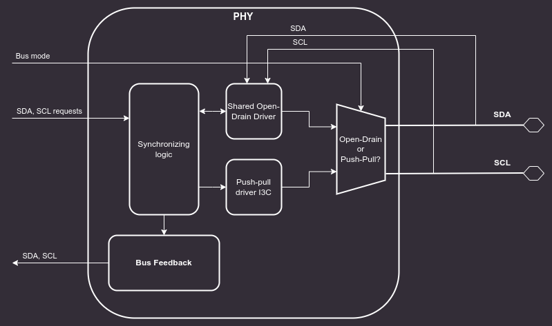
Block diagram of the I3C PHY Layer :::
SDA and SCL lines (5.1.3.1)
Both I2C and I3C datasheets specify that SDA and SCL lines should be bidirectional, connected to an active Open Drain class Pull-Up. Bus lines should be HIGH unless any device ties them to the GROUND.
:::{note}
In addition to the active Open Drain class Pull-Up, a High-Keeper is also required on the Bus.
The High-Keeper on the Bus should be strong enough to prevent system leakage from pulling SDA, and sometimes SCL, Low.
The High-Keeper on the Bus should also be weak enough for a Target with the minimum I{sub}OL PHY to be able to pull SDA, SCL, or both Low within the Minimum t{sub}DIG_L period.
The High-Keeper should be implemented during the physical design. PHY driver strength modeling will not be performed in this project. Base Controller will be delivered without the High-Keeper, however, it may become a configuration option later on. :::
Each bus line must be capable of switching between 4 logic states:
- No Pull-Up (High-Z)
- High-Keeper Pull-Up
- Open Drain Pull-Up
- Assert LOW
The OpenTitan I2C Core implements a Virtual Open Drain functionality which seems like a good solution for implementing the desired behavior on FPGA devices, while at the same time keeping it easy to use in silicon chips. Each bus line consists of 3 lines:
- Signal input (
scl_i,sda_i) - external input from the bus lines. - Signal output (
scl_o,sda_o) - internal signal, it is tied to the GROUND. - Signal output enable (
scl_en_o,sda_en_o) - internal signal enable, controlled by the core FSM.
This interface makes it easy to construct tri-state buffers.
The controller will never assert the external bus lines HIGH, since it is assumed that these lines are pulled up to V{sub}dd externally.
Switching from output to input is enough to achieve signals asserted HIGH.
Verilator does not natively support x and z states and their handling is explained in the official documentation.
Cocotb requires a wrapper to interact properly with an inout, which is described in Cocotb discussion #3506.
Considering these limitations, PHY is being tested functionally using Cocotb and tri-state logic.
Additionally, there is an RTL testbench run in Verilator and Icarus simulators that checks whether High-Z is set properly on I3C bus lines when the controller requests a high bus state.
Clock synchronization (5.1.7)
The entire core functions in a single clock domain - all I3C bus signals are sampled with this clock.
I3C timing configuration
The core implements 4 CSRs for controlling timings of the I3C bus:
T_F_REG- SCL falling timeT_R_REG- SCL rise timeT_HD_DAT_REG- SDA hold timeT_SU_DAT_REG- SDA setup time
In the target configuration, the first three should be set to 0, the T_SU_DAT_REG should be set according to the following equation:
reg_val = $floor(3 / system_clock_period) - 1
T_SU_DAT_REG = reg_val > 0 ? reg_val : 0
The core supports system clock frequencies above 333MHz, and SCL frequencies up to 12.5MHz. Below 333MHz Tsco I3C timing requirement of 12ns is not met. I3C specification defines Tsco as “Clock to Data Turnaround Time: The time duration between reception of an SCL edge and the start of driving an SDA change”. With 333MHz clock the maximum response time from the core is 12ns. This timing is not affected by the chip pads delays as per MIPI CSI I3C 1.1.1 specification.
The I3C core needs 3 system clock cycles between an event on a SCL line and driving the SDA. Since SCL and core clock are asynchronous, SCL can drop just after rising edge of the system clock. Such situation adds an additional clock cycle latency resulting in 4 cycles in total.
Maximal I3C core Tsco can be calculated with the Tsco = 4 * Tsys_clk formula , where Tsys_clk is a system clock period.
The minimum frequency calculation (333MHz) accounts only for the
I3C core internal logic delay. It does **not** include timing delays
introduced to and from the PADs. Integrators must account for these additional
delays when selecting the system clock frequency.
Future core releases will enable the GETMXDS CCC support allowing the core to advertise longer Tsco times for lower system clock frequencies.
SDA Output Path and Output Enable
The SDA output path uses a dedicated output enable (sda_oe) signal in addition to the
data value (sda_o). The bus_tx_flow module computes both based on the drive mode
(Open Drain or Push-Pull) and the data value being transmitted:
sda_oe = drive_mode_is_pushpull OR (NOT data_msb)
The resulting truth table for the SDA pad:
| sel_od_pp | sda_o | sda_oe | IO State |
|---|---|---|---|
| 0 (OD) | 0 | 1 | Drive Low |
| 0 (OD) | 1 | 0 | High-Z (released) |
| 1 (PP) | 0 | 1 | Drive Low |
| 1 (PP) | 1 | 1 | Drive High |
In Open Drain mode, the pad is released (High-Z) when driving a logical 1, allowing the external pull-up to assert the line. In Push-Pull mode, the pad actively drives both high and low.
The PHY module (i3c_phy.sv) passes these signals through to the pad interface:
ctrl_sda_oe_i->ctrl_sda_oe_o(output enable passthrough)sel_od_pp_i->sel_od_pp_o(drive mode passthrough)
I/O Signal Routing Constraints
All six I3C bus I/O signals (scl_i, sda_i, scl_o, sda_o, scl_oe, sda_oe)
must be routed together in physical design. The two-flop synchronizers
(scl_synchronizer, sda_synchronizer) and the output-path flops should be placed
close to the I/O pads to minimize routing skew between input and output paths.
Keeping the synchronizing flops and output flops near each other and near the pads ensures that:
- Input sampling latency is minimized and consistent across SCL and SDA.
- Output drive timing (t{sub}
SCO) is not degraded by long internal routing. - Skew between
sda_o/sda_oeand the correspondingsda_isample point remains within the timing budget described in the I3C timing configuration section above.
The `sel_od_pp_o` (Open Drain / Push-Pull select) signal should also be routed
alongside `sda_o` and `sda_oe` since it directly controls the pad driver mode
and must be stable before the pad switches drive state.
01b3839
Design verification
This chapter presents the available models and tools which are used for I3C verification. The core is verified with the Cocotb + unit tests and the UVM test suite.
This section contains testplans for the verification.
Definitions:
testplan- an organized collection of testpointstestpoint- an actionable item, which can be turned into a test:name- typically related to the tested featuredesc- detailed description; should contain description of the feature, configuration mode, stimuli, expected behavior.stage- can be used to assign testpoints to milestones.tests- names of implemented tests, which cover the testpoint. Relation test-testpoint can be many to many.tags- additional tags that can be used to group testpoints
Full overview of tests can be found in Testplan summary{.external}.
Testplans for individual blocks
:heading-offset: 2
Testplans for the core
:heading-offset: 2
Compliance test suite
The list of non-public tests which utilize Avery I3C VIP framework and have been successfully ran against the design is available in the CTS list.
01b3839
Specification for I3C Vendor-Specific Extended Capabilities
This chapter provides a description of Target Transaction Interface that created for the Standby Controller according to the normative specification of the Vendor-Specific Extended Capabilities for the I3C Controller as per section 7.7.13 of the {term}I3C HCI spec.
Security
The HCI specification defines Extended Capabilities as a list of linked lists, which can be discovered from software through a series of CSR reads. This mechanism is unacceptable for the Recovery Mode as memory offsets must be known at synthesis time. Implementation based on this specification should provide a list of known memory offsets for each of the Extended Capabilities.
:::{note} In order to increase security of the solution, the offsets are provided, so software may choose to skip the discovery mechanism. This specification is compliant with the original specification, so the mechanism of discovery can still be used, if needed. :::
Extended Capabilities
Standby Controller Mode - 0x12
The Standby Controller Mode follows the {term}I3C HCI spec:
- Chapter 6 Theory of Operation
- Section 6.17 Standby Controller Mode
- Chapter 7 Register Interface
- Section 7.7.11 Standby Controller Mode
Vendor-specific Extended Capabilities
This specification provides definitions and descriptions of the following Capabilities:
- Controller Config
- Standby Controller Mode
- Secure Firmware Recovery Interface
- Target Transaction Interface
- SoC Management Interface
:::{list-table} Extended capabilities registers :name: tab-capabilities-registers :widths: 60 20 20
-
- Extended Capability
- ID
- Memory Offset
-
- Controller Config
- 0x02
- Implementer
-
- Standby Controller Mode
- 0x12
- Implementer
-
- Secure Firmware Recovery Interface
- 0xC0
- Implementer
-
- SoC Management Interface
- 0xC1
- Implementer
-
- Target Transaction Interface
- 0xC4
- Implementer :::
Controller Config - 0x02
The Controller Config Capability follows section 7.7.3 of the {term}I3C HCI spec.
Secure Firmware Recovery Interface - 0xC0
This section is based on the Open Compute Project Secure Firmware Recovery, Version 1.1-rc5 and the I3C Target Recovery Specification.
The EXTCAP_HEADER is located at the SEC_FW_RECOVERY_OFFSET memory offset.
The registers are aligned to DWORD size (4 bytes), unless specified otherwise.
:::{list-table} Secure Firmware Recovery Interface :name: tab-secure-firmware-recovery-interface :widths: 40 60
-
- Register Name
- Role
-
- EXTCAP_HEADER
- Information about the Extended Capability
-
- PROT_CAP_0
- Device Capabilities Information
-
- PROT_CAP_1
- Device Capabilities Information
-
- PROT_CAP_2
- Device Capabilities Information
-
- PROT_CAP_3
- Device Capabilities Information
-
- DEVICE_ID_0
- Device identity information
-
- DEVICE_ID_1
- Device identity information
-
- DEVICE_ID_2
- Device identity information
-
- DEVICE_ID_3
- Device identity information
-
- DEVICE_ID_4
- Device identity information
-
- DEVICE_ID_5
- Device identity information
-
- DEVICE_ID_6
- Device identity information
-
- DEVICE_STATUS_0
- Device status information
-
- DEVICE_STATUS_1
- Device status information
-
- DEVICE_RESET
- Device reset and control
-
- RECOVERY_CTRL
- Recovery control and image activation
-
- RECOVERY_STATUS
- Recovery status information
-
- HW_STATUS
- Hardware status including temperature
-
- INDIRECT_FIFO_CTRL_0
- Indirect FIFO memory window control
-
- INDIRECT_FIFO_CTRL_1
- Indirect FIFO memory window control
-
- INDIRECT_FIFO_STATUS_0
- Indirect FIFO memory window status
-
- INDIRECT_FIFO_STATUS_1
- Indirect FIFO memory window status
-
- INDIRECT_FIFO_STATUS_2
- Indirect FIFO memory window status
-
- INDIRECT_FIFO_STATUS_3
- Indirect FIFO memory window status
-
- INDIRECT_FIFO_STATUS_4
- Indirect FIFO memory window status
-
- INDIRECT_FIFO_STATUS_5
- Indirect FIFO memory window status
-
- INDIRECT_FIFO_DATA
- Indirect FIFO memory window for pushing recovery image :::
SoC Management Interface - 0xC1
The SoC Management Interface is provided to enable additional configuration capabilities to the system integrator, e.g. programability of PHY Devices.
The SOC_MGMT_EXTCAP_HEADER is located at the SOC_MGMT_SECTION_OFFSET memory offset.
The registers are aligned to DWORD size (4 bytes), unless specified otherwise.
:::{list-table} SoC Management Interface :name: tab-soc-management-interface :widths: 50 50
-
- Register Name
- Role
-
- SOC_MGMT_EXTCAP_HEADER
- Information about the Extended Capability
-
- SOC_MGMT_CONTROL
- TBD
-
- SOC_MGMT_STATUS
- TBD
-
- SOC_MGMT_RSVD_0
- TBD
-
- SOC_MGMT_RSVD_1
- TBD
-
- SOC_MGMT_RSVD_2
- TBD
-
- SOC_MGMT_RSVD_3
- TBD
-
- SOC_MGMT_FEATURE_0
- TBD
-
- SOC_MGMT_FEATURE_1
- TBD
-
- SOC_MGMT_FEATURE_2
- TBD
-
- SOC_MGMT_FEATURE_3
- TBD
-
- …
- TBD
-
- SOC_MGMT_FEATURE_15
- TBD :::
Details of the operation are implementation specific. It is permissible to implement all registers as generic RW registers.
Target Transaction Interface - 0xC4
The Target Transaction Interface (TTI) provides additional registers and queues to enable data flow for Devices configured in the Target Mode.
This specification is meant for Standby Controllers which are capable of operating in Target Mode, therefore implementations are required to advertise the TTI by setting the Target_XACT_SUPPORT field of STBY_CR_CAPABILITIES.
:::{note} The term "TX" is used to denote instances in which the software performs a write to respond to an I3C Bus Read transaction. :::
:::{note} The term "RX" is used to denote instances in which the software performs a read to respond to an I3C Bus Write transaction :::
Operation
TTI is used to handle generic Read-Type and Write-Type transactions sent by the Standby Controller on the I3C bus. In this mode, software is responsible for servicing TX and RX queues based on the interrupt signals.
There are 5 queues to communicate between the bus and the register interface:
- TTI TX Descriptor queue, which holds information about read transfer
- TTI TX Data queue to buffer data written from the Target Device to the bus
- TTI RX Descriptor queue, which holds information about write transfer
- TTI RX Data queue to buffer data read from the bus by the Target Device
- TTI IBI queue to buffer data which will be written to the Bus as an In-Band Interrupt
Bus Read Transaction
After the Bus Read Transaction is acknowledged by the Target Device, it performs a write to the Interrupt Register to inform software of a pending read transaction. Software writes the response data to the TX queue and the TX descriptor to the TTI TX Descriptor queue.
Bus Write Transaction
The Bus Write Transaction is acknowledged by the Device if the transaction address matches the Device address and the RnW bit is set to 0.
The Target Device writes incoming bytes to the TTI RX Data Queue.
After the transaction ends, a TTI RX Descriptor is generated and pushed to the TTI RX Descriptor Queue for the software access.
Then, interrupt RX_DESC_STAT is raised.
:::{figure-md} fig-ext-cap-pwrite-timing
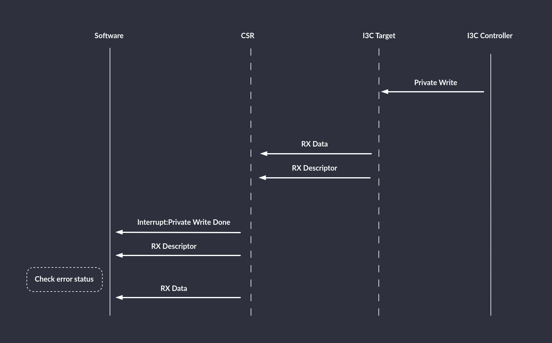
Private Write timing diagram :::
During the Private Write transaction, an error can be caused by:
- bit flip, which will be detected by the parity bit
- lack of space in the RX queue (overrun)
:::{figure-md} fig-ext-cap-pwrite-overrun
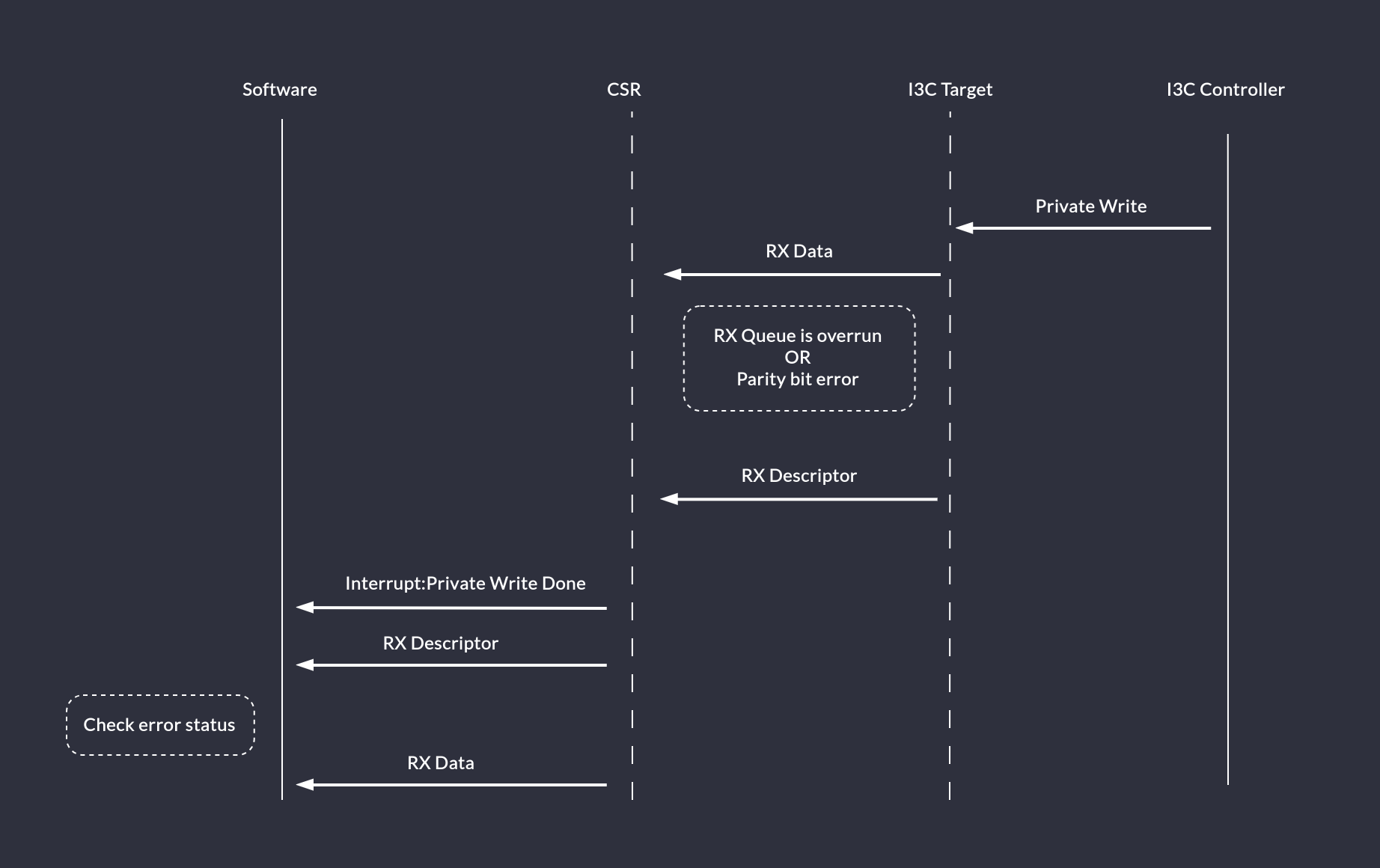
Private Write timing diagram: Parity bit error or RX Queue overrun scenario :::
If an Controller writes more data to the Target Device than it is capable to handle (even with triggering interrupts on threshold), the generated TTI RX Descriptor will indicate an error status and the Target Device should not ACK data on the bus.
The Controller can attempt mitigating such a situation by reading Target queue size from the TTI_QUEUE_SIZE register before sending a big chunk of data.
In-Band Interrupts
The Controller expects to receive an IBI Status Descriptor which is then followed by consecutive DWORDs of IBI Data.
:::{figure-md} fig-ext-cap-ibi
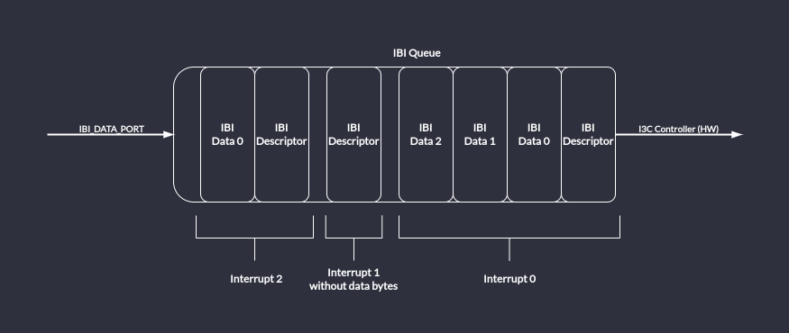
IBI Queue: partially filled with 3 interrupts. :::
In order to request an IBI, first the software should read the IBI queue size and set the queue threshold accordingly. Next, the interrupts should be enabled and an IBI descriptor with data can be written to the IBI_DATA_PORT. If, at this time, the IBI_THLD_STAT bit is set, then software should not attempt to write another IBI Descriptor into the queue. Software should wait until the IBI_THLD_STAT is cleared by hardware. The Target device will not try to send the IBI onto the I3C Bus until the bus is in the Available state. Also, it will read the IBI descriptor and wait until the IBI queue has all required data entries*. After meeting these conditions, the IBI will be driven onto the bus. The Target device will raise the IBI_DONE interrupt to notify that the IBI is finished. The software should read the LAST_IBI_STATUS to determine if the IBI ended successfully or was rejected. In case of failure, if the data integrity was not violated, the IBI will be retried once automatically.
:::{figure-md} fig-ext-cap-ibi-timing
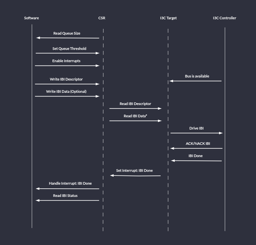
IBI Timing Diagram: send an IBI. :::
Register Interface
For a detailed list of TTI registers, refer to the TTI Registers chapter.
Data Structures (descriptors)
The TX Descriptor is 32-bit wide and has the following format:
:::{list-table} Target Transaction Interface TX Descriptor Format :name: tab-tti-target-transaction-interface-tx-descriptor :widths: 30 30 40
-
- Field Name
- Position (Size [bits])
- Description
-
- DATA_LENGTH
- [15:0] (16)
- Number of data bytes in the TX Transaction. :::
The RX Descriptor is 32-bit wide and has the following format:
:::{list-table} Target Transaction Interface RX Descriptor Format :name: tab-tti-target-transaction-interface-rx-descriptor :widths: 30 30 40
-
- Field Name
- Position (Size [bits])
- Description
-
-
ERROR
-
[31:28] (4)
-
Error occurred during this transaction. Software should read and discard data from the RX Queue.
Values:
0x0: Success
0x1: Generic error
0x2-0xF: Reserved, will be used to determine type of error.
-
-
- DATA_LENGTH
- [15:0] (16)
- Number of data bytes in the RX Transaction. :::
The IBI Descriptor is 32-bit wide and has the following format:
:::{list-table} Target Transaction Interface IBI Descriptor Format :name: tab-tti-target-transaction-interface-ibi-descriptor :widths: 30 30 40
-
- Field Name
- Position (Size [bits])
- Description
-
- MDB
- [31:24] (8)
- Mandatory Data Byte. This field is valid if BCR[2] is set.
-
- DATA_LENGTH
- [7:0] (8)
- Number of data bytes in the IBI. :::
TTI Queues
TTI TX Descriptor, TTI TX Data, TTI RX Descriptor, TTI RX Data and TTI IBI queues are implemented as FIFO queues of 32 bit (1 DWORD) width.
Depth should be parametrizable and the TTI_QUEUE_SIZE register’s reset value should be set accordingly.
In order to prevent overflow/underrun scenarios, a programmable threshold signal is provided.
Software-issued reset of the queues contents is also possible.
01b3839
Recovery flow
The recovery flow is implemented according to the Open Compute Secure Firmware Recovery standard v1.1-rc5. The recovery mode is handled through the virtual I3C target implemented by the core. In the Recovery Mode the Recovery Initiator Device (e.g. BMC) is primarily responsible for streaming the Firmware Recovery Image to the I3C Core. In order to facilitate this process, the I3C Core implements CSRs as specified in the Secure Firmware Recovery Interface. The firmware is responsible for implementing the recovery flow and transferring firmware data to the program memory.
For the alternative AXI-based recovery flow, see [axi_recovery_flow](axi_recovery_flow.md).
Recovery Flow Actors
| Actor | Interface | Role |
|---|---|---|
| Recovery Initiator | I3C bus (virtual target addr) | BMC or Controller that sends firmware image |
| I3C Core | Recovery Handler HW | Translates I3C commands to recovery CSR accesses |
| Device Firmware | AXI bus | Reads FIFO data, manages recovery state, boots image |
Recovery Flow Timeline
The diagram below shows the interleaved operations between the three actors. All CSR accesses from the Recovery Initiator use I3C private transfers to the virtual target address. Device Firmware accesses CSRs over the AXI bus.
Recovery Initiator I3C Core (Recovery CSRs) Device Firmware
(I3C Bus) ------------------------ ---------------
| | |
| | 1. Configure I3C core
| | Set PROT_CAP bits:
| | bit 0 (DEVICE_ID)
| | bit 4 (DEVICE_STATUS)
| | bit 5 (INDIRECT_CTRL)
| | bit 7 (Push C-image)
| | |
| | 2. Write DEVICE_STATUS
| | .DEV_STATUS = 0x3
| | (enter recovery mode)
| | |
| | 3. Write RECOVERY_STATUS
| | .DEV_REC_STATUS = 0x1
| | .REC_IMG_INDEX = <stage>
| | (awaiting image)
| | |
| | 3a. Wait for payload_available_o
| | to deassert (no-op on first
| | stage; on subsequent stages
| | waits for Initiator to complete
| | prior image handshake; in AXI
| | bypass mode waits for Image
| | Provider to clear
| | REC_PAYLOAD_DONE at step 17)
| | |
4. Read PROT_CAP | |
(verify recovery caps) | |
| | |
5. Read DEVICE_ID | |
(identify device) | |
| | |
6. Poll DEVICE_STATUS | |
until DEV_STATUS == 0x3 | |
| | |
7. Read RECOVERY_STATUS | |
confirm DEV_REC_STATUS == 0x1 | |
| | |
8. Write RECOVERY_CTRL | |
.CMS = 0, .REC_IMG_SEL = 0x1 | |
| | |
9. Write INDIRECT_FIFO_CTRL | |
.RESET = 1 (reset FIFO) | |
.IMAGE_SIZE = size in 4B units | |
| | |
v | |
,----------------------------. | |
| 10. DATA TRANSFER LOOP | | |
| (Initiator writes, | | |
| FW reads) | | |
`----------------------------' | |
| | |
| I3C Write INDIRECT_FIFO ----->| INDIRECT_FIFO |
| _DATA (chunk + PEC) | | |
| | `-----> Read by |
| | Device FW |
| | |
| I3C NACKs when FIFO full | DMA triggered by |
| (flow control via NACK) | payload_available_o |
| | (reads FIFO_SIZE or |
| | remaining bytes) |
| | |
| ... repeat until all data transferred ... |
| | |
| | 11. Write DEVICE_STATUS
| | .DEV_STATUS = 0x4
| | (recovery pending)
| | |
| | 12. Poll RECOVERY_CTRL
| | .ACTIVATE_REC_IMG
| | until == 0xF
| | |
13. Write RECOVERY_CTRL | |
.ACTIVATE_REC_IMG = 0xF | |
| | |
| | 14. Write DEV_REC_STATUS = 0x2
| | (processing image)
| | |
15. Poll DEVICE_STATUS.DEV_STATUS | |
Wait while DEV_STATUS == 0x4 | |
(Device FW is validating the image) | |
| | |
| | 16. Validate image
| | (crypto verification)
| | |
| | [Intermediate, on success]
| | Reset INDIRECT_FIFO_CTRL
| | -> loop back to step 2
| | (with next REC_IMG_INDEX)
| | |
| | [On error (any stage)]
| | Write DEV_REC_STATUS >= 0xc
| | Write DEV_STATUS = 0xF
| | |
| | [Final stage, on success]
| | Write DEV_REC_STATUS = 0x3
| | Write DEV_STATUS = 0x1
| | (recovery successful,
| | device healthy)
| | |
17. DEV_STATUS changed from 0x4: | |
0x3 = next stage ready | |
-> go back to step 6 | |
0x1 = recovery complete | |
-> exit | |
0xF = error | |
-> abort recovery | |
| | |
Key Differences from AXI Bypass Flow
The Device Firmware side of the flow is identical regardless of transport. The only differences are on the data provider (Initiator / Image Provider) side:
| Aspect | I3C Recovery Flow | AXI Bypass Flow |
|---|---|---|
| Data path | I3C bus to virtual target | AXI bus direct to FIFO |
| Initiator | External BMC/Controller | Internal Image Provider |
| PEC checksum | Required on every I3C transfer | Not used |
| FIFO full handling | I3C core NACKs the write | Image Provider polls FIFO status |
| CSR access | I3C private write/read commands | Direct AXI register access |
| Activation | Initiator writes RECOVERY_CTRL directly | Image Provider writes via W1C register |
REC_PAYLOAD_DONE | Not used (HW manages payload_available_o) | Image Provider sets/clears to signal last chunk |
**Inter-stage synchronization**: In multi-image recovery flows, Device
Firmware must wait for `payload_available_o` to deassert after writing
`RECOVERY_STATUS` (step 3) and before polling for new payload. In AXI
bypass mode, `payload_available_o` can remain asserted between stages
because the Image Provider's `REC_PAYLOAD_DONE` from the prior stage is
still set. The Image Provider clears `REC_PAYLOAD_DONE` when it enters
the next stage (step 17 in the AXI bypass flow). Without this wait,
Device Firmware may read stale `IMAGE_SIZE` from the prior stage and
set up DMA transfers with the wrong byte count.
Register Reference
Recovery registers are part of the Secure Firmware Recovery Interface
extended capability. See {ref}tab-secure-firmware-recovery-interface in
ext_cap for the full register list and field descriptions.
Recovery handler
Since the OCP Secure Firmware Recovery standard describes a set of CSRs that are the interface between the device being updated and the Recovery Initiator, I3C transactions that access them must be handled in the logic instead of the firmware, which is the purpose of the Recovery Handler block.
When the recovery mode is active, the handler takes over the TTI interface of the controller.
:::{figure-md} recovery_handler
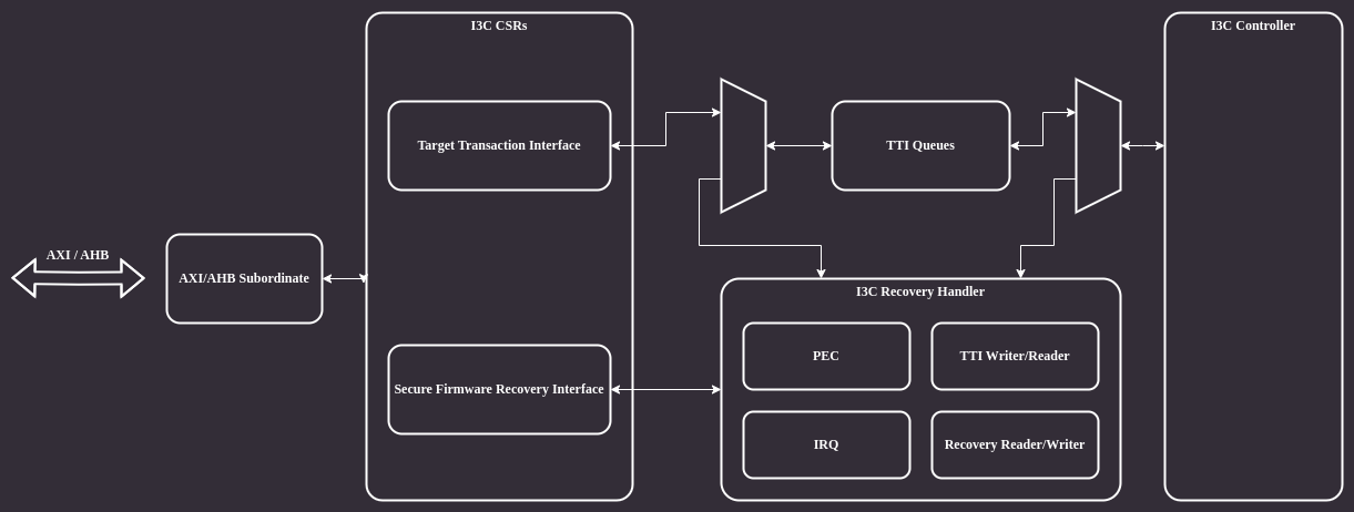
Recovery handler :::
The architecture of the Recovery Handler module is shown in the block diagram below:
:::{figure-md} recovery_handler_bd
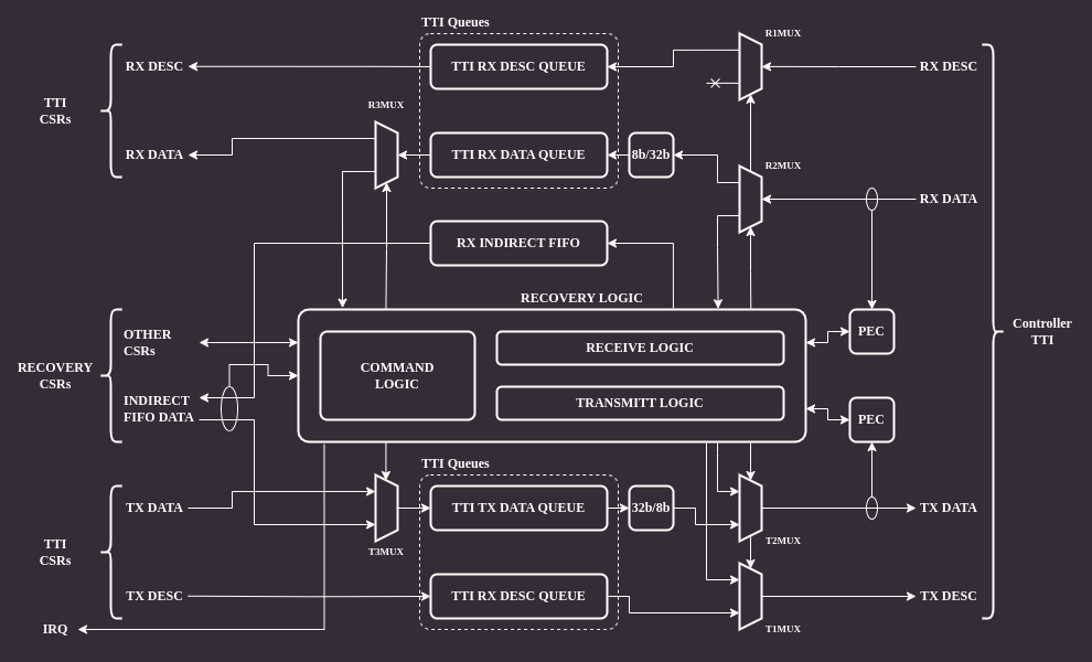
Recovery handler architecture :::
The module's backend is connected directly to the controller's TTI interface.
There are several muxes on the RX and TX data paths which allow bypassing the module in normal operation mode and remove/inject data in recovery mode.
There are two PEC (Packet Error Code) blocks responsible for calculating CRC for RX and TX data paths.
The CRC algorithm operates on individual bytes and implements C(x) = x^8+x^2+x^1+1 polynomial (see MCTP I3C binding, section 5.3.1).
The frontend is connected to I3C core CSRs accessible by software.
Normal operation
When the recovery mode is disabled the core allows accessing only a subset of recovery mode CSRs over I3C on the virtual target address. These are the registers marked as "available anytime" by the recovery interface specification. An attempt to access other CSRs results in a NACK response.
Recovery operation
When the recovery mode is enabled all recovery CSRs can be accessible via I3C bus. Accesses to the registers must be performed via the virtual target address.
CSR access via I3C
Recovery mode CSRs are accessible through the I3C bus. The following protocol is used to implement read/write operations:
CSR write
:::{figure-md} csr_write
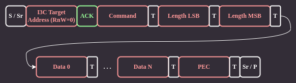
CSR write :::
The Recovery Initiator sends a command byte, followed by 16-bit payload length LSB and MSB bytes using I3C private transfers. The payload data immediately follows the length bytes. Each transfer ends with an additional byte containing a Packet Error Code (PEC) checksum.
CSR read
:::{figure-md} csr_read
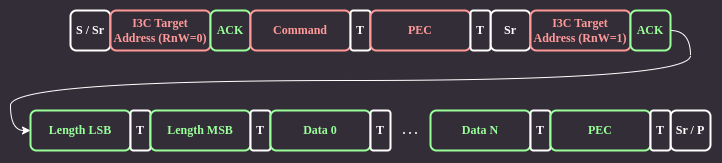
CSR read :::
For CSR read, the Recovery Initiator sends only the command byte and PEC checksum. Next, it issues a repeated start and begins a private read transaction. The device responds by sending data length LSB and MSB bytes, followed by the data and PEC.
Recovery handler operation
The main job of the Recovery Handler is providing hardware means for an active controller to access CSRs relevant to the recovery operation.
CSR write
When the Recovery Initiator writes to a CSR through I3C, the handler receives
the command byte, two length bytes, payload data, and a trailing PEC byte. The
PEC is computed over CMD + LEN + DATA using CRC-8. The handler validates the
transaction in CmdDispatch after all bytes are received.
The following errors are detected:
- CRC/PEC error: computed PEC does not match received PEC byte
- Length error: payload length does not match expected CSR size, premature Stop/Restart, or FIFO overflow
- Unsupported command error: invalid command code, or access to a recovery-only CSR when recovery mode is not active
- Read-only error: write attempt to a read-only CSR (reported as unsupported command per OCP spec)
- Bus-level parity error: T-bit parity error detected on the I3C bus during PEC or length bytes (reported as CRC error)
On any error, the handler enters an Error state that drains remaining bus
bytes, discards all received data, and writes the
error code to DEVICE_STATUS_0.PROTOCOL_ERROR. The CSR is not updated.
PEC errors are also reported through the TTI error interrupt path. All recovery handler errors have dedicated interrupt status bits, enable bits, detection enables, and saturating counters:
| Error | Interrupt Status | Detection Enable | Counter |
|---|---|---|---|
| CRC/PEC | RI_PEC_ERR_STAT | RI_PEC_ERR_DET_EN | TARGET_ERR_CNT_RI_PEC |
| Length | RI_LENGTH_ERR_STAT | RI_LENGTH_ERR_DET_EN | TARGET_ERR_CNT_RI_LENGTH |
| Read-only | RI_READONLY_ERR_STAT | RI_READONLY_ERR_DET_EN | TARGET_ERR_CNT_RI_READONLY |
| Unsupported | RI_UNSUPPORTED_ERR_STAT | RI_UNSUPPORTED_ERR_DET_EN | TARGET_ERR_CNT_RI_UNSUPPORTED |
| RX FIFO overflow | RI_RX_FIFO_OVERFLOW_ERR_STAT | RI_RX_FIFO_OVERFLOW_ERR_DET_EN | TARGET_ERR_CNT_RI_RX_FIFO_OVERFLOW |
| Indirect FIFO overflow | RI_INDIRECT_FIFO_OVERFLOW_ERR_STAT | RI_INDIRECT_FIFO_OVERFLOW_ERR_DET_EN | TARGET_ERR_CNT_RI_INDIRECT_FIFO_OVERFLOW |
All registers are in the TARGET_ERR_INTR_STATUS, TARGET_ERR_CTRL, and
TARGET_ERR_CNT_* register groups within the TTI extended capability.
See error_handling for details on the TTI error interrupt mechanism.
If no errors are detected, the handler reads data from the RX queue and updates the target CSR fields.
For INDIRECT_FIFO_DATA write commands, the handler passes data directly
to the Indirect FIFO without processing. The handler updates the FIFO
write pointer in INDIRECT_FIFO_STATUS as data is written.
CSR read
A CSR read begins with the command byte and PEC checksum in the write phase. After PEC validation, the handler queues a TX descriptor before the Repeated Start. The transmit logic then sends the CSR length, data, and a computed TX PEC checksum.
01b3839
AXI Transaction ID Filtering
In order to facilitate constraining the recovery core's accessibility, the I3C core implements an AXI transaction ID filtering mechanism.
Transaction IDs are passed using the aruser and awuser signals.
The ID filtering logic is optional and depends on the AXI_ID_FILTERING macro definition.
Recovery core configuration includes a parameter denoting the NUM_PRIV_IDS - number of privileged IDs that are granted read and write access when the filtering mechanism is enabled.
Having AXI_ID_FILTERING defined requires NUM_PRIV_IDS to be greater than 0. This is verified with an assertion.
Undefined AXI_ID_FILTERING and non-zero NUM_PRIV_IDS are considered a legal configuration and causes the ID filtering logic to not be included in the design.
The filtering mechanism is controlled via:
disable_axi_filtering_irecovery core port to disable the filtering mechanism1'b0- enable AXI filtering1'b1- disable AXI filtering
[0:AXI_ID_WIDTH-1] priv_ids_i [0:NUM_PRIV_IDS-1]recovery core port containing privileged IDs- Each privileged ID should be of width
AXI_ID_WIDTHpassed atpriv_ids_i[k]for each k in {0 … NUM_PRIV_IDS - 1} - All
NUM_PRIV_IDSentries are expected to be set to valid privileged IDs
- Each privileged ID should be of width
When the filtering is enabled, any transaction attempt outside of the privileged IDs will be met with a SLVERR (0b10) error on the respective AXI response channel.
The above-mentioned disable_axi_filtering_i and priv_ids_i ports will not be included in the design if AXI_ID_FILTERING is not defined.
01b3839
AXI Recovery Flow
This chapter describes the AXI-based firmware recovery flow, which allows driving recovery data from within the SoC over the AXI bus, bypassing I3C communication. For the standard I3C-based recovery flow, see recovery_flow.
Overview
The recovery flow transfers firmware images from an external source through the I3C core's Indirect FIFO to the Device Firmware. Three actors participate:
| Actor | Role |
|---|---|
| Image Provider | SoC-internal firmware that reads images from storage and writes them to TTI_TX_DATA_PORT via AXI (the hardware routes these writes into the Indirect FIFO when bypass mode is enabled) |
| I3C Core | Hosts the OCP recovery registers and Indirect FIFO |
| Device Firmware | Reads images from the Indirect FIFO, validates, and boots them |
The Image Provider and Device Firmware operate concurrently and synchronize through shared OCP recovery registers in the I3C core.
Prerequisite
Enable AXI bypass mode before starting recovery:
REC_INTF_CFG.REC_INTF_BYPASS = 1
This routes data directly from the AXI bus to the Indirect FIFO, bypassing the I3C protocol logic. The Device Firmware operates identically in both I3C and AXI bypass modes.
Once set, `REC_INTF_BYPASS` must not be cleared until the next system
reset. This is a one-time configuration for the life of the reset domain.
Multi-Stage Recovery Flow
The recovery flow transfers one or more images in sequence. Each image is
identified by a REC_IMG_INDEX value. The number of stages and their content
are platform-defined. A typical three-stage example:
| Stage | REC_IMG_INDEX | Description |
|---|---|---|
| 0 | 0x0 | Primary firmware image |
| 1 | 0x1 | Configuration / manifest |
| 2 | 0x2 | Application firmware |
Each stage follows the same handshake protocol. The timeline below shows the interleaved register operations between the Image Provider and Device Firmware for a single stage. Steps marked with the same number happen concurrently.
Per-Stage Timeline
Image Provider I3C Core Regs Device Firmware
-------------- ------------- ---------------
| | |
| | 1. Write PROT_CAP
| | (recovery caps)
| | |
| | 2. Write DEVICE_STATUS_0
| | .DEV_STATUS = 0x3
| | (recovery mode)
| | |
| | 3. Write RECOVERY_STATUS
| | .DEV_REC_STATUS = 0x1
| | .REC_IMG_INDEX = <stage>
| | (awaiting image)
| | |
| | 3a. Wait for payload_available_o
| | to deassert (no-op on first
| | stage; on subsequent stages
| | waits for Image Provider to
| | clear REC_PAYLOAD_DONE at
| | step 17)
| | |
4. Read PROT_CAP_2 | |
verify recovery capability | |
| | |
5. Poll DEVICE_STATUS_0 | |
until DEV_STATUS == 0x3 | |
| | |
6. Poll RECOVERY_STATUS | |
until DEV_REC_STATUS == 0x1 | |
Read REC_IMG_INDEX to determine | |
which image Device Firmware expects | |
| | |
7. Write INDIRECT_FIFO_CTRL_1 | |
.IMAGE_SIZE = image size in 4B | |
units (i.e. byte count / 4) | |
| | |
v | |
,-------------------------------. | |
| 8. DATA TRANSFER LOOP | | |
| (Provider writes, | | |
| Device FW reads) | | |
`-------------------------------' | |
| | |
| Poll FIFO_STATUS_0.EMPTY | DMA triggered by |
| Write chunk to TTI_TX_DATA_PORT | payload_available_o |
| (max transfer size per chunk) | (reads FIFO_SIZE or |
| | remaining bytes) |
| ... repeat until all data transferred ... |
| | |
9. Write REC_INTF_CFG | |
.REC_PAYLOAD_DONE = 1 | |
(signal last chunk sent) | |
| | |
| | 10. Write DEVICE_STATUS_0
| | .DEV_STATUS = 0x4
| | (recovery pending)
| | |
| | 11. Poll RECOVERY_CTRL
| | .ACTIVATE_REC_IMG
| | until == 0xF
| | |
12. Poll DEVICE_STATUS_0 | |
until DEV_STATUS == 0x4 | |
(Device FW finished reading, | |
waiting for activation) | |
| | |
13. Write REC_INTF_REG_W1C_ACCESS | |
.RECOVERY_CTRL_ACTIVATE_REC_IMG | |
= 0xF (triggers image_activated_o) | |
| | |
| | 14. Write DEV_REC_STATUS = 0x2
| | (processing image)
| | |
15. Poll DEVICE_STATUS_0.DEV_STATUS | |
Wait while DEV_STATUS == 0x4 | |
(Device FW is validating the image) | |
| | |
| | 16. Validate image
| | (crypto verification)
| | |
| | [Intermediate, on success]
| | Clear ACTIVATE_REC_IMG
| | Reset INDIRECT_FIFO_CTRL_0
| | -> loop back to step 2
| | (with next REC_IMG_INDEX)
| | |
| | [On error (any stage)]
| | Write DEV_REC_STATUS >= 0xc
| | Write DEV_STATUS = 0xF
| | |
| | [Final stage, on success]
| | Write DEV_REC_STATUS = 0x3
| | Write DEV_STATUS = 0x1
| | (recovery successful,
| | device healthy)
| | |
17. DEV_STATUS changed from 0x4: | |
0x3 = next stage ready | |
Clear REC_INTF_CFG | |
.REC_PAYLOAD_DONE = 0 | |
-> go back to step 5 | |
0x1 = recovery complete | |
-> exit | |
0xF = error | |
-> abort recovery | |
| | |
Stage-Specific Details
Intermediate stages:
- Device Firmware validates the received image (e.g. crypto verification)
- On success, Device Firmware clears
ACTIVATE_REC_IMG, resets the Indirect FIFO viaINDIRECT_FIFO_CTRL_0.RESET, and loops back to step 2 (writing the nextREC_IMG_INDEX) - After writing
RECOVERY_STATUSat step 3, Device Firmware must wait forpayload_available_oto deassert before polling for new payload. This avoids a race where staleREC_PAYLOAD_DONEfrom the prior stage keepspayload_available_oasserted, causing Device Firmware to read the oldIMAGE_SIZE. The Image Provider clearsREC_PAYLOAD_DONEat step 17, which deassertspayload_available_o. - Image Provider detects
DEV_REC_STATUS == 0x1at step 17 and loops back to step 5
Final stage:
- Same data transfer handshake as intermediate stages
- On success, Device Firmware writes
DEV_REC_STATUS = 0x3(recovery successful) andDEV_STATUS = 0x1(device healthy) - On error, Device Firmware writes
DEV_REC_STATUS >= 0xcandDEV_STATUS = 0xF - Image Provider detects
DEV_REC_STATUS == 0x3at step 17 and exits
**Intermediate stage completion**: For all stages except the final one,
Device Firmware clears `ACTIVATE_REC_IMG`, resets the Indirect FIFO via
`INDIRECT_FIFO_CTRL_0.RESET`, and loops back to step 2 to signal
readiness for the next image. The FIFO reset is performed by Device
Firmware, not the Image Provider. Device Firmware writes `DEV_STATUS = 0x3`
last (at step 2), after all cleanup is complete.

**`REC_PAYLOAD_DONE` ownership**: The Image Provider owns the
`REC_INTF_CFG.REC_PAYLOAD_DONE` bit. It sets the bit after the last
chunk of each image (step 9) and clears it at step 17 when
`DEV_STATUS` transitions away from 0x4 (before looping back to step 5).
Between stages, `payload_available_o` may remain asserted because
`REC_PAYLOAD_DONE` is still set from the prior stage.
Device Firmware must wait for `payload_available_o` to deassert after
writing `RECOVERY_STATUS` (step 3) and before polling for new payload.
This wait ensures the Image Provider has cleared `REC_PAYLOAD_DONE`
and the new `IMAGE_SIZE` is valid. Failure to perform this wait can
cause Device Firmware to read a stale image size and set up DMA
transfers with the wrong byte count.

**Final stage completion**: After the final stage, Device Firmware
writes `DEV_REC_STATUS = 0x3` (recovery successful) and
`DEV_STATUS = 0x1` (device healthy). The Image Provider polls for
this transition at step 15/17 to confirm recovery is complete.
Once `REC_INTF_BYPASS` is set to 1, it must not be cleared until the
next system reset. The bypass setting is effectively a one-time
configuration for the life of the reset domain. FW must not write
`REC_INTF_BYPASS = 0` after recovery completes.
Authentication Error Handling
If Device Firmware fails to authenticate a pushed image at any stage, it
writes an error status to RECOVERY_STATUS.DEV_REC_STATUS (>= 0xc) and
sets DEVICE_STATUS_0.DEV_STATUS = 0xF. The recovery flow terminates
immediately -- no further stages are executed. See OCP Recovery v1.1
Section 7.6 for the full list of DEV_REC_STATUS error codes.
The Image Provider should check for error status (DEV_STATUS == 0xF)
at step 15 of each stage. If an error is detected, the Image Provider
should terminate the recovery flow. No retry is attempted.
The Image Provider should not poll indefinitely for a success status
without also checking for error conditions. Device Firmware may report
an authentication or activation error at any stage. An Image Provider
that only polls for DEV_STATUS == 0x3 (next stage) or == 0x1 (success)
will hang if Device Firmware writes DEV_STATUS = 0xF instead.
Register Reference
Recovery registers are part of the Secure Firmware Recovery Interface
extended capability. See {ref}tab-secure-firmware-recovery-interface in
ext_cap for the full register list and field descriptions.
The AXI bypass flow also uses two registers from the SoC Management Interface:
REC_INTF_CFG.REC_INTF_BYPASS-- enables AXI bypass modeREC_INTF_CFG.REC_PAYLOAD_DONE-- signals last chunk writtenREC_INTF_REG_W1C_ACCESS-- sideband write path forRECOVERY_CTRLandINDIRECT_FIFO_CTRL(needed because AXI bypass skips the I3C Recovery Handler that normally writes these registers)
Data Transfer Constraints
- Maximum chunk size per FIFO write is defined by
INDIRECT_FIFO_STATUS_4 - Image Provider must poll
INDIRECT_FIFO_STATUS_0.EMPTYafter each chunk to ensure Device Firmware has drained the FIFO before writing the next chunk - Device Firmware uses
recovery_payload_available_oas a DMA trigger. Each assertion ofpayload_available_osignals that the Indirect FIFO contains a complete chunk (or the final partial chunk) ready for reading. The DMA reads either the full FIFO contents or, for the last chunk of an image, only the remaining bytes. Once the DMA drains the FIFO,payload_available_odeasserts and the DMA waits for the next assertion. payload_available_oasserts in bypass mode when the Indirect FIFO is full,REC_PAYLOAD_DONEis set, or the image has been activated. It deasserts when the FIFO is empty.REC_PAYLOAD_DONEmust be set after the last chunk (step 9) and cleared by the Image Provider at step 17 when transitioning to the next stage. Device Firmware must not pollpayload_available_ofor a new image until it observespayload_available_odeassert, confirming the Image Provider has clearedREC_PAYLOAD_DONE.
AXI Bypass Architecture
In the default I3C mode, the Recovery Handler translates I3C bus traffic into recovery register accesses. The bypass feature routes AXI writes directly to the Indirect FIFO, disabling the I3C communication logic.
:::{figure-md} recovery_handler

Recovery Handler in the I3C Core (standard I3C mode) :::
With bypass enabled, Image Provider writes to TTI_TX_DATA_PORT over AXI.
The hardware forwards those writes through the TTI TX Queue into the Indirect
Data FIFO. Device Firmware reads from the Indirect FIFO over AXI identically
to the I3C flow.
:::{figure-md} recovery_handler_with_bypass
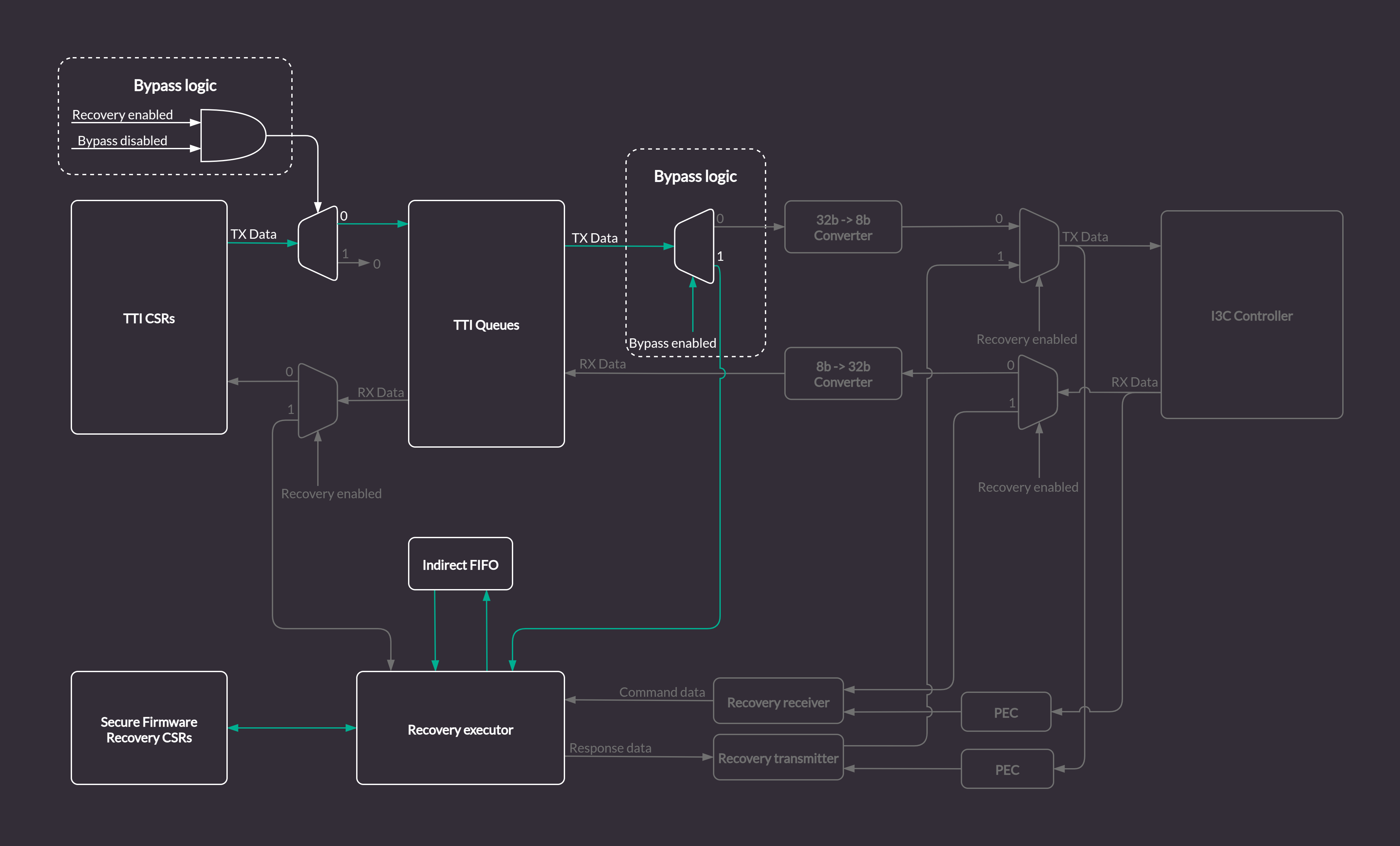
Recovery Handler with AXI bypass (green arrows show bypass data path) :::
AXI transactions may be filtered using the AXI ID field (see axi_id_filtering).
01b3839
Register descriptions
This chapter provides auto-generated register descriptions for the core.
I3CCSR address map
- Absolute Address: 0x0
- Base Offset: 0x0
- Size: 0x1000
| Offset | Identifier | Name |
|---|---|---|
| 0x000 | I3CBase | I3C Capability and Operational Registers |
| 0x080 | PIOControl | Programmable I/O |
| 0x100 | I3C_EC | Extended Capabilities |
| 0x400 | DAT | Device Address Table |
| 0x800 | DCT | Device Characteristic Table |
I3CBase register file
- Absolute Address: 0x0
- Base Offset: 0x0
- Size: 0x6C
| Offset | Identifier | Name |
|---|---|---|
| 0x00 | HCI_VERSION | HCI Version |
| 0x04 | HC_CONTROL | Control |
| 0x08 | CONTROLLER_DEVICE_ADDR | Dynamic address |
| 0x0C | HC_CAPABILITIES | Capabilities |
| 0x10 | RESET_CONTROL | Reset controls |
| 0x14 | PRESENT_STATE | Active controller |
| 0x20 | INTR_STATUS | Status |
| 0x24 | INTR_STATUS_ENABLE | Enable status reporting |
| 0x28 | INTR_SIGNAL_ENABLE | Enable status interrupts |
| 0x2C | INTR_FORCE | Force status and interrupt |
| 0x30 | DAT_SECTION_OFFSET | DAT section offset |
| 0x34 | DCT_SECTION_OFFSET | DCT section offset |
| 0x38 | RING_HEADERS_SECTION_OFFSET | Ring section offset |
| 0x3C | PIO_SECTION_OFFSET | PIO section offset |
| 0x40 | EXT_CAPS_SECTION_OFFSET | Extended capabilities section offset |
| 0x4C | INT_CTRL_CMDS_EN | MIPI commands |
| 0x58 | IBI_NOTIFY_CTRL | I3C interrupts notification |
| 0x5C | IBI_DATA_ABORT_CTRL | IBI data control |
| 0x60 | DEV_CTX_BASE_LO | Device context memory address lower 32 bits |
| 0x64 | DEV_CTX_BASE_HI | Device context memory address higher 32 bits |
| 0x68 | DEV_CTX_SG | SG control |
HCI_VERSION register
- Absolute Address: 0x0
- Base Offset: 0x0
- Size: 0x4
| Bits | Identifier | Access | Reset | Name |
|---|---|---|---|---|
| 31:0 | VERSION | r | 0x120 | — |
HC_CONTROL register
- Absolute Address: 0x4
- Base Offset: 0x4
- Size: 0x4
| Bits | Identifier | Access | Reset | Name |
|---|---|---|---|---|
| 0 | IBA_INCLUDE | rw | 0x0 | IBA_INCLUDE |
| 3 | AUTOCMD_DATA_RPT | r | 0x0 | AUTOCMD_DATA_RPT |
| 4 | DATA_BYTE_ORDER_MODE | r | 0x0 | DATA_BYTE_ORDER_MODE |
| 6 | MODE_SELECTOR | r | 0x1 | MODE_SELECTOR |
| 7 | I2C_DEV_PRESENT | rw | 0x0 | I2C_DEV_PRESENT |
| 8 | HOT_JOIN_CTRL | rw | 0x0 | HOT_JOIN_CTRL |
| 12 | HALT_ON_CMD_SEQ_TIMEOUT | rw | 0x0 | HALT_ON_CMD_SEQ_TIMEOUT |
| 29 | ABORT | rw | 0x0 | ABORT |
| 30 | RESUME | rw, woclr | 0x0 | RESUME |
| 31 | BUS_ENABLE | rw | 0x0 | BUS_ENABLE |
IBA_INCLUDE field
Include I3C Broadcast Address:
0 - skips I3C Broadcast Address for private transfers
1 - includes I3C Broadcast Address for private transfers
AUTOCMD_DATA_RPT field
Auto-Command Data Report:
0 - coalesced reporting
1 - separated reporting
DATA_BYTE_ORDER_MODE field
Data Byte Ordering Mode:
0 - Little Endian
1 - Big Endian
MODE_SELECTOR field
DMA/PIO Mode Selector:
0 - DMA
1 - PIO
I2C_DEV_PRESENT field
I2C Device Present on Bus:
0 - pure I3C bus
1 - legacy I2C devices on the bus
HOT_JOIN_CTRL field
Hot-Join ACK/NACK Control:
0 - ACK Hot-Join request
1 - NACK Hot-Join request and send Broadcast CCC to disable Hot-Join
HALT_ON_CMD_SEQ_TIMEOUT field
Halt on Command Sequence Timeout when set to 1
ABORT field
Host Controller Abort when set to 1
RESUME field
Host Controller Resume:
0 - Controller is running
1 - Controller is suspended
Write 1 to resume Controller operations.
BUS_ENABLE field
Host Controller Bus Enable
CONTROLLER_DEVICE_ADDR register
- Absolute Address: 0x8
- Base Offset: 0x8
- Size: 0x4
| Bits | Identifier | Access | Reset | Name |
|---|---|---|---|---|
| 22:16 | DYNAMIC_ADDR | rw | 0x0 | DYNAMIC_ADDR |
| 31 | DYNAMIC_ADDR_VALID | rw | 0x0 | DYNAMIC_ADDR_VALID |
DYNAMIC_ADDR field
Device Dynamic Address
DYNAMIC_ADDR_VALID field
Dynamic Address is Valid:
0 - dynamic address is invalid
1 - dynamic address is valid
HC_CAPABILITIES register
- Absolute Address: 0xC
- Base Offset: 0xC
- Size: 0x4
| Bits | Identifier | Access | Reset | Name |
|---|---|---|---|---|
| 2 | COMBO_COMMAND | r | 0x0 | COMBO_COMMAND |
| 3 | AUTO_COMMAND | r | 0x0 | AUTO_COMMAND |
| 5 | STANDBY_CR_CAP | r | 0x0 | STANDBY_CR_CAP |
| 6 | HDR_DDR_EN | r | 0x0 | HDR_DDR_EN |
| 7 | HDR_TS_EN | r | 0x0 | HDR_TS_EN |
| 10 | CMD_CCC_DEFBYTE | r | 0x1 | CMD_CCC_DEFBYTE |
| 11 | IBI_DATA_ABORT_EN | r | 0x0 | IBI_DATA_ABORT_EN |
| 12 | IBI_CREDIT_COUNT_EN | r | 0x0 | IBI_CREDIT_COUNT_EN |
| 13 | SCHEDULED_COMMANDS_EN | r | 0x0 | SCHEDULED_COMMANDS_EN |
| 21:20 | CMD_SIZE | r | 0x0 | CMD_SIZE |
| 28 | SG_CAPABILITY_CR_EN | r | 0x0 | SG_CAPABILITY_CR_EN |
| 29 | SG_CAPABILITY_IBI_EN | r | 0x0 | SG_CAPABILITY_IBI_EN |
| 30 | SG_CAPABILITY_DC_EN | r | 0x0 | SG_CAPABILITY_DC_EN |
COMBO_COMMAND field
Controller combined command:
0 - not supported
1 - supported
AUTO_COMMAND field
Automatic read command on IBI:
0 - not supported
1 - supported
STANDBY_CR_CAP field
Switching from active to standby mode:
0 - not supported, this controller is always active on I3C
1- supported, this controller can hand off I3C to secondary controller
HDR_DDR_EN field
HDR-DDR transfers:
0 - not supported
1 - supported
HDR_TS_EN field
HDR-Ternary transfers:
0 - not supported
1 - supported
CMD_CCC_DEFBYTE field
CCC with defining byte:
0 - not supported
1 - supported
IBI_DATA_ABORT_EN field
Controller IBI data abort:
0 - not supported
1 - supported
IBI_CREDIT_COUNT_EN field
Controller IBI credit count:
0 - not supported
1 - supported
SCHEDULED_COMMANDS_EN field
Controller command scheduling:
0 - not supported
1 - supported
CMD_SIZE field
Size and structure of the Command Descriptor:
2'b0: 2 DWORDs,
all other reserved.
SG_CAPABILITY_CR_EN field
DMA only: Command and Response rings memory:
0 - must be physically continuous
1 - controller supports scatter-gather
SG_CAPABILITY_IBI_EN field
DMA only: IBI status and IBI Data rings memory:
0 - must be physically continuous
1 - controller supports scatter-gather
SG_CAPABILITY_DC_EN field
Device context memory:
0 - must be physically continuous
1 - controller supports scatter-gather
RESET_CONTROL register
- Absolute Address: 0x10
- Base Offset: 0x10
- Size: 0x4
| Bits | Identifier | Access | Reset | Name |
|---|---|---|---|---|
| 0 | SOFT_RST | rw | 0x0 | SOFT_RST |
| 1 | CMD_QUEUE_RST | rw | 0x0 | CMD_QUEUE_RST |
| 2 | RESP_QUEUE_RST | rw | 0x0 | RESP_QUEUE_RST |
| 3 | TX_FIFO_RST | rw | 0x0 | TX_FIFO_RST |
| 4 | RX_FIFO_RST | rw | 0x0 | RX_FIFO_RST |
| 5 | IBI_QUEUE_RST | rw | 0x0 | IBI_QUEUE_RST |
SOFT_RST field
Reset controller from software.
CMD_QUEUE_RST field
Clear command queue from software. Valid only in PIO mode.
RESP_QUEUE_RST field
Clear response queue from software. Valid only in PIO mode.
TX_FIFO_RST field
Clear TX FIFO from software. Valid only in PIO mode.
RX_FIFO_RST field
Clear RX FIFO from software. Valid only in PIO mode.
IBI_QUEUE_RST field
Clear IBI queue from software. Valid only in PIO mode.
PRESENT_STATE register
- Absolute Address: 0x14
- Base Offset: 0x14
- Size: 0x4
| Bits | Identifier | Access | Reset | Name |
|---|---|---|---|---|
| 2 | AC_CURRENT_OWN | r | 0x0 | AC_CURRENT_OWN |
AC_CURRENT_OWN field
Controller I3C state:
0 - not bus owner
1 - bus owner
INTR_STATUS register
- Absolute Address: 0x20
- Base Offset: 0x20
- Size: 0x4
| Bits | Identifier | Access | Reset | Name |
|---|---|---|---|---|
| 10 | HC_INTERNAL_ERR_STAT | rw, woclr | 0x0 | HC_INTERNAL_ERR_STAT |
| 11 | HC_SEQ_CANCEL_STAT | rw, woclr | 0x0 | HC_SEQ_CANCEL_STAT |
| 12 | HC_WARN_CMD_SEQ_STALL_STAT | rw, woclr | 0x0 | HC_WARN_CMD_SEQ_STALL_STAT |
| 13 | HC_ERR_CMD_SEQ_TIMEOUT_STAT | rw, woclr | 0x0 | HC_ERR_CMD_SEQ_TIMEOUT_STAT |
| 14 | SCHED_CMD_MISSED_TICK_STAT | rw, woclr | 0x0 | SCHED_CMD_MISSED_TICK_STAT |
HC_INTERNAL_ERR_STAT field
Controller internal unrecoverable error.
HC_SEQ_CANCEL_STAT field
Controller had to cancel command sequence.
HC_WARN_CMD_SEQ_STALL_STAT field
Clock stalled due to lack of commands.
HC_ERR_CMD_SEQ_TIMEOUT_STAT field
Command timeout after prolonged stall.
SCHED_CMD_MISSED_TICK_STAT field
Scheduled commands could be executed due to controller being busy.
INTR_STATUS_ENABLE register
- Absolute Address: 0x24
- Base Offset: 0x24
- Size: 0x4
| Bits | Identifier | Access | Reset | Name |
|---|---|---|---|---|
| 10 | HC_INTERNAL_ERR_STAT_EN | rw | 0x0 | HC_INTERNAL_ERR_STAT_EN |
| 11 | HC_SEQ_CANCEL_STAT_EN | rw | 0x0 | HC_SEQ_CANCEL_STAT_EN |
| 12 | HC_WARN_CMD_SEQ_STALL_STAT_EN | rw | 0x0 | HC_WARN_CMD_SEQ_STALL_STAT_EN |
| 13 | HC_ERR_CMD_SEQ_TIMEOUT_STAT_EN | rw | 0x0 | HC_ERR_CMD_SEQ_TIMEOUT_STAT_EN |
| 14 | SCHED_CMD_MISSED_TICK_STAT_EN | rw | 0x0 | SCHED_CMD_MISSED_TICK_STAT_EN |
HC_INTERNAL_ERR_STAT_EN field
Enable HC_INTERNAL_ERR_STAT monitoring.
HC_SEQ_CANCEL_STAT_EN field
Enable HC_SEQ_CANCEL_STAT monitoring.
HC_WARN_CMD_SEQ_STALL_STAT_EN field
Enable HC_WARN_CMD_SEQ_STALL_STAT monitoring.
HC_ERR_CMD_SEQ_TIMEOUT_STAT_EN field
Enable HC_ERR_CMD_SEQ_TIMEOUT_STAT monitoring.
SCHED_CMD_MISSED_TICK_STAT_EN field
Enable SCHED_CMD_MISSED_TICK_STAT monitoring.
INTR_SIGNAL_ENABLE register
- Absolute Address: 0x28
- Base Offset: 0x28
- Size: 0x4
| Bits | Identifier | Access | Reset | Name |
|---|---|---|---|---|
| 10 | HC_INTERNAL_ERR_SIGNAL_EN | rw | 0x0 | HC_INTERNAL_ERR_SIGNAL_EN |
| 11 | HC_SEQ_CANCEL_SIGNAL_EN | rw | 0x0 | HC_SEQ_CANCEL_SIGNAL_EN |
| 12 | HC_WARN_CMD_SEQ_STALL_SIGNAL_EN | rw | 0x0 | HC_WARN_CMD_SEQ_STALL_SIGNAL_EN |
| 13 | HC_ERR_CMD_SEQ_TIMEOUT_SIGNAL_EN | rw | 0x0 | HC_ERR_CMD_SEQ_TIMEOUT_SIGNAL_EN |
| 14 | SCHED_CMD_MISSED_TICK_SIGNAL_EN | rw | 0x0 | SCHED_CMD_MISSED_TICK_SIGNAL_EN |
HC_INTERNAL_ERR_SIGNAL_EN field
Enable HC_INTERNAL_ERR_STAT interrupt.
HC_SEQ_CANCEL_SIGNAL_EN field
Enable HC_SEQ_CANCEL_STAT interrupt.
HC_WARN_CMD_SEQ_STALL_SIGNAL_EN field
Enable HC_WARN_CMD_SEQ_STALL_STAT interrupt.
HC_ERR_CMD_SEQ_TIMEOUT_SIGNAL_EN field
Enable HC_ERR_CMD_SEQ_TIMEOUT_STAT interrupt.
SCHED_CMD_MISSED_TICK_SIGNAL_EN field
Enable SCHED_CMD_MISSED_TICK_STAT interrupt.
INTR_FORCE register
- Absolute Address: 0x2C
- Base Offset: 0x2C
- Size: 0x4
| Bits | Identifier | Access | Reset | Name |
|---|---|---|---|---|
| 10 | HC_INTERNAL_ERR_FORCE | w | 0x0 | HC_INTERNAL_ERR_FORCE |
| 11 | HC_SEQ_CANCEL_FORCE | w | 0x0 | HC_SEQ_CANCEL_FORCE |
| 12 | HC_WARN_CMD_SEQ_STALL_FORCE | w | 0x0 | HC_WARN_CMD_SEQ_STALL_FORCE |
| 13 | HC_ERR_CMD_SEQ_TIMEOUT_FORCE | w | 0x0 | HC_ERR_CMD_SEQ_TIMEOUT_FORCE |
| 14 | SCHED_CMD_MISSED_TICK_FORCE | w | 0x0 | SCHED_CMD_MISSED_TICK_FORCE |
HC_INTERNAL_ERR_FORCE field
Force HC_INTERNAL_ERR_STAT interrupt.
HC_SEQ_CANCEL_FORCE field
Force HC_SEQ_CANCEL_STAT interrupt.
HC_WARN_CMD_SEQ_STALL_FORCE field
Force HC_WARN_CMD_SEQ_STALL_STAT interrupt.
HC_ERR_CMD_SEQ_TIMEOUT_FORCE field
Force HC_ERR_CMD_SEQ_TIMEOUT_STAT interrupt.
SCHED_CMD_MISSED_TICK_FORCE field
Force SCHED_CMD_MISSED_TICK_STAT interrupt.
DAT_SECTION_OFFSET register
- Absolute Address: 0x30
- Base Offset: 0x30
- Size: 0x4
| Bits | Identifier | Access | Reset | Name |
|---|---|---|---|---|
| 11:0 | TABLE_OFFSET | r | 0x400 | TABLE_OFFSET |
| 18:12 | TABLE_SIZE | r | 0x7F | TABLE_SIZE |
| 31:28 | ENTRY_SIZE | r | 0x0 | ENTRY_SIZE |
TABLE_OFFSET field
DAT entry offset in respect to BASE address.
TABLE_SIZE field
Max number of DAT entries.
ENTRY_SIZE field
Individual DAT entry size. 0 - 2 DWRODs, 1:15 - reserved.
DCT_SECTION_OFFSET register
- Absolute Address: 0x34
- Base Offset: 0x34
- Size: 0x4
| Bits | Identifier | Access | Reset | Name |
|---|---|---|---|---|
| 11:0 | TABLE_OFFSET | r | 0x800 | TABLE_OFFSET |
| 18:12 | TABLE_SIZE | r | 0x7F | TABLE_SIZE |
| 23:19 | TABLE_INDEX | rw | 0x0 | TABLE_INDEX |
| 31:28 | ENTRY_SIZE | r | 0x0 | ENTRY_SIZE |
TABLE_OFFSET field
DCT entry offset in respect to BASE address.
TABLE_SIZE field
Max number of DCT entries.
TABLE_INDEX field
Index to DCT used during ENTDAA.
ENTRY_SIZE field
Individual DCT entry size.
0 - 4 DWORDs,
1:15 - Reserved.
RING_HEADERS_SECTION_OFFSET register
- Absolute Address: 0x38
- Base Offset: 0x38
- Size: 0x4
| Bits | Identifier | Access | Reset | Name |
|---|---|---|---|---|
| 15:0 | SECTION_OFFSET | r | 0x0 | SECTION_OFFSET |
SECTION_OFFSET field
DMA ring headers section offset. Invalid if 0.
PIO_SECTION_OFFSET register
- Absolute Address: 0x3C
- Base Offset: 0x3C
- Size: 0x4
| Bits | Identifier | Access | Reset | Name |
|---|---|---|---|---|
| 15:0 | SECTION_OFFSET | r | 0x80 | SECTION_OFFSET |
SECTION_OFFSET field
PIO section offset. Invalid if 0.
EXT_CAPS_SECTION_OFFSET register
- Absolute Address: 0x40
- Base Offset: 0x40
- Size: 0x4
| Bits | Identifier | Access | Reset | Name |
|---|---|---|---|---|
| 15:0 | SECTION_OFFSET | r | 0x100 | SECTION_OFFSET |
SECTION_OFFSET field
Extended Capabilities section offset. Invalid if 0.
INT_CTRL_CMDS_EN register
- Absolute Address: 0x4C
- Base Offset: 0x4C
- Size: 0x4
| Bits | Identifier | Access | Reset | Name |
|---|---|---|---|---|
| 0 | ICC_SUPPORT | r | 0x1 | ICC_SUPPORT |
| 15:1 | MIPI_CMDS_SUPPORTED | r | 0x35 | MIPI_CMDS_SUPPORTED |
ICC_SUPPORT field
Internal Control Commands:
1 - some or all internals commands sub-commands are supported,
0 - illegal.
MIPI_CMDS_SUPPORTED field
Bitmask of supported MIPI commands.
IBI_NOTIFY_CTRL register
- Absolute Address: 0x58
- Base Offset: 0x58
- Size: 0x4
| Bits | Identifier | Access | Reset | Name |
|---|---|---|---|---|
| 0 | NOTIFY_HJ_REJECTED | rw | 0x0 | NOTIFY_HJ_REJECTED |
| 1 | NOTIFY_CRR_REJECTED | rw | 0x0 | NOTIFY_CRR_REJECTED |
| 3 | NOTIFY_IBI_REJECTED | rw | 0x0 | NOTIFY_IBI_REJECTED |
NOTIFY_HJ_REJECTED field
Notify about rejected hot-join:
0 - do not enqueue rejected HJ,
1 = enqueue rejected HJ on IBI queue/ring.
NOTIFY_CRR_REJECTED field
Notify about rejected controller role request:
0 - do not enqueue rejected CRR,
1 = enqueue rejected CRR on IBI queue/ring.
NOTIFY_IBI_REJECTED field
Notify about rejected IBI:
0 - do not enqueue rejected IBI,
1 = enqueue rejected IBI on IBI queue/ring.
IBI_DATA_ABORT_CTRL register
- Absolute Address: 0x5C
- Base Offset: 0x5C
- Size: 0x4
| Bits | Identifier | Access | Reset | Name |
|---|---|---|---|---|
| 15:8 | MATCH_IBI_ID | rw | 0x0 | MATCH_IBI_ID |
| 17:16 | AFTER_N_CHUNKS | rw | 0x0 | AFTER_N_CHUNKS |
| 20:18 | MATCH_STATUS_TYPE | rw | 0x0 | MATCH_STATUS_TYPE |
| 31 | IBI_DATA_ABORT_MON | rw | 0x0 | IBI_DATA_ABORT_MON |
MATCH_IBI_ID field
IBI target address:
[15:9] - device address,
[8] - must always be set to 1'b1
AFTER_N_CHUNKS field
Number of data chunks to be allowed before forced termination:
0 - immediate,
1:3 - delay by 1-3 data chunks.
MATCH_STATUS_TYPE field
Define which IBI should be aborted:
3'b000 - Regular IBI,
3'b100 - Autocmd IBI,
other values - not supported.
IBI_DATA_ABORT_MON field
Enable/disable IBI monitoring logic.
DEV_CTX_BASE_LO register
- Absolute Address: 0x60
- Base Offset: 0x60
- Size: 0x4
| Bits | Identifier | Access | Reset | Name |
|---|---|---|---|---|
| 0 | BASE_LO | rw | 0x0 | — |
DEV_CTX_BASE_HI register
- Absolute Address: 0x64
- Base Offset: 0x64
- Size: 0x4
| Bits | Identifier | Access | Reset | Name |
|---|---|---|---|---|
| 0 | BASE_HI | rw | 0x0 | — |
DEV_CTX_SG register
- Absolute Address: 0x68
- Base Offset: 0x68
- Size: 0x4
| Bits | Identifier | Access | Reset | Name |
|---|---|---|---|---|
| 15:0 | LIST_SIZE | r | 0x0 | LIST_SIZE |
| 31 | BLP | r | 0x0 | BLP |
LIST_SIZE field
Number of SG entries.
BLP field
Buffer vs list pointer in device context:
0 - continuous physical memory region,
1 - pointer to SG descriptor list.
PIOControl register file
- Absolute Address: 0x80
- Base Offset: 0x80
- Size: 0x34
| Offset | Identifier | Name |
|---|---|---|
| 0x00 | COMMAND_PORT | Command issue port |
| 0x04 | RESPONSE_PORT | Command response port |
| 0x08 | TX_DATA_PORT | Transferred data access port |
| 0x08 | RX_DATA_PORT | Received data access port |
| 0x0C | IBI_PORT | IBI descriptor access port |
| 0x10 | QUEUE_THLD_CTRL | The Queue Threshold Control register for the Command Queue, the Response Queue, and the IBI Queue |
| 0x14 | DATA_BUFFER_THLD_CTRL | RX/TX queue threshold control |
| 0x18 | QUEUE_SIZE | Queue sizes |
| 0x1C | ALT_QUEUE_SIZE | Alternate queue sizes |
| 0x20 | PIO_INTR_STATUS | PIO interrupt status |
| 0x24 | PIO_INTR_STATUS_ENABLE | — |
| 0x28 | PIO_INTR_SIGNAL_ENABLE | Interrupt Signal Enable |
| 0x2C | PIO_INTR_FORCE | PIO force interrupt status |
| 0x30 | PIO_CONTROL | PIO control |
COMMAND_PORT register
- Absolute Address: 0x80
- Base Offset: 0x0
- Size: 0x4
| Bits | Identifier | Access | Reset | Name |
|---|---|---|---|---|
| 31:0 | COMMAND_DATA | w | — | COMMAND_QUEUE_PORT |
RESPONSE_PORT register
- Absolute Address: 0x84
- Base Offset: 0x4
- Size: 0x4
| Bits | Identifier | Access | Reset | Name |
|---|---|---|---|---|
| 31:0 | RESPONSE_DATA | r | — | RESPONSE_QUEUE_PORT |
TX_DATA_PORT register
- Absolute Address: 0x88
- Base Offset: 0x8
- Size: 0x4
| Bits | Identifier | Access | Reset | Name |
|---|---|---|---|---|
| 31:0 | TX_DATA | w | — | TX_DATA |
RX_DATA_PORT register
- Absolute Address: 0x88
- Base Offset: 0x8
- Size: 0x4
| Bits | Identifier | Access | Reset | Name |
|---|---|---|---|---|
| 31:0 | RX_DATA | r | — | RX_DATA |
IBI_PORT register
- Absolute Address: 0x8C
- Base Offset: 0xC
- Size: 0x4
| Bits | Identifier | Access | Reset | Name |
|---|---|---|---|---|
| 31:0 | IBI_DATA | r | — | IBI_DATA |
IBI_DATA field
Data Read from IBI Data Buffer.
The IBI Port is mapped to the IBI Data Queue. IBI Data is always aligned to a 4-byte boundary and then put into the IBI Queue. If the incoming data is not aligned to a 4-byte boundary, then there will be extra (unused) bytes at the end of the transferred IBI data. This can be determined from the value of field DATA_LENGTH in the IBI Status Descriptor.
QUEUE_THLD_CTRL register
- Absolute Address: 0x90
- Base Offset: 0x10
- Size: 0x4
| Bits | Identifier | Access | Reset | Name |
|---|---|---|---|---|
| 7:0 | CMD_EMPTY_BUF_THLD | rw | 0x1 | CMD_EMPTY_BUF_THLD |
| 15:8 | RESP_BUF_THLD | rw | 0x1 | RESP_BUF_THLD |
| 23:16 | IBI_DATA_SEGMENT_SIZE | rw | 0x1 | IBI_DATA_SEGMENT_SIZE |
| 31:24 | IBI_STATUS_THLD | rw | 0x1 | IBI_STATUS_THLD |
CMD_EMPTY_BUF_THLD field
Triggers CMD_QUEUE_READY_STAT interrupt when CMD queue has N or more free entries. Accepted values are 1:255
RESP_BUF_THLD field
Triggers RESP_READY_STAT interrupt when RESP queue has N or more entries. Accepted values are 1:255
IBI_DATA_SEGMENT_SIZE field
IBI Queue data segment size. Valida values are 1:63
IBI_STATUS_THLD field
Triggers IBI_STATUS_THLD_STAT interrupt when IBI queue has N or more entries. Accepted values are 1:255
DATA_BUFFER_THLD_CTRL register
- Absolute Address: 0x94
- Base Offset: 0x14
- Size: 0x4
| Bits | Identifier | Access | Reset | Name |
|---|---|---|---|---|
| 2:0 | TX_BUF_THLD | rw | 0x1 | TX_BUF_THLD |
| 10:8 | RX_BUF_THLD | rw | 0x1 | RX_BUF_THLD |
| 18:16 | TX_START_THLD | rw | 0x1 | TX_START_THLD |
| 26:24 | RX_START_THLD | rw | 0x1 | RX_START_THLD |
TX_BUF_THLD field
Trigger TX_THLD_STAT interrupt when TX queue has 2^(N+1) or more free entries
RX_BUF_THLD field
Trigger RX_THLD_STAT interrupt when RX queue has 2^(N+1) or more entries
TX_START_THLD field
Postpone write command until TX queue has 2^(N+1) entries
RX_START_THLD field
Postpone read command until RX queue has 2^(N+1) free entries
QUEUE_SIZE register
- Absolute Address: 0x98
- Base Offset: 0x18
- Size: 0x4
| Bits | Identifier | Access | Reset | Name |
|---|---|---|---|---|
| 7:0 | CR_QUEUE_SIZE | r | 0x40 | CR_QUEUE_SIZE |
| 15:8 | IBI_STATUS_SIZE | r | 0x40 | IBI_STATUS_SIZE |
| 23:16 | RX_DATA_BUFFER_SIZE | r | 0x5 | RX_DATA_BUFFER_SIZE |
| 31:24 | TX_DATA_BUFFER_SIZE | r | 0x5 | TX_DATA_BUFFER_SIZE |
CR_QUEUE_SIZE field
Command/Response queue size is equal to N
IBI_STATUS_SIZE field
IBI Queue size is equal to N
RX_DATA_BUFFER_SIZE field
RX queue size is equal to 2^(N+1), where N is this field value
TX_DATA_BUFFER_SIZE field
TX queue size is equal to 2^(N+1), where N is this field value
ALT_QUEUE_SIZE register
- Absolute Address: 0x9C
- Base Offset: 0x1C
- Size: 0x4
| Bits | Identifier | Access | Reset | Name |
|---|---|---|---|---|
| 7:0 | ALT_RESP_QUEUE_SIZE | r | 0x40 | ALT_RESP_QUEUE_SIZE |
| 24 | ALT_RESP_QUEUE_EN | r | 0x0 | ALT_RESP_QUEUE_EN |
| 28 | EXT_IBI_QUEUE_EN | r | 0x0 | EXT_IBI_QUEUE_EN |
ALT_RESP_QUEUE_SIZE field
Valid only if ALT_RESP_QUEUE_EN is set. Contains response queue size
ALT_RESP_QUEUE_EN field
If set, response and command queues are not equal lengths, then ALT_RESP_QUEUE_SIZE contains response queue size
EXT_IBI_QUEUE_EN field
1 indicates that IBI queue size is equal to 8*IBI_STATUS_SIZE
PIO_INTR_STATUS register
- Absolute Address: 0xA0
- Base Offset: 0x20
- Size: 0x4
| Bits | Identifier | Access | Reset | Name |
|---|---|---|---|---|
| 0 | TX_THLD_STAT | r | 0x0 | TX_THLD_STAT |
| 1 | RX_THLD_STAT | r | 0x0 | RX_THLD_STAT |
| 2 | IBI_STATUS_THLD_STAT | r | 0x0 | IBI_STATUS_THLD_STAT |
| 3 | CMD_QUEUE_READY_STAT | r | 0x0 | CMD_QUEUE_READY_STAT |
| 4 | RESP_READY_STAT | r | 0x0 | RESP_READY_STAT |
| 5 | TRANSFER_ABORT_STAT | rw, woclr | 0x0 | TRANSFER_ABORT_STAT |
| 9 | TRANSFER_ERR_STAT | rw, woclr | 0x0 | TRANSFER_ERR_STAT |
TX_THLD_STAT field
TX queue fulfils TX_BUF_THLD
RX_THLD_STAT field
RX queue fulfils RX_BUF_THLD
IBI_STATUS_THLD_STAT field
IBI queue fulfils IBI_STATUS_THLD
CMD_QUEUE_READY_STAT field
Command queue fulfils CMD_EMPTY_BUF_THLD
RESP_READY_STAT field
Response queue fulfils RESP_BUF_THLD
TRANSFER_ABORT_STAT field
Transfer aborted
TRANSFER_ERR_STAT field
Transfer error
PIO_INTR_STATUS_ENABLE register
- Absolute Address: 0xA4
- Base Offset: 0x24
- Size: 0x4
| Bits | Identifier | Access | Reset | Name |
|---|---|---|---|---|
| 0 | TX_THLD_STAT_EN | rw | 0x0 | TX_THLD_STAT_EN |
| 1 | RX_THLD_STAT_EN | rw | 0x0 | RX_THLD_STAT_EN |
| 2 | IBI_STATUS_THLD_STAT_EN | rw | 0x0 | IBI_STATUS_THLD_STAT_EN |
| 3 | CMD_QUEUE_READY_STAT_EN | rw | 0x0 | CMD_QUEUE_READY_STAT_EN |
| 4 | RESP_READY_STAT_EN | rw | 0x0 | RESP_READY_STAT_EN |
| 5 | TRANSFER_ABORT_STAT_EN | rw | 0x0 | TRANSFER_ABORT_STAT_EN |
| 9 | TRANSFER_ERR_STAT_EN | rw | 0x0 | TRANSFER_ERR_STAT_EN |
TX_THLD_STAT_EN field
Enable TX queue monitoring
RX_THLD_STAT_EN field
Enable RX queue monitoring
IBI_STATUS_THLD_STAT_EN field
Enable IBI queue monitoring
CMD_QUEUE_READY_STAT_EN field
Enable command queue monitoring
RESP_READY_STAT_EN field
Enable response queue monitoring
TRANSFER_ABORT_STAT_EN field
Enable transfer abort monitoring
TRANSFER_ERR_STAT_EN field
Enable transfer error monitoring
PIO_INTR_SIGNAL_ENABLE register
- Absolute Address: 0xA8
- Base Offset: 0x28
- Size: 0x4
| Bits | Identifier | Access | Reset | Name |
|---|---|---|---|---|
| 0 | TX_THLD_SIGNAL_EN | rw | 0x0 | TX_THLD_SIGNAL_EN |
| 1 | RX_THLD_SIGNAL_EN | rw | 0x0 | RX_THLD_SIGNAL_EN |
| 2 | IBI_STATUS_THLD_SIGNAL_EN | rw | 0x0 | IBI_STATUS_THLD_SIGNAL_EN |
| 3 | CMD_QUEUE_READY_SIGNAL_EN | rw | 0x0 | CMD_QUEUE_READY_SIGNAL_EN |
| 4 | RESP_READY_SIGNAL_EN | rw | 0x0 | RESP_READY_SIGNAL_EN |
| 5 | TRANSFER_ABORT_SIGNAL_EN | rw | 0x0 | TRANSFER_ABORT_SIGNAL_EN |
| 9 | TRANSFER_ERR_SIGNAL_EN | rw | 0x0 | TRANSFER_ERR_SIGNAL_EN |
TX_THLD_SIGNAL_EN field
Enable TX queue interrupt
RX_THLD_SIGNAL_EN field
Enable RX queue interrupt
IBI_STATUS_THLD_SIGNAL_EN field
Enable IBI queue interrupt
CMD_QUEUE_READY_SIGNAL_EN field
Enable command queue interrupt
RESP_READY_SIGNAL_EN field
Enable response ready interrupt
TRANSFER_ABORT_SIGNAL_EN field
Enable transfer abort interrupt
TRANSFER_ERR_SIGNAL_EN field
Enable transfer error interrupt
PIO_INTR_FORCE register
- Absolute Address: 0xAC
- Base Offset: 0x2C
- Size: 0x4
| Bits | Identifier | Access | Reset | Name |
|---|---|---|---|---|
| 0 | TX_THLD_FORCE | w | 0x0 | TX_THLD_FORCE |
| 1 | RX_THLD_FORCE | w | 0x0 | RX_THLD_FORCE |
| 2 | IBI_THLD_FORCE | w | 0x0 | IBI_THLD_FORCE |
| 3 | CMD_QUEUE_READY_FORCE | w | 0x0 | CMD_QUEUE_READY_FORCE |
| 4 | RESP_READY_FORCE | w | 0x0 | RESP_READY_FORCE |
| 5 | TRANSFER_ABORT_FORCE | w | 0x0 | TRANSFER_ABORT_FORCE |
| 9 | TRANSFER_ERR_FORCE | w | 0x0 | TRANSFER_ERR_FORCE |
TX_THLD_FORCE field
Force TX queue interrupt
RX_THLD_FORCE field
Force RX queue interrupt
IBI_THLD_FORCE field
Force IBI queue interrupt
CMD_QUEUE_READY_FORCE field
Force command queue interrupt
RESP_READY_FORCE field
Force response queue interrupt
TRANSFER_ABORT_FORCE field
Force transfer aborted
TRANSFER_ERR_FORCE field
Force transfer error
PIO_CONTROL register
- Absolute Address: 0xB0
- Base Offset: 0x30
- Size: 0x4
| Bits | Identifier | Access | Reset | Name |
|---|---|---|---|---|
| 0 | ENABLE | rw | 0x1 | ENABLE |
| 1 | RS | rw | 0x0 | RS |
| 2 | ABORT | rw | 0x0 | ABORT |
ENABLE field
Enables PIO queues. When disabled, SW may not read from/write to PIO queues. 1 - PIO queue enable request, 0 - PIO queue disable request
RS field
Run/Stop execution of enqueued commands. When set to 0, it holds execution of enqueued commands and runs current command to completion. 1 - PIO Queue start request, 0 - PIO Queue stop request.
ABORT field
Stop current command descriptor execution forcefully and hold remaining commands. 1 - Request PIO Abort, 0 - Resume PIO execution
I3C_EC register file
- Absolute Address: 0x100
- Base Offset: 0x100
- Size: 0x274
| Offset | Identifier | Name |
|---|---|---|
| 0x000 | SecFwRecoveryIf | Secure Firmware Recovery Interface |
| 0x080 | StdbyCtrlMode | Standby Controller Mode |
| 0x100 | TTI | Target Transaction Interface |
| 0x200 | SoCMgmtIf | SoC Management Interface |
| 0x268 | CtrlCfg | Controller Config |
| 0x270 | TERMINATION_EXTCAP_HEADER | — |
SecFwRecoveryIf register file
- Absolute Address: 0x100
- Base Offset: 0x0
- Size: 0x6C
| Offset | Identifier | Name |
|---|---|---|
| 0x00 | EXTCAP_HEADER | — |
| 0x04 | PROT_CAP_0 | Recovery Protocol Capabilities 0 |
| 0x08 | PROT_CAP_1 | Recovery Protocol Capabilities 1 |
| 0x0C | PROT_CAP_2 | Recovery Protocol Capabilities 2 |
| 0x10 | PROT_CAP_3 | Recovery Protocol Capabilities 3 |
| 0x14 | DEVICE_ID_0 | Device Identification 0 |
| 0x18 | DEVICE_ID_1 | Device Identification 1 |
| 0x1C | DEVICE_ID_2 | Device Identification 2 |
| 0x20 | DEVICE_ID_3 | Device Identification 3 |
| 0x24 | DEVICE_ID_4 | Device Identification 4 |
| 0x28 | DEVICE_ID_5 | Device Identification 5 |
| 0x2C | DEVICE_ID_RESERVED | Reserved |
| 0x30 | DEVICE_STATUS_0 | Device status 0 |
| 0x34 | DEVICE_STATUS_1 | Device status 1 |
| 0x38 | DEVICE_RESET | Reset control |
| 0x3C | RECOVERY_CTRL | Recovery configuration/control |
| 0x40 | RECOVERY_STATUS | Recovery status |
| 0x44 | HW_STATUS | Hardware status |
| 0x48 | INDIRECT_FIFO_CTRL_0 | Indirect FIFO Control 0 |
| 0x4C | INDIRECT_FIFO_CTRL_1 | Indirect FIFO Control 1 |
| 0x50 | INDIRECT_FIFO_STATUS_0 | Indirect FIFO Status 0 |
| 0x54 | INDIRECT_FIFO_STATUS_1 | Indirect FIFO Status 1 |
| 0x58 | INDIRECT_FIFO_STATUS_2 | Indirect FIFO Status 2 |
| 0x5C | INDIRECT_FIFO_STATUS_3 | Indirect FIFO Status 3 |
| 0x60 | INDIRECT_FIFO_STATUS_4 | Indirect FIFO Status 4 |
| 0x64 | INDIRECT_FIFO_RESERVED | INDIRECT_FIFO_RESERVED |
| 0x68 | INDIRECT_FIFO_DATA | INDIRECT_FIFO_DATA |
EXTCAP_HEADER register
- Absolute Address: 0x100
- Base Offset: 0x0
- Size: 0x4
| Bits | Identifier | Access | Reset | Name |
|---|---|---|---|---|
| 7:0 | CAP_ID | r | 0xC0 | CAP_ID |
| 23:8 | CAP_LENGTH | r | 0x20 | CAP_LENGTH |
CAP_ID field
Extended Capability ID
CAP_LENGTH field
Capability Structure Length in DWORDs
PROT_CAP_0 register
- Absolute Address: 0x104
- Base Offset: 0x4
- Size: 0x4
| Bits | Identifier | Access | Reset | Name |
|---|---|---|---|---|
| 31:0 | REC_MAGIC_STRING_0 | r | 0x2050434F | Recovery protocol magic string |
REC_MAGIC_STRING_0 field
Magic string 'OCP ' (1st part of 'OCP RECV') in ASCII code - '0x4f 0x43 0x50 0x20'
PROT_CAP_1 register
- Absolute Address: 0x108
- Base Offset: 0x8
- Size: 0x4
| Bits | Identifier | Access | Reset | Name |
|---|---|---|---|---|
| 31:0 | REC_MAGIC_STRING_1 | r | 0x56434552 | Recovery protocol magic string |
REC_MAGIC_STRING_1 field
Magic string 'RECV' (2nd part of 'OCP RECV') in ASCII code - '0x52 0x45 0x43 0x56'
PROT_CAP_2 register
- Absolute Address: 0x10C
- Base Offset: 0xC
- Size: 0x4
| Bits | Identifier | Access | Reset | Name |
|---|---|---|---|---|
| 15:0 | REC_PROT_VERSION | rw | 0x0 | Recovery protocol version |
| 31:16 | AGENT_CAPS | rw | 0x0 | Recovery protocol capabilities |
REC_PROT_VERSION field
-
Byte 0: Major version number = 0x1
-
Byte 1: Minor version number = 0x1
AGENT_CAPS field
Agent capabilities:
-
bit 0: Identification (DEVICE_ID structure)
-
bit 1: Forced Recovery (From RESET)
-
bit 2: Mgmt reset (From RESET)
-
bit 3: Device Reset (From RESET)
-
bit 4: Device status (DEVICE_STATUS)
-
bit 5: Recovery memory access (INDIRECT_CTRL)
-
bit 6: Local C-image support
-
bit 7: Push C-image support
-
bit 8: Interface isolation
-
bit 9: Hardware status
-
bit 10: Vendor command
-
bit 11: Flashless boot (From RESET)
-
bit 12: FIFO CMS support (INDIRECT_FIFO_CTRL)
-
bits 13-15: Reserved
PROT_CAP_3 register
- Absolute Address: 0x110
- Base Offset: 0x10
- Size: 0x4
| Bits | Identifier | Access | Reset | Name |
|---|---|---|---|---|
| 7:0 | NUM_OF_CMS_REGIONS | rw | 0x0 | Total number of CMS regions |
| 15:8 | MAX_RESP_TIME | rw | 0x0 | Maximum Response Time |
| 23:16 | HEARTBEAT_PERIOD | rw | 0x0 | Heartbeat Period |
NUM_OF_CMS_REGIONS field
0-255: The total number of component memory space (CMS) regions a device supports. This number includes any logging, code and vendor defined regions
MAX_RESP_TIME field
0-255: Maximum response time in 2^x microseconds(us).
HEARTBEAT_PERIOD field
0-255: Heartbeat period, 2^x microseconds (us), 0 indicates not supported
DEVICE_ID_0 register
- Absolute Address: 0x114
- Base Offset: 0x14
- Size: 0x4
| Bits | Identifier | Access | Reset | Name |
|---|---|---|---|---|
| 7:0 | DESC_TYPE | rw | 0x0 | Initial descriptor type |
| 15:8 | VENDOR_SPECIFIC_STR_LENGTH | rw | 0x0 | Vendor Specific String Length |
| 31:16 | DATA | rw | 0x0 |
DESC_TYPE field
Based on table 8 from [DMTF PLDM FM]:
-
0x00: PCI Vendor
-
0x1: IANA
-
0x2: UUID
-
0x3: PnP Vendor
-
0x4: ACPI Vendor
-
0x5: IANA Enterprise Type
-
0x6-0xFE: Reserved
-
0xFF: NVMe-MI
VENDOR_SPECIFIC_STR_LENGTH field
0x0-0xFF: Total length of Vendor Specific String, 0 indicates not supported
DATA field
DEVICE_ID_1 register
- Absolute Address: 0x118
- Base Offset: 0x18
- Size: 0x4
| Bits | Identifier | Access | Reset | Name |
|---|---|---|---|---|
| 31:0 | DATA | rw | 0x0 |
DATA field
DEVICE_ID_2 register
- Absolute Address: 0x11C
- Base Offset: 0x1C
- Size: 0x4
| Bits | Identifier | Access | Reset | Name |
|---|---|---|---|---|
| 31:0 | DATA | rw | 0x0 |
DATA field
DEVICE_ID_3 register
- Absolute Address: 0x120
- Base Offset: 0x20
- Size: 0x4
| Bits | Identifier | Access | Reset | Name |
|---|---|---|---|---|
| 31:0 | DATA | rw | 0x0 |
DATA field
DEVICE_ID_4 register
- Absolute Address: 0x124
- Base Offset: 0x24
- Size: 0x4
| Bits | Identifier | Access | Reset | Name |
|---|---|---|---|---|
| 31:0 | DATA | rw | 0x0 |
DATA field
DEVICE_ID_5 register
- Absolute Address: 0x128
- Base Offset: 0x28
- Size: 0x4
| Bits | Identifier | Access | Reset | Name |
|---|---|---|---|---|
| 31:0 | DATA | rw | 0x0 |
DATA field
DEVICE_ID_RESERVED register
- Absolute Address: 0x12C
- Base Offset: 0x2C
- Size: 0x4
| Bits | Identifier | Access | Reset | Name |
|---|---|---|---|---|
| 31:0 | DATA | r | 0x0 |
DATA field
DEVICE_STATUS_0 register
- Absolute Address: 0x130
- Base Offset: 0x30
- Size: 0x4
| Bits | Identifier | Access | Reset | Name |
|---|---|---|---|---|
| 7:0 | DEV_STATUS | rw | 0x0 | Device status |
| 15:8 | PROT_ERROR | rw, rclr | 0x0 | Protocol Error |
| 31:16 | REC_REASON_CODE | rw | 0x0 | Recovery Reason Codes |
DEV_STATUS field
-
0x0: Status Pending (Recover Reason Code not populated)
-
0x1: Device healthy (Recover Reason Code not populated)
-
0x2: Device Error (“soft” error or other error state) - (Recover Reason Code not populated)
-
0x3: Recovery mode - ready to accept recovery image - (Recover Reason Code populated)
-
0x4: Recovery Pending (waiting for activation) - (Recover Reason Code populated)
-
0x5: Running Recovery Image ( Recover Reason Code not populated)
-
0x6-0xD: Reserved
-
0xE: Boot Failure (Recover Reason Code populated)
-
0xF: Fatal Error (Recover Reason Code not populated)
-
0x10-FF:Reserved
PROT_ERROR field
-
0x0: No Protocol Error
-
0x1: Unsupported/Write Command - command is not support or a write to a RO command
-
0x2: Unsupported Parameter
-
0x3: Length write error (length of write command is incorrect)
-
0x4: CRC Error (if supported)
-
0x5-0xFE: Reserved
-
0xFF: General Protocol Error - catch all unclassified errors
REC_REASON_CODE field
-
0x0: No Boot Failure detected (BFNF)
-
0x1: Generic hardware error (BFGHWE)
-
0x2: Generic hardware soft error (BFGSE) - soft error may be recoverable
-
0x3: Self-test failure (BFSTF) (e.g., RSA self test failure, FIPs self test failure,, etc.)
-
0x4: Corrupted/missing critical data (BFCD)
-
0x5: Missing/corrupt key manifest (BFKMMC)
-
0x6: Authentication Failure on key manifest (BFKMAF)
-
0x7: Anti-rollback failure on key manifest (BFKIAR)
-
0x8: Missing/corrupt boot loader (first mutable code) firmware image (BFFIMC)
-
0x9: Authentication failure on boot loader ( 1st mutable code) firmware image (BFFIAF)
-
0xA: Anti-rollback failure boot loader (1st mutable code) firmware image (BFFIAR)
-
0xB: Missing/corrupt main/management firmware image (BFMFMC)
-
0xC: Authentication Failure main/management firmware image (BFMFAF)
-
0xD: Anti-rollback Failure main/management firmware image (BFMFAR)
-
0xE: Missing/corrupt recovery firmware (BFRFMC)
-
0xF: Authentication Failure recovery firmware (BFRFAF)
-
0x10: Anti-rollback Failure on recovery firmware (BFRFAR)
-
0x11: Forced Recovery (FR)
-
0x12: Flashless/Streaming Boot (FSB)
-
0x13-0x7F: Reserved
-
0x80-0xFF: Vendor Unique Boot Failure Codes
DEVICE_STATUS_1 register
- Absolute Address: 0x134
- Base Offset: 0x34
- Size: 0x4
| Bits | Identifier | Access | Reset | Name |
|---|---|---|---|---|
| 15:0 | HEARTBEAT | rw | 0x0 | Heartbeat |
| 24:16 | VENDOR_STATUS_LENGTH | rw | 0x0 | Vendor Status Length |
| 31:25 | VENDOR_STATUS | rw | 0x0 | Vendor defined status message |
HEARTBEAT field
0-4095: Incrementing number (counter wraps)
VENDOR_STATUS_LENGTH field
0-248: Length in bytes of just VENDOR_STATUS. Zero indicates no vendor status and zero additional bytes.
DEVICE_RESET register
- Absolute Address: 0x138
- Base Offset: 0x38
- Size: 0x4
For devices which support reset, this register will reset the device or management entity
| Bits | Identifier | Access | Reset | Name |
|---|---|---|---|---|
| 7:0 | RESET_CTRL | rw, woclr | 0x0 | Device Reset Control |
| 15:8 | FORCED_RECOVERY | rw | 0x0 | Forced Recovery |
| 23:16 | IF_CTRL | rw | 0x0 | Interface Control |
RESET_CTRL field
-
0x0: No reset
-
0x1: Reset Device (PCIe Fundamental Reset or equivalent. This is likely bus disruptive)
-
0x2: Reset Management. This reset will reset the management subsystem. If supported, this reset MUST not be bus disruptive (cause re-enumeration)
-
0x3-FF: Reserved
FORCED_RECOVERY field
-
0x0: No forced recovery
-
0x01-0xD: Reserved
-
0xE: Enter flashless boot mode on next platform reset
-
0xF: Enter recovery mode on next platform reset
-
0x10-FF: Reserved
IF_CTRL field
-
0x0: Disable Interface mastering
-
0x1: Enable Interface mastering
RECOVERY_CTRL register
- Absolute Address: 0x13C
- Base Offset: 0x3C
- Size: 0x4
| Bits | Identifier | Access | Reset | Name |
|---|---|---|---|---|
| 7:0 | CMS | rw | 0x0 | Component Memory Space (CMS) |
| 15:8 | REC_IMG_SEL | rw | 0x0 | Recovery Image Selection |
| 23:16 | ACTIVATE_REC_IMG | rw, woclr | 0x0 | Activate Recovery Image |
CMS field
- 0-255: Selects a component memory space where the recovery image is. 0 is the default
REC_IMG_SEL field
-
0x0: No operation
-
0x1: Use Recovery Image from memory window (CMS)
-
0x2: Use Recovery Image stored on device (C-image)
-
0x3-FF: reserved
ACTIVATE_REC_IMG field
-
0x0: do not activate recovery image - after activation device will report this code.
-
0xF: Activate recovery image
-
0x10-FF-reserved
RECOVERY_STATUS register
- Absolute Address: 0x140
- Base Offset: 0x40
- Size: 0x4
| Bits | Identifier | Access | Reset | Name |
|---|---|---|---|---|
| 3:0 | DEV_REC_STATUS | rw | 0x0 | Device recovery status |
| 7:4 | REC_IMG_INDEX | rw | 0x0 | Recovery image index |
| 15:8 | VENDOR_SPECIFIC_STATUS | rw | 0x0 | Vendor specific status |
DEV_REC_STATUS field
-
0x0: Not in recovery mode
-
0x1: Awaiting recovery image
-
0x2: Booting recovery image
-
0x3: Recovery successful
-
0xc: Recovery failed
-
0xd: Recovery image authentication error
-
0xe: Error entering Recovery mode (might be administratively disabled)
-
0xf: Invalid component address space
HW_STATUS register
- Absolute Address: 0x144
- Base Offset: 0x44
- Size: 0x4
| Bits | Identifier | Access | Reset | Name |
|---|---|---|---|---|
| 0 | TEMP_CRITICAL | rw | 0x0 | Device temperature critical |
| 1 | SOFT_ERR | rw | 0x0 | Hardware Soft Error |
| 2 | FATAL_ERR | rw | 0x0 | Hardware Fatal Error |
| 7:3 | RESERVED_7_3 | rw | 0x0 | Reserved |
| 15:8 | VENDOR_HW_STATUS | rw | 0x0 | Vendor HW Status (bit mask active high) |
| 23:16 | CTEMP | rw | 0x0 | Composite temperature (CTemp) |
| 31:24 | VENDOR_HW_STATUS_LEN | rw | 0x0 | Vendor Specific Hardware Status length (bytes) |
TEMP_CRITICAL field
Device temperature is critical (may need reset to clear)
SOFT_ERR field
Hardware Soft Error (may need reset to clear)
CTEMP field
Current temperatureof device in degrees Celsius: Compatible with NVMe-MI command code 0 offset 3.
-
0x00-0x7e: 0 to 126 C
-
0x7f: 127 C or higher
-
0x80: no temperature data, or data is older than 5 seconds
-
0x81: temperature sensor failure
-
0x82-0x83: reserved
-
0xc4: -60 C or lower
-
0xc5-0xff: -59 to -1 C (in two's complement)
VENDOR_HW_STATUS_LEN field
0-251: Length in bytes of Vendor Specific Hardware Status.
INDIRECT_FIFO_CTRL_0 register
- Absolute Address: 0x148
- Base Offset: 0x48
- Size: 0x4
| Bits | Identifier | Access | Reset | Name |
|---|---|---|---|---|
| 7:0 | CMS | rw | 0x0 | Indirect FIFO memory access configuration. |
| 15:8 | RESET | rw | 0x0 | Indirect memory configuration - reset |
CMS field
This register selects a region within the device. Read/write access is through address spaces. Each space represents a FIFO. Component Memory Space (CMS):
- 0-255: Address region within a device.
RESET field
Reset (Write 1 Clear):
-
0x0: idle
-
0x1: reset Write Index and Read Index to initial value.
-
0x2 to 0xFF: reserved
INDIRECT_FIFO_CTRL_1 register
- Absolute Address: 0x14C
- Base Offset: 0x4C
- Size: 0x4
| Bits | Identifier | Access | Reset | Name |
|---|---|---|---|---|
| 31:0 | IMAGE_SIZE | rw | 0x0 | Indirect memory configuration - Image Size |
IMAGE_SIZE field
Image Size: Size of the image to be loaded in 4B units
INDIRECT_FIFO_STATUS_0 register
- Absolute Address: 0x150
- Base Offset: 0x50
- Size: 0x4
| Bits | Identifier | Access | Reset | Name |
|---|---|---|---|---|
| 0 | EMPTY | r | 0x1 | FIFO Empty |
| 1 | FULL | r | 0x0 | FIFO Full |
| 10:8 | REGION_TYPE | r | 0x0 | Memory Region Type |
EMPTY field
If set, FIFO is empty
FULL field
If set, FIFO is full
REGION_TYPE field
Memory Region Type:
-
0b000: Code space for recovery. (write only)
-
0b001: Log uses the defined debug format (read only)
-
0b100: Vendor Defined Region (write only)
-
0b101: Vendor Defined Region (read only)
-
0b111: Unsupported Region (address space out of range)
INDIRECT_FIFO_STATUS_1 register
- Absolute Address: 0x154
- Base Offset: 0x54
- Size: 0x4
| Bits | Identifier | Access | Reset | Name |
|---|---|---|---|---|
| 31:0 | WRITE_INDEX | r | 0x0 | FIFO Write Index |
WRITE_INDEX field
Offset incremented for each access by the Recovery Agent in 4B units
INDIRECT_FIFO_STATUS_2 register
- Absolute Address: 0x158
- Base Offset: 0x58
- Size: 0x4
| Bits | Identifier | Access | Reset | Name |
|---|---|---|---|---|
| 31:0 | READ_INDEX | r | 0x0 | FIFO Read Index |
READ_INDEX field
Offset incremented for each access by the device in 4B units
INDIRECT_FIFO_STATUS_3 register
- Absolute Address: 0x15C
- Base Offset: 0x5C
- Size: 0x4
| Bits | Identifier | Access | Reset | Name |
|---|---|---|---|---|
| 31:0 | FIFO_SIZE | r | 0x40 | Indirect FIFO size |
FIFO_SIZE field
Size of memory window specified in 4B units. Current implementation supports only a constant size of 64.
INDIRECT_FIFO_STATUS_4 register
- Absolute Address: 0x160
- Base Offset: 0x60
- Size: 0x4
| Bits | Identifier | Access | Reset | Name |
|---|---|---|---|---|
| 31:0 | MAX_TRANSFER_SIZE | r | 0x40 | Max transfer size |
MAX_TRANSFER_SIZE field
Max size of the data payload in each read/write to INDIRECT_FIFO_DATA in 4B units
Enforced to 256 bytes (64 DWORDs) by Caliptra Subsystem Recovery Sequence
INDIRECT_FIFO_RESERVED register
- Absolute Address: 0x164
- Base Offset: 0x64
- Size: 0x4
| Bits | Identifier | Access | Reset | Name |
|---|---|---|---|---|
| 31:0 | DATA | r | 0x0 | Reserved register |
INDIRECT_FIFO_DATA register
- Absolute Address: 0x168
- Base Offset: 0x68
- Size: 0x4
Indirect memory access to address space configured in INDIRECT_FIFO_CTRL at the Head Pointer offset.
| Bits | Identifier | Access | Reset | Name |
|---|---|---|---|---|
| 31:0 | DATA | r | 0x0 | — |
StdbyCtrlMode register file
- Absolute Address: 0x180
- Base Offset: 0x80
- Size: 0x44
| Offset | Identifier | Name |
|---|---|---|
| 0x00 | EXTCAP_HEADER | — |
| 0x04 | STBY_CR_CONTROL | Standby Controller Control |
| 0x08 | STBY_CR_DEVICE_ADDR | Standby Controller Device Address |
| 0x0C | STBY_CR_CAPABILITIES | Standby Controller Capabilities |
| 0x10 | STBY_CR_VIRTUAL_DEVICE_CHAR | Standby Controller Virtual Device Characteristics |
| 0x14 | STBY_CR_STATUS | Standby Controller Status |
| 0x18 | STBY_CR_DEVICE_CHAR | Standby Controller Device Characteristics |
| 0x1C | STBY_CR_DEVICE_PID_LO | Standby Controller Device PID Low |
| 0x20 | STBY_CR_INTR_STATUS | Standby Controller Interrupt Status |
| 0x24 | STBY_CR_VIRTUAL_DEVICE_PID_LO | Standby Controller Virtual Device PID Low |
| 0x28 | STBY_CR_INTR_SIGNAL_ENABLE | Standby Controller Interrupt Signal Enable |
| 0x2C | STBY_CR_INTR_FORCE | Standby Controller Interrupt Force |
| 0x30 | STBY_CR_CCC_CONFIG_GETCAPS | Standby Controller CCC Configuration GETCAPS |
| 0x34 | STBY_CR_CCC_CONFIG_RSTACT_PARAMS | Standby Controller CCC Configuration RSTACT |
| 0x38 | STBY_CR_VIRT_DEVICE_ADDR | Standby Virtual Controller Device Address |
| 0x3C | STBY_CR_MWL | Standby Controller Maximum Write Length (read-only) |
| 0x40 | STBY_CR_MRL | Standby Controller Maximum Read Length and IBI Payload Size (read-only) |
EXTCAP_HEADER register
- Absolute Address: 0x180
- Base Offset: 0x0
- Size: 0x4
| Bits | Identifier | Access | Reset | Name |
|---|---|---|---|---|
| 7:0 | CAP_ID | r | 0x12 | CAP_ID |
| 23:8 | CAP_LENGTH | r | 0x20 | CAP_LENGTH |
CAP_ID field
Extended Capability ID
CAP_LENGTH field
Capability Structure Length in DWORDs
STBY_CR_CONTROL register
- Absolute Address: 0x184
- Base Offset: 0x4
- Size: 0x4
| Bits | Identifier | Access | Reset | Name |
|---|---|---|---|---|
| 0 | PENDING_RX_NACK | rw | 0x0 | Pending RX NACK |
| 1 | HANDOFF_DELAY_NACK | rw | 0x0 | Handoff Delay NACK |
| 2 | ACR_FSM_OP_SELECT | rw | 0x0 | Active Controller Select |
| 3 | PRIME_ACCEPT_GETACCCR | rw | 0x0 | Prime to Accept Controller Role |
| 4 | HANDOFF_DEEP_SLEEP | rw, wset | 0x0 | Handoff Deep Sleep |
| 5 | CR_REQUEST_SEND | w | 0x0 | Send Controller Role Request |
| 10:8 | BAST_CCC_IBI_RING | rw | 0x0 | Ring Bundle IBI Selector for Broadcast CCC Capture |
| 12 | TARGET_XACT_ENABLE | rw | 0x1 | Target Transaction Interface Servicing Enable |
| 13 | DAA_SETAASA_ENABLE | rw | 0x0 | Dynamic Address Method Enable SETAASA |
| 14 | DAA_SETDASA_ENABLE | rw | 0x0 | Dynamic Address Method Enable SETDASA |
| 15 | DAA_ENTDAA_ENABLE | rw | 0x0 | Dynamic Address Method Enable ENTDAA |
| 20 | RSTACT_DEFBYTE_02 | rw | 0x0 | RSTACT Support DefByte 0x02 |
| 31:30 | STBY_CR_ENABLE_INIT | rw | 0x0 | Host Controller Secondary Controller Enable |
PENDING_RX_NACK field
HANDOFF_DELAY_NACK field
ACR_FSM_OP_SELECT field
PRIME_ACCEPT_GETACCCR field
HANDOFF_DEEP_SLEEP field
If this field has a value of 1'b1, then the Secondary Controller Logic shall report a return from Deep Sleep state to the Active Controller. Writing 1'b1 to this bit is sticky. This field shall automatically clear to 1'b0 after accepting the Controller Role and transitioning to Active Controller mode.
CR_REQUEST_SEND field
Write of 1'b1 to this field shall instruct the Secondary Controller Logic to attempt to send a Controller Role Request to the I3C Bus.
BAST_CCC_IBI_RING field
Indicates which Ring Bundle will be used to capture Broadcast CCC data sent by the Active Controller. The Ring Bundle must be configured and enabled, and its IBI Ring Pair must also be initialized and ready to receive data.
TARGET_XACT_ENABLE field
Indicates whether Read-Type/Write-Type transaction servicing is enabled, via an I3C Target Transaction Interface to software (Section 6.17.3).
1'b0: DISABLED: not available
1'b1: ENABLED: available for software
DAA_SETAASA_ENABLE field
Indicates SETAASA method is enabled.
1'b0: DISABLED: will not respond
1'b1: ENABLED: will respond
DAA_SETDASA_ENABLE field
Indicates SETDASA method is enabled.
1'b0: DISABLED: will not respond
1'b1: ENABLED: will respond
DAA_ENTDAA_ENABLE field
Indicates ENTDAA method is enabled.
1'b0: DISABLED: will not respond
1'b1: ENABLED: will respond
RSTACT_DEFBYTE_02 field
Controls whether I3C Secondary Controller Logic supports RSTACT CCC with Defining Byte 0x02.
1'b0: NOT_SUPPORTED: Do not ACK Defining Byte 0x02
1'b1: HANDLE_INTR: Support Defining Byte 0x02
STBY_CR_ENABLE_INIT field
Enables or disables the Secondary Controller:
2'b00 - DISABLED: Secondary Controller is disabled.
2'b01 - ACM_INIT: Secondary Controller is enabled, but Host Controller initializes in Active Controller mode.
2'b10 - SCM_RUNNING: Secondary Controller operation is enabled, Host Controller initializes in Standby Controller mode.
2'b11 - SCM_HOT_JOIN: Secondary Controller operation is enabled, Host Controller conditionally becomes a Hot-Joining Device to receive its Dynamic Address before operating in Standby Controller mode.
STBY_CR_DEVICE_ADDR register
- Absolute Address: 0x188
- Base Offset: 0x8
- Size: 0x4
| Bits | Identifier | Access | Reset | Name |
|---|---|---|---|---|
| 6:0 | STATIC_ADDR | rw | 0x0 | Device Static Address |
| 15 | STATIC_ADDR_VALID | rw | 0x0 | Static Address is Valid |
| 22:16 | DYNAMIC_ADDR | rw | 0x0 | Device Dynamic Address |
| 31 | DYNAMIC_ADDR_VALID | rw | 0x0 | Dynamic Address is Valid |
STATIC_ADDR field
This field contains the Host Controller Device’s Static Address.
STATIC_ADDR_VALID field
Indicates whether or not the value in the STATIC_ADDR field is valid.
1'b0: The Static Address field is not valid
1'b1: The Static Address field is valid
DYNAMIC_ADDR field
Contains the Host Controller Device’s Dynamic Address.
DYNAMIC_ADDR_VALID field
Indicates whether or not the value in the DYNAMIC_ADDR field is valid. 1'b0: DYNAMIC_ADDR field is not valid 1'b1: DYNAMIC_ADDR field is valid
STBY_CR_CAPABILITIES register
- Absolute Address: 0x18C
- Base Offset: 0xC
- Size: 0x4
| Bits | Identifier | Access | Reset | Name |
|---|---|---|---|---|
| 5 | SIMPLE_CRR_SUPPORT | r | 0x0 | SIMPLE_CRR_SUPPORT |
| 12 | TARGET_XACT_SUPPORT | r | 0x1 | TARGET_XACT_SUPPORT |
| 13 | DAA_SETAASA_SUPPORT | r | 0x1 | DAA_SETAASA_SUPPORT |
| 14 | DAA_SETDASA_SUPPORT | r | 0x1 | DAA_SETDASA_SUPPORT |
| 15 | DAA_ENTDAA_SUPPORT | r | 0x0 | DAA_ENTDAA_SUPPORT |
SIMPLE_CRR_SUPPORT field
TARGET_XACT_SUPPORT field
Defines whether an I3C Target Transaction Interface is supported.
1'b0: DISABLED: Not supported
1'b1: ENABLED: Supported via vendor-defined Extended Capability structure
DAA_SETAASA_SUPPORT field
Defines whether Dynamic Address Assignment with SETAASA CCC (using Static Address) is supported.
1'b0: DISABLED: Not supported
1'b1: ENABLED: Supported
DAA_SETDASA_SUPPORT field
Defines whether Dynamic Address Assignment with SETDASA CCC (using Static Address) is supported.
1'b0: DISABLED: Not supported
1'b1: ENABLED: Supported
DAA_ENTDAA_SUPPORT field
Defines whether Dynamic Address Assignment with ENTDAA CCC is supported.
1'b0: DISABLED: Not supported
1'b1: ENABLED: Supported
STBY_CR_VIRTUAL_DEVICE_CHAR register
- Absolute Address: 0x190
- Base Offset: 0x10
- Size: 0x4
| Bits | Identifier | Access | Reset | Name |
|---|---|---|---|---|
| 15:1 | PID_HI | rw | 0x7FFF | PID_HI |
| 23:16 | DCR | rw | 0xBD | DCR |
| 28:24 | BCR_VAR | rw | 0x10 | BCR_VAR |
| 31:29 | BCR_FIXED | rw | 0x1 | BCR_FIXED |
PID_HI field
High part of the 48-bit Target Device Provisioned ID.
DCR field
Device Characteristics Register. Value represents an OCP Recovery Device.
BCR_VAR field
Bus Characteristics, Variable Part.
Reset value is set to 5'b10000, because this device:
-
[bit4] is a Virtual Target
-
[bit3] is not Offline Capable
-
[bit2] does not apply due to bit1
-
[bit1] is not capable of IBI requests
-
[bit0] has no speed limitation
BCR_FIXED field
Bus Characteristics, Fixed Part.
Reset value is set to 3'b001, because this device is an I3C Target, which supports extended capabilities
STBY_CR_STATUS register
- Absolute Address: 0x194
- Base Offset: 0x14
- Size: 0x4
| Bits | Identifier | Access | Reset | Name |
|---|---|---|---|---|
| 2 | AC_CURRENT_OWN | rw | 0x0 | AC_CURRENT_OWN |
| 7:5 | SIMPLE_CRR_STATUS | rw | 0x0 | SIMPLE_CRR_STATUS |
| 8 | HJ_REQ_STATUS | rw | 0x0 | HJ_REQ_STATUS |
AC_CURRENT_OWN field
SIMPLE_CRR_STATUS field
HJ_REQ_STATUS field
STBY_CR_DEVICE_CHAR register
- Absolute Address: 0x198
- Base Offset: 0x18
- Size: 0x4
| Bits | Identifier | Access | Reset | Name |
|---|---|---|---|---|
| 15:1 | PID_HI | rw | 0x7FFF | PID_HI |
| 23:16 | DCR | rw | 0xBD | DCR |
| 28:24 | BCR_VAR | rw | 0x16 | BCR_VAR |
| 31:29 | BCR_FIXED | rw | 0x1 | BCR_FIXED |
PID_HI field
High part of the 48-bit Target Device Provisioned ID.
DCR field
Device Characteristics Register. Value represents an OCP Recovery Device.
BCR_VAR field
Bus Characteristics, Variable Part.
Reset value is set to 5'b10110, because this device:
-
[bit4] exposes a Virtual Target
-
[bit3] is not Offline Capable
-
[bit2] (always) uses the MDB in the IBI Payload
-
[bit1] is capable of IBI requests
-
[bit0] has no speed limitation
BCR_FIXED field
Bus Characteristics, Fixed Part.
Reset value is set to 3'b001, because this device is an I3C Target, which supports extended capabilities
STBY_CR_DEVICE_PID_LO register
- Absolute Address: 0x19C
- Base Offset: 0x1C
- Size: 0x4
| Bits | Identifier | Access | Reset | Name |
|---|---|---|---|---|
| 31:0 | PID_LO | rw | 0x5A00A5 | PID_LO |
PID_LO field
Low part of the 48-bit Target Device Provisioned ID.
STBY_CR_INTR_STATUS register
- Absolute Address: 0x1A0
- Base Offset: 0x20
- Size: 0x4
| Bits | Identifier | Access | Reset | Name |
|---|---|---|---|---|
| 0 | ACR_HANDOFF_OK_REMAIN_STAT | rw | 0x0 | |
| 1 | ACR_HANDOFF_OK_PRIMED_STAT | rw | 0x0 | |
| 2 | ACR_HANDOFF_ERR_FAIL_STAT | rw | 0x0 | |
| 3 | ACR_HANDOFF_ERR_M3_STAT | rw | 0x0 | |
| 10 | CRR_RESPONSE_STAT | rw | 0x0 | |
| 11 | STBY_CR_DYN_ADDR_STAT | rw | 0x0 | |
| 12 | STBY_CR_ACCEPT_NACKED_STAT | rw | 0x0 | |
| 13 | STBY_CR_ACCEPT_OK_STAT | rw | 0x0 | |
| 14 | STBY_CR_ACCEPT_ERR_STAT | rw | 0x0 | |
| 16 | STBY_CR_OP_RSTACT_STAT | rw | 0x0 | Secondary Controller Operation Reset Action |
| 17 | CCC_PARAM_MODIFIED_STAT | rw | 0x0 | |
| 18 | CCC_UNHANDLED_NACK_STAT | rw | 0x0 | |
| 19 | CCC_FATAL_RSTDAA_ERR_STAT | rw | 0x0 |
ACR_HANDOFF_OK_REMAIN_STAT field
ACR_HANDOFF_OK_PRIMED_STAT field
ACR_HANDOFF_ERR_FAIL_STAT field
ACR_HANDOFF_ERR_M3_STAT field
CRR_RESPONSE_STAT field
STBY_CR_DYN_ADDR_STAT field
STBY_CR_ACCEPT_NACKED_STAT field
STBY_CR_ACCEPT_OK_STAT field
STBY_CR_ACCEPT_ERR_STAT field
STBY_CR_OP_RSTACT_STAT field
The Host Controller shall write 1'b1 to this field to indicate that the Secondary Controller received a RSTACT CCC from the Active Controller, followed by the Target Reset Pattern.
CCC_PARAM_MODIFIED_STAT field
CCC_UNHANDLED_NACK_STAT field
CCC_FATAL_RSTDAA_ERR_STAT field
STBY_CR_VIRTUAL_DEVICE_PID_LO register
- Absolute Address: 0x1A4
- Base Offset: 0x24
- Size: 0x4
| Bits | Identifier | Access | Reset | Name |
|---|---|---|---|---|
| 31:0 | PID_LO | rw | 0x5A10A5 | PID_LO |
PID_LO field
Low part of the 48-bit Target Virtual Device Provisioned ID.
STBY_CR_INTR_SIGNAL_ENABLE register
- Absolute Address: 0x1A8
- Base Offset: 0x28
- Size: 0x4
When set to 1'b1, and the corresponding interrupt status field is set in register STBY_CR_INTR_STATUS, the Host Controller shall assert an interrupt to the Host.
| Bits | Identifier | Access | Reset | Name |
|---|---|---|---|---|
| 0 | ACR_HANDOFF_OK_REMAIN_SIGNAL_EN | rw | 0x0 | |
| 1 | ACR_HANDOFF_OK_PRIMED_SIGNAL_EN | rw | 0x0 | |
| 2 | ACR_HANDOFF_ERR_FAIL_SIGNAL_EN | rw | 0x0 | |
| 3 | ACR_HANDOFF_ERR_M3_SIGNAL_EN | rw | 0x0 | |
| 10 | CRR_RESPONSE_SIGNAL_EN | rw | 0x0 | |
| 11 | STBY_CR_DYN_ADDR_SIGNAL_EN | rw | 0x0 | |
| 12 | STBY_CR_ACCEPT_NACKED_SIGNAL_EN | rw | 0x0 | |
| 13 | STBY_CR_ACCEPT_OK_SIGNAL_EN | rw | 0x0 | |
| 14 | STBY_CR_ACCEPT_ERR_SIGNAL_EN | rw | 0x0 | |
| 16 | STBY_CR_OP_RSTACT_SIGNAL_EN | rw | 0x0 | |
| 17 | CCC_PARAM_MODIFIED_SIGNAL_EN | rw | 0x0 | |
| 18 | CCC_UNHANDLED_NACK_SIGNAL_EN | rw | 0x0 | |
| 19 | CCC_FATAL_RSTDAA_ERR_SIGNAL_EN | rw | 0x0 |
ACR_HANDOFF_OK_REMAIN_SIGNAL_EN field
ACR_HANDOFF_OK_PRIMED_SIGNAL_EN field
ACR_HANDOFF_ERR_FAIL_SIGNAL_EN field
ACR_HANDOFF_ERR_M3_SIGNAL_EN field
CRR_RESPONSE_SIGNAL_EN field
STBY_CR_DYN_ADDR_SIGNAL_EN field
STBY_CR_ACCEPT_NACKED_SIGNAL_EN field
STBY_CR_ACCEPT_OK_SIGNAL_EN field
STBY_CR_ACCEPT_ERR_SIGNAL_EN field
STBY_CR_OP_RSTACT_SIGNAL_EN field
CCC_PARAM_MODIFIED_SIGNAL_EN field
CCC_UNHANDLED_NACK_SIGNAL_EN field
CCC_FATAL_RSTDAA_ERR_SIGNAL_EN field
STBY_CR_INTR_FORCE register
- Absolute Address: 0x1AC
- Base Offset: 0x2C
- Size: 0x4
For software testing, when set to 1'b1, forces the corresponding interrupt to be sent to the Host, if the corresponding fields are set in register STBY_CR_INTR_SIGNAL_ENABLE
| Bits | Identifier | Access | Reset | Name |
|---|---|---|---|---|
| 10 | CRR_RESPONSE_FORCE | rw | 0x0 | |
| 11 | STBY_CR_DYN_ADDR_FORCE | rw | 0x0 | |
| 12 | STBY_CR_ACCEPT_NACKED_FORCE | rw | 0x0 | |
| 13 | STBY_CR_ACCEPT_OK_FORCE | rw | 0x0 | |
| 14 | STBY_CR_ACCEPT_ERR_FORCE | rw | 0x0 | |
| 16 | STBY_CR_OP_RSTACT_FORCE | w | 0x0 | |
| 17 | CCC_PARAM_MODIFIED_FORCE | rw | 0x0 | |
| 18 | CCC_UNHANDLED_NACK_FORCE | rw | 0x0 | |
| 19 | CCC_FATAL_RSTDAA_ERR_FORCE | rw | 0x0 |
CRR_RESPONSE_FORCE field
STBY_CR_DYN_ADDR_FORCE field
STBY_CR_ACCEPT_NACKED_FORCE field
STBY_CR_ACCEPT_OK_FORCE field
STBY_CR_ACCEPT_ERR_FORCE field
STBY_CR_OP_RSTACT_FORCE field
CCC_PARAM_MODIFIED_FORCE field
CCC_UNHANDLED_NACK_FORCE field
CCC_FATAL_RSTDAA_ERR_FORCE field
STBY_CR_CCC_CONFIG_GETCAPS register
- Absolute Address: 0x1B0
- Base Offset: 0x30
- Size: 0x4
| Bits | Identifier | Access | Reset | Name |
|---|---|---|---|---|
| 2:0 | F2_CRCAP1_BUS_CONFIG | rw | 0x0 | |
| 11:8 | F2_CRCAP2_DEV_INTERACT | rw | 0x0 |
F2_CRCAP1_BUS_CONFIG field
F2_CRCAP2_DEV_INTERACT field
STBY_CR_CCC_CONFIG_RSTACT_PARAMS register
- Absolute Address: 0x1B4
- Base Offset: 0x34
- Size: 0x4
| Bits | Identifier | Access | Reset | Name |
|---|---|---|---|---|
| 7:0 | RST_ACTION | r | 0x1 | Defining Byte of the RSTACT CCC |
| 15:8 | RESET_TIME_PERIPHERAL | rw | 0x0 | Time to Reset Peripheral |
| 23:16 | RESET_TIME_TARGET | rw | 0x0 | Time to Reset Target |
| 31 | RESET_DYNAMIC_ADDR | rw | 0x1 | Reset Dynamic Address after Target Reset |
RST_ACTION field
Contains the Defining Byte received with the last Direct SET CCC sent by the Active Controller. If not armed (START or RSTACT with unsupported defining byte) set to spec default 0x1.
RESET_TIME_PERIPHERAL field
For Direct GET CCC, this field is returned for Defining Byte 0x81.
RESET_TIME_TARGET field
For Direct GET CCC, this field is returned for Defining Byte 0x82.
RESET_DYNAMIC_ADDR field
If set to 1'b1, then the Secondary Controller Logic must clear its Dynamic Address in register STBY_CR_DEVICE_ADDR after receiving a Target Reset Pattern that followed a Broadcast or Direct SET RSTACT CCC sent to the Dynamic Address, with Defining Byte 0x01 or 0x02. Requires support for Dynamic Address Assignment with at least one supported method, such as the ENTDAA CCC, with field DAA_ENTDAA_ENABLE set to 1'b1 in register STBY_CR_CONTROL. If field ACR_FSM_OP_SELECT in register STBY_CR_CONTROL is set to 1'b1, then this field shall be cleared (i.e., readiness to accept the Controller Role shall be revoked) with this Target Reset Pattern.
STBY_CR_VIRT_DEVICE_ADDR register
- Absolute Address: 0x1B8
- Base Offset: 0x38
- Size: 0x4
| Bits | Identifier | Access | Reset | Name |
|---|---|---|---|---|
| 6:0 | VIRT_STATIC_ADDR | rw | 0x0 | Device Static Address |
| 15 | VIRT_STATIC_ADDR_VALID | rw | 0x0 | Virtual Device Static Address is Valid |
| 22:16 | VIRT_DYNAMIC_ADDR | rw | 0x0 | Virtual Device Dynamic Address |
| 31 | VIRT_DYNAMIC_ADDR_VALID | rw | 0x0 | Virtual Device Dynamic Address is Valid |
VIRT_STATIC_ADDR field
This field contains the Host Controller Device’s Static Address.
VIRT_STATIC_ADDR_VALID field
Indicates whether or not the value in the VIRT_STATIC_ADDR field is valid.
1'b0: The Virtual Device Static Address field is not valid
1'b1: The Virtual Device Static Address field is valid
VIRT_DYNAMIC_ADDR field
Contains the Controller Virtual Device’s Dynamic Address.
VIRT_DYNAMIC_ADDR_VALID field
Indicates whether or not the value in the VIRT_DYNAMIC_ADDR field is valid. 1'b0: VIRT_DYNAMIC_ADDR field is not valid 1'b1: VIRT_DYNAMIC_ADDR field is valid
STBY_CR_MWL register
- Absolute Address: 0x1BC
- Base Offset: 0x3C
- Size: 0x4
| Bits | Identifier | Access | Reset | Name |
|---|---|---|---|---|
| 15:0 | MWL | r | 0x100 | Maximum Write Length |
MWL field
This field contains the maximum write length (MWL) (read-only)
STBY_CR_MRL register
- Absolute Address: 0x1C0
- Base Offset: 0x40
- Size: 0x4
| Bits | Identifier | Access | Reset | Name |
|---|---|---|---|---|
| 15:0 | MRL | r | 0x100 | Maximum Read Length |
| 23:16 | IBIL | r | 0x10 | IBI Payload Size |
MRL field
This field contains the maximum read length (MRL) (read-only)
IBIL field
This field contains the IBI payload size (IBIL) (read-only)
TTI register file
- Absolute Address: 0x200
- Base Offset: 0x100
- Size: 0x94
| Offset | Identifier | Name |
|---|---|---|
| 0x00 | EXTCAP_HEADER | — |
| 0x04 | CONTROL | TTI Control |
| 0x08 | STATUS | TTI Status |
| 0x0C | RESET_CONTROL | TTI Reset Control |
| 0x10 | QUEUE_STATUS | TTI Queue Status |
| 0x14 | DESC_QUEUE_DEPTH | TTI Descriptor Queue Depth |
| 0x18 | DATA_QUEUE_DEPTH | TTI Data Queue Depth |
| 0x1C | IBI_QUEUE_DEPTH | TTI IBI Queue Depth |
| 0x20 | INTERRUPT_STATUS | TTI Interrupt Status |
| 0x24 | INTERRUPT_ENABLE | TTI Interrupt Enable |
| 0x28 | INTERRUPT_FORCE | TTI Interrupt Force |
| 0x2C | TARGET_ERR_CTRL | TTI Target Error Detection Control |
| 0x30 | TARGET_ERR_INTR_STATUS | TTI Target Error Interrupt Status |
| 0x34 | TARGET_ERR_INTR_ENABLE | TTI Target Error Interrupt Enable |
| 0x38 | TARGET_ERR_INTR_FORCE | TTI Target Error Interrupt Force |
| 0x3C | TARGET_ERR_CNT_TE0 | TE0 Error Counter |
| 0x40 | TARGET_ERR_CNT_TE1 | TE1 Error Counter |
| 0x44 | TARGET_ERR_CNT_TE2 | TE2 Error Counter |
| 0x48 | TARGET_ERR_CNT_TE3 | TE3 Error Counter |
| 0x4C | TARGET_ERR_CNT_TE4 | TE4 Error Counter |
| 0x50 | TARGET_ERR_CNT_TE5 | TE5 Error Counter |
| 0x54 | TARGET_ERR_CNT_FRAMING | Framing Error Counter |
| 0x58 | TARGET_ERR_CNT_RI_PEC | Recovery Interface PEC Error Counter |
| 0x5C | TARGET_ERR_CNT_RI_LENGTH | Recovery Interface Length Error Counter |
| 0x60 | TARGET_ERR_CNT_RI_READONLY | Recovery Interface Read-Only Error Counter |
| 0x64 | TARGET_ERR_CNT_RI_UNSUPPORTED | Recovery Interface Unsupported Error Counter |
| 0x68 | TARGET_ERR_CNT_RI_RX_FIFO_OVERFLOW | Recovery Interface RX FIFO Overflow Error Counter |
| 0x6C | TARGET_ERR_CNT_RI_INDIRECT_FIFO_OVERFLOW | Recovery Interface INDIRECT FIFO Overflow Error Counter |
| 0x70 | RX_DESC_QUEUE_PORT | TTI RX Descriptor Queue Port |
| 0x74 | RX_DATA_PORT | TTI RX Data Port |
| 0x78 | TX_DESC_QUEUE_PORT | TTI TX Descriptor Queue Port |
| 0x7C | TX_DATA_PORT | TTI TX Data Port |
| 0x80 | IBI_PORT | TTI IBI Data Port |
| 0x84 | QUEUE_SIZE | TTI Queue Size |
| 0x88 | IBI_QUEUE_SIZE | TTI IBI Queue Size |
| 0x8C | QUEUE_THLD_CTRL | TTI Queue Threshold Control |
| 0x90 | DATA_BUFFER_THLD_CTRL | TTI IBI Queue Threshold Control |
EXTCAP_HEADER register
- Absolute Address: 0x200
- Base Offset: 0x0
- Size: 0x4
| Bits | Identifier | Access | Reset | Name |
|---|---|---|---|---|
| 7:0 | CAP_ID | r | 0xC4 | CAP_ID |
| 23:8 | CAP_LENGTH | r | 0x40 | CAP_LENGTH |
CAP_ID field
Extended Capability ID
CAP_LENGTH field
Capability Structure Length in DWORDs
CONTROL register
- Absolute Address: 0x204
- Base Offset: 0x4
- Size: 0x4
Control Register
| Bits | Identifier | Access | Reset | Name |
|---|---|---|---|---|
| 10 | HJ_EN | rw | 0x1 | HJ_EN |
| 11 | CRR_EN | rw | 0x0 | CRR_EN |
| 12 | IBI_EN | rw | 0x1 | IBI_EN |
| 15:13 | IBI_RETRY_NUM | rw | 0x0 | IBI_RETRY_NUM |
HJ_EN field
Enable Hot-Join capability.
Values:
0x0 - Device is allowed to attempt Hot-Join.
0x1 - Device is not allowed to attempt Hot-Join.
CRR_EN field
Enable Controller Role Request.
Values:
0x0 - Device is allowed to perform Controller Role Request.
0x1 - Device is not allowed to perform Controller Role Request.
IBI_EN field
Enable the IBI queue servicing.
Values:
0x0 - Device will not service the IBI queue.
0x1 - Device will send IBI requests onto the bus, if possible.
IBI_RETRY_NUM field
Number of times the Target Device will try to request an IBI before giving up.
Values:
0x0 - Device will never retry.
0x1-0x6 - Device will retry this many times.
0x7 - Device will retry indefinitely until the Active Controller sets DISINT bit in the DISEC command.
STATUS register
- Absolute Address: 0x208
- Base Offset: 0x8
- Size: 0x4
Status Register
| Bits | Identifier | Access | Reset | Name |
|---|---|---|---|---|
| 8 | PROTOCOL_ERROR | r | 0x0 | PROTOCOL_ERROR |
| 14:12 | LAST_IBI_STATUS | r | 0x0 | LAST_IBI_STATUS |
PROTOCOL_ERROR field
Protocol error occurred in the past. This field can only be reset by the Controller, if it issues the GETSTATUS CCC.
Values:
0 - no error occurred
1 - generic protocol error occurred in the past. It will be set until reception of the next GETSTATUS command.
LAST_IBI_STATUS field
Status of last IBI. Should be read after IBI_DONE interrupt.
Values:
000 - Success: IBI was transmitted and ACK'd by the Active Controller. 001 - FailureNack: Active Controller NACK'd the IBI before any data was sent. The device will retry sending the IBI as long as permitted by the retry counter. 010 - FailurePartialData: Active Controller NACK'd the IBI after data was partially sent. The remaining part of data in the IBI queue is considered corrupted and will be discarded. 011 - FailureRetry: IBI could not be serviced due to reached retry count. 100 - FailureArbitration:: IBI could not be serviced as arbitration was lost during the address header. The device will retry sending the IBI as long as permitted by the retry counter.
RESET_CONTROL register
- Absolute Address: 0x20C
- Base Offset: 0xC
- Size: 0x4
Reset Control for Queues and IBI Retry Counter
| Bits | Identifier | Access | Reset | Name |
|---|---|---|---|---|
| 0 | SOFT_RST | rw | 0x0 | SOFT_RST |
| 1 | TX_DESC_RST | rw | 0x0 | TX_DESC_RST |
| 2 | RX_DESC_RST | rw | 0x0 | RX_DESC_RST |
| 3 | TX_DATA_RST | rw | 0x0 | TX_DATA_RST |
| 4 | RX_DATA_RST | rw | 0x0 | RX_DATA_RST |
| 5 | IBI_QUEUE_RST | rw | 0x0 | IBI_QUEUE_RST |
| 6 | IBI_RETRY_CTR_RST | w | 0x0 | IBI_RETRY_CTR_RST |
SOFT_RST field
Target Core Software Reset
TX_DESC_RST field
TTI TX Descriptor Queue Buffer Software Reset
RX_DESC_RST field
TTI RX Descriptor Queue Buffer Software Reset
TX_DATA_RST field
TTI TX Data Queue Buffer Software Reset. Also resets the tti_conv_Nto8 since first dword is immediately loaded into the converter and can't be cleared otherwise.
RX_DATA_RST field
TTI RX Data Queue Buffer Software Reset
IBI_QUEUE_RST field
TTI IBI Queue Buffer Software Reset
IBI_RETRY_CTR_RST field
TTI IBI Retry Counter Software Reset
QUEUE_STATUS register
- Absolute Address: 0x210
- Base Offset: 0x10
- Size: 0x4
Dynamic queue full/empty status for debug and monitoring
| Bits | Identifier | Access | Reset | Name |
|---|---|---|---|---|
| 0 | RX_DESC_QUEUE_FULL | r | 0x0 | RX_DESC_QUEUE_FULL |
| 1 | RX_DESC_QUEUE_EMPTY | r | 0x1 | RX_DESC_QUEUE_EMPTY |
| 2 | TX_DESC_QUEUE_FULL | r | 0x0 | TX_DESC_QUEUE_FULL |
| 3 | TX_DESC_QUEUE_EMPTY | r | 0x1 | TX_DESC_QUEUE_EMPTY |
| 4 | RX_DATA_QUEUE_FULL | r | 0x0 | RX_DATA_QUEUE_FULL |
| 5 | RX_DATA_QUEUE_EMPTY | r | 0x1 | RX_DATA_QUEUE_EMPTY |
| 6 | TX_DATA_QUEUE_FULL | r | 0x0 | TX_DATA_QUEUE_FULL |
| 7 | TX_DATA_QUEUE_EMPTY | r | 0x1 | TX_DATA_QUEUE_EMPTY |
| 8 | IBI_QUEUE_FULL | r | 0x0 | IBI_QUEUE_FULL |
| 9 | IBI_QUEUE_EMPTY | r | 0x1 | IBI_QUEUE_EMPTY |
RX_DESC_QUEUE_FULL field
RX Descriptor Queue is full
RX_DESC_QUEUE_EMPTY field
RX Descriptor Queue is empty
TX_DESC_QUEUE_FULL field
TX Descriptor Queue is full
TX_DESC_QUEUE_EMPTY field
TX Descriptor Queue is empty
RX_DATA_QUEUE_FULL field
RX Data Queue is full
RX_DATA_QUEUE_EMPTY field
RX Data Queue is empty
TX_DATA_QUEUE_FULL field
TX Data Queue is full
TX_DATA_QUEUE_EMPTY field
TX Data Queue is empty
IBI_QUEUE_FULL field
IBI Queue is full
IBI_QUEUE_EMPTY field
IBI Queue is empty
DESC_QUEUE_DEPTH register
- Absolute Address: 0x214
- Base Offset: 0x14
- Size: 0x4
Current number of entries in descriptor queues
| Bits | Identifier | Access | Reset | Name |
|---|---|---|---|---|
| 7:0 | RX_DESC_QUEUE_DEPTH | r | 0x0 | RX_DESC_QUEUE_DEPTH |
| 15:8 | TX_DESC_QUEUE_DEPTH | r | 0x0 | TX_DESC_QUEUE_DEPTH |
RX_DESC_QUEUE_DEPTH field
Number of entries in RX Descriptor Queue
TX_DESC_QUEUE_DEPTH field
Number of entries in TX Descriptor Queue
DATA_QUEUE_DEPTH register
- Absolute Address: 0x218
- Base Offset: 0x18
- Size: 0x4
Current number of DWORD entries in data queues
| Bits | Identifier | Access | Reset | Name |
|---|---|---|---|---|
| 7:0 | RX_DATA_QUEUE_DEPTH | r | 0x0 | RX_DATA_QUEUE_DEPTH |
| 15:8 | TX_DATA_QUEUE_DEPTH | r | 0x0 | TX_DATA_QUEUE_DEPTH |
RX_DATA_QUEUE_DEPTH field
Number of DWORD entries in RX Data Queue
TX_DATA_QUEUE_DEPTH field
Number of DWORD entries in TX Data Queue
IBI_QUEUE_DEPTH register
- Absolute Address: 0x21C
- Base Offset: 0x1C
- Size: 0x4
Current number of entries in IBI queue
| Bits | Identifier | Access | Reset | Name |
|---|---|---|---|---|
| 7:0 | IBI_QUEUE_DEPTH | r | 0x0 | IBI_QUEUE_DEPTH |
IBI_QUEUE_DEPTH field
Number of entries in IBI Queue
INTERRUPT_STATUS register
- Absolute Address: 0x220
- Base Offset: 0x20
- Size: 0x4
Interrupt Status
| Bits | Identifier | Access | Reset | Name |
|---|---|---|---|---|
| 0 | RX_DESC_STAT | rw, woclr | 0x0 | RX_DESC_STAT |
| 1 | TX_DESC_STAT | rw, woclr | 0x0 | TX_DESC_STAT |
| 2 | RX_DESC_TIMEOUT | rw, woclr | 0x0 | RX_DESC_TIMEOUT |
| 3 | TX_DESC_TIMEOUT | rw, woclr | 0x0 | TX_DESC_TIMEOUT |
| 8 | TX_DATA_THLD_STAT | rw, woclr | 0x0 | TX_DATA_THLD_STAT |
| 9 | RX_DATA_THLD_STAT | rw, woclr | 0x0 | RX_DATA_THLD_STAT |
| 10 | TX_DESC_THLD_STAT | rw, woclr | 0x0 | TX_DESC_THLD_STAT |
| 11 | RX_DESC_THLD_STAT | rw, woclr | 0x0 | RX_DESC_THLD_STAT |
| 12 | IBI_THLD_STAT | rw, woclr | 0x0 | IBI_THLD_STAT |
| 13 | IBI_DONE | rw, woclr | 0x0 | IBI_DONE |
| 19:16 | PENDING_INTERRUPT | rw | 0x0 | PENDING_INTERRUPT |
| 20 | PENDING_IBI | r | 0x0 | PENDING_IBI |
| 25 | TRANSFER_ABORT_STAT | rw, woclr | 0x0 | TRANSFER_ABORT_STAT |
| 26 | TX_DESC_COMPLETE | rw, woclr | 0x0 | TX_DESC_COMPLETE |
| 31 | TRANSFER_ERR_STAT | rw, woclr | 0x0 | TRANSFER_ERR_STAT |
RX_DESC_STAT field
There is a pending Write Transaction. Software should read data from the RX Descriptor Queue and the RX Data Queue
TX_DESC_STAT field
There is a pending Read Transaction on the I3C Bus. Software should write data to the TX Descriptor Queue and the TX Data Queue
RX_DESC_TIMEOUT field
NOT IMPLEMENTED. Pending Write was NACK’ed, because the RX_DESC_STAT event was not handled in time
TX_DESC_TIMEOUT field
NOT IMPLEMENTED. Pending Read was NACK’ed, because the TX_DESC_STAT event was not handled in time
TX_DATA_THLD_STAT field
NOT IMPLEMENTED. TTI TX Data Buffer Threshold Status, the Target Controller shall set this bit to 1 when the number of available entries in the TTI TX Data Queue is >= the value defined in TTI_TX_DATA_THLD
RX_DATA_THLD_STAT field
TTI RX Data Buffer Threshold Status, the Target Controller shall set this bit to 1 when the number of entries in the TTI RX Data Queue is >= the value defined in TTI_RX_DATA_THLD
TX_DESC_THLD_STAT field
NOT IMPLEMENTED. TTI TX Descriptor Buffer Threshold Status, the Target Controller shall set this bit to 1 when the number of available entries in the TTI TX Descriptor Queue is >= the value defined in TTI_TX_DESC_THLD
RX_DESC_THLD_STAT field
TTI RX Descriptor Buffer Threshold Status, the Target Controller shall set this bit to 1 when the number of available entries in the TTI RX Descriptor Queue is >= the value defined in TTI_RX_DESC_THLD
IBI_THLD_STAT field
NOT IMPLEMENTED. TTI IBI Buffer Threshold Status, the Target Controller shall set this bit to 1 when the number of available entries in the TTI IBI Queue is >= the value defined in TTI_IBI_THLD
IBI_DONE field
IBI is done, check LAST_IBI_STATUS for result.
PENDING_INTERRUPT field
Contains the interrupt number of any pending interrupt, or 0 if no interrupts are pending. This encoding allows for up to 15 numbered interrupts. If more than one interrupt is set, then the highest priority interrupt shall be returned.
PENDING_IBI field
At least one IBI is pending
TRANSFER_ABORT_STAT field
NOT IMPLEMENTED. Bus aborted transaction
TX_DESC_COMPLETE field
Read Transaction on the I3C Bus completede
TRANSFER_ERR_STAT field
NOT IMPLEMENTED. Bus error occurred
INTERRUPT_ENABLE register
- Absolute Address: 0x224
- Base Offset: 0x24
- Size: 0x4
Interrupt Enable
| Bits | Identifier | Access | Reset | Name |
|---|---|---|---|---|
| 0 | RX_DESC_STAT_EN | rw | 0x0 | RX_DESC_STAT_EN |
| 1 | TX_DESC_STAT_EN | rw | 0x0 | TX_DESC_STAT_EN |
| 2 | RX_DESC_TIMEOUT_EN | rw | 0x0 | RX_DESC_TIMEOUT_EN |
| 3 | TX_DESC_TIMEOUT_EN | rw | 0x0 | TX_DESC_TIMEOUT_EN |
| 8 | TX_DATA_THLD_STAT_EN | rw | 0x0 | TX_DATA_THLD_STAT_EN |
| 9 | RX_DATA_THLD_STAT_EN | rw | 0x0 | RX_DATA_THLD_STAT_EN |
| 10 | TX_DESC_THLD_STAT_EN | rw | 0x0 | TX_DESC_THLD_STAT_EN |
| 11 | RX_DESC_THLD_STAT_EN | rw | 0x0 | RX_DESC_THLD_STAT_EN |
| 12 | IBI_THLD_STAT_EN | rw | 0x0 | IBI_THLD_STAT_EN |
| 13 | IBI_DONE_EN | rw | 0x0 | IBI_DONE_EN |
| 25 | TRANSFER_ABORT_STAT_EN | rw | 0x0 | TRANSFER_ABORT_STAT_EN |
| 26 | TX_DESC_COMPLETE_EN | rw | 0x0 | TX_DESC_COMPLETE_EN |
| 31 | TRANSFER_ERR_STAT_EN | rw | 0x0 | TRANSFER_ERR_STAT_EN |
RX_DESC_STAT_EN field
Enables the corresponding interrupt bit RX_DESC_STAT_EN
TX_DESC_STAT_EN field
Enables the corresponding interrupt bit TX_DESC_STAT_EN
RX_DESC_TIMEOUT_EN field
Enables the corresponding interrupt bit RX_DESC_TIMEOUT_EN
TX_DESC_TIMEOUT_EN field
Enables the corresponding interrupt bit TX_DESC_TIMEOUT_EN
TX_DATA_THLD_STAT_EN field
Enables the corresponding interrupt bit TTI_TX_DATA_THLD_STAT
RX_DATA_THLD_STAT_EN field
Enables the corresponding interrupt bit TTI_RX_DATA_THLD_STAT
TX_DESC_THLD_STAT_EN field
Enables the corresponding interrupt bit TTI_TX_DESC_THLD_STAT
RX_DESC_THLD_STAT_EN field
Enables the corresponding interrupt bit TTI_RX_DESC_THLD_STAT
IBI_THLD_STAT_EN field
Enables the corresponding interrupt bit TTI_IBI_THLD_STAT
IBI_DONE_EN field
Enables the corresponding interrupt bit IBI_DONE
TRANSFER_ABORT_STAT_EN field
Enables the corresponding interrupt bit TRANSFER_ABORT_STAT
TX_DESC_COMPLETE_EN field
Enables the corresponding interrupt bit TX_DESC_COMPLETE_EN
TRANSFER_ERR_STAT_EN field
Enables the corresponding interrupt bit TRANSFER_ERR_STAT
INTERRUPT_FORCE register
- Absolute Address: 0x228
- Base Offset: 0x28
- Size: 0x4
Interrupt Force
| Bits | Identifier | Access | Reset | Name |
|---|---|---|---|---|
| 0 | RX_DESC_STAT_FORCE | rw | 0x0 | RX_DESC_STAT_FORCE |
| 1 | TX_DESC_STAT_FORCE | rw | 0x0 | TX_DESC_STAT_FORCE |
| 2 | RX_DESC_TIMEOUT_FORCE | rw | 0x0 | RX_DESC_TIMEOUT_FORCE |
| 3 | TX_DESC_TIMEOUT_FORCE | rw | 0x0 | TX_DESC_TIMEOUT_FORCE |
| 8 | TX_DATA_THLD_FORCE | rw | 0x0 | TX_DATA_THLD_FORCE |
| 9 | RX_DATA_THLD_FORCE | rw | 0x0 | RX_DATA_THLD_FORCE |
| 10 | TX_DESC_THLD_FORCE | rw | 0x0 | TX_DESC_THLD_FORCE |
| 11 | RX_DESC_THLD_FORCE | rw | 0x0 | RX_DESC_THLD_FORCE |
| 12 | IBI_THLD_FORCE | rw | 0x0 | IBI_THLD_FORCE |
| 13 | IBI_DONE_FORCE | rw | 0x0 | IBI_DONE_FORCE |
| 25 | TRANSFER_ABORT_STAT_FORCE | rw | 0x0 | TRANSFER_ABORT_STAT_FORCE |
| 26 | TX_DESC_COMPLETE_FORCE | rw | 0x0 | TX_DESC_COMPLETE_FORCE |
| 31 | TRANSFER_ERR_STAT_FORCE | rw | 0x0 | TRANSFER_ERR_STAT_FORCE |
RX_DESC_STAT_FORCE field
Enables the corresponding interrupt bit RX_DESC_STAT_FORCE
TX_DESC_STAT_FORCE field
Enables the corresponding interrupt bit TX_DESC_STAT_FORCE
RX_DESC_TIMEOUT_FORCE field
Enables the corresponding interrupt bit RX_DESC_TIMEOUT_FORCE
TX_DESC_TIMEOUT_FORCE field
Enables the corresponding interrupt bit TX_DESC_TIMEOUT_FORCE
TX_DATA_THLD_FORCE field
Forces the corresponding interrupt bit TTI_TX_DATA_THLD_STAT to be set to 1
RX_DATA_THLD_FORCE field
Forces the corresponding interrupt bit TTI_RX_DATA_THLD_STAT to be set to 1
TX_DESC_THLD_FORCE field
Forces the corresponding interrupt bit TTI_TX_DESC_THLD_STAT to be set to 1
RX_DESC_THLD_FORCE field
Forces the corresponding interrupt bit TTI_RX_DESC_THLD_STAT to be set to 1
IBI_THLD_FORCE field
Forces the corresponding interrupt bit TTI_IBI_THLD_STAT to be set to 1
IBI_DONE_FORCE field
Enables the corresponding interrupt bit IBI_DONE_FORCE
TRANSFER_ABORT_STAT_FORCE field
Enables the corresponding interrupt bit TRANSFER_ABORT_STAT_FORCE
TX_DESC_COMPLETE_FORCE field
Enables the corresponding interrupt bit TX_DESC_COMPLETE_FORCE
TRANSFER_ERR_STAT_FORCE field
Enables the corresponding interrupt bit TRANSFER_ERR_STAT_FORCE
TARGET_ERR_CTRL register
- Absolute Address: 0x22C
- Base Offset: 0x2C
- Size: 0x4
Target Error Detection Control. Set bits to enable error detection. Clear to disable.
| Bits | Identifier | Access | Reset | Name |
|---|---|---|---|---|
| 0 | TE0_ERR_DET_EN | rw | 0x1 | TE0_ERR_DET_EN |
| 1 | TE1_ERR_DET_EN | rw | 0x1 | TE1_ERR_DET_EN |
| 2 | TE2_ERR_DET_EN | rw | 0x1 | TE2_ERR_DET_EN |
| 3 | TE3_ERR_DET_EN | rw | 0x1 | TE3_ERR_DET_EN |
| 4 | TE4_ERR_DET_EN | rw | 0x1 | TE4_ERR_DET_EN |
| 5 | TE5_ERR_DET_EN | rw | 0x1 | TE5_ERR_DET_EN |
| 6 | FRAMING_ERR_DET_EN | rw | 0x1 | FRAMING_ERR_DET_EN |
| 7 | RI_PEC_ERR_DET_EN | rw | 0x1 | RI_PEC_ERR_DET_EN |
| 8 | RI_LENGTH_ERR_DET_EN | rw | 0x1 | RI_LENGTH_ERR_DET_EN |
| 9 | RI_READONLY_ERR_DET_EN | rw | 0x1 | RI_READONLY_ERR_DET_EN |
| 10 | RI_UNSUPPORTED_ERR_DET_EN | rw | 0x1 | RI_UNSUPPORTED_ERR_DET_EN |
| 11 | RI_RX_FIFO_OVERFLOW_ERR_DET_EN | rw | 0x1 | RI_RX_FIFO_OVERFLOW_ERR_DET_EN |
| 12 | RI_INDIRECT_FIFO_OVERFLOW_ERR_DET_EN | rw | 0x1 | RI_INDIRECT_FIFO_OVERFLOW_ERR_DET_EN |
TE0_ERR_DET_EN field
Enable TE0 error detection. Set to 0 to disable.
TE1_ERR_DET_EN field
Enable TE1 error detection. Set to 0 to disable.
TE2_ERR_DET_EN field
Enable TE2 error detection. Set to 0 to disable.
TE3_ERR_DET_EN field
Enable TE3 error detection. Set to 0 to disable.
TE4_ERR_DET_EN field
Enable TE4 error detection. Set to 0 to disable.
TE5_ERR_DET_EN field
Enable TE5 error detection. Set to 0 to disable.
FRAMING_ERR_DET_EN field
Enable framing error detection. Set to 0 to disable.
RI_PEC_ERR_DET_EN field
Enable Recovery Interface PEC/CRC error detection. Set to 0 to disable.
RI_LENGTH_ERR_DET_EN field
Enable Recovery Interface length error detection. Set to 0 to disable.
RI_READONLY_ERR_DET_EN field
Enable Recovery Interface write-to-read-only error detection. Set to 0 to disable.
RI_UNSUPPORTED_ERR_DET_EN field
Enable Recovery Interface unsupported command error detection. Set to 0 to disable.
RI_RX_FIFO_OVERFLOW_ERR_DET_EN field
Enable Recovery Interface RX FIFO overflow error detection and transition to Error state. Set to 0 to disable (overflow is still recorded in interrupt status).
RI_INDIRECT_FIFO_OVERFLOW_ERR_DET_EN field
Enable Recovery Interface INDIRECT FIFO overflow error detection and transition to Error state. Set to 0 to disable (overflow is still recorded in interrupt status).
TARGET_ERR_INTR_STATUS register
- Absolute Address: 0x230
- Base Offset: 0x30
- Size: 0x4
Target Error Interrupt Status. Write 1 to clear individual bits.
| Bits | Identifier | Access | Reset | Name |
|---|---|---|---|---|
| 1 | TE0_ERR_STAT | rw, woclr | 0x0 | TE0_ERR_STAT |
| 2 | TE1_ERR_STAT | rw, woclr | 0x0 | TE1_ERR_STAT |
| 3 | TE2_ERR_STAT | rw, woclr | 0x0 | TE2_ERR_STAT |
| 4 | TE3_ERR_STAT | rw, woclr | 0x0 | TE3_ERR_STAT |
| 5 | TE4_ERR_STAT | rw, woclr | 0x0 | TE4_ERR_STAT |
| 6 | TE5_ERR_STAT | rw, woclr | 0x0 | TE5_ERR_STAT |
| 7 | FRAMING_ERR_STAT | rw, woclr | 0x0 | FRAMING_ERR_STAT |
| 8 | RI_PEC_ERR_STAT | rw, woclr | 0x0 | RI_PEC_ERR_STAT |
| 9 | RI_LENGTH_ERR_STAT | rw, woclr | 0x0 | RI_LENGTH_ERR_STAT |
| 10 | RI_READONLY_ERR_STAT | rw, woclr | 0x0 | RI_READONLY_ERR_STAT |
| 11 | RI_UNSUPPORTED_ERR_STAT | rw, woclr | 0x0 | RI_UNSUPPORTED_ERR_STAT |
| 12 | RI_RX_FIFO_OVERFLOW_ERR_STAT | rw, woclr | 0x0 | RI_RX_FIFO_OVERFLOW_ERR_STAT |
| 13 | RI_INDIRECT_FIFO_OVERFLOW_ERR_STAT | rw, woclr | 0x0 | RI_INDIRECT_FIFO_OVERFLOW_ERR_STAT |
TE0_ERR_STAT field
TE0: Invalid reserved address + RnW combination
TE1_ERR_STAT field
TE1: CCC command parity error
TE2_ERR_STAT field
TE2: CCC or Private Write data parity error
TE3_ERR_STAT field
TE3: ENTDAA PID mismatch
TE4_ERR_STAT field
TE4: ENTDAA BCR/DCR mismatch
TE5_ERR_STAT field
TE5: Broadcast/Direct CCC wrong R/W direction
FRAMING_ERR_STAT field
DA padding error (Bit[0] != 0 in SETDASA/SETNEWDA)
RI_PEC_ERR_STAT field
Recovery Interface PEC/CRC error detected
RI_LENGTH_ERR_STAT field
Recovery Interface length mismatch error detected
RI_READONLY_ERR_STAT field
Recovery Interface write-to-read-only error detected
RI_UNSUPPORTED_ERR_STAT field
Recovery Interface unsupported command error detected
RI_RX_FIFO_OVERFLOW_ERR_STAT field
Recovery Interface RX FIFO overflow error detected
RI_INDIRECT_FIFO_OVERFLOW_ERR_STAT field
Recovery Interface INDIRECT FIFO overflow error detected
TARGET_ERR_INTR_ENABLE register
- Absolute Address: 0x234
- Base Offset: 0x34
- Size: 0x4
Target Error Interrupt Enable. Set bits to enable corresponding interrupts.
| Bits | Identifier | Access | Reset | Name |
|---|---|---|---|---|
| 1 | TE0_ERR_EN | rw | 0x0 | TE0_ERR_EN |
| 2 | TE1_ERR_EN | rw | 0x0 | TE1_ERR_EN |
| 3 | TE2_ERR_EN | rw | 0x0 | TE2_ERR_EN |
| 4 | TE3_ERR_EN | rw | 0x0 | TE3_ERR_EN |
| 5 | TE4_ERR_EN | rw | 0x0 | TE4_ERR_EN |
| 6 | TE5_ERR_EN | rw | 0x0 | TE5_ERR_EN |
| 7 | FRAMING_ERR_EN | rw | 0x0 | FRAMING_ERR_EN |
| 8 | RI_PEC_ERR_EN | rw | 0x0 | RI_PEC_ERR_EN |
| 9 | RI_LENGTH_ERR_EN | rw | 0x0 | RI_LENGTH_ERR_EN |
| 10 | RI_READONLY_ERR_EN | rw | 0x0 | RI_READONLY_ERR_EN |
| 11 | RI_UNSUPPORTED_ERR_EN | rw | 0x0 | RI_UNSUPPORTED_ERR_EN |
| 12 | RI_RX_FIFO_OVERFLOW_ERR_EN | rw | 0x0 | RI_RX_FIFO_OVERFLOW_ERR_EN |
| 13 | RI_INDIRECT_FIFO_OVERFLOW_ERR_EN | rw | 0x0 | RI_INDIRECT_FIFO_OVERFLOW_ERR_EN |
TE0_ERR_EN field
Enables the corresponding interrupt bit TE0_ERR_STAT
TE1_ERR_EN field
Enables the corresponding interrupt bit TE1_ERR_STAT
TE2_ERR_EN field
Enables the corresponding interrupt bit TE2_ERR_STAT
TE3_ERR_EN field
Enables the corresponding interrupt bit TE3_ERR_STAT
TE4_ERR_EN field
Enables the corresponding interrupt bit TE4_ERR_STAT
TE5_ERR_EN field
Enables the corresponding interrupt bit TE5_ERR_STAT
FRAMING_ERR_EN field
Enables the corresponding interrupt bit FRAMING_ERR_STAT
RI_PEC_ERR_EN field
Enables the corresponding interrupt bit RI_PEC_ERR_STAT
RI_LENGTH_ERR_EN field
Enables the corresponding interrupt bit RI_LENGTH_ERR_STAT
RI_READONLY_ERR_EN field
Enables the corresponding interrupt bit RI_READONLY_ERR_STAT
RI_UNSUPPORTED_ERR_EN field
Enables the corresponding interrupt bit RI_UNSUPPORTED_ERR_STAT
RI_RX_FIFO_OVERFLOW_ERR_EN field
Enables the corresponding interrupt bit RI_RX_FIFO_OVERFLOW_ERR_STAT
RI_INDIRECT_FIFO_OVERFLOW_ERR_EN field
Enables the corresponding interrupt bit RI_INDIRECT_FIFO_OVERFLOW_ERR_STAT
TARGET_ERR_INTR_FORCE register
- Absolute Address: 0x238
- Base Offset: 0x38
- Size: 0x4
Target Error Interrupt Force. Set bits to force corresponding interrupts for testing.
| Bits | Identifier | Access | Reset | Name |
|---|---|---|---|---|
| 1 | TE0_ERR_FORCE | rw | 0x0 | TE0_ERR_FORCE |
| 2 | TE1_ERR_FORCE | rw | 0x0 | TE1_ERR_FORCE |
| 3 | TE2_ERR_FORCE | rw | 0x0 | TE2_ERR_FORCE |
| 4 | TE3_ERR_FORCE | rw | 0x0 | TE3_ERR_FORCE |
| 5 | TE4_ERR_FORCE | rw | 0x0 | TE4_ERR_FORCE |
| 6 | TE5_ERR_FORCE | rw | 0x0 | TE5_ERR_FORCE |
| 7 | FRAMING_ERR_FORCE | rw | 0x0 | FRAMING_ERR_FORCE |
| 8 | RI_PEC_ERR_FORCE | rw | 0x0 | RI_PEC_ERR_FORCE |
| 9 | RI_LENGTH_ERR_FORCE | rw | 0x0 | RI_LENGTH_ERR_FORCE |
| 10 | RI_READONLY_ERR_FORCE | rw | 0x0 | RI_READONLY_ERR_FORCE |
| 11 | RI_UNSUPPORTED_ERR_FORCE | rw | 0x0 | RI_UNSUPPORTED_ERR_FORCE |
| 12 | RI_RX_FIFO_OVERFLOW_ERR_FORCE | rw | 0x0 | RI_RX_FIFO_OVERFLOW_ERR_FORCE |
| 13 | RI_INDIRECT_FIFO_OVERFLOW_ERR_FORCE | rw | 0x0 | RI_INDIRECT_FIFO_OVERFLOW_ERR_FORCE |
TE0_ERR_FORCE field
Forces the corresponding interrupt bit TE0_ERR_STAT to be set to 1
TE1_ERR_FORCE field
Forces the corresponding interrupt bit TE1_ERR_STAT to be set to 1
TE2_ERR_FORCE field
Forces the corresponding interrupt bit TE2_ERR_STAT to be set to 1
TE3_ERR_FORCE field
Forces the corresponding interrupt bit TE3_ERR_STAT to be set to 1
TE4_ERR_FORCE field
Forces the corresponding interrupt bit TE4_ERR_STAT to be set to 1
TE5_ERR_FORCE field
Forces the corresponding interrupt bit TE5_ERR_STAT to be set to 1
FRAMING_ERR_FORCE field
Forces the corresponding interrupt bit FRAMING_ERR_STAT to be set to 1
RI_PEC_ERR_FORCE field
Forces the corresponding interrupt bit RI_PEC_ERR_STAT to be set to 1
RI_LENGTH_ERR_FORCE field
Forces the corresponding interrupt bit RI_LENGTH_ERR_STAT to be set to 1
RI_READONLY_ERR_FORCE field
Forces the corresponding interrupt bit RI_READONLY_ERR_STAT to be set to 1
RI_UNSUPPORTED_ERR_FORCE field
Forces the corresponding interrupt bit RI_UNSUPPORTED_ERR_STAT to be set to 1
RI_RX_FIFO_OVERFLOW_ERR_FORCE field
Forces the corresponding interrupt bit RI_RX_FIFO_OVERFLOW_ERR_STAT to be set to 1
RI_INDIRECT_FIFO_OVERFLOW_ERR_FORCE field
Forces the corresponding interrupt bit RI_INDIRECT_FIFO_OVERFLOW_ERR_STAT to be set to 1
TARGET_ERR_CNT_TE0 register
- Absolute Address: 0x23C
- Base Offset: 0x3C
- Size: 0x4
Counts TE0 errors. Saturates at 255. Write 0 to clear.
| Bits | Identifier | Access | Reset | Name |
|---|---|---|---|---|
| 7:0 | CNT | rw | 0x0 | CNT |
CNT field
Error count (saturates at 255). Write 0 to clear.
TARGET_ERR_CNT_TE1 register
- Absolute Address: 0x240
- Base Offset: 0x40
- Size: 0x4
Counts TE1 errors. Saturates at 255. Write 0 to clear.
| Bits | Identifier | Access | Reset | Name |
|---|---|---|---|---|
| 7:0 | CNT | rw | 0x0 | CNT |
CNT field
Error count (saturates at 255). Write 0 to clear.
TARGET_ERR_CNT_TE2 register
- Absolute Address: 0x244
- Base Offset: 0x44
- Size: 0x4
Counts TE2 errors. Saturates at 255. Write 0 to clear.
| Bits | Identifier | Access | Reset | Name |
|---|---|---|---|---|
| 7:0 | CNT | rw | 0x0 | CNT |
CNT field
Error count (saturates at 255). Write 0 to clear.
TARGET_ERR_CNT_TE3 register
- Absolute Address: 0x248
- Base Offset: 0x48
- Size: 0x4
Counts TE3 errors. Saturates at 255. Write 0 to clear.
| Bits | Identifier | Access | Reset | Name |
|---|---|---|---|---|
| 7:0 | CNT | rw | 0x0 | CNT |
CNT field
Error count (saturates at 255). Write 0 to clear.
TARGET_ERR_CNT_TE4 register
- Absolute Address: 0x24C
- Base Offset: 0x4C
- Size: 0x4
Counts TE4 errors. Saturates at 255. Write 0 to clear.
| Bits | Identifier | Access | Reset | Name |
|---|---|---|---|---|
| 7:0 | CNT | rw | 0x0 | CNT |
CNT field
Error count (saturates at 255). Write 0 to clear.
TARGET_ERR_CNT_TE5 register
- Absolute Address: 0x250
- Base Offset: 0x50
- Size: 0x4
Counts TE5 errors. Saturates at 255. Write 0 to clear.
| Bits | Identifier | Access | Reset | Name |
|---|---|---|---|---|
| 7:0 | CNT | rw | 0x0 | CNT |
CNT field
Error count (saturates at 255). Write 0 to clear.
TARGET_ERR_CNT_FRAMING register
- Absolute Address: 0x254
- Base Offset: 0x54
- Size: 0x4
Counts framing errors. Saturates at 255. Write 0 to clear.
| Bits | Identifier | Access | Reset | Name |
|---|---|---|---|---|
| 7:0 | CNT | rw | 0x0 | CNT |
CNT field
Error count (saturates at 255). Write 0 to clear.
TARGET_ERR_CNT_RI_PEC register
- Absolute Address: 0x258
- Base Offset: 0x58
- Size: 0x4
Counts Recovery Interface PEC errors. Saturates at 255. Write 0 to clear.
| Bits | Identifier | Access | Reset | Name |
|---|---|---|---|---|
| 7:0 | CNT | rw | 0x0 | CNT |
CNT field
Error count (saturates at 255). Write 0 to clear.
TARGET_ERR_CNT_RI_LENGTH register
- Absolute Address: 0x25C
- Base Offset: 0x5C
- Size: 0x4
Counts Recovery Interface length mismatch errors. Saturates at 255. Write 0 to clear.
| Bits | Identifier | Access | Reset | Name |
|---|---|---|---|---|
| 7:0 | CNT | rw | 0x0 | CNT |
CNT field
Error count (saturates at 255). Write 0 to clear.
TARGET_ERR_CNT_RI_READONLY register
- Absolute Address: 0x260
- Base Offset: 0x60
- Size: 0x4
Counts Recovery Interface write-to-read-only errors. Saturates at 255. Write 0 to clear.
| Bits | Identifier | Access | Reset | Name |
|---|---|---|---|---|
| 7:0 | CNT | rw | 0x0 | CNT |
CNT field
Error count (saturates at 255). Write 0 to clear.
TARGET_ERR_CNT_RI_UNSUPPORTED register
- Absolute Address: 0x264
- Base Offset: 0x64
- Size: 0x4
Counts Recovery Interface unsupported command errors. Saturates at 255. Write 0 to clear.
| Bits | Identifier | Access | Reset | Name |
|---|---|---|---|---|
| 7:0 | CNT | rw | 0x0 | CNT |
CNT field
Error count (saturates at 255). Write 0 to clear.
TARGET_ERR_CNT_RI_RX_FIFO_OVERFLOW register
- Absolute Address: 0x268
- Base Offset: 0x68
- Size: 0x4
Counts Recovery Interface RX FIFO overflow errors. Saturates at 255. Write 0 to clear.
| Bits | Identifier | Access | Reset | Name |
|---|---|---|---|---|
| 7:0 | CNT | rw | 0x0 | CNT |
CNT field
Error count (saturates at 255). Write 0 to clear.
TARGET_ERR_CNT_RI_INDIRECT_FIFO_OVERFLOW register
- Absolute Address: 0x26C
- Base Offset: 0x6C
- Size: 0x4
Counts Recovery Interface INDIRECT FIFO overflow errors. Saturates at 255. Write 0 to clear.
| Bits | Identifier | Access | Reset | Name |
|---|---|---|---|---|
| 7:0 | CNT | rw | 0x0 | CNT |
CNT field
Error count (saturates at 255). Write 0 to clear.
RX_DESC_QUEUE_PORT register
- Absolute Address: 0x270
- Base Offset: 0x70
- Size: 0x4
RX Descriptor Queue Port
| Bits | Identifier | Access | Reset | Name |
|---|---|---|---|---|
| 31:0 | RX_DESC | r | 0x0 | RX_DESC |
RX_DESC field
RX Data
RX_DATA_PORT register
- Absolute Address: 0x274
- Base Offset: 0x74
- Size: 0x4
RX Data Port
| Bits | Identifier | Access | Reset | Name |
|---|---|---|---|---|
| 31:0 | RX_DATA | r | 0x0 | RX_DATA |
RX_DATA field
RX Data
TX_DESC_QUEUE_PORT register
- Absolute Address: 0x278
- Base Offset: 0x78
- Size: 0x4
TX Descriptor Queue Port
| Bits | Identifier | Access | Reset | Name |
|---|---|---|---|---|
| 31:0 | TX_DESC | w | 0x0 | TX_DESC |
TX_DESC field
TX Data
TX_DATA_PORT register
- Absolute Address: 0x27C
- Base Offset: 0x7C
- Size: 0x4
TX Data Port
| Bits | Identifier | Access | Reset | Name |
|---|---|---|---|---|
| 31:0 | TX_DATA | w | 0x0 | TX_DATA |
TX_DATA field
TX Data
IBI_PORT register
- Absolute Address: 0x280
- Base Offset: 0x80
- Size: 0x4
IBI Data Port
| Bits | Identifier | Access | Reset | Name |
|---|---|---|---|---|
| 31:0 | IBI_DATA | w | 0x0 | IBI_DATA |
IBI_DATA field
IBI Data
QUEUE_SIZE register
- Absolute Address: 0x284
- Base Offset: 0x84
- Size: 0x4
Queue Size
| Bits | Identifier | Access | Reset | Name |
|---|---|---|---|---|
| 7:0 | RX_DESC_BUFFER_SIZE | r | 0x5 | RX_DESC_BUFFER_SIZE |
| 15:8 | TX_DESC_BUFFER_SIZE | r | 0x5 | TX_DESC_BUFFER_SIZE |
| 23:16 | RX_DATA_BUFFER_SIZE | r | 0x5 | RX_DATA_BUFFER_SIZE |
| 31:24 | TX_DATA_BUFFER_SIZE | r | 0x5 | TX_DATA_BUFFER_SIZE |
RX_DESC_BUFFER_SIZE field
RX Descriptor Buffer Size in DWORDs calculated as 2^(N+1)
TX_DESC_BUFFER_SIZE field
TX Descriptor Buffer Size in DWORDs calculated as 2^(N+1)
RX_DATA_BUFFER_SIZE field
Receive Data Buffer Size in DWORDs calculated as 2^(N+1)
TX_DATA_BUFFER_SIZE field
Transmit Data Buffer Size in DWORDs calculated as 2^(N+1)
IBI_QUEUE_SIZE register
- Absolute Address: 0x288
- Base Offset: 0x88
- Size: 0x4
IBI Queue Size
| Bits | Identifier | Access | Reset | Name |
|---|---|---|---|---|
| 7:0 | IBI_QUEUE_SIZE | r | 0x5 | IBI_QUEUE_SIZE |
IBI_QUEUE_SIZE field
IBI Queue Size in DWORDs calculated as 2^(N+1)
QUEUE_THLD_CTRL register
- Absolute Address: 0x28C
- Base Offset: 0x8C
- Size: 0x4
Queue Threshold Control
| Bits | Identifier | Access | Reset | Name |
|---|---|---|---|---|
| 7:0 | TX_DESC_THLD | rw | 0x1 | TX_DESC_THLD |
| 15:8 | RX_DESC_THLD | rw | 0x1 | RX_DESC_THLD |
| 31:24 | IBI_THLD | rw | 0x1 | IBI_THLD |
TX_DESC_THLD field
Controls the minimum number of empty TTI TX Descriptor Queue entries needed to trigger the TTI TX Descriptor interrupt.
RX_DESC_THLD field
Controls the minimum number of TTI RX Descriptor Queue entries needed to trigger the TTI RX Descriptor interrupt.
IBI_THLD field
Controls the minimum number of IBI Queue entries needed to trigger the IBI threshold interrupt.
DATA_BUFFER_THLD_CTRL register
- Absolute Address: 0x290
- Base Offset: 0x90
- Size: 0x4
IBI Queue Threshold Control
| Bits | Identifier | Access | Reset | Name |
|---|---|---|---|---|
| 2:0 | TX_DATA_THLD | rw | 0x1 | TX_DATA_THLD |
| 10:8 | RX_DATA_THLD | rw | 0x1 | RX_DATA_THLD |
| 18:16 | TX_START_THLD | rw | 0x1 | TX_DATA_THLD |
| 26:24 | RX_START_THLD | rw | 0x1 | RX_DATA_THLD |
TX_DATA_THLD field
Minimum number of available TTI TX Data queue entries, in DWORDs, that will trigger the TTI TX Data interrupt. Interrupt triggers when 2^(N+1) TX Buffer DWORD entries are available.
RX_DATA_THLD field
Minimum number of TTI RX Data queue entries of data received, in DWORDs, that will trigger the TTI RX Data interrupt. Interrupt triggers when 2^(N+1) RX Buffer DWORD entries are received during the Read transfer.
TX_START_THLD field
Minimum number of available TTI TX Data queue entries, in DWORDs, that will trigger the TTI TX Data interrupt. Interrupt triggers when 2^(N+1) TX Buffer DWORD entries are available.
RX_START_THLD field
Minimum number of TTI RX Data queue entries of data received, in DWORDs, that will trigger the TTI RX Data interrupt. Interrupt triggers when 2^(N+1) RX Buffer DWORD entries are received during the Read transfer.
SoCMgmtIf register file
- Absolute Address: 0x300
- Base Offset: 0x200
- Size: 0x64
| Offset | Identifier | Name |
|---|---|---|
| 0x00 | EXTCAP_HEADER | — |
| 0x04 | SOC_MGMT_CONTROL | SoC Management Control |
| 0x08 | SOC_MGMT_STATUS | SoC Management Status |
| 0x0C | REC_INTF_CFG | Configuration of Recovery Interface |
| 0x10 | REC_INTF_REG_W1C_ACCESS | Mock hardware register access |
| 0x14 | SOC_MGMT_RSVD_2 | |
| 0x18 | SOC_MGMT_RSVD_3 | |
| 0x1C | SOC_PAD_CONF | I3C Pad Configuration Register |
| 0x20 | SOC_PAD_ATTR | I3C Pad Attribute Configuration Register |
| 0x24 | SOC_MGMT_FEATURE_2 | |
| 0x28 | SOC_MGMT_FEATURE_3 | |
| 0x2C | T_R_REG | |
| 0x30 | T_F_REG | |
| 0x34 | T_SU_DAT_REG | |
| 0x38 | T_HD_DAT_REG | |
| 0x3C | T_HIGH_REG | |
| 0x40 | T_LOW_REG | |
| 0x44 | T_HD_STA_REG | |
| 0x48 | T_SU_STA_REG | |
| 0x4C | T_SU_STO_REG | |
| 0x50 | T_FREE_REG | |
| 0x54 | T_AVAL_REG | |
| 0x58 | T_IDLE_REG | |
| 0x5C | HDR_TIMEOUT_EN_REG | |
| 0x60 | T_HDR_TIMEOUT_REG |
EXTCAP_HEADER register
- Absolute Address: 0x300
- Base Offset: 0x0
- Size: 0x4
| Bits | Identifier | Access | Reset | Name |
|---|---|---|---|---|
| 7:0 | CAP_ID | r | 0xC1 | CAP_ID |
| 23:8 | CAP_LENGTH | r | 0x1A | CAP_LENGTH |
CAP_ID field
Extended Capability ID
CAP_LENGTH field
Capability Structure Length in DWORDs
SOC_MGMT_CONTROL register
- Absolute Address: 0x304
- Base Offset: 0x4
- Size: 0x4
| Bits | Identifier | Access | Reset | Name |
|---|---|---|---|---|
| 31:0 | PLACEHOLDER | rw | 0x0 |
PLACEHOLDER field
SOC_MGMT_STATUS register
- Absolute Address: 0x308
- Base Offset: 0x8
- Size: 0x4
| Bits | Identifier | Access | Reset | Name |
|---|---|---|---|---|
| 31:0 | PLACEHOLDER | rw | 0x0 |
PLACEHOLDER field
REC_INTF_CFG register
- Absolute Address: 0x30C
- Base Offset: 0xC
- Size: 0x4
| Bits | Identifier | Access | Reset | Name |
|---|---|---|---|---|
| 0 | REC_INTF_BYPASS | rw | 0x0 | Recovery Interface access type |
| 1 | REC_PAYLOAD_DONE | rw | 0x0 | Recovery payload done |
REC_INTF_BYPASS field
Choose Recovery Interface access type:
-
0 - I3C Core
-
1 - direct AXI
REC_PAYLOAD_DONE field
Inform Recovery Handler that payload transfer is finished.
REC_INTF_REG_W1C_ACCESS register
- Absolute Address: 0x310
- Base Offset: 0x10
- Size: 0x4
| Bits | Identifier | Access | Reset | Name |
|---|---|---|---|---|
| 7:0 | DEVICE_RESET_CTRL | rw | 0x0 | HW Device Reset Control |
| 15:8 | RECOVERY_CTRL_ACTIVATE_REC_IMG | rw | 0x0 | HW Activate Recovery Image |
| 23:16 | INDIRECT_FIFO_CTRL_RESET | rw | 0x0 | HW Indirect FIFO Reset Control |
DEVICE_RESET_CTRL field
Write to 'Reset control - Device Reset Control' register, mocking a hardware access (bypassing 'write 1 to clear' register property).
RECOVERY_CTRL_ACTIVATE_REC_IMG field
Write to 'Recovery Control - Activate Recovery Image' register, mocking a hardware access (bypassing 'write 1 to clear' register property).
INDIRECT_FIFO_CTRL_RESET field
Write to 'Indirect memory configuration - reset' register, mocking a hardware access (bypassing 'write 1 to clear' register property).
SOC_MGMT_RSVD_2 register
- Absolute Address: 0x314
- Base Offset: 0x14
- Size: 0x4
| Bits | Identifier | Access | Reset | Name |
|---|---|---|---|---|
| 31:0 | PLACEHOLDER | rw | 0x0 |
PLACEHOLDER field
SOC_MGMT_RSVD_3 register
- Absolute Address: 0x318
- Base Offset: 0x18
- Size: 0x4
| Bits | Identifier | Access | Reset | Name |
|---|---|---|---|---|
| 31:0 | PLACEHOLDER | rw | 0x0 |
PLACEHOLDER field
SOC_PAD_CONF register
- Absolute Address: 0x31C
- Base Offset: 0x1C
- Size: 0x4
| Bits | Identifier | Access | Reset | Name |
|---|---|---|---|---|
| 0 | INPUT_ENABLE | rw | 0x1 | Enable Input |
| 1 | SCHMITT_EN | rw | 0x0 | Schmitt Trigger Enable |
| 2 | KEEPER_EN | rw | 0x0 | High-Keeper Enable |
| 3 | PULL_DIR | rw | 0x0 | Pull Direction |
| 4 | PULL_EN | rw | 0x0 | Pull Enable |
| 5 | IO_INVERSION | rw | 0x0 | IO INVERSION |
| 6 | OD_EN | rw | 0x0 | Open-Drain Enable |
| 7 | VIRTUAL_OD_EN | rw | 0x0 | Virtual Open Drain Enable |
| 31:24 | PAD_TYPE | rw | 0x1 | Pad type |
INPUT_ENABLE field
Enable input:
0 - enabled
1 - disabled
SCHMITT_EN field
Enable the Schmitt Trigger:
0 - disabled
1 - enabled
KEEPER_EN field
Enable the High-Keeper:
0 - disabled
1 - enabled
PULL_DIR field
Direction of the pull:
0 - Pull down
1 - Pull up
PULL_EN field
Enable Pull:
0 - disabled
1 - enabled
IO_INVERSION field
Invert I/O signal:
0 - signals pass-through
1 - signals are inverted
OD_EN field
Enable Open-Drain:
0 - disabled
1 - enabled
VIRTUAL_OD_EN field
Enable virtual open drain:
0 - disabled
1 - enabled
PAD_TYPE field
Select pad type
0 - Bidirectional
1 - Open-drain
2 - Input-only
3 - Analog input
SOC_PAD_ATTR register
- Absolute Address: 0x320
- Base Offset: 0x20
- Size: 0x4
| Bits | Identifier | Access | Reset | Name |
|---|---|---|---|---|
| 15:8 | DRIVE_SLEW_RATE | rw | 0xF | Driver Slew Rate |
| 31:24 | DRIVE_STRENGTH | rw | 0xF | Driver Strength |
DRIVE_SLEW_RATE field
Select driver slew rate
'0 - lowest
'1 - highest
DRIVE_STRENGTH field
Select driver strength
'0 - lowest
'1 - highest
SOC_MGMT_FEATURE_2 register
- Absolute Address: 0x324
- Base Offset: 0x24
- Size: 0x4
| Bits | Identifier | Access | Reset | Name |
|---|---|---|---|---|
| 31:0 | PLACEHOLDER | rw | 0x0 |
PLACEHOLDER field
Reserved for: I/O ring and pad configuration
SOC_MGMT_FEATURE_3 register
- Absolute Address: 0x328
- Base Offset: 0x28
- Size: 0x4
| Bits | Identifier | Access | Reset | Name |
|---|---|---|---|---|
| 31:0 | PLACEHOLDER | rw | 0x0 |
PLACEHOLDER field
Reserved for: I/O ring and pad configuration
T_R_REG register
- Absolute Address: 0x32C
- Base Offset: 0x2C
- Size: 0x4
| Bits | Identifier | Access | Reset | Name |
|---|---|---|---|---|
| 19:0 | T_R | rw | 0x0 |
T_R field
Rise time of both SDA and SCL in clock units
T_F_REG register
- Absolute Address: 0x330
- Base Offset: 0x30
- Size: 0x4
| Bits | Identifier | Access | Reset | Name |
|---|---|---|---|---|
| 19:0 | T_F | rw | 0x0 |
T_F field
Fall time of both SDA and SCL in clock units
T_SU_DAT_REG register
- Absolute Address: 0x334
- Base Offset: 0x34
- Size: 0x4
| Bits | Identifier | Access | Reset | Name |
|---|---|---|---|---|
| 19:0 | T_SU_DAT | rw | 0x0 |
T_SU_DAT field
Data setup time in clock units
T_HD_DAT_REG register
- Absolute Address: 0x338
- Base Offset: 0x38
- Size: 0x4
| Bits | Identifier | Access | Reset | Name |
|---|---|---|---|---|
| 19:0 | T_HD_DAT | rw | 0x0 |
T_HD_DAT field
Data hold time in clock units
T_HIGH_REG register
- Absolute Address: 0x33C
- Base Offset: 0x3C
- Size: 0x4
| Bits | Identifier | Access | Reset | Name |
|---|---|---|---|---|
| 19:0 | T_HIGH | rw | 0x0 | High period of the SCL in clock units |
T_HIGH field
T_LOW_REG register
- Absolute Address: 0x340
- Base Offset: 0x40
- Size: 0x4
| Bits | Identifier | Access | Reset | Name |
|---|---|---|---|---|
| 19:0 | T_LOW | rw | 0x0 |
T_LOW field
Low period of the SCL in clock units
T_HD_STA_REG register
- Absolute Address: 0x344
- Base Offset: 0x44
- Size: 0x4
| Bits | Identifier | Access | Reset | Name |
|---|---|---|---|---|
| 19:0 | T_HD_STA | rw | 0x0 |
T_HD_STA field
Hold time for (repeated) START in clock units
T_SU_STA_REG register
- Absolute Address: 0x348
- Base Offset: 0x48
- Size: 0x4
| Bits | Identifier | Access | Reset | Name |
|---|---|---|---|---|
| 19:0 | T_SU_STA | rw | 0x0 |
T_SU_STA field
Setup time for repeated START in clock units
T_SU_STO_REG register
- Absolute Address: 0x34C
- Base Offset: 0x4C
- Size: 0x4
| Bits | Identifier | Access | Reset | Name |
|---|---|---|---|---|
| 19:0 | T_SU_STO | rw | 0x0 |
T_SU_STO field
Setup time for STOP in clock units
T_FREE_REG register
- Absolute Address: 0x350
- Base Offset: 0x50
- Size: 0x4
| Bits | Identifier | Access | Reset | Name |
|---|---|---|---|---|
| 31:0 | T_FREE | rw | 0xC |
T_FREE field
Time in clock cycles from STOP detection until Bus Free Condition (tBUF/tCAS). Configure based on System Clock.
T_AVAL_REG register
- Absolute Address: 0x354
- Base Offset: 0x54
- Size: 0x4
| Bits | Identifier | Access | Reset | Name |
|---|---|---|---|---|
| 31:0 | T_AVAL | rw | 0x12C |
T_AVAL field
Time in clock cycles from STOP detection until Bus Available Condition (tAVAL). Configure based on System Clock. NOTE: I3C spec v1.1.1 Figure 24 shows the time from STOP, and 5.1.3.2.2 describes it as 'a period during which the Bus Free Condition is sustained continuously for a duration of at least tAVAL.' The timer starts at a bus STOP condition and FW can take into account the tBUF if needed.
T_IDLE_REG register
- Absolute Address: 0x358
- Base Offset: 0x58
- Size: 0x4
| Bits | Identifier | Access | Reset | Name |
|---|---|---|---|---|
| 31:0 | T_IDLE | rw | 0xEA60 |
T_IDLE field
Time in clock cycles from STOP detection until Bus Idle Condition (tIDLE). Configure based on System Clock
HDR_TIMEOUT_EN_REG register
- Absolute Address: 0x35C
- Base Offset: 0x5C
- Size: 0x4
| Bits | Identifier | Access | Reset | Name |
|---|---|---|---|---|
| 0 | HDR_TIMEOUT_EN | rw | 0x0 |
HDR_TIMEOUT_EN field
Enable bit for the optional 60us HDR error recovery timer (I3C spec 5.1.10.1.9). When enabled, the Target can recover from TE0/TE1 errors if both SCL and SDA stay High for a period exceeding the configured threshold. Disabled on reset.
T_HDR_TIMEOUT_REG register
- Absolute Address: 0x360
- Base Offset: 0x60
- Size: 0x4
| Bits | Identifier | Access | Reset | Name |
|---|---|---|---|---|
| 19:0 | T_HDR_TIMEOUT | rw | 0xEA60 |
T_HDR_TIMEOUT field
Timer threshold in clock cycles for the optional HDR error recovery (I3C spec 5.1.10.1.9). If both SCL and SDA stay High for this many clock cycles during a TE0/TE1 error-induced HDR mode, the Target exits HDR mode and returns to Idle. Configure based on System Clock to achieve 60us.
CtrlCfg register file
- Absolute Address: 0x368
- Base Offset: 0x268
- Size: 0x8
| Offset | Identifier | Name |
|---|---|---|
| 0x0 | EXTCAP_HEADER | — |
| 0x4 | CONTROLLER_CONFIG | Controller Config |
EXTCAP_HEADER register
- Absolute Address: 0x368
- Base Offset: 0x0
- Size: 0x4
| Bits | Identifier | Access | Reset | Name |
|---|---|---|---|---|
| 7:0 | CAP_ID | r | 0x2 | CAP_ID |
| 23:8 | CAP_LENGTH | r | 0x2 | CAP_LENGTH |
CAP_ID field
Extended Capability ID
CAP_LENGTH field
Capability Structure Length in DWORDs
CONTROLLER_CONFIG register
- Absolute Address: 0x36C
- Base Offset: 0x4
- Size: 0x4
| Bits | Identifier | Access | Reset | Name |
|---|---|---|---|---|
| 5:4 | OPERATION_MODE | r | 0x1 | Operation Mode |
OPERATION_MODE field
TERMINATION_EXTCAP_HEADER register
- Absolute Address: 0x370
- Base Offset: 0x270
- Size: 0x4
Register after the last EC must advertise ID == 0. Termination register is added to guarantee that the discovery mechanism reaches termination value.
| Bits | Identifier | Access | Reset | Name |
|---|---|---|---|---|
| 7:0 | CAP_ID | r | 0x0 | CAP_ID |
| 23:8 | CAP_LENGTH | r | 0x1 | CAP_LENGTH |
CAP_ID field
Extended Capability ID
CAP_LENGTH field
Capability Structure Length in DWORDs
DAT memory
- Absolute Address: 0x400
- Base Offset: 0x400
- Size: 0x400
| Offset | Identifier | Name |
|---|---|---|
| 0x0 | DAT_MEMORY[128] | — |
DAT_MEMORY register
- Absolute Address: 0x400
- Base Offset: 0x0
- Size: 0x400
- Array Dimensions: [128]
- Array Stride: 0x8
- Total Size: 0x400
| Bits | Identifier | Access | Reset | Name |
|---|---|---|---|---|
| 6:0 | STATIC_ADDRESS | rw | — | STATIC_ADDRESS |
| 12 | IBI_PAYLOAD | rw | — | IBI_PAYLOAD |
| 13 | IBI_REJECT | rw | — | IBI_REJECT |
| 14 | CRR_REJECT | rw | — | CRR_REJECT |
| 15 | TS | rw | — | TS |
| 23:16 | DYNAMIC_ADDRESS | rw | — | DYNAMIC_ADDRESS |
| 28:26 | RING_ID | rw | — | RING_ID |
| 30:29 | DEV_NACK_RETRY_CNT | rw | — | DEV_NACK_RETRY_CNT |
| 31 | DEVICE | rw | — | DEVICE |
| 39:32 | AUTOCMD_MASK | rw | — | AUTOCMD_MASK |
| 47:40 | AUTOCMD_VALUE | rw | — | AUTOCMD_VALUE |
| 50:48 | AUTOCMD_MODE | rw | — | AUTOCMD_MODE |
| 58:51 | AUTOCMD_HDR_CODE | rw | — | AUTOCMD_HDR_CODE |
STATIC_ADDRESS field
I3C/I2C static device address
IBI_PAYLOAD field
Device's IBI contains data payload
IBI_REJECT field
Reject device's request for IBI
CRR_REJECT field
Reject device's request for controller change
TS field
Enable/disable IBI timestamp
DYNAMIC_ADDRESS field
I3C dynamic address
RING_ID field
Send IBI read to ring bundle
DEV_NACK_RETRY_CNT field
Number of retries before giving up
DEVICE field
Device type: 0 - I3C device, 1 - I2C device.
AUTOCMD_MASK field
IBI mask
AUTOCMD_VALUE field
IBI value that triggers auto command
AUTOCMD_MODE field
Auto command mode and speed
AUTOCMD_HDR_CODE field
Device auto command in HDR mode
DCT memory
- Absolute Address: 0x800
- Base Offset: 0x800
- Size: 0x800
| Offset | Identifier | Name |
|---|---|---|
| 0x0 | DCT_MEMORY[128] | — |
DCT_MEMORY register
- Absolute Address: 0x800
- Base Offset: 0x0
- Size: 0x800
- Array Dimensions: [128]
- Array Stride: 0x10
- Total Size: 0x800
| Bits | Identifier | Access | Reset | Name |
|---|---|---|---|---|
| 31:0 | PID_HI | r | — | PID_HI |
| 47:32 | PID_LO | r | — | PID_LO |
| 71:64 | DCR | r | — | DCR |
| 79:72 | BCR | r | — | BCR |
| 103:96 | DYNAMIC_ADDRESS | r | — | DYNAMIC_ADDRESS |
PID_HI field
Device Provisional ID High
PID_LO field
Device Provisional ID Low
DCR field
Value of the I3C device's Device Characteristics Register
BCR field
Value of the I3C device's Bus Characteristics Register
DYNAMIC_ADDRESS field
Device I3C Dynamic Address after ENTDAA
dee2d52
Caliptra - ROM Specification v2.1
Spec Version: 1.0
Scope
Caliptra is an open-source Hardware Root of Trust for Measurement (RTM). This document is the architecture specification for Caliptra Read Only Memory Code (ROM). As an architecture specification for ROM, this document describes the following topics:
-
Provide high level architecture
-
Describe ROM DICE Layering Architecture
-
Describe ROM functionality
-
Define ROM boot flows
- Cold Reset Flow
- Warm Reset Flow
- Update Reset Flow
- Unknown/Spurious Reset Flow
-
Cryptographic Derivations
Spec Opens
- Describe in-memory logs
Glossary
| Term | Description |
|---|---|
| CDI | Compound Device Identity |
| CSR | Certificate Signing Request |
| DCCM | Data Closely Coupled Memory |
| DICE | Device Identifier Composition Engine |
| ECC | Elliptic Curve Cryptography |
| FHT | Firmware Handoff Table |
| FMC | First Mutable Code |
| FW | Firmware |
| ICCM | Instruction Closely Coupled Memory |
| IDEVID | Initial Device ID DICE Layer |
| MLDSA | Module-Lattice-Based Digital Signature Algorithm |
| RoT | Root of Trust |
| RT | Runtime |
| RTM | Root of Trust for Measurement |
| TCI | Trusted Component Identifier |
| UDS | Unique Device Secret |
| SVN | Security Version Number |
| X509 | Digital Certificate Standard |
Fuse and architectural registers
Following are the main FUSE & Architectural Registers used by the Caliptra ROM for DICE Derivations:
Fuse Registers
| Register | Width (bits) | Description |
|---|---|---|
| FUSE_UDS_SEED | 512 | Obfuscated UDS. Stored as [u32; 16] — see Fuse value byte ordering. |
| FUSE_FIELD_ENTROPY | 256 | Obfuscated Field Entropy. Stored as [u32; 8] — see Fuse value byte ordering. |
| FUSE_VENDOR_PK_HASH | 384 | Hash of the ECC and LMS or MLDSA Manufacturer Public Key Descriptors. Stored as [u32; 12] — see Public key hash byte ordering. |
| FUSE_ECC_REVOCATION | 4 | Manufacturer ECC Public Key Revocation Mask |
| FUSE_LMS_REVOCATION | 32 | Manufacturer LMS Public Key Revocation Mask |
| FUSE_MLDSA_REVOCATION | 4 | Manufacturer MLDSA Public Key Revocation Mask |
| FUSE_FIRMWARE_SVN | 128 | Firmware Security Version Number. 128-bit bitmap — see Fuse value byte ordering. |
| FUSE_ANTI_ROLLBACK_DISABLE | 1 | Disable SVN checking for firmware when bit is set |
| FUSE_IDEVID_CERT_ATTR | 768 | FUSE containing information for generating IDEVID CSR Word 0:bits[0-2]: ECDSA X509 Key Id Algorithm (3 bits) 0: SHA1, 1: SHA256, 2: SHA384, 3: SHA512, 4: Fuse Word 0:bits[3-5]: MLDSA X509 Key Id Algorithm (3 bits) 0: SHA1, 1: SHA256, 2: SHA384, 3: SHA512, 4: Fuse Word 1,2,3,4,5: ECDSA Subject Key Id Word 6,7,8,9,10: MLDSA Subject Key Id Words 11: UEID type as defined in the IETF EAT specification Words 12,13,14,15: Manufacturer Serial Number |
| FUSE_MANUF_DEBUG_UNLOCK_TOKEN | 512 | SHA-512 digest of secret value for manufacturing debug unlock authorization. Stored as [u32; 16] — see Fuse value byte ordering. |
| FUSE_PQC_KEY_TYPE | 2 | One-hot encoded selection of PQC key type for firmware validation. Bit 0: MLDSA Bit 1: LMS |
| FUSE_HEK_SEED | 256 | OCP HEK Seed. Stored as [u32; 8] — see Fuse value byte ordering. |
| FUSE_SOC_MANIFEST_SVN | 128 | SoC Manifest Security Version Number. 128-bit bitmap — see Fuse value byte ordering. |
| FUSE_SOC_MANIFEST_MAX_SVN | 8 | Maximum SoC Manifest Security Version Number |
| FUSE_SOC_STEPPING_ID | 16 | SoC Stepping Identifier |
| FUSE_IDEVID_MANUF_HSM_ID | 128 | Manufacturer HSM Identifier. Stored as [u32; 4] — see Fuse value byte ordering. |
Architectural Registers
| Register | Width (bits) | Description |
|---|---|---|
| CPTRA_OWNER_PK_HASH | 384 | Owner ECC and LMS or MLDSA Public Key Hash. Stored as [u32; 12] — see Public key hash byte ordering. |
Entropy Source Configuration Registers
The ROM configures the entropy source (CSRNG) during initialization using the following registers:
| Register | Field/Bits | Description |
|---|---|---|
| SS_STRAP_GENERIC[2] | [15:0] | Health test window size for FIPS mode (default: 1024). This is the window size for all health tests when entropy is tested in FIPS mode. In single-bit mode entropy_src internally tests four times this many samples on the selected lane. |
| SS_STRAP_GENERIC[2] | [16] | Entropy source single-bit mode. When set to 1, ROM enables rng_bit_enable and clears threshold_scope. |
| SS_STRAP_GENERIC[2] | [18:17] | Entropy source single-bit mode rng_bit_sel. Selects which RNG bit stream to process when single-bit mode is enabled. |
| SS_STRAP_GENERIC[2] | [31] | Entropy bypass mode. When set to 1, enables bypass mode (es_type) to allow entropy characterization directly without passing through conditioning. |
| CPTRA_I_TRNG_ENTROPY_CONFIG_0 | [15:0] | Adaptive Proportion test high threshold (default: 75% of the FIPS window, i.e. 768 for the default window). The test fails if any window has more than this threshold of 1's. |
| CPTRA_I_TRNG_ENTROPY_CONFIG_0 | [31:16] | Adaptive Proportion test low threshold (default: 25% of the FIPS window, i.e. 256 for the default window). The test fails if any window has less than this threshold of 1's. |
| CPTRA_I_TRNG_ENTROPY_CONFIG_1 | [15:0] | Repetition Count test threshold (default: 41). The test fails if an RNG wire repeats the same bit this many times in a row. |
| CPTRA_I_TRNG_ENTROPY_CONFIG_1 | [31:16] | Alert threshold (default: 2). Number of health check failures before an alert is triggered. |
Notes:
- If any threshold value is set to 0, the ROM uses the default value specified above.
- The Adaptive Proportion default thresholds are derived from the FIPS window (75% high, 25% low). In single-bit mode entropy_src scales the health-test window by four, so when the default window is used the ROM scales these defaults to match (high: 3072, low: 1024). An explicit threshold or window supplied by the SoC is used as-is.
- These configuration values are stored in persistent storage after first read to prevent malicious modification (reloaded on cold reset).
- In debug mode (
debug_locked == false), entropy source configuration registers remain unlocked for characterization. - In production mode, ROM locks the entropy source configuration after programming to prevent modification.
Stable Owner Key Root Derivation
The Stable Owner Key feature is only available in subsystem mode when OCP LOCK is disabled and the following subsystem strap is set:
| Register | Field/Bits | Description |
|---|---|---|
| SS_STRAP_GENERIC[3] | [0] | Stable Owner Key enable. When set to 1, ROM derives the Stable Owner Root Key from the HEK seed and allows CM_DERIVE_STABLE_KEY with key_type = OwnerKey when the other availability requirements are met. When clear, Stable Owner Key derivation is disabled. |
When the feature is available, ROM derives the Stable Owner Root Key during the IDevID stage before clearing DOE secrets:
- DOE decrypts the obfuscated HEK seed into
KEY_ID_HEK_SEED(KeyId14) with HMAC block usage. - HKDF-Extract uses HMAC-SHA512 with salt
stable_owner_root_key, zero-padded to 64 bytes, and readsKEY_ID_HEK_SEEDas HMAC block data. The resulting PRK overwritesKEY_ID_HEK_SEEDwith HMAC key usage. - HKDF-Expand uses HMAC-SHA512 with the PRK and label
stable_owner_root_keyto populateKEY_ID_STABLE_OWNER(KeyId15) with AES key usage. - ROM write-locks
KEY_ID_STABLE_OWNERand erases the temporaryKEY_ID_HEK_SEEDslot.
If subsystem mode is not active, the strap is clear, or OCP LOCK is enabled, ROM skips this derivation and CM_DERIVE_STABLE_KEY with key_type = OwnerKey is unavailable.
The following diagram summarizes the ROM-populated stable roots, including IDevID, LDevID, and the optional Owner root:

For a comprehensive overview of the SOC interface registers, please refer to the following link:: https://chipsalliance.github.io/caliptra-rtl/main/external-regs/?p=caliptra_top_reg.generic_and_fuse_reg
Firmware image bundle
The Caliptra Firmware image has two main components:
-
Firmware manifest
-
Firmware images
The firmware manifest is a combination of preamble and a signed header. It has public keys, public key hashes, signatures and table of contents which refer to the various firmware images contained in the bundle.

Firmware manifest
Firmware manifest consists of preamble, header and table of contents.
Preamble
It is the unsigned portion of the manifest. Preamble contains the signing public keys and signatures. ROM is responsible for parsing the preamble. ROM performs the following steps:
- Loads the preamble from the mailbox.
- Calculates the hash of ECC and LMS or MLDSA Public Key Descriptors in the preamble and compares it against the hash in the fuse (FUSE_VENDOR_PK_HASH). If the hashes do not match, the boot fails.
- Verifies the active Manufacturer Public Key(s) based on fuse (FUSE_ECC_REVOCATION for ECC public key, FUSE_LMS_REVOCATION for LMS public key or FUSE_MLDSA_REVOCATION for MLDSA public key)
Note: All fields are little endian unless specified
Preamble
| Field | Size (bytes) | Description |
|---|---|---|
| Firmware Manifest Marker | 4 | Magic Number marking the start of the package manifest. The value must be 0x434D4E32 (‘CMN2’ in ASCII) |
| Firmware Manifest Size | 4 | Size of the full manifest structure |
| Firmware Manifest Type | 4 | Byte0: - Type 0x1 – ECC & MLDSA Keys 0x3 – ECC & LMS Keys Byte1-Byte3: Reserved |
| Manufacturer ECC Key Descriptor | 196 | Public Key Descriptor for ECC keys |
| Manufacturer LMS or MLDSA Key Descriptor | 1540 | Public Key Descriptor for LMS (1540 bytes) or MLDSA (196 bytes + 1344 unused bytes) keys |
| Active ECC Key Index | 4 | Public Key Hash Index for the active ECC key |
| Active ECC Key | 96 | ECC P-384 public key used to verify the Firmware Manifest Header Signature X-Coordinate: Public Key X-Coordinate (48 bytes, big endian) Y-Coordinate: Public Key Y-Coordinate (48 bytes, big endian) |
| Active LMS or MLDSA Key Index | 4 | Public Key Hash Index for the active LMS or MLDSA key |
| Active LMS or MLDSA Key | 2592 | LMS public key (48 bytes + 2544 unused bytes) used to verify the Firmware Manifest Header Signature. tree_type: LMS Algorithm Type (4 bytes, big endian) Must equal 12. otstype: LM-OTS Algorithm Type (4 bytes, big endian) Must equal 7. id: (16 bytes) digest: (24 bytes) OR MLDSA-87 public key used to verify the Firmware Manifest Header Signature. (2592 bytes, little endian) |
| Manufacturer ECC Signature | 96 | Manufacturer ECC P-384 signature of the Firmware Manifest header hashed using SHA2-384. R-Coordinate: Random Point (48 bytes) S-Coordinate: Proof (48 bytes) |
| Manufacturer LMS or MLDSA Signature | 4628 | Manufacturer LMS signature (1620 bytes + 3008 unused bytes) of the Firmware Manifest header hashed using SHA2-384. q: Leaf of the Merkle tree where the OTS public key appears (4 bytes) ots: Lmots Signature (1252 bytes) tree_type: Lms Algorithm Type (4 bytes) tree_path: Path through the tree from the leaf associated with the LM-OTS signature to the root. (360 bytes) OR Vendor MLDSA-87 signature of the Firmware Manifest header hashed using SHA2-512 (4627 bytes + 1 Reserved byte, little endian) |
| Owner ECC Public Key | 96 | ECC P-384 public key used to verify the Firmware Manifest Header Signature. X-Coordinate: Public Key X-Coordinate (48 bytes) Y-Coordinate: Public Key Y-Coordinate (48 bytes) |
| Owner LMS or MLDSA Public Key | 2592 | LMS public key (48 bytes + 2544 unused bytes) used to verify the Firmware Manifest Header Signature. tree_type: LMS Algorithm Type (4 bytes) otstype: LMS Ots Algorithm Type (4 bytes) id: (16 bytes) digest: (24 bytes) OR MLDSA-87 public key used to verify the Firmware Manifest Header Signature. (2592 bytes, little endian) |
| Owner ECC Signature | 96 | Manufacturer ECC P-384 signature of the Firmware Manifest header hashed using SHA2-384. R-Coordinate: Random Point (48 bytes) S-Coordinate: Proof (48 bytes) |
| Owner LMS or MLDSA Signature | 4628 | Owner LMS signature (1620 bytes + 3008 unused bytes) of the Firmware Manifest header hashed using SHA2-384. q: Leaf of the Merkle tree where the OTS public key appears (4 bytes) ots: Lmots Signature (1252 bytes) tree_type: Lms Algorithm Type (4 bytes) tree_path: Path through the tree from the leaf associated with the LM-OTS signature to the root. (360 bytes) OR Owner MLDSA-87 signature of the Firmware Manifest header hashed using SHA2-512 (4627 bytes + 1 Reserved byte, little endian) |
| Reserved | 8 | Reserved 8 bytes |
ECC Manufacturer Public Key Descriptor
| Field | Size (bytes) | Description |
|---|---|---|
| Key Descriptor Version | 2 | Version of the Key Descriptor. The value must be 0x1 for Caliptra 2.x |
| Reserved | 1 | Reserved |
| Key Hash Count | 1 | Number of valid public key hashes |
| Public Key Hash(es) | 48 * n | List of valid and invalid (if any) SHA2-384 public key hashes. ECDSA: n = 4. Each hash is stored in reversed-dword format (see Public key hash byte ordering). |
PQC Manufacturer Public Key Descriptor
| Field | Size (bytes) | Description |
|---|---|---|
| Key Descriptor Version | 2 | Version of the Key Descriptor. The value must be 0x1 for Caliptra 2.x |
| Key Type | 1 | Type of the key in the descriptor 0x1 - MLDSA 0x3 - LMS |
| Key Hash Count | 1 | Number of valid public key hashes |
| Public Key Hash(es) | 48 * n | List of valid and invalid (if any) SHA2-384 public key hashes. n = 32 for both LMS and MLDSA (the struct always allocates 32 slots; for MLDSA only the first 4 are populated and the rest are zero). Each hash is stored in reversed-dword format (see Public key hash byte ordering). |
Header
The header contains the security version and SHA2-384 hash of the table of contents. Header is the only signed component in the image. Signing the header is enough as the table of contents contains the hashes of the individual firmware images. This technique reduces the number of signature verifications required to be performed during boot.
| Field | Size (bytes) | Description |
|---|---|---|
| Revision | 8 | 8-byte version of the firmware image bundle |
| Vendor ECC public key hash index | 4 | The hint to ROM to indicate which ECC public key hash it should use to validate the active ECC public key. |
| Vendor LMS or MLDSA public key hash index | 4 | The hint to ROM to indicate which LMS or MLDSA public key hash it should use to validate the active public key. |
| Flags | 4 | Feature flags. Bit0: - Interpret the pl0_pauser field. If not set, all PAUSERs are PL1 Bit1-Bit31: Reserved |
| TOC Entry Count | 4 | Number of entries in TOC. |
| PL0 PAUSER | 4 | The PAUSER with PL0 privileges. |
| TOC Digest | 48 | SHA2-384 Digest of table of contents. |
| Vendor Data | 40 | Vendor Data. Not Before: Vendor Start Date [ASN1 Time Format] For Alias FMC and Alias RT certificates (15 bytes) Not After: Vendor End Date [ASN1 Time Format] For Alias FMC and Alias RT certificates (15 bytes) Reserved: (10 bytes) |
| Owner Data | 40 | Owner Data. Not Before: Owner Start Date [ASN1 Time Format] For Alias FMC and Alias RT certificates. Takes preference over vendor start date (15 bytes) Not After: Owner End Date [ASN1 Time Format] For Alias FMC and Alias RT certificates. Takes preference over vendor end date (15 bytes) Reserved: (10 bytes) |
Table of contents
It contains the image information and SHA-384 hash of individual firmware images.
| Field | Size (bytes) | Description |
|---|---|---|
| TOC Entry Id | 4 | TOC Entry Id. The fields can have following values: 0x0000_0001: FMC 0x0000_0002: Runtime |
| Image Type | 4 | Image Type that defines format of the image section 0x0000_0001: Executable |
| Image Revision | 20 | Git Commit hash of the build |
| Image Version | 4 | Firmware release number |
| Image SVN | 4 | Security Version Number for the image. It is compared to FW SVN fuses. FMC TOC entry's SVN field is ignored. |
| Reserved | 4 | Reserved field |
| Image Load Address | 4 | Load address |
| Image Entry Point | 4 | Entry point to start the execution from |
| Image Offset | 4 | Offset from beginning of the image |
| Image Size | 4 | Image Size |
| Image Hash | 48 | SHA2-384 hash of image |
Image
| Field | Size (bytes) | Description |
|---|---|---|
| Data | N | Image content |
Cryptographic primitives
The following sections define the various cryptographic primitives used by Caliptra ROM:
| Group | Operation | Description |
|---|---|---|
| Deobfuscation Engine | doe_decrypt_uds(kv_slot, iv) | Decrypt UDS to the specified key vault slot with specified initialization vector Input: kv_slot - key vault slot to decrypt the uds to iv - initialization vector |
doe_decrypt_fe(kv_slot, iv) | Decrypt Field Entropy to the specified key vault slot with specified initialization vector Input: kv_slot - key vault slot to decrypt the field entropy to iv - initialization vector | |
doe_clear_secrets() | Clear UDS Fuse Register, Field Entropy Fuse Register and Obfuscation key | |
| Hashed Message Authentication Code | hmac_mac(key,data,mac_kv_slot,mode) | Calculate the MAC using a caller provided key and data. The resultant MAC is stored in key vault slot Input: key - caller specified key data - data mac_kv_slot - key vault slot to store the MAC to mode - HMAC384 or HMAC512 |
hmac_mac(kv_slot,data,mac_kv_slot) | Calculate the MAC using a caller provided key and data. The resultant MAC is stored in key vault slot Input: kv_slot - key vault slot to use the key from data - data mac_kv_slot - key vault slot to store the MAC to mode - HMAC384 or HMAC512 | |
hmac512_mac(key,data,mac_kv_slot) | Calculate the MAC using a caller provided key and data. The resultant MAC is stored in key vault slot Input: key - caller specified key data - data mac_kv_slot - key vault slot to store the MAC to | |
hmac512_mac(kv_slot,data,mac_kv_slot) | Calculate the MAC using a caller provided key and data. The resultant MAC is stored in key vault slot Input: kv_slot - key vault slot to use the key from data - data mac_kv_slot - key vault slot to store the MAC to | |
| Elliptic Curve Cryptography | ecc384_keygen(seed_kv_slot, priv_kv_slot) -> pub_key | Generate ECC384 Key Pair. Input: seed_key_slot - key vault slot to use as seed for key generation priv_kv_slot - key vault slot to store the private key to Output: pub-key - public key associated with the private key |
ecc384_sign(priv_kv_slot, data) -> sig | ECC384 signing operation Input: priv_kv_slot - key vault slot to use a private key from data - data to sign Output: sig - signature | |
ecc384_verify(pub_key, data, sig) -> CaliptraResult<Array4xN<12, 48>> | ECC384 verify operation Input: pub-key -public key data - data to verify sig - signature Output: Ecc384Result - verify.r value on success, else an error | |
| Module-Lattice-Based Digital Signature Algorithm | mldsa87_keygen(seed_kv_slot) -> pub_key | Generate Mldsa87 Key Pair. Input: seed_key_slot - key vault slot to use as seed for key generation Output: pub-key - public key associated with the private key |
mldsa87_sign(seed_kv_slot, data) -> sig | Mldsa87 signing operation Input: seed_kv_slot - key vault slot to use as seed for key generation for signing data - data to sign Output: sig - signature | |
mldsa87_verify(pub_key, data, sig) -> Mldsa87Result | Mldsa87 verify operation Input: pub-key -public key data - data to verify sig - signature Output: Mldsa87Result - '0xAAAAAAAA' value on success, '0x55555555' on error | |
| Secure Hash Algorithm | sha384_digest(data) -> digest | Calculate the digest of the data Input: data - data to verify Output: digest - digest of the data |
| Key Vault | kv_clear(kv_slot) | Key Vault slot to clear Input: kv_slot - key vault slot to clear |
| Data Vault | dv48_store(data, dv_slot) | Store the 48-byte data in the specified data vault slot Input: data - data to store dv_slot - data vault slot |
dv48_lock_wr(dv_slot) | Write Lock the 48-byte data vault slot Input dv_slot - data vault slot | |
dv4_store(data, dv_slot) | Store the 4- byte data in the specified data vault slot Input data - data to store dv_slot - data vault slot | |
dv4_lock_wr(dv_slot) | Write Lock the 4-byte data vault slot Input dv_slot - data vault slot | |
| Platform Configuration Registers | pcr_extend(pcr_slot, data) | Perform PCR extend operation on a PCR with specified data Input: pcr_slot - PCR slot to hash extend data – data |
pcr_read(pcr_slot) -> measurement | Read the PCR slot Input: pcr_slot - PCR slot to read Output: measurement - Accumulated measurement | |
pcr_lock_clear(pcr_slot) | Lock for Clear PCR slot Input: pcr_slot - pcr slot | |
pcr_clear(pcr_slot) | Clear PCR slot Input: pcr_slot - pcr slot | |
| X509 | gen_tbs(type, pub_key) -> tbs | Generate X509 Certificate or CSR To Be Signed portionInput: type - Can be IDEVID_CSR, LDEVID_CERT or ALIAS_FMC_CERT pub-key -public key Output: tbs - DER encoded To Be Signed portion |
Well known cryptographic constants
| Constant | Size (bytes) | Description |
|---|---|---|
| DOE_IV | 16 | Initialization vector specified by the ROM for deobfuscating the UDS and Field Entropy. |
Cold reset flow

ROM performs all the necessary crypto derivations on cold reset. No crypto derivations are performed during warm reset or update reset.
Note that KvSlot3 is generally used as a temporary location for derived keying material during ECC keygen.
Initialization
The initialization step involves a traditional startup script for microcontroller. The initialization script performs following:
- Resets instruction counter
- Disables interrupts
- Clears all general purpose registers
- Sets up memory region attributes (Cacheable & Side effects)
- Sets up stack pointer
- Sets up NMI and Exception handler
- Zeros ICCM & DCCM memories (to initialize ECC)
- Jumps to Rust entry point
The following flows are conducted exclusively when the ROM is operating in SUBSYSTEM mode.
Manufacturing Flows:
The following flows are conducted when the ROM is operating in the manufacturing mode, indicated by a value of DEVICE_MANUFACTURING (0x1) in the CPTRA_SECURITY_STATE register device_lifecycle bits.
UDS Provisioning
-
On reset, the ROM checks if the
UDS_PROGRAM_REQbit in theSS_DBG_MANUF_SERVICE_REG_REQregister is set. If the bit is set, ROM initiates the UDS seed programming flow by setting theUDS_PROGRAM_IN_PROGRESSbit in theSS_DBG_MANUF_SERVICE_REG_RSPregister. If the flow fails at some point past reading the REQ bits, the flow will be aborted and an error returned. -
ROM then retrieves the following values:
- A 512-bit value from the iTRNG.
- The UDS Seed programming base address from the
SS_UDS_SEED_BASE_ADDR_LandSS_UDS_SEED_BASE_ADDR_Hregisters. - The Fuse Controller's base address from the
SS_OTP_FC_BASE_ADDR_LandSS_OTP_FC_BASE_ADDR_Hregisters.
-
ROM then retrieves the UDS granularity from the
CPTRA_GENERIC_INPUT_WIRESregister0 Bit31 to learn if the fuse row is accessible with 32-bit or 64-bit granularity. If the bit is reset, it indicates 64-bit granularity; otherwise, it indicates 32-bit granularity. -
ROM computes the following values:
STATUSregister address: Fuse Controller's base address + ((SS_STRAP_GENERICregister0) & 0xFFFF).- DAI_IDLE bit index within the
STATUSregister: (SS_STRAP_GENERICregister0 >> 16) & 0xFFFF. DIRECT_ACCESS_CMDregister address: Fuse Controller's base address + ((SS_STRAP_GENERICregister1) & 0xFFFF).
-
ROM then performs the following steps until all the 512 bits of the UDS seed are programmed:
- The ROM verifies the idle state of the DAI by reading the
STATUSregisterDAI_IDLEbit using the offset retrieved above. - If the granularity is 32-bit, the ROM writes the next word from the UDS seed to the
DIRECT_ACCESS_WDATA_0register. If the granularity is 64-bit, the ROM writes the next two words tothe DIRECT_ACCESS_WDATA_0andDIRECT_ACCESS_WDATA_1registers, located at offsets 0x8 and 0xC respectively from theDIRECT_ACCESS_CMDregister. - The ROM writes the lower 32 bits of the UDS Seed programming base address to the
DIRECT_ACCESS_ADDRESSregister, located at offset 0x4 from theDIRECT_ACCESS_CMDregister. - The ROM triggers the UDS seed write command by writing 0x2 to the
DIRECT_ACCESS_CMDregister.. - The ROM increments the
DIRECT_ACCESS_ADDRESSregister by 4 for 32-bit granularity or 8 for 64-bit granularity and repeats the process for the remaining words of the UDS seed.
- The ROM verifies the idle state of the DAI by reading the
-
The ROM continuously polls the Fuse Controller's
STATUSregister until the DAI state returns to idle. -
After completing the write operation, ROM triggers the partition digest operation performing the following steps:
- The ROM writes the lower 32 bits of the UDS Seed programming base address to the
DIRECT_ACCESS_ADDRESSregister. - The ROM triggers the digest calculation command by writing 0x4 to the
DIRECT_ACCESS_CMDregister. - The ROM continuously polls the Fuse Controller's
STATUSregister until the DAI state returns to idle.
- The ROM writes the lower 32 bits of the UDS Seed programming base address to the
-
ROM updates the
UDS_PROGRAM_SUCCESSor theUDS_PROGRAM_FAILbit in theSS_DBG_MANUF_SERVICE_REG_RSPregister to indicate the outcome of the operation. -
ROM then resets the
UDS_PROGRAM_IN_PROGRESSbit in theSS_DBG_MANUF_SERVICE_REG_RSPregister to indicate completion of the programming. -
The manufacturing process then polls this bit and continues with the fuse burning flow as outlined by the fuse controller specifications and SOC-specific VR methodologies.
Debug Unlock
Note: All mailbox command requests start with a 4-byte MailboxReqHeader (containing a checksum field), while response payloads start with an 8-byte MailboxRespHeader (containing checksum and FIPS status fields).
-
On reset, the ROM checks if the
MANUF_DBG_UNLOCK_REQbit in theSS_DBG_MANUF_SERVICE_REG_REQregister and theDEBUG_INTENTbit inSS_DEBUG_INTENTregister are set. -
If they are set, the ROM sets the
TAP_MAILBOX_AVAILABLE&MANUF_DBG_UNLOCK_IN_PROGRESSbits in theSS_DBG_MANUF_SERVICE_REG_RSPregister, then enters a loop, awaiting aTOKENcommand on the mailbox. The payload of this command is a 256-bit value. -
The ROM performs a SHA-512 operation on the token to generate the input token digest.
-
The ROM compares the
FUSE_MANUF_DBG_UNLOCK_TOKENfuse register with the input token digest. -
The ROM completes the mailbox command.
-
If the input token digest and fuse token digests match, the ROM authorizes the debug unlock by setting the
SS_DBG_MANUF_SERVICE_REG_RSPregisterMANUF_DBG_UNLOCK_SUCCESSbit to 1. -
If the token digests do not match, the ROM blocks the debug unlock by setting the the
SS_DBG_MANUF_SERVICE_REG_RSPregisterMANUF_DBG_UNLOCK_FAILbit to 1. -
The ROM sets the
SS_DBG_MANUF_SERVICE_REG_RSPregisterMANUF_DBG_UNLOCK_IN_PROGRESSandTAP_MAILBOX_AVAILABLEbits to 0.
Production Flows
The following flows are conducted when the ROM is operating in the production mode, indicated by a value of DEVICE_PRODUCTION (0x3) in the CPTRA_SECURITY_STATE register device_lifecycle bits.
Debug Unlock
Note: All mailbox command requests start with a 4-byte MailboxReqHeader (containing a checksum field), while response payloads start with an 8-byte MailboxRespHeader (containing checksum and FIPS status fields).
-
On reset, the ROM checks if the
PROD_DEBUG_UNLOCK_REQbit in theSS_DBG_MANUF_SERVICE_REG_REQregister and theDEBUG_INTENTinSS_DEBUG_INTENTregister are set. -
If they are set, the ROM sets the
TAP_MAILBOX_AVAILABLE&PROD_DBG_UNLOCK_IN_PROGRESSbits in theSS_DBG_MANUF_SERVICE_REG_RSPregister. -
ROM enters a polling loop, awaiting a
AUTH_DEBUG_UNLOCK_REQcommand (Id: 0x50445552) on the mailbox. The payload for this command is of the following format:
| Field | Size (bytes) | Description |
|---|---|---|
| Length | 4 | Length of the message in DWORDs. This should be 2. |
| Unlock Level | 1 | Debug unlock Level (Number 1-8). |
| Reserved | 3 | Reserved field. |
-
On failure, ROM does the following:
PROD_DBG_UNLOCK_FAILbit inSS_DBG_MANUF_SERVICE_REG_RSPregister to 1.PROD_DBG_UNLOCK_IN_PROGRESSbit inSS_DBG_MANUF_SERVICE_REG_RSPregister to 0.
-
The ROM validates the payload and on successful validation sends the following payload as the response:
| Field | Size (bytes) | Description |
|---|---|---|
| Length | 4 | Length of the message in DWORDs. This should be 21. |
| Unique Device Identifier | 32 | Device identifier of the Caliptra Device. |
| Challenge | 48 | Random number. |
-
On failure, ROM sets the registers outlined in step 3.
-
The SOC then sends the following payload via the
AUTH_DEBUG_UNLOCK_TOKENmailbox command (0x50445554):
| Field | Size (bytes) | Description |
|---|---|---|
| Length | 4 | Length of the message in DWORDs. This should be 0x753. |
| Unique Device Identifier | 32 | Device identifier sent in AUTH_DEBUG_UNLOCK_CHALLENGE mailbox command payload. |
| Unlock Level | 1 | Debug unlock Level (Number 1-8). |
| Reserved | 3 | Reserved field. |
| Challenge | 48 | Random number sent in AUTH_DEBUG_UNLOCK_CHALLENGE mailbox command payload. |
| ECC Public Key | 96 | ECC P-384 public key used to verify the Message Signature X-Coordinate: Public Key X-Coordinate (48 bytes) Y-Coordinate: Public Key Y-Coordinate (48 bytes). See Byte order of cryptographic fields. |
| MLDSA Public Key | 2592 | MLDSA-87 public key used to verify the Message Signature. See Byte order of cryptographic fields. |
| ECC Signature | 96 | ECC P-384 signature of the Message hashed using SHA2-384. R-Coordinate: Random Point (48 bytes) S-Coordinate: Proof (48 bytes). See Byte order of cryptographic fields. |
| MLDSA Signature | 4628 | MLDSA-87 signature of the Message hashed using SHA2-512 (4627 bytes + 1 Reserved byte). See Byte order of cryptographic fields. |
-
On receiving this payload, ROM performs the following validations:
- Ensures the value in the
Lengthfield matches the size of the payload. - Confirms that the
Debug unlock levelis not zero and does not exceed the value specified in theSS_NUM_OF_PROD_DEBUG_UNLOCK_AUTH_PK_HASHESregister. - Calculates the address of the public key hash fuse as follows:
SS_PROD_DEBUG_UNLOCK_AUTH_PK_HASH_REG_BANK_OFFSET register value + ( (Debug Unlock Level - 1) * SHA2-384 hash size (48 bytes) ) - Retrieves the SHA2-384 hash (48 bytes) from the calculated address using DMA assist.
- Computes the SHA2-384 hash of the message formed by concatenating the ECC and MLDSA public keys in the payload. See Production debug unlock public key hashes: byte ordering for the exact byte order and fuse programming details.
- Compares the retrieved and computed hashes. It the comparison fails, the ROM blocks the debug unlock request by setting the registers outlined in step 3.
- Upon hash comparison failure, the ROM exits the payload validation flow and completes the mailbox command.
- Ensures the value in the
-
The ROM proceeds with payload validation by verifying the ECC and MLDSA signatures over the
Challenge,Device Identifier,ReservedandUnlock Categoryfields within the payload. Should the validation fail, the ROM blocks the debug unlock by setting the registers outlined in item 3. Conversely, if the signature validation succeeds, the ROM authorizes the debug unlock by configuring the following settings:PROD_DBG_UNLOCK_SUCCESSbit inSS_DBG_MANUF_SERVICE_REG_RSPregister to 1.- Setting the Debug unlock level in the
SS_SOC_DBG_UNLOCK_LEVELregister as one hot encoded value (1 << (Level - 1)) PROD_DBG_UNLOCK_IN_PROGRESSbit inSS_DBG_MANUF_SERVICE_REG_RSPregister to 0.
-
ROM then completes the mailbox command with success.
-
The ROM sets the
SS_DBG_MANUF_SERVICE_REG_RSPregisterPROD_DBG_UNLOCK_IN_PROGRESSandTAP_MAILBOX_AVAILABLEbits to 0.
Known Answer Test (KAT)
To certify a cryptographic module, pre-operational self-tests must be performed when the system is booted. Implementing KATs is required for FIPS certification. However, regardless of FIPS certification, it is considered a security best practice to ensure that the supported cryptographic algorithms are functioning properly to guarantee correct security posture.
KAT execution is described as two types:
- Pre-operational Self-Test (POST)
- Conditional Algorithm Self-Test (CAST)
ROM performs the following POST tests to ensure that needed cryptographic modules are functioning correctly and are operational before any cryptographic operations are performed:
- SHA1
- SHA2-256
- SHA2-384
- SHA2-512
- SHA2-512-ACC
- CSRNG (CTR_DRBG-AES-256)
- ECC-384
- ECDH
- HMAC-384Kdf
- HMAC-512Kdf
- HKDF-384
- HKDF-512
- KDF-CMAC
- LMS
- MLDSA-87
- AES-256-ECB
- AES-256-CBC
- AES-256-CMAC
- AES-256-CTR
- AES-256-GCM
DICE Flow

Decrypt secrets
DICE Unique Device Secret (UDS) is stored in an SOC backed fuse (or derived from PUF). The raw UDS is not directly used. UDS is deobfuscated using Deobfuscation Engine. UDS is provisioned by the Silicon Vendor.
Field Entropy is used to mitigate certain classes of supply chain attacks. Field Entropy is programmed by the owner of the device in a secure environment in the owner’s facility. Field Entropy programmed in fuses is not directly used. Field Entropy is put through the deobfuscation engine to randomize it.
Both UDS and Field Entropy are available only during cold reset of Caliptra.
Pre-conditions:
- Caliptra subsystem is being cold reset
- Obfuscation Key loaded in deobfuscation engine
- UDS and Field Entropy loaded in Caliptra Fuse Registers
- Keys Slot 0 - 23 are empty and Usage Bits are all cleared
- PCR 0 - 31 are all cleared
- DCCM datavault is cleared
Actions:
-
Decrypt UDS to Key Vault Slot 0
doe_decrypt_uds(KvSlot0, DOE_IV) -
Decrypt Field Entropy to Key Vault Slot 1
doe_decrypt_fe(KvSlot1, DOE_IV) -
Clear class secrets (Clears UDS, Field Entropy and Obfuscation Key cleared)
doe_clear_secrets()
Post-conditions:
- UDS Fuse Register and Field Entropy Fuse register cleared
- Obfuscation Key cleared from Deobfuscation Engine
- Vault State is as follows:
| Slot | Key Vault |
|---|---|
| 0 | UDS (64 bytes) |
| 1 | Field Entropy (32 bytes) |
Initial Device ID DICE layer
Initial Device ID Layer is used to generate Manufacturer CDI & Private Keys. This layer represents the manufacturer or silicon vendor DICE Identity. During manufacturing, ROM can be requested to create Certificate Signing Request (CSR) via JTAG.
Pre-conditions:
- UDS is in Key Vault Slot 0
Actions:
-
Derive the CDI using ROM specified label and UDS in Key Vault Slot 0 as data and store the resultant MAC in Key Vault Slot 6.
hmac512_kdf(KvSlot0, b"idevid_cdi", KvSlot6) -
Clear the UDS in the key vault.
kv_clear(KvSlot0) -
Derive ECC Key Pair using CDI in Key Vault Slot 6 and store the generated private key in Key Vault Slot 7.
IDevIDSeedEcdsa = hmac512_kdf(KvSlot6, b"idevid_ecc_key", KvSlot3)IDevIdPubKeyEcdsa = ecc384_keygen(KvSlot3, KvSlot7)kv_clear(KvSlot3)Derive the MLDSA Key Pair using CDI in Key Vault Slot 6 and store the key generation seed in Key Vault Slot 8.
IDevIDSeedMldsa = hmac512_kdf(KvSlot6, b"idevid_mldsa_key", KvSlot8)IDevIdPubKeyMldsa = mldsa87_keygen(KvSlot8)
(Note: Steps 4-12 are performed if CSR download is requested via CPTRA_DBG_MANUF_SERVICE_REG register)
-
Generate the
To Be SignedDER Blob of the IDevId CSR with the ECDSA public key.IDevIdTbsEcdsa = gen_tbs(IDEVID_CSR, IDevIdPubKeyEcdsa) -
Sign the IDevID
To Be SignedDER Blob with IDevId ECDSA Private Key in Key Vault Slot 7.IDevIdTbsDigestEcdsa = sha384_digest(IDevIdTbsEcdsa)IDevIdCertSigEcdsa = ecc384_sign(KvSlot7, IDevIdTbsDigestEcdsa) -
Verify the signature of IDevID
To Be SignedBlob.Result = ecc384_verify(IDevIdPubKeyEcdsa, IDevIdTbsDigestEcdsa, IDevIdCertSigEcdsa) -
Generate the
To Be SignedDER Blob of the IDevId CSR with the MLDSA public key.IDevIdTbsMldsa = gen_tbs(IDEVID_CSR, IDevIdPubKeyMldsa) -
Sign the IDevID
To Be SignedDER Blob with IDevId MLDSA Private Key generated from the seed in Key Vault Slot 8.IDevIdTbsDigestMldsa = sha512_digest(IDevIdTbsMldsa)IDevIdCertSigMldsa = mldsa87_sign(KvSlot8, IDevIdTbsDigestMldsa) -
Verify the signature of IDevID
To Be SignedBlob.Result = mldsa87_verify(IDevIdPubKeyMldsa, IDevIdTbsDigestMldsa, IDevIdCertSigMldsa) -
Generate the CSR envelope MAC. The MAC is computed over the CSR envelope bytes up to, but not including, the CSR MAC field:
IDevIdCsrMac = hmac512_mac(HmacKey::CsrMode(), Marker || Size || EccCsrSize || EccCsr || MldsaCsrSize || MldsaCsr, HmacMode::Hmac512) -
Upload the CSR(s) to mailbox and wait for JTAG to read the CSR out of the mailbox. Format of the CSR payload is documented below:
IDevID CSR Format
Note: All fields are little endian unless specified
| Field | Size (bytes) | Description |
|---|---|---|
| Marker | 4 | Magic Number marking the start of the CSR payload. The value must be 0x435352 (‘CSR’ in ASCII). |
| Size | 4 | Size of the entire CSR payload. Current size is 8784 bytes. |
| ECC CSR Size | 4 | Size of the ECC CSR in bytes. |
| ECC CSR | 512 | ECC CSR buffer. Actual CSR size is indicated by 'ECC CSR Size'. |
| MLDSA CSR Size | 4 | Size of the MLDSA CSR in bytes. |
| MLDSA CSR | 8192 | MLDSA CSR bytes. Actual CSR size is indicated by 'MLDSA CSR Size'. |
| CSR MAC | 64 | HMAC-512 MAC, computed over the envelope bytes up to but not including this field. |
Post-conditions:
- Vault state is as follows:
| Slot | Key Vault |
|---|---|
| 1 | Field Entropy (32 bytes) |
| 6 | IDevID CDI (64 bytes) |
| 7 | IDevID ECDSA Private Key (48 bytes) |
| 8 | IDevID MLDSA Key Pair Seed (32 bytes) |
| DCCM Datavault |
|---|
| 🔒IDevID Cert ECDSA Signature |
| 🔒IDevID ECDSA Pub Key |
| 🔒IDevID Cert MLDSA Signature |
| 🔒IDevID MLDSA Pub Key |
UEID (Unique Endpoint Identifier)
The UEID is a 17-byte identifier that is embedded (as an X.509 extension) in the IDevID CSR, the LDevID certificate, and the FMC Alias certificate. Its value is derived entirely from fuses.
Source fuses
The UEID is assembled from 5 consecutive 32-bit words of the
FUSE_IDEVID_CERT_ATTR fuse bank (see the Fuse Registers
table):
| Fuse word | IdevidCertAttr variant | Usage in UEID |
|---|---|---|
| 11 | UeidType | UEID type byte (see RFC 9711 §4.2.1.1) |
| 12 | ManufacturerSerialNumber1 | First 4 bytes of the endpoint serial |
| 13 | ManufacturerSerialNumber2 | Next 4 bytes of the endpoint serial |
| 14 | ManufacturerSerialNumber3 | Next 4 bytes of the endpoint serial |
| 15 | ManufacturerSerialNumber4 | Last 4 bytes of the endpoint serial |
Only the low byte of word 11 is used; the high 3 bytes of that word are discarded. Each of the four serial-number words is written to the UEID buffer in little-endian order (the natural byte order of the u32 register).
Byte layout
     byte 0      byte 1 ─ byte 4   byte 5 ─ byte 8   byte 9 ─ byte 12   byte 13 ─ byte 16
  ┌──────────┐ ┌────────────────┐ ┌────────────────┐ ┌─────────────────┐ ┌─────────────────┐
  │ UeidType │ │ MfgSerialNum1  │ │ MfgSerialNum2  │ │  MfgSerialNum3  │ │  MfgSerialNum4  │
  │ (byte 0) │ │  (LE u32)      │ │  (LE u32)      │ │   (LE u32)      │ │   (LE u32)      │
  └──────────┘ └────────────────┘ └────────────────┘ └─────────────────┘ └─────────────────┘
This assembly is implemented in caliptra_drivers::FuseBank::ueid in
drivers/src/fuse_bank.rs, returning a [u8; 17].
Placement in the certificate / CSR
The 17-byte UEID is placed in the TCG DICE "Ueid" X.509 extension (OID
2.23.133.5.4.4, not marked critical). The extension's extnValue
OCTET STRING contains a DER-encoded SEQUENCE { ueid OCTET STRING }, as
defined by the TCG DICE specification. The DER bytes written into the TBS
template are:
| DER bytes | Meaning |
|---|---|
30 1F | SEQUENCE, length 31 — the Extension |
06 06 67 81 05 05 04 04 | OID 2.23.133.5.4.4 (tcg-dice-Ueid) |
04 15 | OCTET STRING, length 21 — the extnValue wrapper |
30 13 | inner SEQUENCE, length 19 — the TcgUeid structure |
04 11 | inner OCTET STRING, length 17 — the UEID value |
XX XX … XX (17 B) | the 17 UEID bytes assembled above |
The template slot for the 17 UEID bytes sits at a fixed offset in the TBS
template (e.g. UEID_OFFSET = 312 for InitDevIdCsrTbsEcc384); the ROM copies
the UEID returned by FuseBank::ueid directly into that slot with no further
transformation. See x509/gen/src/x509.rs::make_tcg_ueid_ext for the generator
and x509/build/* for the resulting pre-baked templates.
End-to-end example
Given the following example fuse values (as programmed by the integration test
cert_test_with_ueid in rom/dev/tests/rom_integration_tests/test_image_validation.rs):
| Fuse word | Field | Value |
|---|---|---|
| 11 | UeidType | 0x0000_0001 |
| 12 | ManufacturerSerialNumber1 | 0x0403_0201 |
| 13 | ManufacturerSerialNumber2 | 0x0807_0605 |
| 14 | ManufacturerSerialNumber3 | 0x0C0B_0A09 |
| 15 | ManufacturerSerialNumber4 | 0x100F_0E0D |
Step-by-step:
FuseBank::ueidreads the five fuse words and takes the low byte of word 11:ueid_type = 0x01.- Each serial-number word is converted to little-endian bytes:
0x04030201 → 01 02 03 040x08070605 → 05 06 07 080x0C0B0A09 → 09 0A 0B 0C0x100F0E0D → 0D 0E 0F 10
- The 17-byte UEID is:
01 01 02 03 04 05 06 07 08 09 0A 0B 0C 0D 0E 0F 10(byte 0 is the type; bytes 1–16 are the endpoint serial). - The UEID is wrapped in the DER framing shown above and emitted verbatim in
the IDevID CSR, LDevID certificate, and FMC Alias certificate. The resulting
bytes on the wire for the Ueid extension are:
30 1F 06 06 67 81 05 05 04 04 04 15 30 13 04 11 01 01 02 03 04 05 06 07 08 09 0A 0B 0C 0D 0E 0F 10.
The cert_test_with_ueid test programs exactly these fuses, boots the ROM,
retrieves the IDevID ECC CSR, LDevID cert, and FMC Alias cert from the UART
log, and asserts that the hex-encoded bytes
010102030405060708090A0B0C0D0E0F10 appear in all three — confirming both the
fuse-to-UEID assembly and the DER placement described here.
Local Device ID DICE layer
Local Device ID Layer derives the Owner CDI, ECC and MLDSA Keys. This layer represents the owner DICE Identity as it is mixed with the Field Entropy programmed by the Owner.
Pre-conditions:
- Field Entropy is loaded in Key Vault Slot 1
- IDevID CDI is stored in Key Vault Slot 6
- IDevID Private Key is stored in Key Vault Slot 7
- IDevID MLDSA Key Generation Seed is stored in Key Vault Slot 8
Actions:
-
Derive the stable identity root secret from IDevID and store the resultant MAC in Key Vault Slot 0.
hmac512_mac(KvSlot0, b"stable_identity_root_idev", KvSlot6) -
Derive the LDevID CDI using IDevID CDI in Key Vault Slot 6 as HMAC Key and Field Entropy stored in Key Vault Slot 1 as data. The resultant MAC is stored back in Key Vault Slot 6.
hmac512_mac(KvSlot6, b"ldevid_cdi", KvSlot6)hmac512_mac(KvSlot6, KvSlot1, KvSlot6)
(Note: this uses a pair of HMACs to incorporate the diversification label, rather than a single KDF invocation, due to hardware limitations when passing KV data to the HMAC hardware as a message.)
-
Clear the Field Entropy in Key Vault Slot 1.
kv_clear(KvSlot1) -
Derive the stable identity root secret from LDevID and store the resultant MAC in Key Vault Slot 1.
hmac512_mac(KvSlot1, b"stable_identity_root_ldev", KvSlot6) -
Derive ECDSA Key Pair using CDI in Key Vault Slot 6 and store the generated private key in Key Vault Slot 5.
LDevIDSeed = hmac512_kdf(KvSlot6, b"ldevid_ecc_key", KvSlot3)LDevIdPubKeyEcdsa = ecc384_keygen(KvSlot3, KvSlot5)kv_clear(KvSlot3) -
Derive the MLDSA Key Pair using CDI in Key Vault Slot 6 and store the key generation seed in Key Vault Slot 4.
LDevIDSeed = hmac512_kdf(KvSlot6, b"ldevid_mldsa_key", KvSlot4)LDevIdPubKeyMldsa = mldsa87_keygen(KvSlot4) -
Store and lock (for write) the LDevID ECDSA and MLDSA Public Keys in the DCCM datavault.
-
Generate the
To Be SignedDER Blob of the ECDSA LDevId Certificate.LDevIdTbsEcdsa = gen_cert_tbs(LDEVID_CERT, IDevIdPubKeyEcdsa, LDevIdPubKeyEcdsa) -
Sign the LDevID
To Be SignedDER Blob with IDevId ECDSA Private Key in Key Vault Slot 7.LDevIdTbsDigestEcdsa = sha384_digest(LDevIdTbsEcdsa)LDevIdCertSigEcdsa = ecc384_sign(KvSlot7, LDevIdTbsDigestEcdsa) -
Clear the IDevId ECDSA Private Key in Key Vault Slot 7.
kv_clear(KvSlot7) -
Verify the signature of LDevID
To Be SignedBlob.Result = ecc384_verify(IDevIdPubKeyEcdsa, LDevIdTbsDigestEcdsa, LDevIdCertSigEcdsa) -
Generate the
To Be SignedDER Blob of the MLDSA LDevId Certificate.LDevIdTbsMldsa = gen_cert_tbs(LDEVID_CERT, IDevIdPubKeyMldsa, LDevIdPubKeyMldsa) -
Sign the LDevID
To Be SignedDER Blob with the IDevId MLDSA Private Key derived from the seed in Key Vault Slot 8.LDevIdTbsDigestMldsa = sha512_digest(LDevIdTbsMldsa)LDevIdCertSigMldsa = mldsa87_sign(KvSlot8, LDevIdTbsDigestMldsa) -
Clear the IDevId Mldsa seed in Key Vault Slot 8.
kv_clear(KvSlot8) -
Verify the signature of LDevID
To Be SignedBlob.Result = mldsa87_verify(IDevIdPubKeyMldsa, LDevIdTbsDigestMldsa, LDevIdCertSigMldsa) -
Store and lock (for write) the LDevID Certificate ECDSA and MLDSA Signatures in the DCCM datavault.
Post-conditions:
- Vault state is as follows:
| Slot | Key Vault |
|---|---|
| 0 | Stable identity root IDevID secret (64 bytes) |
| 1 | Stable identity root LDevID secret (64 bytes) |
| 4 | LDevID Key Pair Seed - MLDSA (32 bytes) |
| 5 | LDevID Private Key - ECDSA (48 bytes) |
| 6 | LDevID CDI (64 bytes) |
| DCCM Datavault |
|---|
| 🔒IDevID Cert ECDSA Signature |
| 🔒IDevID ECDSA Pub Key |
| 🔒IDevID Cert MLDSA Signature |
| 🔒IDevID MLDSA Pub Key |
| 🔒LDevID Cert ECDSA Signature |
| 🔒LDevID ECDSA Pub Key |
| 🔒LDevID Cert MLDSA Signature |
| 🔒LDevID MLDSA Pub Key |
Firmware Processor Stage
During this phase, the ROM executes specific mailbox commands. Based on the operational mode (SUBSYSTEM versus PASSIVE), the ROM also initiates the download of the firmware image. This download is conducted either through a mailbox command or via the Recovery Register Interface.
Handling commands from mailbox
ROM supports the following set of commands before handling the FW_DOWNLOAD command in PASSIVE mode (described in section 9.6) or RI_DOWNLOAD_FIRMWARE/RI_DOWNLOAD_ENCRYPTED_FIRMWARE command in SUBSYSTEM mode. Once the FW_DOWNLOAD, RI_DOWNLOAD_FIRMWARE, or RI_DOWNLOAD_ENCRYPTED_FIRMWARE is issued, ROM stops processing any additional mailbox commands.
- STASH_MEASUREMENT: Up to eight measurements can be sent to the ROM for recording. Sending more than eight measurements will result in an FW_PROC_MAILBOX_STASH_MEASUREMENT_MAX_LIMIT fatal error. Format of a measurement is documented at Stash Measurement command.
- VERSION: Get version info about the module. Version command.
- SELF_TEST_START: This command is used to invoke the FIPS Known-Answer-Tests (aka KAT) on demand. Self Test Start command.
- SELF_TEST_GET_RESULTS: This command is used to check if a SELF_TEST command is in progress. Self Test Get Results command.
- SHUTDOWN: This command is used clear the hardware crypto blocks including the keyvault. Shutdown command.
- CAPABILITIES: This command is used to query the ROM capabilities. Capabilities is a 128-bit value with individual bits indicating a specific capability. Capabilities are documented in the Capabilities command.
- GET_IDEVID_CSR: This command is used to fetch the IDevID CSR from ROM. Fetch IDevIDCSR command.
- CM_DERIVE_STABLE_KEY: This command is used to derive a stable key for Device Ownership Transfer or other flows. CM_DERIVE_STABLE_KEY
- CM_HMAC: This command uses derived stable keys for Device Ownership Transfer or other flows. CM_HMAC
- ECDSA384_SIGNATURE_VERIFY: This command verifies ECDSA384 signatures for Device Ownership Transfer or other flows. ECDSA384_SIGNATURE_VERIFY
- MLDSA87_SIGNATURE_VERIFY: This command verifies MLDSA87 signatures for Device Ownership Transfer or other flows. MLDSA87_SIGNATURE_VERIFY
- CM_RANDOM_GENERATE: This command returns random numbers from Caliptra's RNG for Device Ownership Transfer or other flows. CM_RANDOM_GENERATE
- CM_SHA: This ROM-only command (ROM 2.0.1+ only) computes a SHA-384 or SHA-512 hash of input data in a single operation. This is useful for MCU ROM to verify signatures and hashes against Vendor PK hash without needing its own hash implementation. Unlike the runtime CM_SHA_INIT/CM_SHA_UPDATE/CM_SHA_FINAL commands, this is a one-shot operation that does not support streaming or contexts. See CM_SHA below for details.
- GET_LDEV_ECC384_CERT: This command fetches an LDevID ECC384 certificate signed by the ECC384 IDevID private key. GET_LDEV_ECC384_CERT
- GET_LDEV_MLDSA87_CERT: This command fetches an LDevID MLDSA87 certificate signed by the MLDSA87 IDevID private key. GET_LDEV_MLDSA87_CERT
- INSTALL_OWNER_PK_HASH: This command saves the owner public key hash to persistent data. INSTALL_OWNER_PK_HASH
- OCP_LOCK_REPORT_HEK_METADATA: This command allows the MCU to report HEK seed state and metadata to the ROM, which determines if the HEK is available. See the OCP LOCK specification for details.
- ZEROIZE_UDS_FE
Zeroizes (sets to 0xFFFFFFFF) the UDS (Unique Device Secret) and/or FE (Field Entropy) partitions in the OTP fuse controller. This command is typically used during device decommissioning or ownership transfer flows.
The command accepts a flags field where each bit controls a specific partition. Multiple partitions can be zeroized in a single command by setting multiple flag bits.
The zeroization process follows these steps for each partition:
- Clears the zeroization marker first to mask potential ECC errors during power failures
- Zeroizes the seed data
- Clears the partition digest
All operations are verified to return 0xFFFFFFFF before proceeding.
Command Code: 0x5A45_5546 ("ZEUF")
Table: ZEROIZE_UDS_FE input arguments
| Name | Type | Description |
|---|---|---|
| chksum | u32 | Checksum over other input arguments, computed by the caller. Little endian. |
| flags | u32 | Partition flags. See ZEROIZE_UDS_FE_FLAGS below. |
Table: ZEROIZE_UDS_FE_FLAGS input flags
| Name | Value | Description |
|---|---|---|
| ZEROIZE_UDS_FLAG | 1 << 0 | Zeroize UDS partition |
| ZEROIZE_FE0_FLAG | 1 << 1 | Zeroize FE partition 0 |
| ZEROIZE_FE1_FLAG | 1 << 2 | Zeroize FE partition 1 |
| ZEROIZE_FE2_FLAG | 1 << 3 | Zeroize FE partition 2 |
| ZEROIZE_FE3_FLAG | 1 << 4 | Zeroize FE partition 3 |
Table: ZEROIZE_UDS_FE output arguments
| Name | Type | Description |
|---|---|---|
| chksum | u32 | Checksum over other output arguments, computed by Caliptra. Little endian. |
| dpe_result | u32 | Result code, 0 on success. |
CM_SHA
This ROM-only command computes a SHA-384 or SHA-512 hash of input data in a single one-shot operation. This command is designed for MCU ROM to verify signatures and hashes (e.g., against Vendor PK hash) without requiring its own hash implementation.
Note: This command is only available in ROM. Runtime firmware should use the streaming CM_SHA_INIT, CM_SHA_UPDATE, and CM_SHA_FINAL commands instead, which support contexts and incremental hashing.
Command Code: 0x434D_5348 ("CMSH")
Table: CM_SHA input arguments
| Name | Type | Description |
|---|---|---|
| chksum | u32 | Checksum over other input arguments, computed by the caller. Little endian. |
| hash_algorithm | u32 | Hash algorithm: 1 = SHA-384, 2 = SHA-512. Value 0 is reserved and will return an error. |
| input_size | u32 | Size of input data in bytes. Maximum 16,372 bytes in subsystem mode (16 KB minus 12-byte header overhead). Passive mode supports up to 262,132 bytes (256 KB minus overhead) when using a passive-mode mailbox. |
| input | u8[input_size] | Input data to hash. Variable size up to the mailbox capacity. |
Table: CM_SHA output arguments
| Name | Type | Description |
|---|---|---|
| chksum | u32 | Checksum over other output arguments, computed by Caliptra. Little endian. |
| fips_status | u32 | FIPS status. 0 = approved mode. |
| data_len | u32 | Length of hash output in bytes. 48 for SHA-384, 64 for SHA-512. |
| hash | u8[data_len] | The computed hash value. Variable size based on algorithm. |
Downloading firmware image from mailbox
There are two modes in which the ROM executes: PASSIVE mode or SUBSYSTEM mode. Following is the sequence of the steps that are performed to download the firmware image from mailbox in PASSIVE mode.
- ROM asserts READY_FOR_FIRMWARE signal.
- Poll for the execute bit to be set. This bit is set as the last step to transfer the control of the command to the Caliptra ROM.
- Read the command register and ensure the command is FW_DOWNLOAD.
- Read the data length register and validate the value in it.
- Read N dwords from the mailbox DATAOUT register. Execute the command.
- Once the entire data is processed, clear the execute bit.
- This should be the last step. Clearing this bit transfers the control back to the originator of the command.
- On failure, a non-zero status code will be reported in the
CPTRA_FW_ERROR_NON_FATALregister

Following is the sequence of steps that are performed to download the firmware image into the mailbox in SUBSYSTEM mode.
ROM supports two commands for firmware download in SUBSYSTEM mode:
- RI_DOWNLOAD_FIRMWARE (Command Code:
0x5249_4644/ "RIFD"): Standard firmware download. After downloading and validating the firmware, the runtime will activate the MCU firmware immediately. - RI_DOWNLOAD_ENCRYPTED_FIRMWARE (Command Code:
0x5249_4645/ "RIFE"): Encrypted firmware download. Sets the boot mode toEncryptedFirmware, which signals to the runtime that the MCU firmware is encrypted and should not be activated until it has been decrypted using theCM_AES_GCM_DECRYPT_DMAcommand.
- On receiving the RI_DOWNLOAD_FIRMWARE or RI_DOWNLOAD_ENCRYPTED_FIRMWARE mailbox command, set the RI PROT_CAP2 register version to 1.1 and the
Agent Capabilityfield bits:Device IDDevice StatusRecovery memory access / INDIRECT_CTRL supportPush C-image supportHardware StatusFlashless bootFIFO CMS support
- Set the RI DEVICE_STATUS_0 register,
Device Statusfield to 0x3 ('Recovery mode - ready to accept recovery image') andRecovery Reason Codefield to 0x12 ('Flashless/Streaming Boot (FSB)'). - Set the RI RECOVERY_STATUS register,
Device Recovery Statusfield to 0x1 ('Awaiting recovery image') andRecovery Image Indexfield to 0 (Firmware Image). - Loop on the
payload_availablebit in theDMA Status0register for the firmware image info to be available. - Read the image size from RI INDIRECT_FIFO_CTRL_1 register. Image size is in DWORDs.
- Initiate image download from the recovery interface to the mailbox sram:
a. Write the payload length to the DMA widget 'Byte Count' register.
b. Write the block size with a value of 256 to the DMA widget 'Block Size' register.
c. Write the source address to the DMA widget 'Source Address - Low' and 'Source Address - High' registers.
d. Acquire the mailbox lock.
e. Write DMA widget 'Control' register.
- Set
Read Routebits to 0x1 (AXI RD -> Mailbox) - Set
Read Addr fixedbit. - Set Bit0 (GO)
f. Read DMA widget
Status0register in a loop if `Busy' bit is 0. g. Image is downloaded into mailbox sram.
- Set
- Set RI
DEVICE_STATUSregister,Device Statusfield to 0x4 (Recovery Pending (waiting for activation)) - Loop on RI
RECOVERY_CTRLregisterActivate Recovery Imagefield to wait for processing the image. - Set RI
RECOVERY_STATUSregisterDevice Recovery Statusfield to 0x2 (Booting recovery image). - Validate the image per the Image Validation Process.
- Reset the
RECOVERY_CTRLregisterActivate Recovery Imagefield by writing 0x1. - If the validation is succesful, set the
DEVICE_STATUSregisterDevice Statusfield to 0x5 (Running Recovery Image ( Recover Reason Code not populated)) - If the validation fails, set the
RECOVERY_STATUSregisterDevice Recovery Statusfield to 0xd (Authentication Error) andDEVICE_STATUSregisterDevice Statusfield to 0xE (Boot Failure) with theRecovery Reason Codepopulated for the failure. - Release the mailbox lock.
Image validation
See Firmware Image Validation Process.
Derivation of the key ladder for Stable Identity
Stable Identity calls for a secret that remains stable across firmware updates, but which can ratchet forward when major firmware vulnerabilities are fixed. Caliptra ROM implements this feature in terms of a "key ladder".
The key ladder is initialized from the LDevID CDI during cold-boot. The key ladder length is inversely related to the firmware's SVN. Each step of the ladder is an SVN-unique key. The key for SVN X can be obtained by applying a one-way cryptographic operation to the key for SVN X+1. In this manner, firmware with a given SVN can wield keys bound to its SVN or older, but cannot wield keys bound to newer SVNs.
To comply with FIPS, the one-way cryptographic operation used to compute keys is an SP 800-108 KDF.
When the key ladder is initialized at cold-boot, it is bound to the lifecycle state and debug-locked. This ensures that the keys of the ladder will change across lifecycle or debug state transtions.
Across update-resets, ROM tracks the minimum SVN that has run since cold-boot. It ensures that the ladder's length always corresponds to that minimum SVN. The key ladder can only be shortened (and thereby give access to newer SVNs' keys) by cold-booting into firmware with a newer SVN and re-initializing the ladder.
Cold-boot
ROM initializes a key ladder for the firmware. LDevID CDI in Key Vault Slot6 is used as an HMAC Key, and the data is a fixed string. The resultant MAC is stored in Slot 2.
KeyLadderContext = lifecycle state || debug_locked state

hmac512_kdf(KvSlot6, label: b"si_init", context: KeyLadderContext, KvSlot2)

Loop (MAX_FIRMWARE_SVN - (current firmware SVN)) times:

    hmac512_kdf(KvSlot2, label: b"si_extend", context: None, KvSlot2)
Update-reset
During update-reset, the key ladder initialized at cold boot is lengthened if necessary, such that its length always corresponds with the minimum SVN since cold boot.
old_min_svn = [retrieved from data vault]
new_min_svn = min(old_min_svn, new_fw_svn)
[store new_min_svn in data vault]

Loop (`old_min_svn` - `new_min_svn`) times:

    hmac512_kdf(KvSlot2, label: b"si_extend", context: None, KvSlot2)
Alias FMC DICE layer & PCR extension
Alias FMC Layer includes the measurement of the FMC and other security states. This layer is used to assert a composite identity which includes the security state, FMC measurement along with the previous layer identities.
Pre-conditions:
- LDevID CDI is stored in Key Vault Slot 6
- LDevID MLDSA Key Pair Seed is stored in Key Vault Slot 4
- LDevID ECDSA Private Key is stored in Key Vault Slot 5
- Firmware Image Bundle is successfully loaded and verified from the Mailbox
- ROM has following information from Firmware Image Bundle
- FMC_DIGEST - Digest of the FMC
- FW_SVN - SVN for the firmware
- MANUFACTURER_PK - Manufacturer Public Key(s) used to verify the firmware image bundle
- MANUFACTURER_PK_INDEX - Index of the MANUFACTURER_PK in the firmware image bundle
Actions:
-
PCR0 is the Current PCR. PCR 1 is the Journey PCR. PCR0 is cleared by ROM upon each cold and update resets, before it is extended with FMC measurements. PCR0 and PCR1 are locked for clear by the ROM on every reset. Subsequent layers may continue to extend PCR0 as runtime updates are performed.
pcr_clear(Pcr0) pcr_extend(Pcr0 && Pcr1, [ CPTRA_SECURITY_STATE.LIFECYCLE_STATE, CPTRA_SECURITY_STATE.DEBUG_ENABLED, FUSE_ANTI_ROLLBACK_DISABLE, VENDOR_ECC_PK_INDEX, FW_SVN, FW_FUSE_SVN (or 0 if `FUSE_ANTI_ROLLBACK_DISABLE`), VENDOR_PQC_PK_INDEX, PQC_KEY_TYPE, OWNER_PK_HASH_FROM_FUSES (0 or 1), ]) pcr_extend(Pcr0 && Pcr1, MANUFACTURER_PK) pcr_extend(Pcr0 && Pcr1, OWNER_PK) pcr_extend(Pcr0 && Pcr1, FMC_TCI) pcr_lock_clear(Pcr0 && Pcr1) -
CDI for Alias is derived from PCR0. For the Alias FMC CDI Derivation, LDevID CDI in Key Vault Slot6 is used as HMAC Key and contents of PCR0 are used as data. The resultant MAC is stored back in Slot 6.
Pcr0Measurement = pcr_read(Pcr0)hmac512_kdf(KvSlot6, label: b"alias_fmc_cdi", context: Pcr0Measurement, KvSlot6) -
Derive Alias FMC ECDSA Key Pair using CDI in Key Vault Slot 6 and store the generated private key in Key Vault Slot 7.
AliasFmcSeedEcdsa = hmac512_kdf(KvSlot6, b"fmc_alias_ecc_key", KvSlot3)AliasFmcPubKeyEcdsa = ecc384_keygen(KvSlot3, KvSlot7)kv_clear(KvSlot3)Derive the Alias FMC MLDSA Key Pair using CDI in Key Vault Slot 6 and store the key pair generation seed in Key Vault Slot 8.
AliasFmcSeedMldsa = hmac512_kdf(KvSlot6, b"fmc_alias_mldsa_key", KvSlot8)AliasFmcPubKeyMldsa = mldsa87_keygen(KvSlot8) -
Store and lock (for write) the FMC ECDSA and MLDSA Public Keys in the DCCM datavault.
-
Generate the
To Be SignedDER Blob of the ECDSA Alias FMC Certificate.AliasFmcTbsEcdsa = gen_cert_tbs(ALIAS_FMC_CERT, LDevIdPubKeyEcdsa, AliasFmcPubKeyEcdsa) -
Sign the Alias FMC
To Be SignedDER Blob with the LDevId ECDSA Private Key in Key Vault Slot 5.AliasFmcTbsDigestEcdsa = sha384_digest(AliasFmcTbsEcdsa)AliasFmcTbsCertSigEcdsa = ecc384_sign(KvSlot5, AliasFmcTbsDigestEcdsa) -
Clear the LDevId Private Key in Key Vault Slot 5.
kv_clear(KvSlot5) -
Verify the signature of Alias FMC
To Be SignedECDSA Blob.Result = ecc384_verify(LDevIdPubKeyEcdsa, AliasFmcDigestEcdsa, AliasFmcTbsCertSigEcdsa) -
Generate the
To Be SignedDER Blob of the MLDSA Alias FMC Certificate.AliasFmcTbsMldsa = gen_cert_tbs(ALIAS_FMC_CERT, LDevIdPubKeyMldsa, AliasFmcPubKeyMldsa) -
Sign the Alias FMC
To Be SignedDER Blob with the LDevId MLDSA Private Key generated from the seed in Key Vault Slot 4.AliasFmcTbsDigestMldsa = sha512_digest(AliasFmcTbsMldsa)AliasFmcTbsCertSigMldsa = mldsa87_sign(KvSlot4, AliasFmcTbsDigestMldsa) -
Clear the LDevId MLDSA key generation seed in Key Vault Slot 4.
kv_clear(KvSlot4) -
Verify the signature of Alias FMC
To Be SignedMLDSA Blob.Result = mldsa87_verify(LDevIdPubKeyMldsa, AliasFmcDigestMldsa, AliasFmcTbsCertSigMldsa) -
Store and lock (for write) the Alias FMC Certificate ECDSA and MLDSA Signatures in the DCCM datavault.
-
Lock critical state needed for warm and update reset in the DCCM datavault.
dccm_dv_store(FMC_DIGEST, lock_for_wr)dccm_dv_store(FW_SVN, lock_for_wr)dccm_dv_store(FUSE_OWNER_PK_HASH, lock_for_wr)dccm_dv_store(MANUFACTURER_ECC_PK_INDEX, lock_for_wr)dccm_dv_store(MANUFACTURER_PQC_PK_INDEX, lock_for_wr)dccm_dv_store(ROM_COLD_BOOT_STATUS, lock_for_wr)Note: A value of 0x140 is stored on a successful cold boot.
Post-conditions:
- Vault state as follows:
| Slot | Key Vault |
|---|---|
| 0 | Stable identity root IDevID secret (64 bytes) |
| 1 | Stable identity root LDevID secret (64 bytes) |
| 6 | Alias FMC CDI (48 bytes) |
| 7 | Alias FMC Private Key - ECDSA (48 bytes) |
| 8 | Alias FMC Key Pair Seed - MLDSA (32 bytes) |
| DCCM datavault |
|---|
| 🔒IDevID Cert ECDSA Signature |
| 🔒IDevID ECDSA Pub Key |
| 🔒IDevID Cert MLDSA Signature |
| 🔒IDevID MLDSA Pub Key |
| 🔒LDevID Cert ECDSA Signature R |
| 🔒LDevID Cert ECDSA Signature S |
| 🔒LDevID Cert MLDSA Signature |
| 🔒LDevID Pub Key ECDSA X |
| 🔒LDevID Pub Key ECDSA Y |
| 🔒LDevID Pub Key MLDSA |
| 🔒Alias FMC Cert ECDSA Signature R |
| 🔒Alias FMC Cert ECDSA Signature S |
| 🔒Alias FMC Cert MLDSA Signature |
| 🔒FW SVN |
| 🔒ROM Cold Boot Status |
| 🔒FMC Entry Point |
| 🔒Manufacturer ECDSA Public Key Index |
| 🔒Manufacturer PQC Public Key Index |
| 🔒Alias FMC ECDSA Pub Key X |
| 🔒Alias FMC ECDSA Pub Key Y |
| 🔒Alias FMC MLDSA Pub Key |
| 🔒FMC Digest |
| 🔒Owner PK Hash |
Locking of memory regions and registers
ROM locks the following entities to prevent any updates:
-
Cold Reset Unlockable values: These values are unlocked on a Cold Reset:
- FMC TCI
- FMC Entry Point
- Owner Pub Key Hash
- Ecc Vendor Pub Key Index
- PQC Vendor Pub Key Index
- ROM Cold Boot Status
-
Warm Reset unlockable values: These values are unlocked on a Warm or Cold Reset:
- RT TCI
- RT Entry Point
- FW SVN
- Manifest Addr
- ROM Update Reset Status
-
PCR values
- FMC_CURRENT
- FMC_JOURNEY
- STASH_MEASUREMENT
-
ICCM
Launch FMC
The ROM initializes and populates the Firmware Handoff Table (FHT) to relay essential parameters to the FMC. The format of the FHT is documented here. Upon successful population, the ROM transfers execution control to the FMC.
Warm reset flow
ROM does not perform any DICE derivations or firmware validation during warm reset.

Initialization
ROM performs the same initialization sequence as specified here
Locking of memory regions and registers
ROM locks the following entities to prevent any updates:
-
Warm Reset unlockable values:
- RT TCI
- RT Entry Point
- FW SVN
- Manifest Addr
- ROM Update Reset Status
-
PCR values
- FMC_CURRENT
- FMC_JOURNEY
- STASH_MEASUREMENT
-
ICCM
Update reset flow

*(Note: Please note that Image validation for the update reset flow has some differences as compared to the cold boot flow. Please refer to the Image Validation Section for further details.)
Unknown/spurious reset flow
Initialization
ROM performs the same initialization sequence as specified here
Error handling
Fatal error reporting can be configured by the following subsystem strap:
| Register | Field/Bits | Description |
|---|---|---|
| SS_STRAP_GENERIC[3] | [1] | Wait for device reset before fatal error reporting. When set to 1 in subsystem mode, ROM waits for the recovery interface DEVICE_RESET.RESET_CTRL field to be set to 0x1 (Reset Device) before updating CPTRA_FW_ERROR_FATAL in the fatal error handler. When clear, ROM reports fatal errors immediately. |
The ROM executes the following operations:
- Updates the
cptra_fw_error_fatalandcptra_fw_error_non_fatalregisters with the error code ROM_UNKNOWN_RESET_FLOW (0x01040020) error code. - Zeroizes the following cryptographic hardware modules:
- Ecc384
- Hmac384
- Sha256
- Sha384
- Sha2-512-384Acc
- KeyVault
- Stops the WatchDog Timer.
- Enters an infinite loop, awaiting a reset.

Firmware image validation process
The basic flow for validating the firmware involves the following:
- Validating the manufacturer key descriptors in the preamble.
- Validating the active manufacturer keys with the corresponding hash in the key descriptors.
- Validating the owner key descriptors in the preamble.
- Validating the owner keys with the hash in the key descriptors.
- Validating the active manufacturer keys against the key revocation fuses.
- Validating the Manifest Header using the active manufacturer keys against the manufacturer signatures.
- Validating the Manifest Header using the owner keys against the owner signatures.
- On the completion of these validations, it is assured that the header portion is authentic.
- Loading the FMC and Rutime (RT) TOC entries from the mailbox.
- Validating the TOCs against the TOC hash in the header.
- On successful validation, it is assured that the TOCs are valid. The next step is to use the Hash entry in the TOCs to validate the image sections.
- Downloading the FMC Image portion of the firmware Image.
- Validating the FMC Image against the hash in the TOC entry for the FMC.
- If this is a cold reset, the FMC version number should be stored in a register.
- Downloading the RT Image part of the firmware Image.
- Validating the RT Image against the hash in the TOC entry for the RT.
- On the successful completion of these validations, the entire image is validated.
- Indicating to the SOC of validation success by completing the mailbox command.
- On validation failure, reporting the appropriate error in the
CPTRA_FW_ERROR_FATALregister and invoking the error handler
Overall validation flow

Pre-conditions
The following are the pre-conditions that should be satisfied:
- Caliptra has transitioned through the BOOTFSM and all the fuses that are required for the validation are already populated by SOC.
- The FUSES programmed by the soc are
- fuse_vendor_pk_hash : This fuse contains the hash of the manufacturer key descriptors present in the preamble.
- fuse_ecc_revocation : This is the bitmask of the ECC keys which are revoked.
- fuse_lms_revocation : This is the bitmask of the LMS keys which are revoked.
- fuse_mldsa_revocation : This is the bitmask of the MLDSA keys which are revoked.
- fuse_owner_pk_hash : The hash of the owner public keys in preamble.
- fuse_firmware_svn : Used in FW validation to make sure that the firmware image's SVN is good.
- fuse_pqc_key_type: This bitmask specifies the enabled PQC key type for firmware validation, indicating either MLDSA or LMS.
- The SOC has written the data to the mailbox.
- The SOC has written the data length in the DLEN mailbox register.
- The SOC has put the FW_DOWNLOAD command in the command register.
- The SOC has set the execute bit in the mailbox execute register.
( NOTE: At this time the interrupts are not enabled. Writing a execute bit will not generate an interrupt. The validation and update flow will need to be invoked externally.)
Preamble validation: Validate the manufacturing keys
- Load the preamble bytes from the mailbox.
- Based on the firmware image type, the image includes an ECC key descriptor and either an LMS or MLDSA key descriptor within the preamble. The ECC descriptor encapsulates up to four ECC public key hashes, the LMS descriptor up to 32 public key hashes, and the MLDSA descriptor up to four MLDSA public key hashes.
- The firmware image, depending on its type, incorporates an ECC key and either an LMS or MLDSA manufacturing public key within the preamble. These constitute the active public keys.
- The fuse_vendor_pk_hash fuse holds the SHA2-384 hash of the ECC, and LMS or MLDSA manufacturing key descriptors.
- The key descriptors are validated by generating a SHA2-384 hash of the ECC and LMS or MLDSA key descriptors and comparing it against the hash stored in the fuse. If the hashes do not match, the image validation fails.
- Upon a successful hash match, the ECC, and LMS or MLDSA key descriptors are deemed valid.
- Subsequently, the active manufacturer public keys are validated against one of the hashes in the key descriptors. The specific hash for comparison is identified by the active key indices.
Preamble validation: Manufacturing key validation
- fuse_ecc_revocation serves as the bitmask for revoking ECC keys.
- If bit-n is set, the nth key is disabled. All other bits that are zeros indicate the keys are still enabled.
- If all the bits are zeros, all ECC keys remain enabled.
- Ensure that the Active Key Index in the preamble is not disabled by the fuse_ecc_revocation fuse.
- If the key is disabled, the validation process fails.
- Note: The last key index is never revoked, regardless of the fuse value.
- Repeat the above procedure for LMS or MLDSA keys using the fuse_lms_revocation or fuse_mldsa_revocation fuses, respectively, for key revocation. The last key index for PQC keys is also never revoked.
Preamble validation: Validate the Owner key
- The preamble includes a designated slot for the owner ECC key and a slot for either LMS or MLDSA keys.
- The fuse_owner_pk_hash contains the hash of the owner public keys.
- The validation process for owner public keys involves generating a SHA2-384 hash from the owner public keys within the preamble and comparing it to the hash stored in the fuse_owner_pk_hash register.
- If the computed hash matches the value in fuse_owner_pk_hash, the owner public keys are deemed valid.
- If there is a hash mismatch, the image validation process fails.
Public key hash byte ordering (dword reversal)
Important: Hashes and ECC key coordinates stored in the firmware manifest and fuse registers use a reversed-dword format rather than the standard byte order defined by the SHA specification.
In standard byte order, a SHA2-384 hash is a sequence of 48 bytes exactly as output by tools like
OpenSSL or Python's hashlib. In reversed-dword format, the same 48 bytes are grouped into 12
four-byte words (dwords) and the bytes within each dword are reversed.
For example, if the standard SHA2-384 hash begins with b1 7c a8 77 66 66 57 cc d1 00 e6 92 ...:
| Standard byte order | → | Reversed-dword format |
|---|---|---|
b1 7c a8 77 | 77 a8 7c b1 | |
66 66 57 cc | cc 57 66 66 | |
d1 00 e6 92 | 92 e6 00 d1 | |
| ... | ... |
This reversed-dword format applies to:
- Individual public key hashes in the ECC and PQC key descriptors within the preamble
- FUSE_VENDOR_PK_HASH and CPTRA_OWNER_PK_HASH fuse/register values (which are
[u32; 12]arrays) - ECC public key coordinates (X and Y), which are stored as
[u32; 12]arrays in the preamble
Note: LMS public key fields (tree_type, otstype, id, digest) follow the LMS specification
encoding and are not subject to dword reversal. MLDSA public keys are stored as raw byte arrays
and are also not subject to dword reversal.
For a detailed description of byte ordering conventions for all mailbox cryptographic fields (including ECC, ML-DSA, and SHA digest fields with OpenSSL examples), see the Byte order of cryptographic fields section in the Runtime README.
Computing public key hashes: step-by-step example
The following example walks through the computation of the vendor PK descriptor hash
using the test public keys from image/fake-keys/src/lib.rs with PQC key type LMS (type 3).
Step 1: Hash each vendor ECC public key
Each ECC-384 public key has X and Y coordinates, each stored as [u32; 12]. To hash a key,
serialize the struct to 96 bytes by writing each u32 word in reversed-dword format, then
compute SHA2-384 of those 96 bytes.
ECC Key 0:
X (standard byte order): c69fe67f 97ea3e42 21a7a603 6c2e070d 1657327b c3f1e7c1
                          8dccb9e4 ffda5c3f 4db0a1c0 567e0973 17bf4484 39696a07
Y (standard byte order): c126b913 5fc82572 8f1cd403 19109430 994fe3e8 74a8b026
                          be14794d 27789964 7735fde8 328afd84 cd4d4aa8 72d40b42

X (reversed-dword):      7fe69fc6 423eea97 03a6a721 0d072e6c 7b325716 c1e7f1c3
                          e4b9cc8d 3f5cdaff c0a1b04d 73097e56 8444bf17 076a6939
Y (reversed-dword):      13b926c1 7225c85f 03d41c8f 30941019 e8e34f99 26b0a874
                          4d7914be 64997827 e8fd3577 84fd8a32 a84a4dcd 420bd472

Input to SHA384 = X_reversed || Y_reversed (96 bytes)
SHA384 (standard):       84facd34 227de869 1fbb7d33 49306e0f 250a3659 53a6cc6b
                          629d4616 32f73cfd 768152bb 8a03a255 5a1b1f1f c3923faa
SHA384 (reversed-dword): 34cdfa84 69e87d22 337dbb1f 0f6e3049 59360a25 6bcca653
                          16469d62 fd3cf732 bb528176 55a2038a 1f1f1b5a aa3f92c3
ECC Key 1:
X (standard): a6309750 f0a05ddb 956a7f86 2812ec4f ec454e95 3b53dbfb
              9eb54140 15ea7507 084af93c b7fa33fe 51811ad5 e754232e
Y (standard): ef5a5987 7a0ce0be 2621d2a9 8bf3c5df af7b3d6d 97f24183
              a4a42038 58c39b86 272ef548 e572b937 1ecf1994 1b8d4ea7

SHA384 (standard):       fe89195f 7fab8ebb 2818d935 837493c2 378525ef 686ed220
                          09b9a399 f23f1f42 2f5ae1f3 ba1c3083 1a68a456 9c01fc96
SHA384 (reversed-dword): 5f1989fe bb8eab7f 35d91828 c2937483 ef258537 20d26e68
                          99a3b909 421f3ff2 f3e15a2f 83301cba 56a4681a 96fc019c
ECC Key 2:
X (standard): a0d25693 c4251e48 185615b0 a6c27f6d e62c39f5 a9a32f75
              9553226a 4d1926c1 7928910f b7adc1b6 89996733 10134881
Y (standard): bbdf72d7 07c08100 d54fcdad b1567bb0 0522762b 76b8dc4a
              846c175a 3fbd0501 9bdc8118 4be5f33c bb21b41d 93a8c523

SHA384 (standard):       f397ba45 b5801ddf b732078d ffdf792f b584a73f b055acaf
                          ef39f31d 5b88c7d5 2753a45a 0c76b098 90d8e335 7be87f26
SHA384 (reversed-dword): 45ba97f3 df1d80b5 8d0732b7 2f79dfff 3fa784b5 afac55b0
                          1df339ef d5c7885b 5aa45327 98b0760c 35e3d890 267fe87b
ECC Key 3:
X (standard): 002a82b6 8e03e9a0 fd3b4c14 ca2cb3e8 14350a71 0e43956d
              21694fb4 f34485e8 f0e33583 f7ea142d 50e16f8b 0225bb95
Y (standard): 5802641c 7c45a4a2 408e03a6 a4100a92 50fcc468 d238cd0d
              449cc3e5 1abc25e7 0b05c426 843dcd6f 944ef6ff fa53ec5b

SHA384 (standard):       8ba8acb6 b98da9dc 8ffce0bc eba86454 4acbbd6e 3f31466e
                          5d532565 0bfc9e3b c8afb2b5 c33e20f5 06992143 83f33bc1
SHA384 (reversed-dword): b6aca88b dca98db9 bce0fc8f 5464a8eb 6ebdcb4a 6e46313f
                          6525535d 3b9efc0b b5b2afc8 f5203ec3 43219906 c13bf383
Step 2: Hash each vendor LMS public key
Each LMS public key is a 48-byte struct: tree_type (u32), otstype (u32), id (16 bytes),
digest (24 bytes). The binary serialization is hashed directly.
LMS Key 0:
tree_type=0x0000000c, otstype=0x00000007
id:     4908a17b cadb1829 1e289058 d5a8e3e8
digest: 64ad3eb8 be6864f1 7ccda38b de35edaa 6c0da527 645407c6

Serialized (48 bytes): 0000000c 00000007 4908a17b cadb1829 1e289058 d5a8e3e8
                        64ad3eb8 be6864f1 7ccda38b de35edaa 6c0da527 645407c6
SHA384 (standard):       fc2c1b6f 56f732d1 fd876f3f ef757cbb a2b1c64b cc148298
                          d7508262 4bdf27cb 23d6b5b6 7169c46f 50b7fc19 92068fec
SHA384 (reversed-dword): 6f1b2cfc d132f756 3f6f87fd bb7c75ef 4bc6b1a2 988214cc
                          628250d7 cb27df4b b6b5d623 6fc46971 19fcb750 ec8f0692
LMS Key 1:
tree_type=0x0000000c, otstype=0x00000007
id:     7cb5369d 64e4281d 046e977c 70d4d0a3
digest: 8ea4701d adf7d700 0564b7d6 1d1c9587 9dd6475c 9c3aae0b

SHA384 (standard):       7b5811fd 8d2b0cf8 9851f12d d2a7c239 f4f3abc5 d928dcc0
                          3b4b891d abbdc67f c7b88436 432e1544 a408bc9c bb503f6b
SHA384 (reversed-dword): fd11587b f80c2b8d 2df15198 39c2a7d2 c5abf3f4 c0dc28d9
                          1d894b3b 7fc6bdab 3684b8c7 44152e43 9cbc08a4 6b3f50bb
LMS Key 2:
tree_type=0x0000000c, otstype=0x00000007
id:     2bbb4b72 c5b41e05 d2fabe76 f41704bd
digest: dcb53f96 24d4c7b3 c9ae4d4c 0e41e08e 3b159396 0fe6a277

SHA384 (standard):       7e08a494 6933d35a 42c0d7b0 0236b10b db14c100 3f82f6a9
                          7d401cb8 e420a7fa 5aab12b3 c4e96bec 49aec770 225a8f88
SHA384 (reversed-dword): 94a4087e 5ad33369 b0d7c042 0bb13602 00c114db a9f6823f
                          b81c407d faa720e4 b312ab5a ec6be9c4 70c7ae49 888f5a22
LMS Key 3:
tree_type=0x0000000c, otstype=0x00000007
id:     42cba2e5 575b5235 7ea7aead ef54074c
digest: 5aa60e27 69251599 3ae8e21f 27ccdded 8ffcd3d2 8efbdec2

SHA384 (standard):       d3734fbc ee2893a3 b1b6519b 6ec78fb8 d7425327 cde1f7aa
                          23012c64 c635219f d4ab1c4d 1b023252 00042884 2e463dbb
SHA384 (reversed-dword): bc4f73d3 a39328ee 9b51b6b1 b88fc76e 275342d7 aaf7e1cd
                          642c0123 9f2135c6 4d1cabd4 5232021b 84280400 bb3d462e
Step 3: Build the ECC key descriptor (196 bytes)
Concatenate the 4-byte header with the 4 key hashes (each in reversed-dword format):
Header (4 bytes): 01 00 00 04     (version=1, reserved=0, key_hash_count=4)
ECC key 0 hash (48 bytes, reversed-dword): 34cdfa84 69e87d22 ... aa3f92c3
ECC key 1 hash (48 bytes, reversed-dword): 5f1989fe bb8eab7f ... 96fc019c
ECC key 2 hash (48 bytes, reversed-dword): 45ba97f3 df1d80b5 ... 267fe87b
ECC key 3 hash (48 bytes, reversed-dword): b6aca88b dca98db9 ... c13bf383

Total: 4 + (4 × 48) = 196 bytes
Step 4: Build the PQC (LMS) key descriptor (1540 bytes)
Header (4 bytes): 01 00 03 20     (version=1, key_type=3=LMS, key_hash_count=32)
LMS key 0 hash (48 bytes, reversed-dword): 6f1b2cfc d132f756 ... ec8f0692
LMS key 1 hash (48 bytes, reversed-dword): fd11587b f80c2b8d ... 6b3f50bb
LMS key 2 hash (48 bytes, reversed-dword): 94a4087e 5ad33369 ... 888f5a22
LMS key 3 hash (48 bytes, reversed-dword): bc4f73d3 a39328ee ... bb3d462e
  ... (keys 0-3 repeated 8 times to fill all 32 slots)

Total: 4 + (32 × 48) = 1540 bytes
Step 5: Compute the vendor PK descriptor hash
Input = ECC descriptor (196 bytes) || PQC descriptor (1540 bytes) = 1736 bytes

SHA384 (standard byte order):
  b17ca877 666657cc d100e692 6c7206b6 0c995cb6 8992c6c9
  baefce72 8af05441 dee1ff41 5adfc187 e1e4edb4 d3b2d909

As [u32; 12] fuse register value:
  [0xb17ca877, 0x666657cc, 0xd100e692, 0x6c7206b6,
   0x0c995cb6, 0x8992c6c9, 0xbaefce72, 0x8af05441,
   0xdee1ff41, 0x5adfc187, 0xe1e4edb4, 0xd3b2d909]
Computing public key hashes: MLDSA step-by-step example
The following example walks through the same computation as the LMS example above, but
using PQC key type MLDSA (type 1) with the test keys from image/fake-keys/src/lib.rs.
MLDSA Step 1: Hash each vendor ECC public key
The ECC keys and their hashes are identical to the LMS example — see Step 1 above. The ECC key descriptor is independent of the PQC key type.
MLDSA Step 2: Hash each vendor MLDSA public key
Each MLDSA-87 public key is a 2592-byte array ([u32; 648]). When serialized via
as_bytes(), each u32 word is written in little-endian byte order — for example, the
Rust value 0x3bf1c072 becomes bytes 72 c0 f1 3b in memory. Unlike LMS keys, MLDSA
keys are not subject to any additional encoding — these raw bytes are hashed directly
with SHA2-384.
MLDSA Key 0:
Size: 2592 bytes (648 u32 words)
First 24 bytes: 72c0f13b 7d937e22 69b6988d 6daadc3a e78acd11 940cfc0d ...

SHA384 (standard):       f1097978 0adae470 dcd4eeb8 5749a2e4 2e70c055 ebac46e4
                          07c2c404 b46473d8 189117ed 8c83dde4 9f941e6a 1b6c6d4c
SHA384 (reversed-dword): 787909f1 70e4da0a b8eed4dc e4a24957 55c0702e e446aceb
                          04c4c207 d87364b4 ed179118 e4dd838c 6a1e949f 4c6d6c1b
MLDSA Key 1:
Size: 2592 bytes (648 u32 words)
First 24 bytes: f432346c 096d0ec9 04f8d925 1512236b e3fd1ccb bda9ed3a ...

SHA384 (standard):       a57b6f71 ffab9844 de49e9f7 ad61476b 7446e140 517d07b1
                          81447acb a6d7166f 7b89f199 b6e36174 2d0ab01c 540d26de
SHA384 (reversed-dword): 716f7ba5 4498abff f7e949de 6b4761ad 40e14674 b1077d51
                          cb7a4481 6f16d7a6 99f1897b 7461e3b6 1cb00a2d de260d54
MLDSA Key 2:
Size: 2592 bytes (648 u32 words)
First 24 bytes: 2bc91a00 7d3e5a4f e6b3f2ec cb1aaa0d 278d9786 44b25fed ...

SHA384 (standard):       7f2f3c55 e8dd2481 bbee17c1 5d5773a8 01a9c0a6 84b30e47
                          0ae67ecd 1ec3e7ac 19273c71 feb6bb99 10d26dd0 4ace4298
SHA384 (reversed-dword): 553c2f7f 8124dde8 c117eebb a873575d a6c0a901 470eb384
                          cd7ee60a ace7c31e 713c2719 99bbb6fe d06dd210 9842ce4a
MLDSA Key 3:
Size: 2592 bytes (648 u32 words)
First 24 bytes: 378dcb02 a6db3481 d51e9913 14da1567 a211290e f4c3d02f ...

SHA384 (standard):       79fbeb0a 6ebc354b ccf48dd1 5b6c9142 a62af0c5 198c0de1
                          365fbcb0 b2463ee5 103ccae3 4504ab83 04b37886 5c9a28ae
SHA384 (reversed-dword): 0aebfb79 4b35bc6e d18df4cc 42916c5b c5f02aa6 e10d8c19
                          b0bc5f36 e53e46b2 e3ca3c10 83ab0445 8678b304 ae289a5c
MLDSA Step 3: Build the ECC key descriptor (196 bytes)
Same as the LMS example — the ECC descriptor is independent of PQC key type. See Step 3 above.
MLDSA Step 4: Build the PQC (MLDSA) key descriptor (1540 bytes)
The PQC key descriptor struct always has 32 hash slots (VENDOR_PQC_MAX_KEY_COUNT).
For MLDSA, only 4 keys are populated; the remaining 28 slots are zero-filled.
Header (4 bytes): 01 00 01 04     (version=1, key_type=1=MLDSA, key_hash_count=4)
MLDSA key 0 hash (48 bytes, reversed-dword): 787909f1 70e4da0a ... 4c6d6c1b
MLDSA key 1 hash (48 bytes, reversed-dword): 716f7ba5 4498abff ... de260d54
MLDSA key 2 hash (48 bytes, reversed-dword): 553c2f7f 8124dde8 ... 9842ce4a
MLDSA key 3 hash (48 bytes, reversed-dword): 0aebfb79 4b35bc6e ... ae289a5c
  ... (keys 4-31 are zero-filled)

Total: 4 + (32 × 48) = 1540 bytes
MLDSA Step 5: Compute the vendor PK descriptor hash
Input = ECC descriptor (196 bytes) || PQC descriptor (1540 bytes) = 1736 bytes

SHA384 (standard byte order):
  30399676 a17e3e97 3677b3ff 862f4bf2 d1932d88 4778453c
  376fe00d c93fb8aa 0770f3eb f3411a08 53e9c57e ce8a2980

As [u32; 12] fuse register value:
  [0x30399676, 0xa17e3e97, 0x3677b3ff, 0x862f4bf2,
   0xd1932d88, 0x4778453c, 0x376fe00d, 0xc93fb8aa,
   0x0770f3eb, 0xf3411a08, 0x53e9c57e, 0xce8a2980]
Owner PK hash
The owner PK hash is SHA2-384 over the serialized ImageOwnerPubKeys struct, which contains:
ecc_pub_key:{ x: [u32; 12], y: [u32; 12] }— 96 bytes (in reversed-dword format)pqc_pub_key: raw byte array of 2592 bytes (for LMS, only the first 48 bytes are meaningful; the rest are zero-padded)
Total: 2688 bytes. The SHA2-384 of these bytes is the owner PK hash.
Summary of expected hash values using test keys
Using the test keys from image/fake-keys/src/lib.rs:
| Hash | PQC Type | Standard byte order (hex) |
|---|---|---|
| Vendor PK descriptor hash | LMS (type 3) | b17ca877666657ccd100e6926c7206b60c995cb68992c6c9baefce728af05441dee1ff415adfc187e1e4edb4d3b2d909 |
| Vendor PK descriptor hash | MLDSA (type 1) | 30399676a17e3e973677b3ff862f4bf2d1932d884778453c376fe00dc93fb8aa0770f3ebf3411a0853e9c57ece8a2980 |
| Owner PK hash | LMS (type 3) | 1b179390e4e6c44422ed553e256c7d675cd93190cb49d88d485aa4ef3906cd492ab3ee3d3ba5f2c990ad13390fed4de5 |
| Owner PK hash | MLDSA (type 1) | 48afdb073c5e0d4ee46490468ef81f2cf57249b6e76a28f5fca4de696a7d3e2ed3efc4e6774318543e95307a54988bd7 |
To convert any of these standard byte order hashes to the [u32; 12] fuse register format, group
the hex string into 8-character (4-byte) chunks and interpret each as a 32-bit word:
b17ca877666657cc...→[0xb17ca877, 0x666657cc, 0xd100e692, ...]
Python script to compute vendor and owner PK hashes
The following Python script computes the vendor PK descriptor hash and owner PK hash from ECC PEM files and LMS or MLDSA binary key files:
#!/usr/bin/env python3
"""
Compute the Caliptra vendor PK descriptor hash and owner PK hash
from ECC (.pem) and LMS/MLDSA (.bin) public key files.

Usage:
  python3 compute_pk_hashes.py --pqc-key-type <1|3> \\
      --vendor-ecc-pub-keys key0.pem key1.pem key2.pem key3.pem \\
      --vendor-pqc-pub-keys pqc0.bin pqc1.bin ... \\
      --owner-ecc-pub-key owner.pem \\
      --owner-pqc-pub-key owner_pqc.bin

PQC key type: 1 = MLDSA, 3 = LMS

ECC public keys are PEM files (P-384).
LMS public keys are 48-byte binary files (tree_type, otstype, id, digest).
MLDSA public keys are 2592-byte binary files.
"""
import argparse
import hashlib
import struct
import sys

from cryptography.hazmat.primitives.serialization import load_pem_public_key

# Sizes
ECC_PUB_KEY_BYTES = 96          # 2 x 48-byte coordinates
PQC_PUB_KEY_SLOT_BYTES = 2592   # MLDSA key size; LMS keys are 48 bytes, zero-padded
LMS_PUB_KEY_BYTES = 48
MLDSA_PUB_KEY_BYTES = 2592
HASH_BYTES = 48                 # SHA2-384

VENDOR_ECC_MAX_KEYS = 4
VENDOR_LMS_MAX_KEYS = 32
VENDOR_MLDSA_MAX_KEYS = 32  # struct always allocates 32 slots; only first 4 are populated
KEY_DESCRIPTOR_VERSION = 1


def ecc_pub_key_to_reversed_dwords(pem_path: str) -> bytes:
    """Read an ECC P-384 PEM public key and return 96 bytes in reversed-dword format."""
    with open(pem_path, 'rb') as f:
        pub_key = load_pem_public_key(f.read())
    nums = pub_key.public_numbers()
    x_bytes = nums.x.to_bytes(48, 'big')
    y_bytes = nums.y.to_bytes(48, 'big')
    return to_reversed_dwords(x_bytes) + to_reversed_dwords(y_bytes)


def to_reversed_dwords(standard_bytes: bytes) -> bytes:
    """Convert bytes from standard byte order to reversed-dword format.

    Groups the input into 4-byte dwords and reverses the bytes within each dword.
    """
    assert len(standard_bytes) % 4 == 0
    result = bytearray()
    for i in range(0, len(standard_bytes), 4):
        result.extend(standard_bytes[i:i+4][::-1])
    return bytes(result)


def sha384_reversed_dwords(data: bytes) -> bytes:
    """Compute SHA2-384 and return the hash in reversed-dword format."""
    h = hashlib.sha384(data).digest()
    return to_reversed_dwords(h)


def build_ecc_key_descriptor(ecc_pem_paths: list) -> bytes:
    """Build the ECC key descriptor: header + key hashes."""
    n = len(ecc_pem_paths)
    header = struct.pack('<HBB', KEY_DESCRIPTOR_VERSION, 0, n)
    hashes = b''
    for path in ecc_pem_paths:
        key_bytes = ecc_pub_key_to_reversed_dwords(path)
        hashes += sha384_reversed_dwords(key_bytes)
    # Pad to VENDOR_ECC_MAX_KEYS slots
    hashes += b'\x00' * (HASH_BYTES * (VENDOR_ECC_MAX_KEYS - n))
    return header + hashes


def build_pqc_key_descriptor(pqc_bin_paths: list, pqc_key_type: int) -> bytes:
    """Build the PQC key descriptor: header + key hashes."""
    n = len(pqc_bin_paths)
    max_keys = VENDOR_LMS_MAX_KEYS if pqc_key_type == 3 else VENDOR_MLDSA_MAX_KEYS
    header = struct.pack('<HBB', KEY_DESCRIPTOR_VERSION, pqc_key_type, n)
    hashes = b''
    for path in pqc_bin_paths:
        with open(path, 'rb') as f:
            key_bytes = f.read()
        hashes += sha384_reversed_dwords(key_bytes)
    # Pad to max slots
    hashes += b'\x00' * (HASH_BYTES * (max_keys - n))
    return header + hashes


def build_owner_pub_keys(ecc_pem_path: str, pqc_bin_path: str) -> bytes:
    """Build the serialized ImageOwnerPubKeys struct."""
    ecc_bytes = ecc_pub_key_to_reversed_dwords(ecc_pem_path)
    with open(pqc_bin_path, 'rb') as f:
        pqc_bytes = f.read()
    # Pad PQC key to full slot size
    pqc_padded = pqc_bytes + b'\x00' * (PQC_PUB_KEY_SLOT_BYTES - len(pqc_bytes))
    return ecc_bytes + pqc_padded


def hash_to_fuse_words(standard_hash: bytes) -> list:
    """Convert a standard byte order hash to [u32; 12] fuse word format."""
    return [int.from_bytes(standard_hash[i:i+4], 'big') for i in range(0, 48, 4)]


def main():
    parser = argparse.ArgumentParser(
        description='Compute Caliptra vendor PK descriptor hash and owner PK hash')
    parser.add_argument('--pqc-key-type', type=int, required=True, choices=[1, 3],
                        help='PQC key type: 1=MLDSA, 3=LMS')
    parser.add_argument('--vendor-ecc-pub-keys', nargs='+', required=True,
                        help='Vendor ECC P-384 public key PEM files')
    parser.add_argument('--vendor-pqc-pub-keys', nargs='+', required=True,
                        help='Vendor PQC (LMS .bin or MLDSA .bin) public key files')
    parser.add_argument('--owner-ecc-pub-key',
                        help='Owner ECC P-384 public key PEM file')
    parser.add_argument('--owner-pqc-pub-key',
                        help='Owner PQC (LMS .bin or MLDSA .bin) public key file')
    args = parser.parse_args()

    pqc_name = {1: 'MLDSA', 3: 'LMS'}[args.pqc_key_type]

    # Build descriptors
    ecc_desc = build_ecc_key_descriptor(args.vendor_ecc_pub_keys)
    pqc_desc = build_pqc_key_descriptor(args.vendor_pqc_pub_keys, args.pqc_key_type)
    vendor_pub_key_info = ecc_desc + pqc_desc

    # Vendor PK descriptor hash (standard byte order)
    vendor_hash = hashlib.sha384(vendor_pub_key_info).digest()
    vendor_hex = vendor_hash.hex()
    vendor_words = hash_to_fuse_words(vendor_hash)

    print(f"PQC key type: {args.pqc_key_type} ({pqc_name})")
    print()
    print(f"Vendor PK descriptor hash (standard byte order):")
    print(f"  {vendor_hex}")
    print(f"Vendor PK descriptor hash (fuse [u32; 12]):")
    print(f"  {['0x{:08x}'.format(w) for w in vendor_words]}")

    if args.owner_ecc_pub_key and args.owner_pqc_pub_key:
        owner_bytes = build_owner_pub_keys(args.owner_ecc_pub_key, args.owner_pqc_pub_key)
        owner_hash = hashlib.sha384(owner_bytes).digest()
        owner_hex = owner_hash.hex()
        owner_words = hash_to_fuse_words(owner_hash)

        print()
        print(f"Owner PK hash (standard byte order):")
        print(f"  {owner_hex}")
        print(f"Owner PK hash (fuse [u32; 12]):")
        print(f"  {['0x{:08x}'.format(w) for w in owner_words]}")


if __name__ == '__main__':
    main()
Fuse value byte ordering
This section documents the byte ordering convention for every multi-word fuse
register. It uses the same style as the
Byte order of cryptographic fields
section in the Runtime README: examples show the relationship between standard
tool output (e.g. OpenSSL, Python hashlib) and the u32 word values written
to fuse registers.
When adding a new multi-word fuse, add an entry to the appropriate category below so that SoC integrators have a single reference for all fuse byte ordering.
SHA digest fuses (big-endian words / reversed-dword)
The following fuse registers store SHA digest values as [u32; N] arrays using
the same reversed-dword format described in
Public key hash byte ordering.
Each 4-byte group from the standard hash output (as produced by openssl dgst
or Python's hashlib) is byte-reversed when stored as a u32 word.
| Fuse Register | Array Type | Hash Algorithm |
|---|---|---|
| FUSE_VENDOR_PK_HASH | [u32; 12] | SHA2-384 of vendor public key descriptors |
| FUSE_MANUF_DEBUG_UNLOCK_TOKEN | [u32; 16] | SHA-512 of the manufacturing debug unlock token |
Example — suppose openssl dgst -sha512 produces a digest starting with:
openssl output:     86 9B A8 D5  AD 0F CF 82  02 E5 60 80  ...
                    ~~~~~~~~~~~  ~~~~~~~~~~~  ~~~~~~~~~~~
Fuse register[0]:   0x869BA8D5   [1]: 0xAD0FCF82   [2]: 0x02E56080   ...
Each 4-byte group from the OpenSSL output maps directly to one fuse register
word as a big-endian u32 — the first byte of the group is the most-significant
byte of the word.
On the little-endian RISC-V bus the bytes within each register word appear reversed at byte addresses:
Fuse byte address:  0    1    2    3    4    5    6    7    8    9    A    B   ...
Byte value:         D5   A8   9B   86   82   CF   0F   AD   80   60   E5   02  ...
                    ── register[0] ──   ─── register[1] ──  ── register[2] ──
Manufacturing debug unlock token: step-by-step
-
Choose a 32-byte random secret (the raw token). This is what the SoC sends over the mailbox to unlock debug.
-
Compute SHA-512 of the raw token:
$ printf '\xd8\x92\x2c\x55\x79\x2b\x73\x7f\x29\x13\xf3\xe5\xcb\xe6\x54\x75' \ '\x62\x52\x01\x6e\xae\xe9\x63\xa1\xdd\x4e\x75\x3a\xf7\x87\xf0\x96' \ | openssl dgst -sha512 -binary | xxd -p -c 64 869ba8d5ad0fcf8202e560803281da659812ffa2fc28c2d5154cb645ee0c38ec 4fd9dd8bb0be7deb193f625381383a91ab40bd920fcd9425919e63723c0bf7a8 -
Split into 4-byte groups and interpret each as a big-endian
u32to get the fuse word values:Fuse [u32; 16] = { 0x869BA8D5, 0xAD0FCF82, 0x02E56080, 0x3281DA65, 0x9812FFA2, 0xFC28C2D5, 0x154CB645, 0xEE0C38EC, 0x4FD9DD8B, 0xB0BE7DEB, 0x193F6253, 0x81383A91, 0xAB40BD92, 0x0FCD9425, 0x919E6372, 0x3C0BF7A8, } -
MCU or SoC manager writes these 16 words into the
FUSE_MANUF_DEBUG_UNLOCK_TOKENregisters from fuses.
Architectural register: CPTRA_OWNER_PK_HASH (big-endian words)
CPTRA_OWNER_PK_HASH ([u32; 12]) uses the same reversed-dword format as
FUSE_VENDOR_PK_HASH. See
Public key hash byte ordering
for details and worked examples.
Production debug unlock public key hashes: byte ordering
The production debug unlock flow uses SHA2-384 hashes of the concatenated
ECC and MLDSA public keys to authenticate debug unlock tokens. These hashes
are stored in the MCI register bank at addresses computed from
SS_PROD_DEBUG_UNLOCK_AUTH_PK_HASH_REG_BANK_OFFSET.
Hash input construction:
The hash is SHA2-384 over the raw mailbox wire bytes of the concatenated
ECC and MLDSA public keys from the AUTH_DEBUG_UNLOCK_TOKEN payload.
The mailbox wire format for each key type is:
-
ECC public key (96 bytes): Each 4-byte group of the X and Y coordinates is dword-reversed from the standard OpenSSL output.
openssl ec output: AB CD EF 01 23 45 67 89 ... (X, 48 bytes) 11 22 33 44 55 66 77 88 ... (Y, 48 bytes) Hash input (= mailbox wire bytes): 01 EF CD AB 89 67 45 23 ... (X, dword-reversed) 44 33 22 11 88 77 66 55 ... (Y, dword-reversed) -
MLDSA public key (2592 bytes): The native MLDSA key bytes are used as-is — no conversion.
MLDSA keygen output: 72 C0 F1 3B  7D 93 7E 22  ...

Hash input (= mailbox wire bytes):
                     72 C0 F1 3B  7D 93 7E 22  ...  (identical)
To compute the same hash offline for fuse provisioning, reconstruct the mailbox wire bytes: dword-reverse the ECC coordinates, keep MLDSA native, concatenate, and hash:
ECC dword-reversed:      01 EF CD AB  89 67 45 23  ...  (96 bytes)
MLDSA native:            72 C0 F1 3B  7D 93 7E 22  ...  (2592 bytes)

hash_input = ECC_dword_reversed || MLDSA_native_bytes  (2688 bytes)

$ openssl dgst -sha384 -binary combined.bin | xxd -p -c 48
→ 3f7a2b91c4e8d0f5...
Provisioning: OpenSSL example
To prepare combined_keys.bin, dword-reverse the ECC raw coordinates
and concatenate with the native MLDSA key bytes. Then compute the hash:
$ openssl dgst -sha384 -binary combined_keys.bin | xxd -p -c 48
3f7a2b91c4e8d0f5a1b2c3d4e5f60718293a4b5c6d7e8f90a0b1c2d3e4f5061728394a5b6c
Map the digest output to fuse register words — each 4-byte group becomes
one u32 fuse word (same convention as all other SHA digest fuses):
openssl output:     3f 7a 2b 91  c4 e8 d0 f5  a1 b2 c3 d4  ...
                    ~~~~~~~~~~~  ~~~~~~~~~~~  ~~~~~~~~~~~
Fuse word[0]:       0x3F7A2B91   [1]: 0xC4E8D0F5   [2]: 0xA1B2C3D4   ...
Write these 12 words to the MCI register bank at offset:
SS_PROD_DEBUG_UNLOCK_AUTH_PK_HASH_REG_BANK_OFFSET + ((level - 1) * 48)
Mailbox payload: preparing fields from OpenSSL output
The AUTH_DEBUG_UNLOCK_TOKEN mailbox command fields use the byte order
conventions described in
Byte order of cryptographic fields.
The table below summarizes how to convert OpenSSL tool output into the
mailbox payload bytes for each field:
-
ECC P-384 public key (big-endian words): Extract the raw X and Y coordinates (48 bytes each) from the PEM key, then dword-reverse each 4-byte group before writing to the mailbox.
# Extract raw X||Y from PEM (96 bytes, big-endian): $ openssl ec -pubin -in key.pem -outform DER 2>/dev/null \ | tail -c 96 | xxd -p -c 48 OpenSSL raw bytes: AB CD EF 01 23 45 67 89 ... (X, 48 bytes) 11 22 33 44 55 66 77 88 ... (Y, 48 bytes) Mailbox bytes: 01 EF CD AB 89 67 45 23 ... (X, dword-reversed) 44 33 22 11 88 77 66 55 ... (Y, dword-reversed) -
MLDSA-87 public key (little-endian words): Copy the raw key bytes produced by an MLDSA implementation (e.g. OpenSSL 3.5+,
fips204crate) directly into the mailbox — no conversion needed.MLDSA key bytes: 72 C0 F1 3B 7D 93 7E 22 ... (2592 bytes) Mailbox bytes: 72 C0 F1 3B 7D 93 7E 22 ... (identical) -
ECC P-384 signature (big-endian words): Same treatment as the public key — dword-reverse each 4-byte group of the R and S coordinates.
-
MLDSA-87 signature (little-endian words): Copy raw signature bytes directly — no conversion needed. The trailing byte (byte 4628) is reserved and should be zero.
Note: The hash used for fuse provisioning is computed over the exact
same bytes that appear on the mailbox wire. There is no additional
transformation — the SHA accelerator's internal endianness handling is
transparent and produces SHA384(wire_bytes). Therefore the provisioning
hash and the runtime verification hash are both computed over
ECC_dword_reversed || MLDSA_native.
SVN fuses (little-endian 128-bit bitmap)
FUSE_FIRMWARE_SVN and FUSE_SOC_MANIFEST_SVN are 128-bit one-hot encoded bitmaps stored
as [u32; 4]. These are not cryptographic values — the security version
number equals the bit position of the highest set bit.
The four words form a little-endian 128-bit integer: word[0] contains bits 0–31, word[1] contains bits 32–63, and so on.
Example — to program SVN 7, set bits 0 through 6:
FUSE_FIRMWARE_SVN[0] = 0x0000007F    (bits 0-6 set)
FUSE_FIRMWARE_SVN[1] = 0x00000000
FUSE_FIRMWARE_SVN[2] = 0x00000000
FUSE_FIRMWARE_SVN[3] = 0x00000000
Example — SVN 40 means bits 0 through 39 are set:
FUSE_FIRMWARE_SVN[0] = 0xFFFFFFFF    (bits 0-31 set)
FUSE_FIRMWARE_SVN[1] = 0x000000FF    (bits 32-39 set)
FUSE_FIRMWARE_SVN[2] = 0x00000000
FUSE_FIRMWARE_SVN[3] = 0x00000000
Obfuscated seed fuses (big-endian words)
FUSE_UDS_SEED ([u32; 16]), FUSE_FIELD_ENTROPY ([u32; 8]), and
FUSE_HEK_SEED ([u32; 8]) are obfuscated secret values. They use the same
big-endian word ordering as SHA digest fuses — each u32 word maps to 4
bytes in big-endian order.
These values are consumed through an AES de-obfuscation step and are typically
programmed by the manufacturing toolchain. If replicating values for test or
simulation, use the same big-endian word convention when converting between byte
arrays and [u32; N] arrays.
Scalar and per-word fuses (no byte-ordering concern)
The following fuse registers are single words or per-word indexed values with no multi-word byte ordering:
| Register | Width | Notes |
|---|---|---|
| FUSE_ECC_REVOCATION | 4 bits | Bitmask |
| FUSE_LMS_REVOCATION | 32 bits | Bitmask |
| FUSE_MLDSA_REVOCATION | 4 bits | Bitmask |
| FUSE_ANTI_ROLLBACK_DISABLE | 1 bit | Boolean |
| FUSE_PQC_KEY_TYPE | 2 bits | One-hot encoded |
| FUSE_SOC_STEPPING_ID | 16 bits | Scalar |
| FUSE_SOC_MANIFEST_MAX_SVN | 8 bits | Scalar |
| FUSE_IDEVID_CERT_ATTR | 24 × u32 | Per-word indexed; each word accessed individually |
| FUSE_IDEVID_MANUF_HSM_ID | 4 × u32 | Opaque identifier, used as-is |
Preamble validation steps

Header validation
- Retrieve the header portion of the firmware image from the mailbox.
- Note that the header is the sole signed component, featuring two distinct signatures pairs.
- The first signature pair is generated using the active ECC and LMS or MLDSA manufacturing keys.
- The second signature pair is generated using the owner ECC and LMS or MLDSA public keys.
- To validate the header:
- Compute the SHA2-384 hash of the header.
- Verify the ECC manufacturer signature in the preamble against the computed hash.
- If the ECC manufacturer signature is invalid, fail the validation process. If the ECC manufacturer signature is valid, apply the same procedure using the LMS or MLDSA manufacturer key.
- Similarly, utilize the precomputed hash to verify the signature with the ECC owner public key. Repeat the process using the LMS or MLDSA owner key.
Header validation steps

Table of contents validation
- At this point both the Preamble and the Header have been validated.
- Load the TOC entries (FMC TOC and RT TOC) from the mailbox.
- Compute the SHA2-384 hash of the complete TOC data.
- Compare the computed TOC hash with the hash embedded in the Header.
- If the hashes match, the TOC data is validated.
- Ensure that Fw.Svn is greater than or equal to Fuse.Svn.
*(Note: Same SVN Validation is done for the FMC and RT)
Table of contents validation steps

Validating image sections
- Upon successful validation of the TOC, each image section corresponding to the TOC requires validation.
- The hash for each image section is encapsulated within the TOC data.
- Retrieve the FMC Image section. The offset and size of the section are specified in the TOC.
- Compute the SHA2-384 hash for the FMC image section.
- Compare the computed hash with the hash specified in the FMC TOC.
- If the hashes match, the FMC image section is considered validated. If the hashes do not match, the image is rejected.
- Retrieve the RT Image section from the mailbox. The offset and size of the section are specified in the TOC.
- Compute the SHA2-384 hash for the RT image section.
Compare the computed hash with the hash specified in the RT TOC.
- If the hashes match, the RT image section is considered validated. If the hashes do not match, the image is rejected.
Image section validation steps

Differences in operating mode of the validation code
- The validation code operates in three modes.
- Cold Boot Mode
- Warm Boot Mode
- Update Reset Mode
- Cold Boot Mode
- Validation of the entire image is done using the steps described above.
- Save the hash of the FMC portion of the image in a separate register.
- Copy the FMC and RT image's text and data section in the appropriate ICCM and DCCM memory regions.
- The data vault is saved with the following values:-
- LDevId Dice ECDSA Signature.
- LDevId Dice MLDSA Signature.
- LDevId Dice ECDSA Public Key.
- LDevId Dice MLDSA Public Key.
- Alias FMC Dice ECDSA Signature.
- Alias FMC Dice MLDSA Signature.
- Alias FMC Public ECDSA Key.
- Alias FMC Public MLDSA Key.
- Digest of the FMC part of the image.
- Digest of the ECC and LMS or MLDSA owner public keys portion of preamble.
- FW SVN.
- ROM Cold Boot Status.
- FMC Entry Point.
- ECC Vendor public key index.
- LMS or MLDSA Vendor public key index.
- Warm Boot Mode
- In this mode there is no validation or load required for any parts of the image.
- All the contents of ICCM and DCCM are preserved.
- Update Reset Mode
- The image is exactly the same as the initial image which was verified on the cold boot, except that the RT part of the image is changed.
- We need to validate the entire image exactly as described in the cold boot flow. In addition to that, also validate the image to make sure that no other part (except the RT image section) is altered.
- The validation flow will look like the following:
- Validate the preamble exactly like in cold boot flow.
- Validate the vendor public key indices from the values in data vault (value saved during cold boot). Fail the validation if there is a mismatch. This is done to make sure that the key being used is the same key that was used during cold boot.
- Validate the owner public key digest against the owner public key digest in data vault (value saved during cold boot). This ensures that the owner keys have not changed since last cold boot.
- Validate the header exactly like in cold boot.
- Validate the toc exactly like in cold boot.
- We still need to make sure that the digest of the FMC which was stored in the data vault register at cold boot still matches the FMC image section.
- Store the minimum firmware SVN that has run since cold-boot in the data vault.
- Ratchet the key ladder if necessary.
- Validate the preamble exactly like in cold boot flow.
- If validation fails during ROM boot, the new RT image will not be copied from the mailbox. ROM will boot the existing FMC/Runtime images. Validation errors will be reported via the CPTRA_FW_ERROR_NON_FATAL register.
Fake ROM
Fake ROM is a variation of the ROM intended to be used in the verification/enabling stages of development. The purpose is to greatly reduce the boot time for pre-Si environments by eliminating certain steps from the boot flow. Outside of these omissions, the behavior is intended to be the same as normal ROM.
Fake ROM is only available in production mode if the enable bit is set in the CPTRA_DBG_MANUF_SERVICE_REG (see section above).
Differences from normal ROM:
Fake ROM reduces boot time by doing the following:
- Skipping the DICE cert derivation and instead providing a static, "canned" cert chain for LDEV and FMC Alias
- Skipping the known answer tests (KATs)
- Skipping verification of the FW image received - This can optionally still be performed, see CPTRA_DBG_MANUF_SERVICE_REG
How to use:
- Fake ROM is provided in the release along with the normal collateral.
- The image builder exposes the argument "fake" that can be used to generate the fake versions
To fully boot to runtime, the fake version of FMC should also be used. Details can be found in the FMC readme.
Optional UART via Generic Output Wires
For debugging and development purposes, the ROM (when built with the emu feature) can output log messages using the CPTRA_GENERIC_OUTPUT_WIRES[0] register as an optional UART interface. This provides a simple mechanism for observing ROM execution without requiring a dedicated UART peripheral.
Protocol
The UART output uses the following encoding in CPTRA_GENERIC_OUTPUT_WIRES[0]:
| Bits | Description |
|---|---|
| [7:0] | Character data (ASCII printable characters 0x20-0x7E, newline 0x0A, tab 0x09). Non-printable characters are replaced with 0xFE. |
| [8] | Toggle bit. This bit is toggled every time a new character is written, allowing external observers to detect new characters without introspecting internal signals. |
| [31:9] | Reserved |
Usage
- The SOC or testbench can monitor
CPTRA_GENERIC_OUTPUT_WIRES[0]and detect new characters by observing changes to bit 8. - When bit 8 changes, the new character is available in bits [7:0].
- If desired, this can be wired to a FIFO or other mechanism for output.
dee2d52
SOC Manifest
The Caliptra SOC manifest has two main components: Preamble and Image Metadata Collection
Preamble
The Preamble section contains the authorization manifest ECC and PQC (LMS or MLDSA) public keys of the vendor and the owner. These public keys correspond to the private keys that sign the Image Metadata Collection (IMC) section. Those signatures are also stored in the Preamble. The Caliptra firmware's ECC and PQC private keys endorse the manifest's public keys, and these endorsements (signatures) are part of the Preamble as well.
Note: Do not treat the entire manifest as little endian. Scalar u32 fields use little-endian layout. ECC key and signature fields are stored as big-endian u32 words. Raw byte-array fields, such as image hashes, use the exact byte sequence produced by standard tools like OpenSSL unless a field description explicitly says otherwise.
| Field | Size (bytes) | Description |
|---|---|---|
| Manifest Marker | 4 | Magic number marking the start of the manifest. The value must be 0x324D5441 ('ATM2' in ASCII). |
| Manifest Size | 4 | Size of the full manifest structure in bytes. |
| Version | 4 | Manifest version. The current version is 0x00000002. |
| SVN | 4 | Security Version Number used for anti-rollback. The maximum value is vendor-defined and is limited by the maximum size of the Caliptra fuse allocated for anti-rollback. |
| Flags | 4 | Manifest feature flags. Bit 0 – Vendor Signature Required. If set, the vendor public keys (ECC and PQC) will be used to verify signatures signed with the vendor private keys. If clear, vendor signatures are not used for verification. Bits 1–31 – Reserved. |
| Vendor ECC Public Key | 96 | Vendor ECC P-384 public key used to verify the IMC signature and endorse PQC keys. X-Coordinate: 48 bytes Y-Coordinate: 48 bytes. |
| Vendor PQC Public Key (LMS or MLDSA) | 2592 | Vendor PQC public key used to verify the IMC signature and to endorse the vendor measurement keys. This field is sized to support MLDSA87 (2592-byte public key). When: • MLDSA87 is used, the field holds the full 2592-byte MLDSA87 public key. • LMS (e.g., LMS-SHA192-H15) is used, the LMS public key (e.g., 48 bytes) is stored at the beginning of the field and the remaining bytes must be zeroed. |
| Vendor ECC Signature | 96 | Vendor ECDSA P-384 signature over the Preamble fields that are covered by policy, typically including Version, SVN, Flags, and vendor ECC/PQC public keys, hashed using SHA2-384. R-Coordinate: 48 bytes S-Coordinate: 48 bytes. |
| Vendor PQC Signature (LMS or MLDSA) | 4628 | Vendor PQC signature over the same Preamble fields as the ECC signature. This field is sized to support the MLDSA87 signature (4628 bytes). When: • MLDSA87 is used, the entire field holds the MLDSA87 signature (per FIPS-204 definition, up to 4628 bytes). • LMS (e.g., LMS-SHA192-H15 / LMOTS-SHA192-W4) is used, the LMS signature (e.g., ~1620 bytes) is stored at the beginning and the remaining bytes must be zeroed. If PQC validation is not required, this field must be zeroed. |
| Owner ECC Public Key | 96 | Owner ECC P-384 public key used to verify the IMC signature and endorse PQC keys on behalf of the platform owner. X-Coordinate: 48 bytes Y-Coordinate: 48 bytes. |
| Owner PQC Public Key (LMS or MLDSA) | 2592 | Owner PQC public key used to verify the IMC signature and to endorse owner measurement keys. Same encoding rules as Vendor PQC Public Key (LMS or MLDSA): MLDSA87 fills the field; LMS occupies the beginning and zero-pads the rest. |
| Owner ECC Signature | 96 | Owner ECDSA P-384 signature over the Preamble fields that are covered by policy for the owner (Version, SVN, Flags, owner ECC/PQC keys, etc.), hashed using SHA2-384. R-Coordinate: 48 bytes S-Coordinate: 48 bytes. |
| Owner PQC Signature (LMS or MLDSA) | 4628 | Owner PQC signature over the same Preamble fields as the Owner ECC signature. Same layout rules as Vendor PQC Signature (LMS or MLDSA) (MLDSA87 uses full field; LMS uses prefix + zero padding). If PQC validation is not required, this field must be zeroed. |
| IMC Vendor ECC Signature | 96 | Vendor ECDSA P-384 signature over the Image Metadata Collection (IMC), hashed using SHA2-384. R-Coordinate: 48 bytes S-Coordinate: 48 bytes. |
| IMC Vendor PQC Signature (LMS or MLDSA) | 4628 | Vendor PQC signature over the IMC. Uses the same encoding as Vendor PQC Signature (LMS or MLDSA), but the signed message is the serialized IMC instead of the Preamble. If PQC validation is not required, this field must be zeroed. |
| IMC Owner ECC Signature | 96 | Owner ECDSA P-384 signature over the IMC, hashed using SHA2-384. R-Coordinate: 48 bytes S-Coordinate: 48 bytes. |
| IMC Owner PQC Signature (LMS or MLDSA) | 4628 | Owner PQC signature over the IMC. Same encoding rules as the other PQC signature fields (LMS or MLDSA; unused bytes zero-padded). If PQC validation is not required, this field must be zeroed. |
Image Metadata Collection
The Image Metadata Collection (IMC) is a collection of Image Metadata Entries (IMEs). Each IME has a digest that matches a SOC image. The manifest vendor and owner private keys sign the IMC. The Preamble holds the IMC signatures. The manifest IMC vendor signatures are optional and are validated only if the Flags Bit 0 = 1. Up to 127 image metadata entries are supported.
| Field | Size (bytes) | Description |
|---|---|---|
| Image Metadata Entry (IME) Count | 4 | Number of IME(s) in the IMC. |
| Image Metadata Entry (N) | Variable | List of 80-byte Image Metadata Entry structures |
Image Metadata Entry
The serialized IME layout follows AuthManifestImageMetadata in
auth-manifest/types/src/lib.rs. Multi-word addresses are encoded as the low
32-bit word followed by the high 32-bit word.
| Field | Size (bytes) | Description |
|---|---|---|
Firmware ID (fw_id) | 4 | Unique value selected by the vendor to distinguish between firmware images. |
Component ID (component_id) | 4 | Identifies the image component to be loaded. This corresponds to the ComponentIdentifier field defined in the DMTF PLDM Firmware Update Specification (DSP0267). |
Classification (classification) | 4 | Component classification value associated with the image. |
Flags (flags) | 4 | Image-specific flags. Bits 1:0: Image source. Bit 2: If set, the image digest will not be verified; otherwise, the metadata image digest will be compared against the calculated digest of the image. Bits 8–14: Firmware execution control bit mapped to this image. Other bits: reserved. |
Image Load Address Low (image_load_address.lo) | 4 | Low 4 bytes of the 64-bit AXI address where the image will be loaded for verification and execution. |
Image Load Address High (image_load_address.hi) | 4 | High 4 bytes of the 64-bit AXI address where the image will be loaded for verification and execution. |
Image Staging Address Low (image_staging_address.lo) | 4 | Low 4 bytes of the 64-bit AXI address where the image will be temporarily written during firmware update download and verification. |
Image Staging Address High (image_staging_address.hi) | 4 | High 4 bytes of the 64-bit AXI address where the image will be temporarily written during firmware update download and verification. |
Image Digest (digest) | 48 | SHA2-384 digest of the SOC image. |
dee2d52
Caliptra - FMC Specification v2.1
Spec Version: 0.9
Scope
Caliptra is an open-source Hardware Root of Trust for Measurement (RTM). This document is the architecture specification for Caliptra First Mutable Code (FMC). As an architecture specification for FMC, this document describes the following topics:
- Provide high level requirements
- Describe FMC load and measurement flow
- Describe FMC functionality
- Define FMC boot flows
Glossary
| Term | Description |
|---|---|
| DCCM | Data Closely Coupled Memory |
| DICE | Device Identifier Composition Engine |
| FHT | Firmware Handoff Table |
| FMC | First Mutable Code |
| FW | Firmware |
| ICCM | Instruction Closely Coupled Memory |
| PCR | Platform Configuration Register |
| RoT | Root of Trust |
| RT | Runtime |
| RTM | Root of Trust for Measurement |
| TCI | Trusted Component Identifier |
| SVN | Security Version Number |
Overview
First Mutable Code (FMC) is the first field-updatable firmware module in the Caliptra boot sequence. It is loaded, cryptographically verified, and executed by the Caliptra ROM.
Pre-conditions / assumptions
It is assumed that the Caliptra ROM has already performed a series of steps to prepare the Caliptra environment before calling the FMC entry point. The following is a brief overview of those expectations. Further details can be found in the Caliptra ROM Specification.
- ROM is responsible for initializing its ROM-based FIPS Crypto Module
(Note that this requirement is dependent on the chosen FIPS boundary. It only applies if there is a discrete FIPS ROM module that is isolated from the rest of the ROM. This is not expected to be the case for the first generation of Caliptra.) - ROM is responsible for locating the image containing all of Caliptra’s mutable firmware and loading it into ICCM.
- ROM is responsible for authentication of the Manifest and each individual FW Module loaded to ICCM.
- ROM is responsible for ensuring that the Anti-Rollback Protection is enforced for all mutable firmware modules.
- ROM is responsible for creating Caliptra’s initial DICE identity and extending it with measurements of the FMC Module.
- ROM jumps to the Caliptra FMC entry point.
At the time the Caliptra FMC entry point is executed, the Caliptra memory space will look like one of the following diagrams (dependent upon selected FIPS Crypto boundary):
Current POR: All Caliptra FW in FIPS boundary

Alternate: Caliptra ROM and FW each have discrete FIPS modules

Alternate: Caliptra ROM implements FIPS Module used by all other components

FMC responsibilities
FMC can be thought of as essentially a small, mutable extension of the ROM. Its primary purpose is to bridge execution from the immutable ROM code, prepare the environment for the main runtime firmware, and then execute that runtime firmware. As such, the code should be kept to the bare minimum needed to perform that task. “Feature-creep” in this area is undesirable, and all efforts shall be made to avoid it.
- FMC must initialize the FW-based FIPS Crypto Module that is loaded alongside it. This initialization must be completed before any cryptographic operations can
be performed.
(Note that this requirement is dependent on the chosen FIPS boundary. It only applies if there is a discrete FIPS firmware module that is loaded separately from the FMC FW module. This is not expected to be the case for the first generation of Caliptra.) - FMC must measure the Runtime Firmware Module using services from the FIPS Crypto Module.
- FMC must extend the Caliptra DICE identity to the Runtime Firmware Module using FIPS Crypto services, generating artifacts CDIRT, AliasKeyPairRT, and certifying PublicKeyRT.
- At any time during its flow, the FMC MAY be required to execute a workaround for an RTL or ROM bug that was discovered after Caliptra hardware was frozen. The nature, feasibility, and timing of such a workaround will be dependent on the specific details of the bug.
- FMC must make the CDIRT, AliasKeyPairRT, and CertRT available to the Runtime Firmware Module, while making its own CDIFMC and PrivateKeyFMC unavailable.
- FMC must execute the Runtime Firmware Module.
Firmware handoff table
The Firmware Handoff Table is a data structure that is resident at a well-known location in DCCM. It is initially populated by ROM and modified by FMC as a way to pass parameters and configuration information from one firmware layer to the next.
Table revisions with the same Major Version must remain backward compatible (i.e. fields may be added to the end of the table, or fields may be deprecated, but fields may not be changed or removed). Table revisions with different Major Versions may or may not be compatible.
Note: All fields are little-endian unless otherwise specified.
| Field | Size (bytes) | Written By | Description |
|---|---|---|---|
| fht_marker | 4 | ROM | Magic Number marking start of FHT. Value must be 0x54484643, ‘CFHT’ when viewed as little-endian ASCII. |
| fht_major_ver | 2 | ROM | Major version of FHT. |
| fht_minor_ver | 2 | ROM, FMC | Minor version of FHT. Initially written by ROM but may be changed to a higher version by FMC. |
| manifest_load_addr | 4 | ROM | Physical base address of Manifest in DCCM SRAM. |
| fips_fw_load_addr_hdl | 4 | ROM | Handle of base address of FIPS Module in ROM or ICCM SRAM. May be 0xFF if there is no discrete module. |
| fmc_cdi_kv_hdl | 4 | ROM | Handle of FMC CDI value in the Key Vault. Value of 0xFF indicates not present. |
| fmc_priv_key_ecdsa_kv_hdl | 4 | ROM | Handle of FMC Alias ECDSA Private Key in the Key Vault. |
| fmc_keypair_seed_mldsa_kv_hdl | 4 | ROM | Handle of FMC Alias MLDSA Key Pair Generation Seed in the Key Vault. |
| fmc_pub_key_ecdsa_x_dv_hdl | 4 | ROM | Handle of FMC Alias ECDSA Public Key X Coordinate in the DCCM datavault. |
| fmc_pub_key_ecdsa_y_dv_hdl | 4 | ROM | Handle of FMC Alias ECDSA Public Key Y Coordinate in the DCCM datavault. |
| fmc_pub_key_mldsa_dv_hdl | 4 | ROM | Handle of FMC Alias MLDSA Public Key in the DCCM datavault. |
| fmc_cert_sig_ecdsa_r_dv_hdl | 4 | ROM | Handle of FMC Certificate ECDSA Signature R Component in the DCCM datavault. |
| fmc_cert_sig_ecdsa_s_dv_hdl | 4 | ROM | Handle of FMC Certificate ECDSA Signature S Component in the DCCM datavault. |
| fmc_cert_sig_mldsa_dv_hdl | 4 | ROM | Handle of FMC Certificate MLDSA Signature in the DCCM datavault. |
| rt_cdi_kv_hdl | 4 | FMC | Handle of RT CDI value in the Key Vault. |
| rt_priv_key_ecdsa_kv_hdl | 4 | FMC | Handle of RT Alias ECDSA Private Key in the Key Vault. |
| rt_keygen_seed_mldsa_kv_hdl | 4 | FMC | Handle of RT Alias MLDSA Key Generation Seed in the Key Vault. |
| ldevid_tbs_ecdsa_addr | 4 | ROM | Local Device ID ECDSA TBS Address. |
| fmcalias_tbs_ecdsa_addr | 4 | ROM | FMC Alias TBS ECDSA Address. |
| ldevid_tbs_mldsa_addr | 4 | ROM | Local Device ID MLDSA TBS Address. |
| fmcalias_tbs_mldsa_addr | 4 | ROM | FMC Alias TBS MLDSA Address. |
| ldevid_tbs_ecdsa_size | 2 | ROM | Local Device ID ECDSA TBS Size. |
| fmcalias_tbs_ecdsa_size | 2 | ROM | FMC Alias TBS ECDSA Size. |
| ldevid_tbs_mldsa_size | 2 | ROM | Local Device ID MLDSA TBS Size. |
| fmcalias_tbs_mldsa_size | 2 | ROM | FMC Alias TBS MLDSA Size. |
| pcr_log_addr | 4 | ROM | PCR Log Address. |
| pcr_log_index | 4 | ROM | Last empty PCR log entry slot index. |
| meas_log_addr | 4 | ROM | Measurement Log Address. |
| meas_log_index | 4 | ROM | Last empty Measurement log entry slot index. |
| fuse_log_addr | 4 | ROM | Fuse Log Address. |
| rt_dice_pub_key_ecdsa | 96 | FMC | RT Alias DICE ECDSA Public Key. |
| rt_dice_pub_key_mldsa_dv_hdl | 4 | FMC | RT Alias DICE MLDSA Public Key in the DCCM datavault. |
| rt_dice_sign_ecdsa | 96 | FMC | RT Alias DICE ECDSA signature. |
| rt_dice_sign_mldsa_dv_hdl | 4 | FMC | RT Alias DICE MLDSA signature in the DCCM datavault. |
| ldevid_cert_sig_ecdsa_r_dv_hdl | 4 | ROM | Handle of LDevId Certificate ECDSA Signature R Component in the DCCM datavault. |
| ldevid_cert_sig_ecdsa_s_dv_hdl | 4 | ROM | Handle of LDevId Certificate ECDSA Signature S Component in the DCCM datavault. |
| ldevid_cert_sig_mldsa_dv_hdl | 4 | ROM | Handle of LDevId Certificate MLDSA Signature in the DCCM datavault. |
| idev_dice_pub_key_ecdsa | 96 | ROM | Initial Device ID ECDSA Public Key. |
| idev_dice_pub_key_mldsa_dv_hdl | 4 | ROM | Initial Device ID MLDSA Public Key in the DCCM datavault. |
| rom_info_addr | 4 | ROM | Address of ROM Info struct describing the ROM digest and git commit. |
| rtalias_tbs_ecdsa_size | 2 | FMC | RT Alias ECDSA TBS Size. |
| rtalias_tbs_mldsa_size | 2 | FMC | RT Alias MLDSA TBS Size. |
| reserved | 1588 | Reserved for future use. |
FHT is currently defined to be 2048 bytes in length.
fht_marker
This is a "magic number" used to identify the start of the table, allowing the FMC or RT firmware modules to determine that the FHT has been populated. The expected value 0x54484643 will appear as ASCII ‘CFHT’ when viewed as a hex dump.
fht_major_ver & fht_minor_ver
The Major and Minor version numbers of the Firmware Handoff Table. All FHT versions with the same Major version number must remain backward compatible. Therefore, fields must remain at constant offsets, and no fields may be redefined. It is possible to deprecate existing fields or define new fields within the reserved space at the end of the table by incrementing the Minor version number
For example, a Caliptra ROM is be frozen with FHT version 1.0. During later stages of development, it is found that an additional 4 byte data field must be passed from FMC to Runtime. During boot, the ROM will populate the FHT as version 1.0. When FMC executes, it will update the table version to 1.1 and add the additional data to the first 4 bytes of the reserved space at the end of the FHT.
manifest_load_addr
This is the physical address of the location in SRAM where ROM has placed a complete copy of the Firmware Manifest. This must remain resident such that firmware is able to re-run firmware integrity checks on-demand (required by FIPS 140-3).
fips_fw_load_addr_hdl
Future feature, not currently supported. This field provides the Handle of the DV entry that stores the physical address of the location in ROM or SRAM where a discrete FIPS Crypto module resides. If a discrete FIPS module does not exist, then this field shall be 0xFF and ROM, FMC, and RT FW must all carry their own code for accessing crypto resources and keys.
fmc_cdi_kv_hdl
This field provides the Handle into the Key Vault where the CDIFMC is stored.
fmc_priv_key_ecdsa_kv_hdl
This field provides the Handle into the Key Vault where the ECDSA PrivateKeyFMC is stored.
fmc_keypair_seed_mldsa_kv_hdl
This field provides the Handle into the Key Vault where the MLDSA Key Generation SeedFMC is stored.
fmc_pub_key_ecdsa_x_dv_hdl, fmc_pub_key_ecdsa_y_dv_hdl
These fields provide the Handle into the DCCM datavault where the ECDSA PublicKeyFMC X and Y coordinates are stored.
fmc_pub_key_mldsa_dv_hdl
This field provides the Handle into the DCCM datavault where the MLDSA PublicKeyFMC is stored.
fmc_cert_sig_ecdsa_r_dv_hdl, fmc_cert_sig_ecdsa_s_dv_hdl
These fields provide the Handle into the DCCM datavault where the ECDSA SignatureFMC R and S coordinates are stored.
fmc_cert_sig_mldsa_dv_hdl
This field provides the Handle into the DCCM datavault where the MLDSA SignatureFMC is stored.
rt_cdi_kv_hdl
This field provides the Handle into the Key Vault where the CDIRT is stored.
rt_priv_key_ecdsa_kv_hdl
This field provides the Handle into the Key Vault where the ECDSA PrivateKeyRT is stored.
rt_keygen_seed_mldsa_kv_hdl
This field provides the Handle into the Key Vault where the MLDSA Key Generation SeedRT is stored.
ldevid_tbs_ecdsa_addr
This field provides the address of the To Be Signed portion of the LDevID ECDSA certificate.
fmcalias_tbs_ecdsa_addr
This field provides the address of the To Be Signed portion of the FMC Alias ECDSA certificate.
ldevid_tbs_mldsa_addr
This field provides the address of the To Be Signed portion of the LDevID MLDSA certificate.
fmcalias_tbs_mldsa_addr
This field provides the address of the To Be Signed portion of the FMC Alias MLDSA certificate.
ldevid_tbs_ecdsa_size
This field provides the size of the To Be Signed portion of the LDevID ECDSA certificate.
fmcalias_tbs_ecdsa_size
This field provides the size of the To Be Signed portion of the FMC Alias ECDSA certificate.
ldevid_tbs_mldsa_size
This field provides the size of the To Be Signed portion of the LDevID MLDSA certificate.
fmcalias_tbs_mldsa_size
This field provides the size of the To Be Signed portion of the FMC Alias MLDSA certificate.
pcr_log_addr
Address in DCCM of the PCR log
pcr_log_index
Index within the PCR log of the next available log entry
meas_log_addr
Address in DCCM of the stashed measurement log
meas_log_index
Index within the measurement log of the next available log entry
fuse_log_addr
This field provides the address of the Fuse Log
rt_dice_pub_key_ecdsa
This field provides the Runtime Alias ECDSA Public Key.
rt_dice_pub_key_mldsa_dv_hdl
This field provides the Handle into the DCCM datavault where the Runtime Alias MLDSA Public Key is stored.
rt_dice_sign_ecdsa
This field provides the Runtime Alias certificate ECDSA signature.
rt_dice_sign_mldsa_dv_hdl
This field provides the Handle into the DCCM datavault where the Runtime Alias certificate MLDSA signature is stored.
ldevid_cert_sig_ecdsa_r_dv_hdl, ldevid_cert_sig_ecdsa_s_dv_hdl
These fields provide the Handle into the DCCM datavault where the ECDSA SignatureLDevId R and S coordinates are stored.
ldevid_cert_sig_mldsa_dv_hdl
This field provides the Handle into the DCCM datavault where the MLDSA SignatureLDevId is stored.
idev_dice_pub_key_ecdsa
This field provides the ECDSA IDevID Public Key.
idev_dice_pub_key_mldsa_dv_hdl
This field provides the Handle into the DCCM datavault where the MLDSA IDevID Public Key is stored.
rom_info_addr
This field provides the address of the RomInfo structure.
rtalias_tbs_ecdsa_size
This field provides the size of the To Be Signed portion of the Runtime Alias ECDSA certificate.
rtalias_tbs_mldsa_size
This field provides the size of the To Be Signed portion of the Runtime Alias MLDSA certificate.
fw_key_ladder_max_svn
This field informs firmware of the maximum FW SVN, which value was used to determine the length of FW's key ladder.
fw_key_ladder_kv_hdl
This field provides the Handle into the Key Vault where FW's key ladder is stored.
reserved
This area is reserved for definition of additional fields that may be added during Minor version updates of the FHT.
PCR registers
FMC has the responsibility to update 2 PCR registers.
FMC updates PCR3 to reflect the firmware update Journey with measurements of RT firmware and FW Manifest. This register is only cleared on cold reset.
FMC updates PCR2 to reflect only the Current running firmware with measurements of RT firmware and FW Manifest. This register is cleared on all reset types.
FMC locks its PCR registers before handing control to RT firmware so that they may not be cleared later in the boot.
FMC boot flow
The following list of steps are to be performed by FMC on each boot when ROM jumps to its entry point. Any failures are considered fatal.
- FMC locates the Firmware Handoff Table (FHT) responsible for passing vital configuration and other data from one firmware layer to the next. This is found at well-known address CALIPTRA_FHT_ADDR.
- FMC sanity checks FHT by verifying that fht.fht_marker == ‘CFHT’ and version is known/supported by FMC.
- FMC locates the discrete FW-based FIPS Crypto Module in ICCM using fht.fips_fw_base_addr (if not 0xFFFF_FFFF) and calls its initialization routine. Otherwise FMC utilizes the ROM-based FIPS Crypto Module or its own internal FIPS Crypto services in implementations without a discrete FW-based FIPS Crypto Module.
- FMC locates the Manifest at fht.manifest_load_addr.
- FMC reads the measurement of the Runtime FW Module, TCIRT, from the DCCM datavault that has previously been validated by ROM.
- FMC reads the manifest address of the Image Bundle from the HandOff Table, and calculates the SHA-384 TCIMAN
- FMC clears Current PCR
- FMC extends Current and Journey PCR registers with TCIRT.
- FMC extends Current and Journey PCR registers with TCIMAN.
- FMC locks Current and Journey PCR registers.
- FMC derives CDIRT from CDIFMC mixed with TCIRT and TCIMAN, then stores it in the Key Vault.
- FMC updates fht.rt_cdi_ecdsa_kv_hdl and fht.rt_cdi_mldsa_kv_hdl in the FHT.
- FMC derives ECDSA and MLDSA AliasKeyPairRT from CDIRT. The ECDSA Private Key and the MLDSA Key Generation Seed are stored in the Key Vault, while the ECDSA Public Key X and Y coordinates and MLDSA Public Key are stored in the DCCM datavault.
- FMC updates fht.rt_priv_key_ecdsa_kv_hdl, fht.rt_pub_key_ecdsa_x_dv_hdl, and fht.rt_pub_key_ecdsa_y_dv_hdl in the FHT.
- FMC updates fht.rt_keypair_seed_mldsa_kv_hdl and fht.rt_pub_key_mldsa_dv_hdl in the FHT.
- FMC generates ECDSA and MLDSA x509 certificates with ECDSA and MLDSA PubKeysRT as the subject and signed by PrivKeysFMC.
- FMC stores the ECDSA and MLDSA CertRT signatures in the DCCM datavault.
- FMC updates fht.rt_cert_sig_ecdsa_r_dv_hdl and fht.rt_cert_sig_ecdsa_s_dv_hdl in the FHT.
- FMC updates fht.rt_cert_sig_mldsa_dv_hdl in the FHT.
- FMC ensures that CDIFMC, ECDSA PrivateKeyFMC and MLDSA KeyPair Generation SeedFMC are locked to block further usage until the next boot.
- FMC locates the Runtime FW Module in ICCM at fht.rt_fw_load_addr.
- FMC jumps to the Runtime FW Module entry point at fht.rt_fw_entry_point.
Pre-conditions:
- Vault state as follows:
| Slot | Key Vault |
|---|---|
| 6 | Alias FMC CDI (64 bytes) |
| 7 | Alias FMC Private Key - ECDSA (48 bytes) |
| 8 | Alias FMC Key Pair Seed - MLDSA (32 bytes) |
| DCCM datavault |
|---|
| 🔒LDevID ECDSA Pub Key X |
| 🔒LDevID ECDSA Pub Key Y |
| 🔒LDevID MLDSA Pub Key |
| 🔒LDevID Cert ECDSA Signature R |
| 🔒LDevID Cert ECDSA Signature S |
| 🔒LDevID Cert MLDSA Signature |
| 🔒Alias FMC ECDSA Pub Key X |
| 🔒Alias FMC ECDSA Pub Key Y |
| 🔒Alias FMC MLDSA Pub Key |
| 🔒Alias FMC Cert Signature R |
| 🔒Alias FMC Cert Signature S |
| 🔒Alias FMC Cert MLDSA Signature |
| 🔒FMC Digest |
| 🔒FW SVN |
| 🔒Owner PK Hash |
| 🔒Manufacturer Public Key Index |
*FMC Boot Sequence*
sequenceDiagram
    participant ROM as Boot ROM
    participant FIPS as FIPS Crypto
    participant FMC as FMC
    participant RT as Runtime FW

    ROM->>+ROM: Early ROM Flow
    ROM->>ROM: Authenticate FW Modules
    ROM->>ROM: Enforce Anti-Rollback Protection
    ROM->>ROM: Create fht
    ROM->>-FMC: Jump to FMC Entry Point

    FMC->>+FMC: SanityCheckFht(CALIPTRA_FHT_ADDR)
    FMC->>FMC: LocateFipsFw(fht) (if needed)
    FMC->>+FIPS: InitFipsFw() (if needed)
    FIPS-->>-FMC: return()
    FMC->>FMC: LocateManifest(fht)
    FMC->>FMC: GetRtMeasurement(data_vault.rt_tci)

    rect rgba(0, 100, 200, .2)

    FMC->>+FIPS: ClearPcr(RtCurrent)
    FIPS-->>-FMC: return()
    FMC->>+FIPS: ExtendPcr(RtCurrent, PCR_hdl_RT, RtTci)
    FIPS-->>-FMC: return()
    FMC->>+FIPS: ExtendPcr(RtJourney, PCR_hdl_RT, RtTci)
    FIPS-->>-FMC: return()
    FMC->>+FIPS: LockPcr(RtCurrent)
    FIPS-->>-FMC: return()
    FMC->>+FIPS: LockPcr(RtJourney)
    FIPS-->>-FMC: return()

    end %% rect

    rect rgba(0, 0, 200, .2)
    note over FIPS, FMC: DICE-related derivations will be<br> defined in greater detail later

    FMC->>+FIPS: DeriveCdi(fht.fmc_cdi_kv_hdl, "alias_rt_cdi", RtTci)
    FIPS-->>-FMC: return(fht.rt_cdi_kv_hdl)
    FMC->>+FIPS: DeriveKeyPair(fht.rt_cdi_kv_hdl, "alias_rt_ecc_key")
    FIPS-->>-FMC: return(fht.rt_priv_key_ecdsa_kv_hdl,<br> fht.rt_pub_key_ecdsa_x_dv_hdl,<br> fht.rt_pub_key_ecdsa_y_dv_hdl)
    FMC->>+FIPS: CertifyKey(fht.rt_pub_key_ecdsa_x_dv_hdl,<br> fht.rt_pub_key_ecdsa_y_dv_hdl,<br> fht.fmc_priv_key_ecdsa_kv_hdl)
    FIPS-->>-FMC: return(fht.rt_cert_sig_ecdsa_r_dv_hdl, fht.rt_cert_sig_ecdsa_s_dv_hdl)
    FMC->>+FIPS: DeriveKeyPair(fht.rt_cdi_kv_hdl, "alias_rt_mldsa_key")
    FIPS-->>-FMC: return(fht.rt_mldsa_seed_kv_hdl,<br> fht.rt_pub_key_mldsa_dv_hdl)
    FMC->>+FIPS: CertifyKey(fht.rt_pub_key_mldsa_dv_hdl,<br> fht.fmc_seed_mldsa_kv_hdl)
    FIPS-->>-FMC: return(fht.rt_cert_sig_mldsa_dv_hdl)
    FMC->>+FIPS: LockKey(fht.fmc_cdi_kv_hdl)
    FIPS-->>-FMC: return()
    FMC->>+FIPS: LockKey(fht.fmc_priv_key_ecdsa_kv_hdl)
    FMC->>+FIPS: LockKey(fht.fmc_seed_mldsa_kv_hdl)
    FIPS-->>-FMC: return()

    end %% rect

    FMC->>FMC: LocateRtFw(fht)
    FMC->>-RT: Jump to Runtime Entry Point

    activate RT
    RT->>RT: RtFwInitFlow()
    deactivate RT
Post-conditions:
- Vault state as follows:
| Slot | Key Vault |
|---|---|
| 4 | Alias RT CDI (64 bytes) |
| 5 | Alias RT Private Key (48 bytes) |
| 6 | Alias FMC CDI (64 bytes) |
| 7 | Alias FMC Private Key (48 bytes) |
| 8 | Alias FMC Key Pair Seed - MLDSA (32 bytes) |
| 9 | Alias RT Key Pair Seed - MLDSA (32 bytes) |
| DCCM datavault |
|---|
| 🔒LDevID ECDSA Pub Key X |
| 🔒LDevID ECDSA Pub Key Y |
| 🔒LDevID MLDSA Pub Key |
| 🔒LDevID Cert ECDA Signature R |
| 🔒LDevID Cert ECDSA Signature S |
| 🔒LDevID Cert MLDSA Signature |
| 🔒Alias FMC ECDSA Pub Key X |
| 🔒Alias FMC ECDSA Pub Key Y |
| 🔒Alias FMC MLDSA Pub Key |
| 🔒Alias FMC Cert ECDSA Signature R |
| 🔒Alias FMC Cert ECDSA Signature S |
| 🔒Alias FMC Cert MLDSA Signature |
| 🔒FMC Digest |
| 🔒FW SVN |
| 🔒Owner PK Hash |
| 🔒Manufacturer Public Key Index |
Resets
FMC does not distinguish between cold boots or any other type of reset. Instead, FMC is designed such that it always performs the same set of operations regardless of which reset path caused it to be executed.
Update and recovery
FMC does not participate in Caliptra update/recovery flows. FMC is designed such that it does not perform any different steps during update and simply behaves the same as it does during other cold/warm resets.
Fake FMC
Fake FMC is a variation of the FMC intended to be used in the verification/enabling stages of development. The purpose is to greatly reduce the boot time for pre-Si environments by eliminating certain steps from the boot flow.
Differences from normal FMC: Currently, Fake FMC directly proceeds to runtime without generating the RT Alias Cert. In the future, there will be a static cert and a corresponding private key will be used by runtime to support the DICE challenge flow.
How to use:
- Fake FMC is provided in the release along with the normal collateral.
- The image builder exposes the argument "fake" that can be used to generate the fake versions
Fake FMC should be used with the Fake ROM. Details can be found in the ROM readme.
Future
- Current POR is for FIPS Crypto boundary to encompass all of Caliptra FW, including ROM, FMC, and Runtime. With this boundary, there is no need for any dedicated crypto module, and each layer of FW will include the library code it needs to access any required crypto functionality. In the future, if a more strict FIPS boundary is created, FMC will need to be changed to handle crypto operations differently. Depending on where it is implemented, it may or may not have to initilize the FIPS Crypto module, and it may need to use a different calling convention.
dee2d52
Caliptra Runtime Firmware v2.1
Spec version: 1.0
This specification describes the Caliptra Runtime Firmware.
Changelog
v1.1:
v1.2:
v2.0:
- Add support for passive mode (same as 1.x) and subsystem (or active) mode
- MCU Runtime loading (subsystem mode)
- Cryptographic mailbox commands
ECDSA384_SIGNATURE_VERIFYandLMS_SIGNATURE_VERIFYrequire the hash to be included in the message, as the SHA accelerator registers are no longer accessible outside Caliptra.
v2.1:
- External mailbox commands
- Encrypted firmware support
- OCP LOCK v1.0 commands
ECDSA384_SIGNATURE_VERIFYandLMS_SIGNATURE_VERIFYreturn a non-approved FIPS status because the caller supplies the digest.
Spec Opens
Runtime Firmware environment
This section provides an overview of the Runtime Firmware environment.
Boot and initialization
The Runtime Firmware main function SHALL perform the following on cold boot reset:
- Initialize the DICE Protection Environment (DPE)
- Initialize any SRAM structures used by Runtime Firmware
- Upload the firwmare to the Manufacturer Control Unit (2.0, susbystem mode only)
Encrypted Firmware Support (2.1, subsystem mode only)
When ROM receives the RI_DOWNLOAD_ENCRYPTED_FIRMWARE command instead of RI_DOWNLOAD_FIRMWARE, it sets the boot mode to EncryptedFirmware. In this mode:
- Runtime downloads the encrypted MCU firmware to MCU SRAM via the recovery interface
- Runtime does not activate the MCU firmware immediately
- The MCU ROM can then:
- Import an AES key using
CM_IMPORT - Decrypt the firmware in-place using
CM_AES_GCM_DECRYPT_DMA - Send
ACTIVATE_FIRMWAREwith theINITIAL_ACTIVATEflag set, so Runtime publishesFW_EXEC_CTRL[MCU]without performing the hitless-update reload/verify dance (the firmware was already integrity-checked end-to-end byRI_DOWNLOAD_ENCRYPTED_FIRMWAREandCM_AES_GCM_DECRYPT_DMA). SeeACTIVATE_FIRMWAREfor the gating rules. - Trigger a warm reset; MCI releases MCU once
FW_EXEC_CTRL[MCU]is asserted, and MCU FwBoot jumps into the decrypted firmware.
- Import an AES key using
The CM_AES_GCM_DECRYPT_DMA command is intended to be used for the EncryptedFirmware boot mode and performs a SHA384 integrity check of the ciphertext before decryption, but can be used to decrypt other images as well in any boot mode.
For behavior during other types of reset, see Runtime firmware updates.
If Runtime Firmware detects that Caliptra was reset during the execution of an operation, Runtime Firmware calls DISABLE_ATTESTATION because the internal state of Caliptra may be corrupted.
Main loop
After booting, Caliptra Runtime Firmware is responsible for the following.
- Wait for mailbox interrupts. On mailbox interrupt, Runtime Firmware:
- Reads command from mailbox
- Executes command
- Writes response to mailbox and sets necessary status registers
- Sleeps until next interrupt
- On panic, Runtime Firmware:
- Saves diagnostic information
Callers must wait until Caliptra is no longer busy to call a mailbox command.
Fault handling
A mailbox command can fail to complete in the following ways:
- Hang or timeout, which result in the watchdog firing
- Unrecoverable panic
In both of these cases, the panic handler writes diagnostic panic information to registers that are readable by the SoC. Firmware then undergoes an impactless reset.
The caller is expected to check status registers upon reading responses from the mailbox.
Depending on the type of fault, the SoC may:
- Resubmit the mailbox command
- Attempt to update Runtime Firmware
- Perform a full SoC reset
- Some other SoC-specific behavior
Drivers
Caliptra Runtime Firmware will share driver code with ROM and FMC where possible; however, it will have its own copies of all of these drivers linked into the Runtime Firmware binary.
Cryptographic Mailbox Commands (new in 2.0)
Cryptographic mailbox (CM) commands are a flexible set of mailbox commands that provide access to Caliptra's cryptographic cabilities. This is meant for offloaded key storage and use, supporting protocols like SPDM and OCP LOCK.
These commands are not meant to be high-performance as they are accessed via mailbox commands.
CM itself does not provide any storage for the keys: when generated, they are returned to the caller in encrypted form, and must be passed back to be used.
These mailbox commands provide SHA, HMAC, HKDF, AES, RNG, MLDSA, ECDSA, and ML-KEM services.
Note that while MLDSA and ECDSA keys can be imported, generated, and used in the cryptographic mailbox commands (i.e., CM_* commands) through CMKs, these keys are NOT tied DICE or DPE, so their use may be restricted for certain purposes.
MLDSA and ECDSA keys managed by DPE use the separate ECDSA384_SIGNATURE_VERIFY, LMS_SIGNATURE_VERIFY, and MLDSA87_SIGNATURE_VERIFY mailbox commands, which do not use the cryptographic mailbox system and are not managed by CMKs.
References
- SPDM 1.3.1 (DSP0274), dated 2024-07-01.
- OCP Attestation v1.1
- RFC 5869 (HKDF)
- RFC 8446 Section 7.4.2 & IEEE 1363 (TLS ECDH secret derivation)
Contexts
Several of the methods, such as SHA and AES, support contexts so that multiple users can have in-flight requests at the same time.
The contexts contain the internal structures necessary to resume operations to support data that may exceed the size of a single mailbox command.
These contexts are intended to be opaque to the user, and SHALL be encrypted and authenticated if they contain sensitive internal data.
Keys
Cryptographic Mailbox Key (CMKs) are used to store keys. Certain commands generate and return a new CMK. Most commands that use CMKs will also return a new CMK, as it is necessary to track CMKs so that they are not used beyond any relevant limits for their key type.
They are returned from commands that generate keys and must be passed back to Caliptra to be used. These keys are encrypted and opaque to the mailbox caller.
Internally, the unecrypted CMKs have the following structure:
| Name | Bits | Description |
|---|---|---|
| version | 16 | CMK version. Currently always 1. |
| length | 16 | how many bits of key material are used |
| key usage | 8 | represents which kind of key this is |
| id | 24 | ID number |
| usage counter | 64 | how many times this key has been used |
| This MAY only be tracked for AES keys | ||
| key material | 512 | bits used for the key material |
The encrypted CMKs have the structure:
| Name | Bits | Description |
|---|---|---|
| domain | 32 | reserved |
| domain metadata | 128 | reserved |
| iv | 96 | |
| ciphertext | 640 | encrypted CMK data (see above) |
| GCM tag | 128 |
The total size of the CMK is therefore 128 bytes.
Only the encrypted CMKs will appear in mailbox messages.
The key used to encrypt the CMKs is randomized on reset, which means that CMKs cannot be used between resets. The IV is a randomized 1-up counter that is incremented for every key created.
Key Usage
The internal CMK structure and several commands use a key usage tag to specify how a key can be used:
| Value | Usage |
|---|---|
| 0 | Reserved |
| 1 | HMAC |
| 2 | AES |
| 3 | ECDSA |
| 4 | MLDSA |
| 5 | ML-KEM |
Replay Prevention and Deletion
To prevent replay attacks, Caliptra will have a small table that maps a CMK's internal ID to its last known usage counters. Whenever a CMK is used, this table is checked and updated.
This is necessary for AES-256-GCM in particular to ensure that keys are only used a certain number of times, as per NIST SP 800-38D, Section 8.3. Only AES-256-GCM keys need to be tracked in this table, but other keys MAY be tracked as well.
This requires 96 bits of storage per AES-256-GCM key. These can stored as a sorted list in the DCCM.
Manifest-Based Image Authorization
Caliptra's goal is to enable integrators to meet standard security requirements for creating cryptographic identity and securely reporting measurements through DICE and DPE Certificate chains and Caliptra-owned private-public key pairs. In addition, Caliptra 1.0 provides an ECDSA384_SIGNATURE_VERIFY command to enable an SoC RoT to verify its own FW signatures so that it can develop an SoC secure boot using Caliptra cryptography. Caliptra 1.1 expanded the verify command to a PQC-safe LMS_SIGNATURE_VERIFY command. In each of these cases, it is left up to the vendor to ensure that they build a secure environment for introducing and verifying FW integrity and authenticity and then executing mutable FW.
The Caliptra Measurement manifest feature expands on Caliptra-provided secure verifier abilities. The Measurement Manifest feature provides a standard Caliptra-supported definition to enable the following use cases for integrators, vendors, and owners.
- Caliptra-Endorsed Aggregated Measured Boot
- Caliptra-Endorsed Local Verifier
Each of these abilities are tied to Caliptra Vendor and Owner FW signing keys and should be independent of any SoC RoT FW signing keys.
Manifest-based image authorization is implemented via two mailbox commands: SET_AUTH_MANIFEST, and AUTHORIZE_AND_STASH.
Caliptra-Endorsed Aggregated Measured Boot
Aggregated Measured Boot is a verified boot where one signed manifest attests to FW integrity of many different FW measurements. The authenticity of the FW is tied to the trust in the public key signing the measurement manifest, which is endorsed by the Caliptra Vendor and/or Owner FW Keys.
Caliptra-Endorsed Local Verifier
A local verifier provides an authentication of SoC FW by matching SoC FW measurements with measurements from the Caliptra measurement manifest. In this case, the SoC RoT still has its own FW public-key chain that is verified by the SoC RoT, but in addition the SoC RoT introduces the Caliptra Measurement Manifest, which is endorsed by the Caliptra FW key pair. Caliptra provides approval or disapproval of the measurement of any FW back to the SoC RoT. This effectively provides a multi-factor authentication of SoC FW.
The Caliptra-Endorsed Local Verifier could be required by the owner only or both the vendor and the owner.
The main difference between Caliptra-Endorsed Aggregated Measured Boot and Caliptra-Endorsed Local Verifier is if the SoC RoT is relying on the Measurement Manifest for SoC Secure Boot services as opposed as using it as an additional verification.
SoC RoT Enforcement of Measurement Manifest
In both use cases, the SoC RoT chooses to provide the Caliptra Measurement Manifest and to enforce the result of the authorization. Caliptra 1.x is not capable of providing any enforcement of measurements for SoC FW execution.
Caliptra Measurement Manifest Signing Keys Authenticity
Caliptra 1.0 and 1.1 do not put any requirements on how the SoC RoT ensures integrity and authenticity of SoC FW other than requiring the SoC RoT to provide a measurement to Caliptra of any SoC FW before execution. Caliptra Measurement Manifest enables the SoC RoT to perform the integrity check through Caliptra-authorized FW signing keys.
Unique Measurement Manifest Signing Keys
In order to reduce usage of the Caliptra FW Signing keys, the measurement manifest will be signed by new key pairs: one for the owner and possibly one for the vendor. These new key pairs are endorsed once using a single signature within the Measurement Manifest, thus allowing the measurement manifest keys to be used independently of the Caliptra FW signing keys.
Caliptra Measurement Manifest Vendor Public Key Authenticity
The Measurement Manifest MUST have an endorsement by the Caliptra Vendor Public Key. In order to fulfill this requirement, the Vendor has 2 options:
- Vendor signing required: The Vendor creates a new Measurement keypair which will sign the measurement manifest and endorses the new public key with the Caliptra FW Vendor Private Key. The signature covers both the new public key as well as the flags field which indicates that the new Measurement Key Pair will be enforced.
- Vendor signing not required: Vendor leaves the Vendor public key as all zeros, and clears the flag which enforces vendor signing and then endorses these fields with a signature in the Measurement Manifest. In this case, the Vendor releases ownership of enforcing any specific FW in execution.
Caliptra Measurement Manifest Owner Public Key Authenticity
Caliptra will always verify the endorsement of the Measurement Manifest Owner Public key and require that it signed the measurement manifest.
This feature is accomplished by having the SoC send a manifest to Caliptra Runtime through the SET_AUTH_MANIFEST mailbox command. The manifest will include a set of hashes for the different SoC images. Later, the SOC will ask for authorization for its images from the Caliptra Runtime through the AUTHORIZE_AND_STASH new mailbox commands. Caliptra Runtime will authorize the image based on whether its hash was contained in the manifest.
Preamble
The manifest begins with the Preamble section, which contains new manifest ECC and either MLDSA or LMS public keys of the vendor and the owner. These public keys correspond to the private keys that sign the Image Metadata Collection (IMC) section. These signatures are included in the Preamble. The Caliptra firmware's private keys endorse the manifest's public keys and these endorsements (i.e., signatures) are part of the Preamble as well.
Image Metadata Collection (IMC)
The IMC is a collection of Image Metadata entries (IME). Each IME has a hash that matches one of the multiple SoC images. The manifest vendor and owner private keys sign the IMC. The Preamble holds the IMC signatures. The manifest IMC vendor signatures are optional and are validated only if the Flags field Bit 0 is set to 1. Up to 127 image hashes will be supported.
Caliptra Measurement Manifest Keys Endorsement Verification Steps
When Caliptra receives the Measurement Manifest, Caliptra will:
- Verify the vendor endorsement using the Caliptra Vendor FW Public Key and compare with the vendor endorsement signature.
- If the vendor endorsement is invalid, the
SET_AUTH_MANIFESTcommand will be rejected. - If the vendor endorsement is valid, Caliptra will check if a vendor manifest measurement key is required:
- If the key is required, Caliptra will trust the Vendor Public key that was just endorsed.
- If the key is not required, Caliptra will not perform any more vendor verifications on this measurement manifest.
- Verify the owner endorsement using the Caliptra owner public key and compare with the owner endorsement signature.
- If the owner endorsement is invalid, the
SET_AUTH_MANIFESTcommand will be rejected. - Otherwise, the owner public key will be trusted and Caliptra will use it to verify the overall measurement manifest.
- If the owner endorsement is invalid, the
Measurement Manifest Version Number
A Measurement Manifest VN is used to ensure that some enforcement is possible if a progression of measurements is required. 32 bits of the existing unused IDEVID_MANUF_IDENTIFIER fuse (128 bits) can be repurposed for this. This can be accomplished by updating Caliptra's main specification to redefine the fuse definition and its usage from "Programming time" to "Field Programmable".
Image Authorization Sequence
The diagram below illustrates how this feature is part of the Caliptra boot flow, and the order of operations needed to use the feature.
sequenceDiagram
    ROM->>FMC: Launch FMC
    FMC->>Runtime: Launch RT
    Runtime->>SOC: RDY_FOR_RT
    Note over Runtime,SOC: Manifest Load
    SOC->>Runtime: SET_MANIFEST
    Runtime-->>SOC: Success/Failure
    Note over Runtime,SOC: Image Authorization
    loop n times
        SOC->>Runtime: AUTHORIZE_AND_STASH
        Runtime-->>SOC: Success/Failure
    end

    Note over Runtime,SOC: DPE Attestation
    SOC->>Runtime: DPE Attestation
Mailbox commands
All mailbox command codes are little endian.
Table: Mailbox command result codes
| Name | Value | Description |
|---|---|---|
SUCCESS | 0x0000_0000 | Mailbox command succeeded |
BAD_VENDOR_SIG | 0x5653_4947 ("VSIG") | Vendor signature check failed |
BAD_OWNER_SIG | 0x4F53_4947 ("OSIG") | Owner signature check failed |
BAD_SIG | 0x4253_4947 ("BSIG") | Generic signature check failure (for crypto offload) |
BAD_IMAGE | 0x4249_4D47 ("BIMG") | Malformed input image |
BAD_CHKSUM | 0x4243_484B ("BCHK") | Checksum check failed on input arguments |
CME_BAD_CMK | 0x434D_424B ("CMBK") | Invalid CMK |
CME_CMK_OFLW | 0x434D_424F ("CMBO") | CMK has been used too many times |
CME_BAD_CTXT | 0x434D_4243 ("CMBC") | Bad context |
CME_FULL | 0x434D_4546 ("CMEF") | Too many Cryptographic Mailbox usage counters in use |
Relevant registers:
- mbox_csr -> COMMAND: Command code to execute.
- mbox_csr -> DLEN: Number of bytes written to mailbox.
- CPTRA_FW_ERROR_NON_FATAL: Status code of mailbox command. Any result
other than
SUCCESSsignifies a mailbox command failure.
Mailbox user 0xFFFF_FFFF is reserved for Caliptra internal use. All mailbox commands from that user will fail.
Byte order of cryptographic fields
Several mailbox commands include ECC P-384 and ML-DSA-87 public keys,
signatures, and SHA digest values stored as [u32] arrays.
The "big endian" / "little endian" labels in individual command tables describe
how the standard byte representation produced by cryptographic
tools maps to those u32 words.
Generally, any fields specified as little-endian byte representation will match the standard byte representation of the cryptographic protocols, since the RISC-V processor is a little-endian processor.
ECC P-384 fields (big-endian words)
Each 4-byte group from the standard representation is byte-reversed on the wire.
Example — suppose OpenSSL produces a 48-byte X coordinate starting with:
OpenSSL raw bytes:  AB CD EF 01  23 45 67 89  ...
                    ~~~~~~~~~~~  ~~~~~~~~~~~
Mailbox bytes:      01 EF CD AB  89 67 45 23  ...
In other words: split the tool output into 4-byte groups, then reverse each group.
ML-DSA-87 fields (little-endian words)
No conversion is needed. Copy the raw bytes produced by an ML-DSA-87
implementation (e.g., OpenSSL 3.5+, the fips204 crate, or the NIST reference
implementation) directly into the mailbox buffer.
openssl pkey output: AB CD EF 01  23 45 67 89  ...
Mailbox bytes:       AB CD EF 01  23 45 67 89  ...  (identical)
SHA digest fields (big-endian words)
Hash digests stored as u32[N] arrays use the same big-endian word convention
as ECC fields. Each 4-byte group of the standard hash output is byte-reversed
on the wire.
Example — suppose openssl dgst -sha384 produces a digest starting with:
openssl output:     A1 B2 C3 D4  E5 F6 07 18  ...
                    ~~~~~~~~~~~  ~~~~~~~~~~~
Mailbox u32[12]:    D4 C3 B2 A1  18 07 F6 E5  ...
u8 byte-array fields (no conversion needed)
When ECC P-384 keys, signatures, or SHA digests are declared as u8[48] (rather
than u32[12]), they use standard big-endian byte order — the same format
produced by OpenSSL and other cryptographic tools. No byte-swapping is required.
For example, the ECDSA384_SIGNATURE_VERIFY input fields (pub_key_x,
pub_key_y, signature_r, signature_s, hash) and the QUOTE_PCRS_ECC384
output fields (digest, signature_r, signature_s) can be used directly with
openssl or OpenSSL's BN_bin2bn() without any conversion.
FW_LOAD
The FIRMWARE_LOAD command is handled by both ROM and Runtime Firmware.
ROM behavior
On cold boot, ROM exposes the FIRMWARE_LOAD mailbox command to accept
the firmware image that ROM will boot. This image includes Manifest, FMC, and Runtime
firmware.
Runtime Firmware behavior
Caliptra Runtime Firmware also exposes the FIRMWARE_LOAD mailbox command for loading
impactless updates. For more information, see Runtime Firmware updates.
Command Code: 0x4657_4C44 ("FWLD")
Table: FIRMWARE_LOAD input arguments
| Name | Type | Description |
|---|---|---|
| data | u8[...] | Firmware image to load. |
FIRMWARE_LOAD returns no output arguments.
FIRMWARE_VERIFY
The FIRMWARE_VERIFY command is used to verify a Caliptra Firmware Bundle.
Command Code: 0x4657_5652 ("FWVR")
Table: FIRMWARE_VERIFY input arguments
| Name | Type | Description |
|---|---|---|
| data | u8[...] | Firmware image bundle to verify. |
Table: FIRMWARE_VERIFY output arguments
| Name | Type | Description |
|---|---|---|
| chksum | u32 | Checksum over other output arguments, computed by Caliptra. Little endian. |
| fips_status | u32 | Indicates if the command is FIPS approved or an error. |
| verify_result | u32 | VERIFY_SUCCESS (0xDEADC0DE), VERIFY_FAILED (0x21523F21) |
CAPABILITIES
Exposes a command to retrieve firmware capabilities
Command Code: 0x4341_5053 ("CAPS")
Table: CAPABILITIES input arguments
| Name | Type | Description |
|---|---|---|
| chksum | u32 | Checksum over other input arguments, computed by the caller. Little endian. |
Table: CAPABILITIES output arguments
| Name | Type | Description |
|---|---|---|
| chksum | u32 | Checksum over other output arguments, computed by Caliptra. Little endian. |
| fips_status | u32 | Indicates if the command is FIPS approved or an error. |
| capabilities | u8[16] | Firmware capabilities. See table below for details. |
Table: Firmware Capabilities Flags
| Name | Bit | Description |
|---|---|---|
RT_BASE | 64 | Base capabilities for Caliptra Runtime v2.1. |
RT_OCP_LOCK | 65 | Runtime firmware and hardware supports OCP LOCK. |
GET_IDEV_ECC384_CERT
Exposes a command to reconstruct the ECC384 IDEV CERT.
Command Code: 0x4944_4543 ("IDEC")
Table: GET_IDEV_ECC384_CERT input arguments
| Name | Type | Description |
|---|---|---|
| chksum | u32 | Checksum over other input arguments, computed by the caller. Little endian. |
| signature_r | u8[48] | R portion of signature of the cert. |
| signature_s | u8[48] | S portion of signature of the cert. |
| tbs_size | u32 | Size of the TBS. |
| tbs | u8[916] | TBS, with a maximum size of 916. Only bytes up to tbs_size are used. |
Table: GET_IDEV_ECC384_CERT output arguments
| Name | Type | Description |
|---|---|---|
| chksum | u32 | Checksum over other output arguments, computed by Caliptra. Little endian. |
| fips_status | u32 | Indicates if the command is FIPS approved or an error. |
| cert_size | u32 | Length in bytes of the cert field in use for the IDev ECC384 certificate. |
| cert | u8[1024] | DER-encoded IDev ECC384 CERT. |
GET_IDEV_MLDSA87_CERT
Exposes a command to reconstruct the MLDSA87 IDEV CERT.
Command Code: 0x4944_4D43 ("IDMC")
Table: GET_IDEV_MLDSA87_CERT input arguments
| Name | Type | Description |
|---|---|---|
| chksum | u32 | Checksum over other input arguments, computed by the caller. Little endian. |
| tbs_size | u32 | Size of the TBS. |
| signature | u8[4628] | MLDSA87 signature bytes. |
| tbs | u8[2820] | TBS, with a maximum size of 2820. Only bytes up to tbs_size are used. |
Table: GET_IDEV_MLDSA87_CERT output arguments
| Name | Type | Description |
|---|---|---|
| chksum | u32 | Checksum over other output arguments, computed by Caliptra. Little endian. |
| fips_status | u32 | Indicates if the command is FIPS approved or an error. |
| cert_size | u32 | Length in bytes of the cert field in use for the IDev MLDSA87 certificate. |
| cert | u8[...] | DER-encoded IDev MLDSA87 CERT. |
POPULATE_IDEV_ECC384_CERT
Exposes a command that allows the SoC to provide a DER-encoded ECC384 IDev certificate on every boot. The ECC384 IDev certificate is added to the start of the certificate chain.
Command Code: 0x4944_4550 ("IDEP")
Table: POPULATE_IDEV_ECC384_CERT input arguments
| Name | Type | Description |
|---|---|---|
| chksum | u32 | Checksum over other input arguments, computed by the caller. Little endian. |
| cert_size | u32 | Size of the DER-encoded ECC384 IDevId certificate. |
| cert | u8[1024] | DER-encoded ECC384 IDev CERT. |
Table: POPULATE_IDEV_ECC384_CERT output arguments
| Name | Type | Description |
|---|---|---|
| chksum | u32 | Checksum over other output arguments, computed by Caliptra. Little endian. |
| fips_status | u32 | Indicates if the command is FIPS approved or an error. |
POPULATE_IDEV_MLDSA87_CERT
Exposes a command that allows the SoC to provide a DER-encoded MLDSA87 IDev certificate on every boot. The MLDSA87 IDev certificate is added to the start of the certificate chain.
Command Code: 0x4944_4D50 ("IDMP")
Table: POPULATE_IDEV_MLDSA87_CERT input arguments
| Name | Type | Description |
|---|---|---|
| chksum | u32 | Checksum over other input arguments, computed by the caller. Little endian. |
| cert_size | u32 | Size of the DER-encoded MLDSA87 IDev certificate. |
| cert | u8[8192] | DER-encoded MLDSA87 IDev CERT. |
Table: POPULATE_IDEV_MLDSA87_CERT output arguments
| Name | Type | Description |
|---|---|---|
| chksum | u32 | Checksum over other output arguments, computed by Caliptra. Little endian. |
| fips_status | u32 | Indicates if the command is FIPS approved or an error. |
GET_IDEV_ECC384_INFO
Exposes a command to get the IDEVID ECC384 public key.
Command Code: 0x4944_4549 ("IDEI")
Table: GET_IDEV_ECC384_INFO input arguments
| Name | Type | Description |
|---|---|---|
| chksum | u32 | Checksum over other input arguments, computed by the caller. Little endian. |
Table: GET_IDEV_ECC384_INFO output arguments
| Name | Type | Description |
|---|---|---|
| chksum | u32 | Checksum over other output arguments, computed by Caliptra. Little endian. |
| fips_status | u32 | Indicates if the command is FIPS approved or an error. |
| idev_pub_x | u8[48] | X portion of ECDSA IDevId key. |
| idev_pub_y | u8[48] | Y portion of ECDSA IDevId key. |
GET_IDEV_MLDSA87_INFO
Exposes a command to get the IDEVID MLDSA87 public key.
Command Code: 0x4944_4D49 ("IDMI")
Table: GET_IDEV_MLDSA87_INFO input arguments
| Name | Type | Description |
|---|---|---|
| chksum | u32 | Checksum over other input arguments, computed by the caller. Little endian. |
Table: GET_IDEV_MLDSA87_INFO output arguments
| Name | Type | Description |
|---|---|---|
| chksum | u32 | Checksum over other output arguments, computed by Caliptra. Little endian. |
| fips_status | u32 | Indicates if the command is FIPS approved or an error. |
| idev_pub_key | u8[2592] | MLDSA IDevId public key. |
GET_LDEV_ECC384_CERT
Exposes a command to get an LDevID ECC384 certificate signed by ECC384 IDevID private key.
Command Code: 0x4C44_4556 ("LDEV")
Table: GET_LDEV_ECC384_CERT input arguments
| Name | Type | Description |
|---|---|---|
| chksum | u32 | Checksum over other input arguments, computed by the caller. Little endian. |
Table: GET_LDEV_ECC384_CERT output arguments
| Name | Type | Description |
|---|---|---|
| chksum | u32 | Checksum over other output arguments, computed by Caliptra. Little endian. |
| fips_status | u32 | Indicates if the command is FIPS approved or an error. |
| data_size | u32 | Length in bytes of the valid data in the data field. |
| data | u8[...] | DER-encoded ECC384 LDevID certificate. |
GET_LDEV_MLDSA87_CERT
Exposes a command to get an LDevID MLDSA87 certificate signed by MLDSA87 IDevID private key.
Command Code: 0x4C44_4D43 ("LDMC")
Table: GET_LDEV_MLDSA87_CERT input arguments
| Name | Type | Description |
|---|---|---|
| chksum | u32 | Checksum over other input arguments, computed by the caller. Little endian. |
Table: GET_LDEV_MLDSA87_CERT output arguments
| Name | Type | Description |
|---|---|---|
| chksum | u32 | Checksum over other output arguments, computed by Caliptra. Little endian. |
| fips_status | u32 | Indicates if the command is FIPS approved or an error. |
| data_size | u32 | Length in bytes of the valid data in the data field. |
| data | u8[...] | DER-encoded MLDSA87 LDevID certificate. |
GET_FMC_ALIAS_ECC384_CERT
Exposes a command to get a FMC alias ECC384 certificate signed by the ECC384 LDevID private key.
Command Code: 0x4345_5246 ("CERF")
Table: GET_FMC_ALIAS_ECC384_CERT input arguments
| Name | Type | Description |
|---|---|---|
| chksum | u32 | Checksum over other input arguments, computed by the caller. Little endian. |
Table: GET_FMC_ALIAS_ECC384_CERT output arguments
| Name | Type | Description |
|---|---|---|
| chksum | u32 | Checksum over other output arguments, computed by Caliptra. Little endian. |
| fips_status | u32 | Indicates if the command is FIPS approved or an error. |
| data_size | u32 | Length in bytes of the valid data in the data field. |
| data | u8[...] | DER-encoded FMC alias ECC384 certificate. |
GET_FMC_ALIAS_MLDSA87_CERT
Exposes a command to get a FMC alias MLDSA87 certificate signed by the MLDSA87 LDevID private key.
Command Code: 0x434D_4346 ("CMCF")
Table: GET_FMC_ALIAS_MLDSA87_CERT input arguments
| Name | Type | Description |
|---|---|---|
| chksum | u32 | Checksum over other input arguments, computed by the caller. Little endian. |
Table: GET_FMC_ALIAS_MLDSA87_CERT output arguments
| Name | Type | Description |
|---|---|---|
| chksum | u32 | Checksum over other output arguments, computed by Caliptra. Little endian. |
| fips_status | u32 | Indicates if the command is FIPS approved or an error. |
| data_size | u32 | Length in bytes of the valid data in the data field. |
| data | u8[...] | DER-encoded FMC alias MLDSA87 certificate. |
GET_RT_ALIAS_ECC384_CERT
Exposes a command to get a Runtime alias ECC384 certificate signed by the ECC384 FMC alias private key.
Command Code: 0x4345_5252 ("CERR")
Table: GET_RT_ALIAS_ECC384_CERT input arguments
| Name | Type | Description |
|---|---|---|
| chksum | u32 | Checksum over other input arguments, computed by the caller. Little endian. |
Table: GET_RT_ALIAS_ECC384_CERT output arguments
| Name | Type | Description |
|---|---|---|
| chksum | u32 | Checksum over other output arguments, computed by Caliptra. Little endian. |
| fips_status | u32 | Indicates if the command is FIPS approved or an error. |
| data_size | u32 | Length in bytes of the valid data in the data field. |
| data | u8[...] | DER-encoded Runtime alias ECC384 certificate. |
GET_RT_ALIAS_MLDSA87_CERT
Exposes a command to get a Runtime alias MLDSA87 certificate signed by the MLDSA87 FMC alias private key.
Command Code: 0x434D_4352 ("CMCR")
Table: GET_RT_ALIAS_MLDSA87_CERT input arguments
| Name | Type | Description |
|---|---|---|
| chksum | u32 | Checksum over other input arguments, computed by the caller. Little endian. |
Table: GET_RT_ALIAS_MLDSA87_CERT output arguments
| Name | Type | Description |
|---|---|---|
| chksum | u32 | Checksum over other output arguments, computed by Caliptra. Little endian. |
| fips_status | u32 | Indicates if the command is FIPS approved or an error. |
| data_size | u32 | Length in bytes of the valid data in the data field. |
| data | u8[...] | DER-encoded Runtime alias MLDSA87 certificate. |
ECDSA384_SIGNATURE_VERIFY
Verifies an ECDSA P-384 signature. The hash to be verified is taken from the input (new in 2.0).
In the event of an invalid signature, the mailbox command will report CMD_FAILURE and the cause will be logged as a non-fatal error.
Command Code: 0x4543_5632 ("ECV2")
Table: ECDSA384_SIGNATURE_VERIFY input arguments
| Name | Type | Description |
|---|---|---|
| chksum | u32 | Checksum over other input arguments, computed by the caller. Little endian. |
| pub_key_x | u8[48] | X portion of ECDSA verification key. |
| pub_key_y | u8[48] | Y portion of ECDSA verification key. |
| signature_r | u8[48] | R portion of signature to verify. |
| signature_s | u8[48] | S portion of signature to verify. |
| hash | u8[48] | SHA384 digest to verify. |
Table: ECDSA384_SIGNATURE_VERIFY output arguments
| Name | Type | Description |
|---|---|---|
| chksum | u32 | Checksum over other output arguments, computed by Caliptra. Little endian. |
| fips_status | u32 | FIPS_NOT_APPROVED_USER_SUPPLIED_DIGEST, because the caller supplies the digest. |
LMS_SIGNATURE_VERIFY
Verifies an LMS signature. The hash to be verified is taken from the input (new in 2.0).
In the event of an invalid signature, the mailbox command will report CMD_FAILURE and the cause will be logged as a non-fatal error.
The supported parameter set is limited to those used for the caliptra image signature: Table: LMS parameters
| Param Name | Value | Description |
|---|---|---|
| LMS algorithm type | 12 | 12 = LmsSha256N24H15 |
| LM-OTS algorithm type | 7 | 7 = LmotsSha256N24W4 |
| n | 24 | Bytes of output from sha256/192 hash function |
| w | 4 | Width (in bits) of the Winternitz coefficient |
| h | 15 | Height of the tree |
Command Code: 0x4C4D_5632 ("LMV2")
Table: LMS_SIGNATURE_VERIFY input arguments
| Name | Type | Description |
|---|---|---|
| chksum | u32 | Checksum over other input arguments, computed by the caller. Little endian. |
| pub_key_tree_type | u8[4] | LMS public key algorithm type. Must equal 12. |
| pub_key_ots_type | u8[4] | LM-OTS algorithm type. Must equal 7. |
| pub_key_id | u8[16] | "I" Private key identifier |
| pub_key_digest | u8[24] | "T[1]" Public key hash value |
| signature_q | u8[4] | Leaf of the Merkle tree where the OTS public key appears |
| signature_ots | u8[1252] | LM-OTS signature |
| signature_tree_type | u8[4] | LMS signature Algorithm type. Must equal 12. |
| signature_tree_path | u8[360] | Path through the tree from the leaf associated with the LM-OTS signature to the root |
| hash | u8[48] | SHA384 digest to verify. |
Table: LMS_SIGNATURE_VERIFY output arguments
| Name | Type | Description |
|---|---|---|
| chksum | u32 | Checksum over other output arguments, computed by Caliptra. Little endian. |
| fips_status | u32 | FIPS_NOT_APPROVED_USER_SUPPLIED_DIGEST, because the caller supplies the digest. |
MLDSA87_SIGNATURE_VERIFY
Verifies the signature against the message and MLDSA-87 public key.
The public key and signature formats are described in FIPS 204.
The command will only return a success if the signature is valid.
Command Code: 0x4D4C_5632 ("MLV2")
Table: MLDSA87_SIGNATURE_VERIFY input arguments
| Name | Type | Description |
|---|---|---|
| chksum | u32 | |
| pub_key | u8[2592] | Public key |
| signature | u8[4627] | Signature to check |
| padding | u8[1] | |
| data len | u32 | Length of message |
| data | u8[data len] | Message to check |
Table: MLDSA87_SIGNATURE_VERIFY output arguments
| Name | Type | Description |
|---|---|---|
| chksum | u32 | |
| fips_status | u32 | FIPS approved or an error |
INSTALL_OWNER_PK_HASH
Exposes a command to save the owner public key hash in persistent data.
Command Code: 0x4F57_4E50 ("OWNP")
Table: INSTALL_OWNER_PK_HASH input arguments
| Name | Type | Description |
|---|---|---|
| chksum | u32 | Checksum over other input arguments, computed by the caller. Little endian. |
| digest | u32[12] | Owner public key hash. See Byte order of cryptographic fields. |
Table: INSTALL_OWNER_PK_HASH output arguments
| Name | Type | Description |
|---|---|---|
| chksum | u32 | Checksum over other output arguments, computed by Caliptra. Little endian. |
| fips_status | u32 | Indicates if the command is FIPS approved or an error. |
| dpe_result | u32 | Result code, 0 on success. |
STASH_MEASUREMENT
Makes a measurement into the DPE default context. This command is intended for callers who update infrequently and cannot tolerate a changing DPE API surface.
- Call the DPE DeriveContext command with the DefaultContext in the locality of the PL0 PAUSER.
- Extend the measurement into PCR31 (
PCR_ID_STASH_MEASUREMENT). - Note: This command can only be called in the locality of the PL0 PAUSER.
Command Code: 0x4D45_4153 ("MEAS")
Table: STASH_MEASUREMENT input arguments
| Name | Type | Description |
|---|---|---|
| chksum | u32 | Checksum over other input arguments, computed by the caller. Little endian. |
| metadata | u8[4] | 4-byte measurement identifier. |
| measurement | u8[48] | Data to measure into DPE. |
| context | u8[48] | Context field for svn; e.g., a hash of the public key that authenticated the SVN. |
| svn | u32 | SVN passed to the DPE to be used in the derived child. |
Table: STASH_MEASUREMENT output arguments
| Name | Type | Description |
|---|---|---|
| chksum | u32 | Checksum over other output arguments, computed by Caliptra. Little endian. |
| fips_status | u32 | Indicates if the command is FIPS approved or an error. |
| dpe_result | u32 | Result code of DPE DeriveContext command. Little endian. |
DISABLE_ATTESTATION
Disables attestation by erasing the CDI and DICE key. This command is intended for callers who update infrequently and cannot tolerate a changing DPE API surface. It is intended for situations where Caliptra firmware cannot be loaded and the SoC must proceed with boot.
Upon receipt of this command, Caliptra's current CDI is replaced with zeroes, and the associated DICE key is re-derived from the zeroed CDI.
This command is intended to allow the SoC to continue booting for diagnostic and error reporting. All attestations produced in this mode are expected to fail certificate chain validation. Caliptra MUST undergo a cold reset in order to re-enable attestation.
Command Code: 0x4453_424C ("DSBL")
Table: DISABLE_ATTESTATION input arguments
| Name | Type | Description |
|---|---|---|
| chksum | u32 | Checksum over other input arguments, computed by the caller. Little endian. |
Table: DISABLE_ATTESTATION output arguments
| Name | Type | Description |
|---|---|---|
| chksum | u32 | Checksum over other output arguments, computed by Caliptra. Little endian. |
| fips_status | u32 | Indicates if the command is FIPS approved or an error. |
INVOKE_DPE_ECC384
Invokes a serialized EC-P384 DPE profile command.
Command Code: 0x4450_4543 ("DPEC")
Table: INVOKE_DPE_ECC384 input arguments
| Name | Type | Description |
|---|---|---|
| chksum | u32 | Checksum over other input arguments, computed by the caller. Little endian. |
| data_size | u32 | Length in bytes of the valid data in the data field. |
| data | u8[...] | DPE command structure as defined in the DPE iRoT profile. |
Table: INVOKE_DPE_ECC384 output arguments
| Name | Type | Description |
|---|---|---|
| chksum | u32 | Checksum over other output arguments, computed by Caliptra. Little endian. |
| fips_status | u32 | Indicates if the command is FIPS approved or an error. |
| data_size | u32 | Length in bytes of the valid data in the data field. |
| data | u8[...] | DPE response structure as defined in the DPE iRoT profile. |
INVOKE_DPE_MLDSA87
Invokes a serialized ML-DSA-87 DPE profile command. In subsystem mode a response
can be DMA'ed to an external address. This is especially useful for large
commands like CertifyKey or DeriveContext when exporting a CDI. Both of
these responses contain a potentially large certificate/CSR. To use this
feature, set the EXTERNAL_AXI_RESPONSE in flags and set the corresponding
AXI address and size fields. The response over the mailbox will only contain a
mailbox header (chksum and fips_status). The full response including the
mailbox header will be found at the given address.
Important restrictions for EXTERNAL_AXI_RESPONSE flag use:
- This command is only available in subsystem mode, as DMA is only available in subsystem.
- This command is only available for MCU.
Command Code: 0x4450_4543 ("DPEC")
Table: INVOKE_DPE_MLDSA87 input arguments
| Name | Type | Description |
|---|---|---|
| chksum | u32 | Checksum over other input arguments, computed by the caller. Little endian. |
| flags | u32 | Flags to give configurations of the command. |
| axi_addr_lo | u32 | Lower word of the destination physical address. |
| axi_addr_hi | u32 | Upper word of the destination physical address. |
| axi_max_size | u32 | Maximum DMA response size. |
| data_size | u32 | Length in bytes of the valid data in the data field. |
| data | u8[...] | DPE command structure as defined in the DPE iRoT profile. |
Table: INVOKE_DPE_MLDSA87 input flags
| Name | Value |
|---|---|
| EXTERNAL_AXI_RESPONSE | 1 << 31 |
Table: INVOKE_DPE_MLDSA87 output arguments
| Name | Type | Description |
|---|---|---|
| chksum | u32 | Checksum over other output arguments, computed by Caliptra. Little endian. |
| fips_status | u32 | Indicates if the command is FIPS approved or an error. |
| data_size | u32 | Length in bytes of the valid data in the data field. |
| data | u8[...] | DPE response structure as defined in the DPE iRoT profile. |
QUOTE_PCRS_ECC384
Generates a signed quote over all Caliptra hardware PCRs using the Caliptra PCR ECC384 quoting key. All PCR values are hashed together with the nonce to produce the quote.
Command Code: 0x5043_5251 ("PCRQ")
Table: QUOTE_PCRS_ECC384 input arguments
| Name | Type | Description |
|---|---|---|
| chksum | u32 | Checksum over other input arguments, computed by the caller. Little endian. |
| nonce | u8[32] | Caller-supplied nonce to be included in signed data. |
PcrValue is defined as u8[48]
Table: QUOTE_PCRS_ECC384 output arguments
| Name | Type | Description |
|---|---|---|
| chksum | u32 | Checksum over other output arguments, computed by Caliptra. Little endian. |
| fips_status | u32 | Indicates if the command is FIPS approved or an error. |
| PCRs | PcrValue[32] | Values of all PCRs. |
| nonce | u8[32] | Return the nonce used as input for convenience. |
| reset_ctrs | u32[32] | Reset counters for all PCRs. |
| digest | u8[48] | Return the lower 48 bytes of SHA2-512 digest over the PCR values and the nonce. |
| signature_r | u8[48] | ECC P-384 R portion of the signature over the ecc_digest. The FMC Alias ECC P-384 private key stored in Key Vault slot 7 is utilized for the signing operation. |
| signature_s | u8[48] | ECC P-384 S portion of the signature over the ecc_digest. |
QUOTE_PCRS_MLDSA87
Generates a signed quote over all Caliptra hardware PCRs that are using the Caliptra PCR Mldsa87 quoting key. All PCR values are hashed together with the nonce to produce the quote.
Command Code: 0x5043_524D ("PCRM")
Table: QUOTE_PCRS_MLDSA87 input arguments
| Name | Type | Description |
|---|---|---|
| chksum | u32 | Checksum over other input arguments, computed by the caller. Little endian. |
| nonce | u8[32] | Caller-supplied nonce to be included in signed data. |
PcrValue is defined as u8[48]
Table: QUOTE_PCRS_MLDSA87 output arguments
| Name | Type | Description |
|---|---|---|
| chksum | u32 | Checksum over other output arguments, computed by Caliptra. Little endian. |
| fips_status | u32 | Indicates if the command is FIPS approved or an error. |
| PCRs | PcrValue[32] | Values of all PCRs. |
| nonce | u8[32] | Return the nonce used as input for convenience. |
| reset_ctrs | u32[32] | Reset counters for all PCRs. |
| digest | u8[64] | SHA2-512 digest over the PCR values and the nonce, in DWORD-reversed order with per-word byte swap. See note below. |
| signature | u8[4628] | MLDSA-87 signature over the digest (4627 bytes + 1 Reserved byte). The FMC Alias MLDSA seed stored in Key Vault slot 8 is utilized to generate the private key, which is subsequently used for the signing operation. |
Digest byte order: The digest field has two transformations applied relative
to the standard openssl dgst -sha512 output: (1) the 16 u32 words are in
reversed order, and (2) the bytes within each word are reversed. For example, if
openssl dgst -sha512 produces A1 B2 C3 D4 E5 F6 07 18 ... P1 P2 P3 P4,
the mailbox response contains P4 P3 P2 P1 ... 18 07 F6 E5 D4 C3 B2 A1.
To independently recompute this digest from PCR values and nonce, compute the SHA2-512 hash, then apply two steps:
openssl dgst -sha512 output (64 bytes, shown as 16 four-byte groups):
  A1 B2 C3 D4 | E5 F6 07 18 | ... | M1 M2 M3 M4 | P1 P2 P3 P4

Step 1 — reverse the bytes within each 4-byte group:
  D4 C3 B2 A1 | 18 07 F6 E5 | ... | M4 M3 M2 M1 | P4 P3 P2 P1

Step 2 — reverse the order of all 16 groups:
  P4 P3 P2 P1 | M4 M3 M2 M1 | ... | 18 07 F6 E5 | D4 C3 B2 A1
  ^^^^^^^^^^^^                                       ^^^^^^^^^^^^
  (last group from Step 1 is now first)    (first group is now last)

Mailbox digest = result of Step 2
To verify the signature with an external tool such as OpenSSL, pass the digest
bytes as-is as the pre-hashed message to ML-DSA-87 verification — no conversion
is needed because the signature was computed over these exact bytes.
EXTEND_PCR
Extends a Caliptra hardware PCR.
Command Code: 0x5043_5245 ("PCRE")
Table: EXTEND_PCR input arguments
| Name | Type | Description |
|---|---|---|
| chksum | u32 | Checksum over other input arguments, computed by the caller. Little endian. |
| index | u32 | Index of the PCR to extend. |
| value | u8[..] | Value to extend into the PCR at index. |
Table: EXTEND_PCR output arguments
| Name | Type | Description |
|---|---|---|
| chksum | u32 | Checksum over other output arguments, computed by Caliptra. Little endian. |
| fips_status | u32 | Indicates if the command is FIPS approved or an error. |
Note that extensions made into Caliptra's PCRs are not appended to Caliptra's internal PCR log.
GET_PCR_LOG
Gets Caliptra's internal PCR log.
Command Code: 0x504C_4F47 ("PLOG")
Table: GET_PCR_LOG input arguments
| Name | Type | Description |
|---|---|---|
| chksum | u32 | Checksum over other input arguments, computed by the caller. Little endian. |
Table: GET_PCR_LOG output arguments
| Name | Type | Description |
|---|---|---|
| chksum | u32 | Checksum over other output arguments, computed by Caliptra. Little endian. |
| fips_status | u32 | Indicates if the command is FIPS approved or an error. |
| data_size | u32 | Length in bytes of the valid data in the data field. |
| data | u8[...] | Internal PCR event log. |
See pcr_log.rs for the format of the log.
Note: the log contents reflect PCR extensions that are made autonomously by Caliptra during boot. The log contents are not preserved across cold or update resets. Callers who wish to verify PCRs that are autonomously extended during update reset should cache the log before triggering an update reset.
INCREMENT_PCR_RESET_COUNTER
Increments the reset counter for a PCR.
Command Code: 0x5043_5252 ("PCRR")
Table: INCREMENT_PCR_RESET_COUNTER input arguments
| Name | Type | Description |
|---|---|---|
| chksum | u32 | Checksum over other input arguments, computed by the caller. Little endian. |
| index | u32 | Index of the PCR for which to increment the reset counter. |
Table: INCREMENT_PCR_RESET_COUNTER output arguments
| Name | Type | Description |
|---|---|---|
| chksum | u32 | Checksum over other output arguments, computed by Caliptra. Little endian. |
| fips_status | u32 | Indicates if the command is FIPS approved or an error. |
DPE_TAG_TCI
Associates a unique tag with a DPE context.
Command Code: 0x5451_4754 ("TAGT")
Table: DPE_TAG_TCI input arguments
| Name | Type | Description |
|---|---|---|
| chksum | u32 | Checksum over other input arguments, computed by the caller. Little endian. |
| handle | u8[16] | DPE context handle. |
| tag | u32 | A unique tag that the handle will be associated with. |
Table: DPE_TAG_TCI output arguments
| Name | Type | Description |
|---|---|---|
| chksum | u32 | Checksum over other output arguments, computed by Caliptra. Little endian. |
| fips_status | u32 | Indicates if the command is FIPS approved or an error. |
DPE_GET_TAGGED_TCI
Retrieves the TCI measurements corresponding to the tagged DPE context.
Command Code: 0x4754_4744 ("GTGD")
Table: DPE_GET_TAGGED_TCI input arguments
| Name | Type | Description |
|---|---|---|
| chksum | u32 | Checksum over other input arguments, computed by the caller. Little endian. |
| tag | u32 | A unique tag corresponding to a DPE context. |
Table: DPE_GET_TAGGED_TCI output arguments
| Name | Type | Description |
|---|---|---|
| chksum | u32 | Checksum over other input arguments, computed by the caller. Little endian. |
| fips_status | u32 | Indicates if the command is FIPS approved or an error. |
| tci_cumulative | u8[48] | Hash of all of the input data provided to the context. |
| tci_current | u8[48] | Most recent measurement made into the context. |
FW_INFO
Retrieves information about the current Runtime Firmware, FMC, and ROM.
NOTE: Additional fields and info may be appended to the response in subsequent FW versions.
Command Code: 0x494E_464F ("INFO")
Table: FW_INFO input arguments
| Name | Type | Description |
|---|---|---|
| chksum | u32 | Checksum over other input arguments, computed by the caller. Little endian. |
Table: FW_INFO output arguments
| Name | Type | Description |
|---|---|---|
| chksum | u32 | Checksum over other input arguments, computed by the caller. Little endian. |
| fips_status | u32 | Indicates if the command is FIPS approved or an error. |
| pl0_pauser | u32 | PAUSER with PL0 privileges (from image header). |
| firmware_svn | u32 | Firmware SVN. |
| min_firmware_svn | u32 | Min Firmware SVN. |
| cold_boot_fw_svn | u32 | Cold-boot Firmware SVN. |
| attestation_disabled | u32 | State of attestation disable. |
| rom_revision | u8[20] | Revision (Git commit ID) of ROM build. |
| fmc_revision | u8[20] | Revision (Git commit ID) of FMC build. |
| runtime_revision | u8[20] | Revision (Git commit ID) of runtime build. |
| rom_sha256_digest | u32[8] | Digest of ROM binary. See Byte order of cryptographic fields. |
| fmc_sha384_digest | u32[12] | Digest of FMC binary. See Byte order of cryptographic fields. |
| runtime_sha384_digest | u32[12] | Digest of runtime binary. See Byte order of cryptographic fields. |
| owner_pub_key_hash | u32[12] | Hash of the owner public keys provided in the image bundle manifest. See Byte order of cryptographic fields. |
| authman_sha384_digest | u32[12] | Hash of the authorization manifest provided by SET_AUTH_MANIFEST. See Byte order of cryptographic fields. |
| most_recent_fw_error | u32 | Most recent FW non-fatal error (shows current non-fatal error if non-zero) |
| vendor_pub_key_hash | u32[12] | Hash of the vendor public key used to verify firmware. Only present in FW 2.0.2+ and 2.1.1+. |
| image_manifest_pqc_type | u32 | PQC key type from image manifest. Only present in FW 2.0.2+ and 2.1.1+. |
| vendor_ecc384_pub_key_index | u32 | Index of the vendor ECC public key used for verification. Only present in FW 2.0.2+ and 2.1.1+. |
| vendor_pqc_pub_key_index | u32 | Index of the vendor PQC public key used for verification. Only present in FW 2.0.2+ and 2.1.1+. |
VERSION
FIPS command to get version info for the module
Command Code: 0x4650_5652 ("FPVR")
Table: VERSION input arguments
| Name | Type | Description |
|---|---|---|
| chksum | u32 | Checksum over other input arguments, computed by the caller. Little endian. |
Table: VERSION output arguments
| Name | Type | Description |
|---|---|---|
| chksum | u32 | Checksum over other output arguments, computed by Caliptra. Little endian. |
| fips_status | u32 | Indicates if the command is FIPS approved or an error |
| mode | u32 | Mode identifier |
| fips_rev | u32[3] | [31:0] HW rev ID, [47:32] ROM version, [63:48] FMC version, [95:64] FW version |
| name | u8[12] | 12 character module name "Caliptra RTM" |
SELF_TEST_START
FIPS command to start the self tests
Command Code: 0x4650_4C54
Table: SELF_TEST_START input arguments
| Name | Type | Description |
|---|---|---|
| chksum | u32 | Checksum over other input arguments, computed by the caller. Little endian. |
Table: SELF_TEST_START output arguments
| Name | Type | Description |
|---|---|---|
| chksum | u32 | Checksum over other output arguments, computed by Caliptra. Little endian. |
| fips_status | u32 | Indicates if the command is FIPS approved or an error |
SELF_TEST_GET_RESULTS
FIPS command to get the results of the self tests. Mailbox command will return a failure if still active.
Command Code: 0x4650_4C67
Table: SELF_TEST_GET_RESULTS input arguments
| Name | Type | Description |
|---|---|---|
| chksum | u32 | Checksum over other input arguments, computed by the caller. Little endian. |
Table: SELF_TEST_GET_RESULTS output arguments
| Name | Type | Description |
|---|---|---|
| chksum | u32 | Checksum over other output arguments, computed by Caliptra. Little endian. |
| fips_status | u32 | Indicates if the command is FIPS approved or an error |
SHUTDOWN
FIPS command to zeroize and shut down the module
Command Code: 0x4650_5344 ("FPSD")
Table: SHUTDOWN input arguments
| Name | Type | Description |
|---|---|---|
| chksum | u32 | Checksum over other input arguments, computed by the caller. Little endian. |
Table: SHUTDOWN output arguments
| Name | Type | Description |
|---|---|---|
| chksum | u32 | Checksum over other output arguments, computed by Caliptra. Little endian. |
| fips_status | u32 | Indicates if the command is FIPS approved or an error |
ADD_SUBJECT_ALT_NAME
Provides a subject alternative name otherName. Whenever CERTIFY_KEY_EXTENDED is called with the DMTF_OTHER_NAME flag after ADD_SUBJECT_ALT_NAME is called, the resulting DPE CSR or leaf certificate will contain a subject alternative name extension containing the provided otherName, which must be a DMTF device info. All such certificates produced by CERTIFY_KEY_EXTENDED will continue to have the DMTF otherName subject alternative name extension until reset.
Command Code: 0x414C_544E ("ALTN")
Table: ADD_SUBJECT_ALT_NAME input arguments
| Name | Type | Description |
|---|---|---|
| chksum | u32 | Checksum over other input arguments, computed by the caller. Little endian. |
| dmtf_device_info_size | u32 | The size of the DMTF Device Info UTF8String. |
| dmtf_device_info | u8[128] | The DMTF Device Info UTF8String. |
Table: ADD_SUBJECT_ALT_NAME output arguments
| Name | Type | Description |
|---|---|---|
| chksum | u32 | Checksum over other output arguments, computed by Caliptra. Little endian. |
| fips_status | u32 | Indicates if the command is FIPS approved or an error. |
CERTIFY_KEY_EXTENDED_ECC384
Produces an ECC-P384 DPE leaf certificate or CSR containing custom extensions provided by the SoC.
Command Code: 0x434B_4558 ("CKEX")
Table: CERTIFY_KEY_EXTENDED_ECC384 input arguments
| Name | Type | Description |
|---|---|---|
| chksum | u32 | Checksum over other input arguments, computed by the caller. Little endian. |
| flags | u32 | Flags determining which custom extensions to include in the certificate. |
| certify_key_req | u8[72] | Certify Key Request. |
Table: CERTIFY_KEY_EXTENDED_ECC384 input flags
| Name | Offset |
|---|---|
| DMTF_OTHER_NAME | 1 << 31 |
Table: CERTIFY_KEY_EXTENDED_ECC384 output arguments
| Name | Type | Description |
|---|---|---|
| chksum | u32 | Checksum over other output arguments, computed by Caliptra. Little endian. |
| fips_status | u32 | Indicates if the command is FIPS approved or an error. |
| size | u32 | The size of the response in the certify_key_resp field. |
| certify_key_resp | u8[25152] | Certify Key Response. |
CERTIFY_KEY_EXTENDED_MLDSA87
Produces an ML-DSA-87 DPE leaf certificate or CSR containing custom extensions provided by the SoC.
Command Code: 0x434B_584D ("CKXM")
Table: CERTIFY_KEY_EXTENDED_MLDSA87 input arguments
| Name | Type | Description |
|---|---|---|
| chksum | u32 | Checksum over other input arguments, computed by the caller. Little endian. |
| flags | u32 | Flags determining which custom extensions to include in the certificate. |
| certify_key_req | u8[72] | Certify Key Request. |
Table: CERTIFY_KEY_EXTENDED_MLDSA87 input flags
| Name | Offset |
|---|---|
| DMTF_OTHER_NAME | 1 << 31 |
| EXTERNAL_AXI_RESPONSE | 1 << 30 |
Table: CERTIFY_KEY_EXTENDED_MLDSA87 output arguments
| Name | Type | Description |
|---|---|---|
| chksum | u32 | Checksum over other output arguments, computed by Caliptra. Little endian. |
| fips_status | u32 | Indicates if the command is FIPS approved or an error. |
| size | u32 | The size of the response in the certify_key_resp field. |
| certify_key_resp | u8[25152] | Certify Key Response. |
CERTIFY_KEY_CHUNKS
Invokes a DPE CertifyKey command (ECC-P384 or ML-DSA-87) and returns the response in chunks. This is useful when the DPE response (which contains a certificate or CSR) is larger than the mailbox size or larger than the caller can easily consume.
The handler re-executes the full DPE CertifyKey operation on every call and then returns the requested [offset, offset+max_size) window of the freshly generated response. Each call rotates the context handle, if needed. The new handle is returned in the per-chunk response header and must be used for the next call.
Command Code: 0x434B_4348 ("CKCH")
Table: CERTIFY_KEY_CHUNKS input arguments
| Name | Type | Description |
|---|---|---|
| chksum | u32 | Checksum over other input arguments, computed by the caller. Little endian. |
| flags | u32 | Flags. |
| reserved | u32 | Reserved. |
| max_size | u32 | The maximum length of the chunk the caller wants to receive. If 0, defaults to 15360. |
| offset | u32 | Offset into the full CertifyKey response to read from. |
| certify_key_req | u8[72] | The serialized DPE CertifyKey command. |
Table: CERTIFY_KEY_CHUNKS input flags
| Name | Offset |
|---|---|
| USE_MLDSA | 1 << 31 |
When USE_MLDSA is set, the command operates on the ML-DSA-87 DPE profile; otherwise, it operates on the ECC-P384 profile.
Table: CERTIFY_KEY_CHUNKS output arguments
| Name | Type | Description |
|---|---|---|
| chksum | u32 | Checksum over other output arguments, computed by Caliptra. Little endian. |
| fips_status | u32 | Indicates if the command is FIPS approved or an error. |
| context_handle | u8[16] | The new DPE context handle returned by the CertifyKey command. |
| chunk_len | u32 | The length of the chunk returned in certify_key_resp. |
| remaining | u32 | The number of bytes remaining in the full response after this chunk. |
| certify_key_resp | u8[15360] | The chunk of the DPE CertifyKey response. |
SET_AUTH_MANIFEST
The SoC uses this command and SET_IMAGE_METADTA to program an image manifest for Manifest-Based Image Authorization to Caliptra. In response to these commands, the Caliptra Runtime will verify the manifest by authenticating the public keys and in turn using them to authenticate the IMC. On successful verification, the Runtime will store the IMEs into DCCM for future use.
Command Code: 0x4154_4D4E ("ATMN")
Table: SET_AUTH_MANIFEST input arguments
| Name | Type | Description |
|---|---|---|
| chksum | u32 | Checksum over other input arguments, computed by the caller. Little endian. |
| manifest size | u32 | The size of the full Authentication Manifest |
| preamble_marker | u32 | Marker needs to be 0x4154_4D4E for the preamble to be valid |
| preamble_size | u32 | Size of the preamble |
| preamble_version | u32 | Version of the preamble |
| preamble_flags | u32 | Manifest flags. See AUTH_MANIFEST_FLAGS below |
| preamble_vendor_ecc384_key | u32[24] | Vendor ECC384 key with X and Y coordinates in that order. See Byte order of cryptographic fields. |
| preamble_vendor_pqc_key | u32[648] | Vendor MLDSA-87 or LMS-SHA192-H15 key. See Byte order of cryptographic fields. |
| preamble_vendor_ecc384_sig | u32[24] | Vendor ECC384 signature. See Byte order of cryptographic fields. |
| preamble_vendor_PQC_sig | u32[1157] | Vendor MLDSA-87 or LMOTS-SHA192-W4 signature. See Byte order of cryptographic fields. |
| preamble_owner_ecc384_key | u32[24] | Owner ECC384 key with X and Y coordinates in that order. See Byte order of cryptographic fields. |
| preamble_owner_pqc_key | u32[648] | Owner MLDSA-87 or LMS-SHA192-H15 key. See Byte order of cryptographic fields. |
| preamble_owner_ecc384_sig | u32[24] | Owner ECC384 signature. See Byte order of cryptographic fields. |
| preamble_owner_PQC_sig | u32[1157] | Owner MLDSA-87 or LMOTS-SHA192-W4 signature. See Byte order of cryptographic fields. |
| metadata_vendor_ecc384_sig | u32[24] | Metadata Vendor ECC384 signature. See Byte order of cryptographic fields. |
| metadata_vendor_PQC_sig | u32[1157] | Metadata Vendor MLDSA-87 or LMOTS-SHA192-W4 signature. See Byte order of cryptographic fields. |
| metadata_owner_ecc384_sig | u32[24] | Metadata Owner ECC384 signature. See Byte order of cryptographic fields. |
| metadata_owner_PQC_sig | u32[1157] | Metadata Owner MLDSA-87 or LMOTS-SHA192-W4 signature. See Byte order of cryptographic fields. |
| metadata_entry_entry_count | u32 | number of metadata entries |
| metadata_entries | Metadata[127] | The max number of metadata entries is 127 but less can be used |
Table: AUTH_MANIFEST_FLAGS input flags
| Name | Value |
|---|---|
| VENDOR_SIGNATURE_REQUIRED | 1 << 0 |
Table: AUTH_MANIFEST_METADATA_ENTRY digest entries
| Name | Type | Description |
|---|---|---|
| Image Hash | u8[48] | SHA2-384 hash of a SOC image. |
| Image_id | u32 | This corresponds to the Image Identifier field in the SoC Manifest |
| Component_id | u32 | This corresponds to the Component Id field in the SoC Manifest |
| flags | u32 | This corresponds to the flags field in the SoC Manifest |
| Image Load Address High | u32 | This corresponds to the Image Load Address High field in the SoC Manifest |
| Image Load Address Low | u32 | This corresponds to the Image Load Address Low field in the SoC Manifest |
| Staging Address High | u32 | This corresponds to the Staging Address High field in the SoC Manifest |
| Staging Address Low | u32 | This corresponds to the Staging Address Low field in the SoC Manifest |
| Classification | u32 | This corresponds to the Classification field in the SoC Manifest |
| Version Number | u32 | This corresponds to the Version Number field in the SoC Manifest |
| Version String | u8[32] | This corresponds to the Version String field in the SoC Manifest |
VERIFY_AUTH_MANIFEST
This command verifies the integrity and authenticity of the provided image manifest. Unlike SET_AUTH_MANIFEST, it performs validation only and does not persist the manifest in DCCM.
Command Code: 0x4154_564D ("ATVM")
The input arguments are the same as the SET_AUTH_MANIFEST command.
AUTHORIZE_AND_STASH
The SoC uses this command to request authorization of its various SoC images. This command has the option to receive the image hash directly from SoC or from an external source (e.g., SHA Acc).
The SoC uses this command repeatedly to ask for authorization to run its different images. The Runtime will verify that the image hash is contained in the IMC and will allow or reject the image based on that check. The command also enables stashing of the image hash by default with an option to skip stashing if needed. The SVN field is intended for anti-rollback protection.
Command Code: 0x4154_5348 ("ATSH")
Table: AUTHORIZE_AND_STASH input arguments
| Name | Type | Description |
|---|---|---|
| chksum | u32 | Checksum over other input arguments, computed by the caller. Little endian. |
| fw_id | u8[4] | Firmware id of the image, in little-endian format |
| measurement | u8[48] | Digest of the image requested for authorization. The source field needs to be set to '1` for InRequest, otherwisethis field is ignored. |
| context | u8[48] | Context field for svn; e.g., a hash of the public key that authenticated the SVN. |
| svn | u32 | The version of the image |
| flags | u32 | See AUTHORIZE_AND_STASH_FLAGS below |
| source | u32 | This field identifies the source of the digest to be used to compare with the SoC's SHA digest in the SoC Manifest Values 1 - InRequest - Use the hash in the 'measurement' field of this command 3 - LoadAddress - The image located in the ImageLoadAddress will be streamed to the SHA Accelerator to retrieve the digest that will be used for authorization. 4 - ImageStagingAddress - The image located in the StagingAddress will be streamed to the SHA Accelerator toretrieve the digest that will be used for authorization |
| image_size | u32 | The size of the image to hash. Only valid if source is ImageLoadAddress or StagingAddress |
Table: AUTHORIZE_AND_STASH_FLAGS input flags
| Name | Value |
|---|---|
| SKIP_STASH | 1 << 0 |
Table: AUTHORIZE_AND_STASH output arguments
| Name | Type | Description |
|---|---|---|
| chksum | u32 | Checksum over other output arguments, computed by Caliptra. Little endian. |
| fips_status | u32 | Indicates if the command is FIPS approved or an error. |
| auth_req_result | u32 | AUTHORIZE_IMAGE (0xDEADC0DE), IMAGE_NOT_AUTHORIZED (0x21523F21) or IMAGE_HASH_MISMATCH (0x8BFB95CB) |
GET_IMAGE_INFO
The MCU uses this command to retrieve the Image Metadata Entry defined in the SoC Manifest given by an index to the Image Metadata Collection (IMC).
Command Code: 0x494D_4530 ("IME0")
Table: GET_IMAGE_INFO input arguments
| Name | Type | Description |
|---|---|---|
| chksum | u32 | Checksum over other input arguments, computed by the caller. Little endian. |
| fw_id | u32 | Firmware id of the image, in little-endian format |
Table: GET_IMAGE_INFO output arguments
| Name | Type | Description |
|---|---|---|
| chksum | u32 | Checksum over other output arguments, computed by Caliptra. Little endian. |
| fips_status | u32 | Indicates if the command is FIPS approved or an error. |
| Component_id | u32 | This corresponds to the Component Id field in the SoC Manifest |
| flags | u32 | This corresponds to the flags field in the SoC Manifest |
| Image Load Address High | u32 | This corresponds to the Image Load Address High field in the SoC Manifest |
| Image Load Address Low | u32 | This corresponds to the Image Load Address Low field in the SoC Manifest |
| Staging Address High | u32 | This corresponds to the Staging Address High field in the SoC Manifest |
| Staging Address Low | u32 | This corresponds to the Staging Address Low field in the SoC Manifest |
| digest | u8[48] | SHA-384 digest of the image. Only present in FW 2.0.2+ and 2.1.1+. |
GET_MCU_FW_SIZE
Returns the size and SHA-384 digest of the MCU firmware image that was downloaded during the recovery flow. This command is used by MCU ROM during encrypted boot so it can issue CM_AES_GCM_DECRYPT_DMA with the correct size and without recomputing the digest.
Command Code: 0x474D_4653 ("GMFS")
Table: GET_MCU_FW_SIZE input arguments
| Name | Type | Description |
|---|---|---|
| chksum | u32 | Checksum over other input arguments, computed by the caller. Little endian. |
Table: GET_MCU_FW_SIZE output arguments
| Name | Type | Description |
|---|---|---|
| chksum | u32 | Checksum over other output arguments, computed by Caliptra. Little endian. |
| fips_status | u32 | Indicates if the command is FIPS approved or an error. |
| size | u32 | Size of the MCU firmware image in bytes. |
| sha384 | u8[48] | SHA-384 digest of the encrypted MCU firmware image. |
ACTIVATE_FIRMWARE
The MCU uses this command to 'activate' the image that has been previously downloaded through PLDM - T5. For the full behavior of this command, refer to the Subsystem Support for Hitless Updates specification.
Command Code: 0x4143_5446 ("ACTF")
Table: ACTIVATE_FIRMWARE input arguments
| Name | Type | Description |
|---|---|---|
| chksum | u32 | Checksum over other input arguments, computed by the caller. Little endian. |
| count | u32 | Number of image_ids to activate. Item count of image_ids array parameter |
| mcu_image_size | u32 | Size of MCU image, if included in the activation |
| image_ids | Array of u8[4] | Array of Image ids in little-endian format |
| flags | u32 | Optional flags (see below). Caliptra runtime 2.1.1+ only. |
Flags
| Bit | Name | Description |
|---|---|---|
| 0 | INITIAL_ACTIVATE | First-time MCU activation after the encrypted-boot flow. Caliptra runtime 2.1.1+ only. See below. |
Unknown flag bits are rejected with RUNTIME_MAILBOX_INVALID_PARAMS.
INITIAL_ACTIVATE is used exclusively by MCU ROM at the tail of the
EncryptedFirmware boot flow. MCU ROM has already loaded firmware into MCU
SRAM via RI_DOWNLOAD_ENCRYPTED_FIRMWARE and decrypted it in place via
CM_AES_GCM_DECRYPT_DMA. When this flag is set, Caliptra Runtime:
- Skips the hitless-update steps (set
RESET_REASON.FwHitlessUpd, clearFW_EXEC_CTRL, wait for MCU reset request and reset assertion, DMA-reload from staging, re-AuthorizeAndStash). - Just publishes
FW_EXEC_CTRL[MCU](and any other requested bits) so that MCI'sBOOT_RST_MCUstate releases MCU from reset on the next warm reset that MCU ROM triggers.
Caliptra Runtime only honors INITIAL_ACTIVATE when all of the following
are true; otherwise the command fails with IMAGE_VERIFIER_ACTIVATION_FAILED:
- The MCU image bit is included in the activation request.
- The boot mode set by ROM is
EncryptedFirmware(i.e., ROM receivedRI_DOWNLOAD_ENCRYPTED_FIRMWARE). FW_EXEC_CTRL[MCU]is currently0— this is an initial activation, not a hitless update masquerading as one.
Together, these checks ensure that the MCU SRAM contents are
integrity-protected end-to-end (ciphertext digest verified during recovery;
GCM tag verified during CM_AES_GCM_DECRYPT_DMA) before Caliptra releases
MCU to execute them.
Table: ACTIVATE_FIRMWARE output arguments
| Name | Type | Description |
|---|---|---|
| chksum | u32 | Checksum over other output arguments, computed by Caliptra. Little endian. |
| fips_status | u32 | Indicates if the command is FIPS approved or an error. |
Mailbox commands: OCP LOCK v1.0
These commands are defined in the OCP LOCK v1.0 specification.
ENUMERATE_HPKE_HANDLES
REPORT_HEK_METADATA
GET_ALGORITHMS
INITIALIZE_MEK_SECRET
ROTATE_HPKE_KEY
GENERATE_MEK
GENERATE_MPK
REWRAP_MPK
ENABLE_MPK
MIX_MPK
GET_HPKE_PUB_KEY
TEST_ACCESS_KEY
GET_STATUS
CLEAR_KEY_CACHE
UNLOAD_MEK
LOAD_MEK
DERIVE_MEK
Mailbox commands: Cryptographic Mailbox (2.0)
These commands are used by the Cryptograhic Mailbox system.
CM_SHA_INIT
This starts the computation of a SHA hash of data, which may be larger than a single mailbox command allows. It also supports additional algorithms.
Note: ROM provides a simpler one-shot CM_SHA command for hashing data in a single operation. However, that command is ROM-only and is not available in runtime. For runtime, use these streaming commands (CM_SHA_INIT, CM_SHA_UPDATE, CM_SHA_FINAL) which support contexts and incremental hashing of large data.
The sequence to use these are:
- 1
CM_SHA_INITcommand - 0 or more
CM_SHA_UPDATEcommands - 1
CM_SHA_FINALcommand
For each command, the context from the previous command's output must be passed as an input.
The SHA_CONTEXT_SIZE is always exactly 200 bytes long.
The maximum supported data size for the SHA commands is 4096 bytes.
Command Code: 0x434D_5349 ("CMSI")
Table: CM_SHA_INIT input arguments
| Name | Type | Description |
|---|---|---|
| chksum | u32 | |
| hash algorithm | u32 | Enum. |
| Value 0 = reserved | ||
| Value 1 = SHA2-384 | ||
| Value 2 = SHA2-512 | ||
| data size | u32 | |
| data | u8[data size] | Data to hash |
Table: CM_SHA_INIT output arguments
| Name | Type | Description |
|---|---|---|
| chksum | u32 | |
| fips_status | u32 | FIPS approved or an error |
| context | u8[SHA_CONTEXT_SIZE] | Passed to CM_SHA_UPDATE / CM_SHA_FINAL |
Table: CM_SHA_INIT / CM_SHA_UPDATE / CM_SHA_FINAL internal context
| Name | Type | Description |
|---|---|---|
| input buffer | u8[128] | |
| intermediate hash | u8[64] | |
| length | u32 | |
| hash algorithm | u32 |
CM_SHA_UPDATE
This continues a SHA computation started by CM_SHA_INIT or from another CM_SHA_UPDATE.
The context MUST be passed in from CM_SHA_INIT or CM_SHA_UPDATE.
Command Code: 0x434D_5355 ("CMSU")
Table: CM_SHA_UPDATE input arguments
| Name | Type | Description |
|---|---|---|
| chksum | u32 | |
| context | u8[SHA_CONTEXT_SIZE] | From CM_SHA_INIT / CM_SHA_UPDATE |
| data size | u32 | |
| data | u8[data size] | Data to hash |
Table: CM_SHA_UPDATE output arguments
| Name | Type | Description |
|---|---|---|
| chksum | u32 | |
| fips_status | u32 | FIPS approved or an error |
| context | u8[SHA_CONTEXT_SIZE] | Passed to CM_SHA_UPDATE / CM_SHA_FINAL |
CM_SHA_FINAL
This finalizes the computation of a SHA and produces the hash of all of the data.
The context MUST be passed in from CM_SHA_INIT or CMA_SHA_UPDATE.
Command Code: 0x434D_5346 ("CMSF")
Table: CM_SHA_FINAL input arguments
| Name | Type | Description |
|---|---|---|
| chksum | u32 | |
| context | u8[SHA_CONTEXT_SIZE] | From CM_SHA_INIT / CM_SHA_UPDATE |
| data size | u32 | May be 0 |
| data | u8[data size] | Data to hash |
Table: CM_SHA_FINAL output arguments
| Name | Type | Description |
|---|---|---|
| chksum | u32 | |
| fips_status | u32 | FIPS approved or an error |
| hash size | u32 | |
| hash | u8[hash size] |
CM_SHAKE256_INIT
This starts the computation of a SHAKE256 extendable-output hash, which may be larger than a single mailbox command allows.
Note: Unlike the CM_SHA commands, SHAKE256 cannot save and restore hardware state between calls. Instead, the SHA3 hardware state is kept live, and the context returned to the caller is an encrypted random session token. If any other SHA3 operation occurs between INIT and FINAL, the session is invalidated and UPDATE/FINAL will return an error.
The sequence to use these are:
- 1
CM_SHAKE256_INITcommand - 0 or more
CM_SHAKE256_UPDATEcommands - 1
CM_SHAKE256_FINALcommand
For each command, the context from the previous command's output must be passed as an input.
The SHAKE256_CONTEXT_SIZE is always exactly 44 bytes long (encrypted session token).
The maximum supported input data size per command is 4096 bytes.
Command Code: 0x434D_5849 ("CMXI")
Table: CM_SHAKE256_INIT input arguments
| Name | Type | Description |
|---|---|---|
| chksum | u32 | |
| data size | u32 | |
| data | u8[data size] | Data to hash |
Table: CM_SHAKE256_INIT output arguments
| Name | Type | Description |
|---|---|---|
| chksum | u32 | |
| fips_status | u32 | FIPS approved or an error |
| context | u8[SHAKE256_CONTEXT_SIZE] | Passed to CM_SHAKE256_UPDATE / CM_SHAKE256_FINAL |
CM_SHAKE256_UPDATE
This continues a SHAKE256 computation started by CM_SHAKE256_INIT or from another CM_SHAKE256_UPDATE.
The context MUST be passed in from CM_SHAKE256_INIT or CM_SHAKE256_UPDATE.
Command Code: 0x434D_5855 ("CMXU")
Table: CM_SHAKE256_UPDATE input arguments
| Name | Type | Description |
|---|---|---|
| chksum | u32 | |
| context | u8[SHAKE256_CONTEXT_SIZE] | From CM_SHAKE256_INIT / CM_SHAKE256_UPDATE |
| data size | u32 | |
| data | u8[data size] | Data to hash |
Table: CM_SHAKE256_UPDATE output arguments
| Name | Type | Description |
|---|---|---|
| chksum | u32 | |
| fips_status | u32 | FIPS approved or an error |
| context | u8[SHAKE256_CONTEXT_SIZE] | Passed to CM_SHAKE256_UPDATE / CM_SHAKE256_FINAL |
CM_SHAKE256_FINAL
This finalizes the SHAKE256 computation and produces the hash of all of the data.
The context MUST be passed in from CM_SHAKE256_INIT or CM_SHAKE256_UPDATE.
The output is always a 64-byte SHAKE256 digest.
Command Code: 0x434D_5846 ("CMXF")
Table: CM_SHAKE256_FINAL input arguments
| Name | Type | Description |
|---|---|---|
| chksum | u32 | |
| context | u8[SHAKE256_CONTEXT_SIZE] | From CM_SHAKE256_INIT / CM_SHAKE256_UPDATE |
| data size | u32 | May be 0 |
| data | u8[data size] | Data to hash |
Table: CM_SHAKE256_FINAL output arguments
| Name | Type | Description |
|---|---|---|
| chksum | u32 | |
| fips_status | u32 | FIPS approved or an error |
| hash | u8[64] | SHAKE256 digest |
CM_HMAC
Computes an HMAC according to RFC 2104 with select SHA algorithm support. The data must fit into a single mailbox command.
The CMK must have been created for HMAC / HKDF usage.
Command Code: 0x434D_484D ("CMHM")
Table: CM_HMAC input arguments
| Name | Type | Description |
|---|---|---|
| chksum | u32 | |
| CMK | CMK | CMK to use as key |
| hash algorithm | u32 | Enum. |
| 0 = reserved | ||
| 1 = SHA2-384 | ||
| 2 = SHA2-512 | ||
| data size | u32 | |
| data | u8[data size] | Data to MAC |
Table: CM_HMAC output arguments
| Name | Type | Description |
|---|---|---|
| chksum | u32 | |
| fips_status | u32 | FIPS approved or an error |
| mac size | u32 | |
| mac | u8[mac size] |
CM_HMAC_KDF_COUNTER
Implements HMAC KDF in Counter Moder as specified in as specified in RFC 5869 and NIST SP800-108 Section 4.1 (KDF in Counter Mode, Section 4.1).
The CMK must have been created for HMAC usage.
The output length will be automatically chosen to match the key usage.
Command Code: 0x434D_4B43 ("CMKC")
Table: CM_HMAC_KDF_COUNTER input arguments
| Name | Type | Description |
|---|---|---|
| chksum | u32 | |
| KIN CMK | CMK | Input key |
| hash algorithm | u32 | Enum. |
| Value 0 = reserved | ||
| Value 1 = SHA2-384 | ||
| Value 2 = SHA2-512 | ||
| key usage | u32 | usage tag of output key |
| key size | u32 | size (in bytes) for the output key; MUST be valid for the key usage |
| label size | u32 | |
| label | u8[label size] |
Table: CM_HMAC_KDF_COUNTER output arguments
| Name | Type | Description |
|---|---|---|
| chksum | u32 | |
| fips_status | u32 | FIPS approved or an error |
| KOUT CMK | CMK | CMK that stores the output key material |
CM_HKDF_EXTRACT
Implements HKDF-Extract as specified in RFC 5869.
The CMKs for IKM and salt must have been created for HMAC usage. The output will be tagged for HMAC usage.
Use CM_IMPORT to import non-secret (plaintext) salt or IKMs to use with HKDF-Extract after right-padding to 48 or 64 bytes with zeros.
Command Code: 0x434D_4B54 ("CMKT")
Table: CM_HKDF_EXTRACT input arguments
| Name | Type | Description |
|---|---|---|
| chksum | u32 | |
| hash algorithm | u32 | Enum. |
| Value 0 = reserved | ||
| Value 1 = SHA2-384 | ||
| Value 2 = SHA2-512 | ||
| salt CMK | CMK | Salt CMK. |
| IKM CMK | CMK | Input key material CMK |
Table: CM_HKDF_EXTRACT output arguments
| Name | Type | Description |
|---|---|---|
| chksum | u32 | |
| fips_status | u32 | FIPS approved or an error |
| PRK CMK | u8[32] | CMK that stores the output (PRK) to use |
| with HKDF-Expand |
CM_HKDF_EXPAND
Implements HKDF-Expand as specified in RFC 5869.
The CMK must have been created for HMAC usage.
The output length will be automatically chosen to match the key usage.
Command Code: 0x434D_4B50 ("CMKP")
Table: CM_HKDF_EXPAND input arguments
| Name | Type | Description |
|---|---|---|
| chksum | u32 | |
| PRK CMK | CMK | |
| hash algorithm | u32 | Enum. |
| Value 0 = reserved | ||
| Value 1 = SHA2-384 | ||
| Value 2 = SHA2-512 | ||
| key usage | u32 | usage tag of output key |
| key size | u32 | size (in bytes) for the OKM; |
| MUST be valid for the key usage | ||
| info size | u32 | |
| info | u8[info size] |
Table: CM_HKDF_EXPAND output arguments
Command Code: 0x434D_4B43 ("CMKC")
| Name | Type | Description |
|---|---|---|
| chksum | u32 | |
| fips_status | u32 | FIPS approved or an error |
| OKM CMK | CMK | CMK that stores the output key material |
CM_MLDSA_PUBLIC_KEY
Returns the public key associated with the MLDSA-87 key (seed) in a CMK.
The public key format is described in FIPS 204.
Command Code: 0x434D_4D50 ("CMMP")
Table: CM_MLDSA_PUBLIC_KEY input arguments
| Name | Type | Description |
|---|---|---|
| chksum | u32 | |
| CMK | CMK | Private key seed |
Table: CM_MLDSA_PUBLIC_KEY output arguments
| Name | Type | Description |
|---|---|---|
| chksum | u32 | |
| fips_status | u32 | FIPS approved or an error |
| Public key | u8[2592] | Public key |
CM_MLDSA_SIGN
Signs the message with the MLDSA-87 key.
The signature format is described in FIPS 204.
Command Code: 0x434D_4D53 ("CMMS")
Table: CM_MLDSA_SIGN input arguments
| Name | Type | Description |
|---|---|---|
| chksum | u32 | |
| CMK | CMK | Private key seed |
| data len | u32 | Length of message |
| data | u8[data len] | Message to sign |
Table: CM_MLDSA_SIGN output arguments
| Name | Type | Description |
|---|---|---|
| chksum | u32 | |
| fips_status | u32 | FIPS approved or an error |
| signature | u8[4627] | Signature |
| padding | u8[1] |
CM_MLDSA_VERIFY
Verifies the signature against the message and MLDSA-87 key.
The signature format is described in FIPS 204.
The command will only return a success if the signature is valid.
Command Code: 0x434D_4D56 ("CMMV")
Table: CM_MLDSA_VERIFY input arguments
| Name | Type | Description |
|---|---|---|
| chksum | u32 | |
| CMK | CMK | Private key seed |
| signature | u8[4627] | Signature to check |
| padding | u8[1] | |
| data len | u32 | Length of message |
| data | u8[data len] | Message to check |
Table: CM_MLDSA_VERIFY output arguments
| Name | Type | Description |
|---|---|---|
| chksum | u32 | |
| fips_status | u32 | FIPS approved or an error |
CM_ECDSA_PUBLIC_KEY
Returns the public key associated with the ECDSA-384 key seed in a CMK.
The public key consists of its x and y values described in FIPS 186-5 encoded in big-endian byte order.
Command Code: 0x434D_4550 ("CMEP")
Table: CM_ECDSA_PUBLIC_KEY input arguments
| Name | Type | Description |
|---|---|---|
| chksum | u32 | |
| CMK | CMK | Private key seed |
Table: CM_ECDSA_PUBLIC_KEY output arguments
| Name | Type | Description |
|---|---|---|
| chksum | u32 | |
| fips_status | u32 | FIPS approved or an error |
| pubkey_x | u8[48] | The X BigNum of the ECDSA public key generated from the seed |
| pubkey_y | u8[48] | The Y BigNum of the ECDSA public key generated from the seed |
CM_ECDSA_SIGN
Signs the SHA384 hash of the message with the ECDSA-384 key.
The signature consists of its r and s values described in FIPS 186-5 encoded in big-endian byte order.
Command Code: 0x434D_5D53 ("CMES")
Table: CM_ECDSA_SIGN input arguments
| Name | Type | Description |
|---|---|---|
| chksum | u32 | |
| CMK | CMK | Private key seed |
| data len | u32 | Length of message |
| data | u8[data len] | Message to sign |
Table: CM_ECDSA_SIGN output arguments
| Name | Type | Description |
|---|---|---|
| chksum | u32 | |
| fips_status | u32 | FIPS approved or an error |
| signature_r | u8[48] | The R BigNum of the ECDSA signature |
| signature_s | u8[48] | The S BigNum of the ECDSA signature |
CM_ECDSA_VERIFY
Verifies the signature against the SHA384 hash of the message and ECDSA-384 key.
The signature consists of its r and s values described in FIPS 186-5 encoded in big-endian byte order.
The command will only return a success if the signature is valid.
Command Code: 0x434D_4556 ("CMEV")
Table: CM_ECDSA_VERIFY input arguments
| Name | Type | Description |
|---|---|---|
| chksum | u32 | |
| CMK | CMK | Private key seed |
| signature_r | u8[48] | The R BigNum of an ECDSA signature |
| signature_s | u8[48] | The S BigNum of an ECDSA signature |
| data len | u32 | Length of message |
| data | u8[data len] | Message to check |
Table: CM_ECDSA_VERIFY output arguments
| Name | Type | Description |
|---|---|---|
| chksum | u32 | |
| fips_status | u32 | FIPS approved or an error |
CM_MLKEM_KEY_GEN
Generates an ML-KEM-1024 encapsulation key from the seed (seed_d || seed_z, 64 bytes) stored in a CMK with key usage Mlkem.
The key generation algorithm is described in FIPS 203.
Command Code: 0x434D_4C4B ("CMLK")
Table: CM_MLKEM_KEY_GEN input arguments
| Name | Type | Description |
|---|---|---|
| chksum | u32 | |
| CMK | CMK | ML-KEM seed (seed_d || seed_z) |
Table: CM_MLKEM_KEY_GEN output arguments
| Name | Type | Description |
|---|---|---|
| chksum | u32 | |
| fips_status | u32 | FIPS approved or an error |
| encaps_key | u8[1568] | ML-KEM-1024 encapsulation key |
CM_MLKEM_ENCAPSULATE
Performs ML-KEM-1024 encapsulation against the provided encapsulation key, producing a ciphertext and a shared key wrapped as a CMK.
The encapsulation algorithm is described in FIPS 203.
Command Code: 0x434D_4C45 ("CMLE")
Table: CM_MLKEM_ENCAPSULATE input arguments
| Name | Type | Description |
|---|---|---|
| chksum | u32 | |
| key_usage | u32 | Key usage for the output CMK |
| encaps_key | u8[1568] | ML-KEM-1024 encapsulation key |
Table: CM_MLKEM_ENCAPSULATE output arguments
| Name | Type | Description |
|---|---|---|
| chksum | u32 | |
| fips_status | u32 | FIPS approved or an error |
| ciphertext | u8[1568] | ML-KEM-1024 ciphertext |
| shared_key | CMK | CMK of the shared secret key |
CM_MLKEM_DECAPSULATE
Performs ML-KEM-1024 decapsulation using the seed in the provided CMK and the given ciphertext, recovering the shared key wrapped as a CMK. This uses the hardware's combined keygen_decapsulate operation to avoid materializing the full 3168-byte decapsulation key in memory.
The decapsulation algorithm is described in FIPS 203.
Command Code: 0x434D_4C44 ("CMLD")
Table: CM_MLKEM_DECAPSULATE input arguments
| Name | Type | Description |
|---|---|---|
| chksum | u32 | |
| key_usage | u32 | Key usage for the output CMK |
| CMK | CMK | ML-KEM seed (seed_d || seed_z) |
| ciphertext | u8[1568] | ML-KEM-1024 ciphertext to decapsulate |
Table: CM_MLKEM_DECAPSULATE output arguments
| Name | Type | Description |
|---|---|---|
| chksum | u32 | |
| fips_status | u32 | FIPS approved or an error |
| shared_key | CMK | CMK of the shared secret key |
CM_AES_ENCRYPT_INIT
Generic AES operation for unauthenticated AES operations. AES GCM operations use separate commands elsewhere.
AES-256-CBC only supports using a random 128-bit IV.
For CBC, the size must be a multiple of 16 bytes. CTR mode supports input of any size up to the maximum cryptographic mailbox size.
The CMK must have been created for AES usage.
Command Code: 0x434D_4349 ("CMCI")
Table: CM_AES_ENCRYPT_INIT input arguments
| Name | Type | Description |
|---|---|---|
| chksum | u32 | |
| CMK | CMK | CMK of the key to use to encrypt |
| mode/flags | u32 | Requested mode and flags. |
| 0 = Reserved | ||
| 1 = CBC | ||
| 2 = CTR | ||
| plaintext size | u32 | MUST be non-zero |
| plaintext | u8[plaintext size] | Data to encrypt |
Table: CM_AES_ENCRYPT_INIT output arguments
| Name | Type | Description |
|---|---|---|
| chksum | u32 | |
| fips_status | u32 | FIPS approved or an error |
| context | AES_CONTEXT | |
| iv | u8[16] | |
| ciphertext size | u32 | |
| ciphertext | u8[ciphertext size] | Output encrypted data |
The encrypted and authenticated context's internal structure will be:
Table: internal context for CM_AES_ operations*
| Name | Type | Description |
|---|---|---|
| mode | u32 | |
| key | u8[32] | |
| iv | u8[16] | |
| reserved | u8[76] | Reserved for additional fields |
The size of the (encrypted) context is always exactly 156 bytes,
and we will use the type AES_CONTEXT to represent u8[156].
CM_AES_ENCRYPT_UPDATE
This continues (or finishes) an AES computation started by CM_AES_ENCRYPT_INIT or from another CM_AES_ENCRYPT_UPDATE.
There is no CM_AES_ENCRYPT_FINISH since unauthenticated AES modes do not output a final tag.
The context MUST be passed in from CM_AES_ENCRYPT_INIT or CM_AES_ENCRYPT_UPDATE.
For CBC, the size must be a multiple of 16 bytes. CTR mode supports input of any size up to the maximum cryptographic mailbox size.
Command Code: 0x434D_4355 ("CMCU")
Table: CM_AES_ENCRYPT_UPDATE input arguments
| Name | Type | Description |
|---|---|---|
| chksum | u32 | |
| context | AES_CONTEXT | |
| plaintext size | u32 | MUST be non-zero |
| plaintext | u8[plaintext size] | Data to encrypt |
Table: CM_AES_ENCRYPT_UPDATE output arguments
| Name | Type | Description |
|---|---|---|
| chksum | u32 | |
| fips_status | u32 | FIPS approved or an error |
| context | AES_CONTEXT | |
| cipertext size | u32 | |
| ciphertext | u8[ciphertext size] |
CM_AES_DECRYPT_INIT
Starts an AES-256 unauthenaticed decryption computation.
The CMK must have been created for AES usage.
For CBC, the size must be a multiple of 16 bytes. CTR mode supports input of any size up to the maximum cryptographic mailbox size.
The IV must match what was passed and returned from the initial encryption operation.
Command Code: 0x434D_414A ("CMAJ")
Table: CM_AES_DECRYPT_INIT input arguments
| Name | Type | Description |
|---|---|---|
| chksum | u32 | |
| CMK | CMK | CMK to use for decryption |
| mode/flags | u32 | Requested mode and flags. |
| 0 = Reserved | ||
| 1 = CBC | ||
| 2 = CTR | ||
| iv | u8[16] | |
| ciphertext size | u32 | MUST be non-zero |
| ciphertext | u8[ciphertext size] | Data to decrypt |
Table: CM_AES_DECRYPT_INIT output arguments
| Name | Type | Description |
|---|---|---|
| chksum | u32 | |
| fips_status | u32 | FIPS approved or an error |
| context | AES_CONTEXT | |
| plaintext size | u32 | |
| plaintext | u8[plaintext size] | Decrypted data |
The encrypted and authenticated context's internal structure will be the same as for encryption.
CM_AES_DECRYPT_UPDATE
This continues an AES computation started by CM_AES_DECRYPT_INIT or from another CM_AES_DECRYPT_UPDATE.
There is no CM_AES_DECRYPT_FINISH since unauthenticated modes do not output a final tag.
The context MUST be passed in from CM_AES_DECRYPT_INIT or CM_AES_DECRYPT_UPDATE.
For CBC, the size must be a multiple of 16 bytes. CTR mode supports input of any size up to the maximum cryptographic mailbox size.
Command Code: 0x434D_4155 ("CMAU")
Table: CM_AES_DECRYPT_UPDATE input arguments
| Name | Type | Description |
|---|---|---|
| chksum | u32 | |
| context | AES_CONTEXT | |
| ciphertext size | u32 | MUST be non-zero |
| ciphertext | u8[ciphertext size] | Data to decrypt |
Table: CM_AES_DECRYPT_UPDATE output arguments
| Name | Type | Description |
|---|---|---|
| chksum | u32 | |
| fips_status | u32 | FIPS approved or an error |
| context | AES_CONTEXT | |
| plaintext size | u32 | |
| plaintext | u8[plaintext size] | Decrypted data |
CM_AES_GCM_ENCRYPT_INIT
Currently only supports AES-256-GCM with a random 96-bit IV.
Additional authenticated data (AAD) can only be passed during the INIT command, so is limited to the maximum cryptographic mailbox data size (4096 bytes).
The CMK must have been created for AES usage, except if the SPDM mode flag has been used, in which case the CMK must have been created for HMAC usage.
Command Code: 0x434D_4749 ("CMGI")
Table: CM_AES_GCM_ENCRYPT_INIT input arguments
| Name | Type | Description |
|---|---|---|
| chksum | u32 | |
| reserved | u32 | |
| CMK | CMK | CMK of the key to use to encrypt |
| aad size | u32 | |
| aad | u8[aad size] | Additional authenticated data |
Table: CM_AES_GCM_ENCRYPT_INIT output arguments
| Name | Type | Description |
|---|---|---|
| chksum | u32 | |
| fips_status | u32 | FIPS approved or an error |
| context | AES_GCM_CONTEXT | |
| iv | u8[12] |
The encrypted and authenticated context's internal structure will be:
Table: internal context for CM_AES_GCM_ENCRYPT_ operations*
| Name | Type | Description |
|---|---|---|
| key | u8[32] | |
| iv | u8[12] | |
| aad length | u32 | |
| GHASH state | u8[16] | |
| current length | u32 | value mod 16 is buffer size |
| buffer | u8[16] | |
| reserved | u8[16] |
The size of the (encrypted) context is always exactly 128 bytes,
and we will use the type AES_GCM_CONTEXT to represent u8[128] below.
CM_AES_GCM_SPDM_ENCRYPT_INIT
Derives the AES key and IV following the SPDM 1.4 and Secured Messages using SPDM 1.1 specifications.
Currently only supports AES-256-GCM.
Additional authenticated data (AAD) can only be passed during the INIT command, so is limited to the maximum cryptographic mailbox data size (4096 bytes).
The CMK must have been created for HMAC usage.
The CMK passed in should be the SPDM major secret CMK created for HMAC usage. The key and IV used for encryption shall follow the SPDM 1.4 section 12.7 derivation with key_length equal to 32 bytes and iv_length equal to 12 bytes.
EncryptionKey = HKDF-Expand(major-secret, bin_str5, key_length);
IV = HKDF-Expand(major-secret, bin_str6, iv_length);
bin_str5 = BinConcat(key_length, Version, "key", null);
bin_str6 = BinConcat(iv_length, Version, "iv", null);
The provided 64-bit message counter will be XOR'd with the IV to produce the message IV. The Secure SPDM standard requires the counter endianness flag to be little, but big endian is also supported to aid in compatibility with some implementations.
Note that it is critical that the same CMK and counter never be used more than once when encrypting or decrypting in SPDM mode as doing so could compromise the plaintext of the messages.
For the update and final operations, there are not any SPDM-specific commands; CM_AES_GCM_ENCRYPT_UPDATE and CM_AES_GCM_ENCRYPT_FINAL should be used.
Command Code: 0x434D_5345 ("CMSE")
Table: CM_AES_GCM_SPDM_ENCRYPT_INIT input arguments
| Name | Type | Description |
|---|---|---|
| chksum | u32 | |
| spdm version | u8 | The value should be equal to the |
| byte representation of the SPDM | ||
| version, e.g., 0x13 = SPDM 1.3 | ||
| counter endianness | u8 | XOR the counter with the IV using |
| the given endianness. | ||
| 0 = Little endian (standard) | ||
| 1 = Big endian | ||
| reserved | u8[2] | Reserved |
| counter | u8[8] | 8-byte counter in little-endian |
| format that is XOR'd into the IV | ||
| CMK | CMK | CMK of the key to use to encrypt |
| aad size | u32 | |
| aad | u8[aad size] | Additional authenticated data |
Table: CM_AES_GCM_SPDM_ENCRYPT_INIT output arguments
| Name | Type | Description |
|---|---|---|
| chksum | u32 | |
| fips_status | u32 | FIPS approved or an error |
| context | AES_GCM_CONTEXT |
Unlike in the standard AES GCM encrypt init command, the IV is not returned.
The encrypted and authenticated context's internal structure will be the same as for described in CM_AES_GCM_ENCRYPT_INIT.
CM_AES_GCM_ENCRYPT_UPDATE
This continues an AES computation started by CM_AES_GCM_ENCRYPT_INIT or from another CM_AES_GCM_ENCRYPT_UPDATE.
The context MUST be passed in from CM_AES_GCM_ENCRYPT_INIT or CM_AES_GCM_ENCRYPT_UPDATE.
Command Code: 0x434D_4755 ("CMGU")
Table: CM_AES_GCM_ENCRYPT_UPDATE input arguments
| Name | Type | Description |
|---|---|---|
| chksum | u32 | |
| context | AES_GCM_CONTEXT | |
| plaintext size | u32 | MUST be non-zero |
| plaintext | u8[plaintext size] | Data to encrypt |
Table: CM_AES_GCM_ENCRYPT_UPDATE output arguments
| Name | Type | Description |
|---|---|---|
| chksum | u32 | |
| fips_status | u32 | FIPS approved or an error |
| context | AES_GCM_CONTEXT | |
| cipertext size | u32 | could be greater than plaintext by 16 bytes |
| ciphertext | u8[ciphertext size] |
CM_AES_GCM_ENCRYPT_FINAL
This finalizes the computation of the AES GCM encryption and produces the final ciphertext and tag.
The context MUST be passed in from CM_AES_GCM_ENCRYPT_INIT or CM_AES_GCM_ENCRYPT_UPDATE.
Command Code: 0x434D_4746 ("CMGF")
Table: CM_AES_GCM_ENCRYPT_FINAL input arguments
| Name | Type | Description |
|---|---|---|
| chksum | u32 | |
| context | AES_GCM_CONTEXT | |
| plaintext size | u32 | MAY be 0 |
| plaintext | u8[plaintext size] | Data to encrypt |
Table: CM_AES_GCM_ENCRYPT_FINAL output arguments
| Name | Type | Description |
|---|---|---|
| chksum | u32 | |
| fips_status | u32 | FIPS approved or an error |
| tag | u8[16] | |
| cipertext size | u32 | could be greater than plaintext by 16 bytes |
| ciphertext | u8[ciphertext size] |
The tag returned will always be 16 bytes. Shorter tags can be constructed by truncating.
CM_AES_GCM_DECRYPT_INIT
Starts an AES-256-GCM decryption computation.
Currently only supports AES-256-GCM with a 96-bit IV.
Additional authenticated data (AAD) can only be passed during the INIT command, so is limited to the maximum cryptographic mailbox data size (4096 bytes).
The AAD and IV must match what was passed and returned from the encryption operation.
The CMK must have been created for AES usage.
Command Code: 0x434D_4449 ("CMDI")
Table: CM_AES_GCM_DECRYPT_INIT input arguments
| Name | Type | Description |
|---|---|---|
| chksum | u32 | |
| reserved | u32 | Reserved |
| CMK | CMK | CMK to use for decryption |
| iv | u8[12] | |
| aad size | u32 | |
| aad | u8[aad size] | Additional authenticated data |
Table: CM_AES_GCM_DECRYPT_INIT output arguments
| Name | Type | Description |
|---|---|---|
| chksum | u32 | |
| fips_status | u32 | FIPS approved or an error |
| context | AES_GCM_CONTEXT |
The encrypted and authenticated context's internal structure will be the same as for encryption.
CM_AES_SPDM_GCM_DECRYPT_INIT
Starts an AES-256-GCM decryption computation in SPDM mode.
Currently only supports AES-256-GCM with a 96-bit IV.
Additional authenticated data (AAD) can only be passed during the INIT command, so is limited to the maximum cryptographic mailbox data size (4096 bytes).
The AAD must match what was passed and returned from the encryption operation.
The CMK must have been created for HMAC usage.
The CMK passed in should be the SPDM major secret CMK created for HMAC usage. The key and IV used for encryption shall follow the SPDM 1.4 section 12.7 derivation with key_length 256 and iv_length 96.
EncryptionKey = HKDF-Expand(major-secret, bin_str5, key_length);
IV = HKDF-Expand(major-secret, bin_str6, iv_length);
bin_str5 = BinConcat(key_length, Version, "key", null);
bin_str6 = BinConcat(iv_length, Version, "iv", null);
The provided 64-bit message counter will be XOR'd with the IV to produce the message IV. The Secure SPDM standard requires the counter endianness flag to be little, but big endian is also supported to aid in compatibility with some implementations.
Note that it is critical that the same CMK and counter never be used more than once when encrypting or decrypting in SPDM mode as doing so could compromise the plaintext of the messages.
Command Code: 0x434D_5344 ("CMSD")
Table: CM_AES_GCM_SPDM_DECRYPT_INIT input arguments
| Name | Type | Description |
|---|---|---|
| chksum | u32 | |
| spdm version | u8 | The value should be equal to the |
| byte representation of the SPDM | ||
| version, e.g., 0x13 = SPDM 1.3 | ||
| counter endianness | u8 | XOR the counter with the IV using |
| the given endianness. | ||
| 0 = Little endian (standard) | ||
| 1 = Big endian | ||
| reserved | u8[2] | Reserved |
| counter | u8[8] | 8-byte counter in little-endian |
| format that is XOR'd into the IV | ||
| CMK | CMK | CMK to use for decryption |
| aad size | u32 | |
| aad | u8[aad size] | Additional authenticated data |
Table: CM_AES_GCM_SPDM_DECRYPT_INIT output arguments
| Name | Type | Description |
|---|---|---|
| chksum | u32 | |
| fips_status | u32 | FIPS approved or an error |
| context | AES_GCM_CONTEXT |
The encrypted and authenticated context's internal structure will be the same as for encryption.
CM_AES_GCM_DECRYPT_UPDATE
This continues an AES computation started by CM_AES_GCM_DECRYPT_INIT or from another CM_AES_GCM_DECRYPT_UPDATE.
The context MUST be passed in from CM_AES_GCM_DECRYPT_INIT or CM_AES_GCM_DECRYPT_UPDATE.
Command Code: 0x434D_4455 ("CMDU")
Table: CM_AES_GCM_DECRYPT_UPDATE input arguments
| Name | Type | Description |
|---|---|---|
| chksum | u32 | |
| context | AES_GCM_CONTEXT | |
| ciphertext size | u32 | MUST be non-zero |
| ciphertext | u8[ciphertext size] | Data to decrypt |
Table: CM_AES_GCM_DECRYPT_UPDATE output arguments
| Name | Type | Description |
|---|---|---|
| chksum | u32 | |
| fips_status | u32 | FIPS approved or an error |
| context | AES_GCM_CONTEXT | |
| plaintext size | u32 | MAY be 0 |
| plaintext | u8[plaintext size] |
CM_AES_GCM_DECRYPT_FINAL
This finalizes the computation of the AES GCM decryption and produces the final ciphertext.
The context MUST be passed in from CM_AES_GCM_DECRYPT_INIT or CM_AES_GCM_DECRYPT_UPDATE.
Tags between 0 and 16 bytes are supported but must be passed (on the right) with zeroes to 16 bytes.
The caller MUST verify that the tag verified field is set to 1 before using the result.
Command Code: 0x434D_4446 ("CMDF")
Table: CM_AES_GCM_DECRYPT_FINAL input arguments
| Name | Type | Description |
|---|---|---|
| chksum | u32 | |
| context | AES_GCM_CONTEXT | |
| tag size | u32 | Can be 8, 9, ..., 16 |
| tag | u8[16] | Right-padded with zeroes |
| ciphertext size | u32 | MAY be 0 |
| ciphertext | u8[ciphertext size] | Data to decrypt |
Table: CM_AES_GCM_DECRYPT_FINAL output arguments
| Name | Type | Description |
|---|---|---|
| chksum | u32 | |
| fips_status | u32 | FIPS approved or an error |
| tag verified | u32 | 1 if tags matched, 0 if they did not |
| plaintext size | u32 | MAY be 0 |
| plaintext | u8[plaintext size] |
CM_AES_GCM_DECRYPT_DMA
Performs in-place AES-256-GCM decryption of data at an AXI address using DMA. This command is specifically designed for decrypting MCU firmware that was downloaded via the RI_DOWNLOAD_ENCRYPTED_FIRMWARE command.
Important restrictions:
- This command is only available in subsystem mode, as DMA is only available in subsystem.
- This command is only available for MCU.
- This command is only available when the boot mode is
EncryptedFirmware, which is set by ROM when it receives theRI_DOWNLOAD_ENCRYPTED_FIRMWAREcommand. - The command performs a two-pass operation:
- First pass: Verifies the SHA384 hash of the encrypted data at the AXI address
- Second pass: Performs in-place AES-GCM decryption via DMA
The CMK must be an AES key (key usage = 3) that was previously imported using CM_IMPORT.
Command Code: 0x434D_4444 ("CMDD")
Table: CM_AES_GCM_DECRYPT_DMA input arguments
| Name | Type | Description |
|---|---|---|
| chksum | u32 | Checksum over other input arguments |
| cmk | CMK | Encrypted CMK containing the AES-256 key |
| iv | u32[3] | AES-GCM initialization vector (12 bytes) |
| tag | u32[4] | AES-GCM authentication tag (16 bytes) |
| encrypted_data_sha384 | u8[48] | SHA384 hash of the encrypted data for verification |
| axi_addr_lo | u32 | Lower 32 bits of the AXI address |
| axi_addr_hi | u32 | Upper 32 bits of the AXI address |
| length | u32 | Length of data to decrypt in bytes |
| aad_length | u32 | Length of AAD in bytes (0-4095) |
| aad | u8[...] | Additional authenticated data |
Table: CM_AES_GCM_DECRYPT_DMA output arguments
| Name | Type | Description |
|---|---|---|
| chksum | u32 | Checksum over other output arguments |
| fips_status | u32 | FIPS approved or an error |
| tag_verified | u32 | 1 if GCM tag verification succeeded, 0 if it failed |
CM_ECDH_GENERATE
This computes the first half of an Elliptic Curve Diffie-Hellman exchange to compute an ephemeral shared key pair with another party.
Currently only supports the NIST P-384 curve.
The returned context must be passed to the CM_ECDH_FINISH command. The context contains the (encrypted) secret coefficient.
The returned exchange data format is the concatenation of the x- and y-coordinates of the public point encoded as big-endian integers, padded to 48 bytes each.
Command Code: 0x434D_4547 ("CMEG")
Table: CM_ECDH_GENERATE input arguments
| Name | Type | Description |
|---|---|---|
| chksum | u32 |
Table: CM_ECDH_GENERATE output arguments
| Name | Type | Description |
|---|---|---|
| chksum | u32 | |
| fips_status | u32 | FIPS approved or an error |
| context | u8[76] | Used as the input to CM_ECDH_FINISH |
| exchange data | u8[96] | i.e., the public point |
Table: CM_ECDH_GENERATE / CM_ECDH_FINISH internal context
| Name | Type | Description |
|---|---|---|
| Secret coefficient | u8[48] |
The encrypted context size (76 bytes) is the size of the internal context (48 bytes) plus as 12-byte IV and a 16-byte authentication tag.
CM_ECDH_FINISH
This computes the second half of an Elliptic Curve Diffie-Hellman exchange.
Currently only supports the NIST P-384 curve.
The context must be passed from the CM_ECDH_GENERATE command.
The incoming exchange data MUST be the concatenation of the x- and y- coordinates of the other side's public point, encoded as big-endian integers, padded to 48 bytes each.
The produced shared secret is 384 bits.
Command Code: 0x434D_4546 ("CMEF")
Table: CM_ECDH_FINISH input arguments
| Name | Type | Description |
|---|---|---|
| chksum | ||
| context | u8[76] | This MUST come from the output of the CM_ECDH_GENERATE |
| key usage | u32 | usage tag of the kind of key that will be output |
| incoming exchange data | u8[96] | the other side's public point |
The context used as an input is the same as the output context from CM_ECDH_GENERATE above.
Table: CM_ECDH_FINISH output arguments
| Name | Type | Description |
|---|---|---|
| chksum | u32 | |
| fips_status | u32 | FIPS approved or an error |
| output CMK | CMK | Output CMK of the shared secret |
CM_RANDOM_STIR
This allows additional entropy to be added to the underlying deterministic random bit generator, if the hardware is using a CSRNG DRBG.
Command Code: 0x434D_5253 ("CMRS")
Table: CM_RANDOM_STIR input arguments
| Name | Type | Description |
|---|---|---|
| chksum | u32 | |
| input size | u32 | |
| input | u8[input size] |
Table: CM_RANDOM_STIR output arguments
| Name | Type | Description |
|---|---|---|
| chksum | u32 | |
| fips_status | u32 | FIPS approved or an error |
CM_RANDOM_GENERATE
This generates random bytes that are returned from the internal RNG.
Command Code: 0x434D_5247 ("CMRG")
Table: CM_RANDOM_GENERATE input arguments
| Name | Type | Description |
|---|---|---|
| chksum | u32 | |
| data size to return | u32 |
Table: CM_RANDOM_GENERATE output arguments
| Name | Type | Description |
|---|---|---|
| chksum | u32 | |
| fips_status | u32 | FIPS approved or an error |
| output size | u32 | size of output |
| output | u8[output size] |
CM_DERIVE_STABLE_KEY
Derives an HMAC key that has a stable value across resets from either IDevId, LDevId, or the Owner Root Key (derived from HEK seed).
The (interior) value of the returned CMK will be the stable across resets as it is derived indirectly from the IDevId or LDevId CDIs, or from the HEK-seed-derived Owner Root Key. The actual encrypted bytes of the CMK will not be the same, and the encrypted CMK itself cannot be used across resets. So, the key will always need to be re-derived after every cold reset.
If a key usage other than HMAC is desired, then the KDF or HKDF mailbox functions can be used to derive a key from the returned CMK.
key_type = OwnerKey is only available in subsystem mode when the Stable Owner
Key strap is enabled (SS_STRAP_GENERIC[3] bit 0 set to 1) and OCP LOCK is not
enabled. If these requirements are not met, the command fails with
CMB_STABLE_OWNER_KEY_NOT_AVAILABLE.
For OwnerKey, this command derives from the ROM-populated Stable Owner Root
Key. It first runs AES-256-CMAC KDF with info as the input data to produce an
intermediate key, then runs HMAC-SHA512 KDF with b"Stable Owner Key" || info
as the domain-separation input to produce the returned 64-byte HMAC key
material. Caliptra wraps that key material as an encrypted CMK before returning
it to the caller.
The command derivation is summarized below:

Command Code: 0x434D_4453 ("CMDS")
Table: CM_DERIVE_STABLE_KEY input arguments
| Name | Type | Description |
|---|---|---|
| chksum | u32 | Checksum over other input arguments, computed by the caller. Little endian. |
| key_type | u32 | Source key to derive the stable key from. 0x0000_0001: IDevId 0x0000_0002: LDevId 0x0000_0003: OwnerKey (derived from HEK seed) |
| info | u8[32] | Data to use in the key derivation. |
Table: CM_DERIVE_STABLE_KEY output arguments
| Name | Type | Description |
|---|---|---|
| chksum | u32 | Checksum over other output arguments, computed by Caliptra. Little endian. |
| cmk | CMK | CMK that stores the stable key material |
CM_IMPORT
Imports the specified key and returns a CMK for it.
Usage information is required so that the key can be verified and used appropriately.
Command Code: 0x434D_494D ("CMIM")
Table: CM_IMPORT input arguments
| Name | Type | Description |
|---|---|---|
| chksum | u32 | |
| key usage | u32 | Tag to specify how the data can be used |
| input size | u32 | This MUST agree with the key usage |
| input | u8[input size] |
Table: CM_IMPORT output arguments
| Name | Type | Description |
|---|---|---|
| chksum | u32 | |
| fips_status | u32 | FIPS approved or an error |
| CMK | CMK | CMK containing imported key |
CM_DELETE
Deletes the object stored with the given mailbox ID.
Command Code: 0x434D_444C ("CMDL")
Table: CM_DELETE input arguments
| Name | Type | Description |
|---|---|---|
| chksum | u32 | |
| CMK | CMK | CMK to delete |
Table: CM_DELETE output arguments
| Name | Type | Description |
|---|---|---|
| chksum | u32 | |
| fips_status | u32 | FIPS approved or an error |
CM_CLEAR
The entire contents of the CMK storage is wiped. All known keys will be invalidated.
Command Code: 0x434D_434C ("CMCL")
CM_CLEAR takes no input arguments.
Table: CM_CLEAR output arguments
| Name | Type | Description |
|---|---|---|
| chksum | u32 | |
| fips_status | u32 | FIPS approved or an error |
CM_STATUS
Queries the status cryptographic mailbox system.
The usage storage records the number of entries used and total for for usage tracking. Usage tracking is only currently implemented for AES, so this is is effectively the number of AES keys used and total potential available AES keys.
Command Code: 0x434D_5354 ("CMST")
CM_STATUS takes no input arguments.
Table: CM_STATUS output arguments
| Name | Type | Description |
|---|---|---|
| chksum | u32 | |
| fips_status | u32 | FIPS approved or an error |
| used usage storage | u32 | CMK usage storage (in entries) |
| total usage storage | u32 | Total CMK usage storage (in entries) |
GET_IDEV_ECC384_CSR
Command Code: 0x4944_4352 ("IDCR")
Table: GET_IDEV_ECC384_CSR input arguments
| Name | Type | Description |
|---|---|---|
| chksum | u32 | Checksum over other input arguments, computed by the caller. Little endian. |
Table: GET_IDEV_ECC384_CSR output arguments
| Name | Type | Description |
|---|---|---|
| chksum | u32 | Checksum over other output arguments, computed by Caliptra. Little endian. |
| data_size | u32 | Length in bytes of the valid data in the data field. |
| data | u8[...] | DER-encoded ECC384 IDevID certificate signing request. |
GET_IDEV_MLDSA87_CSR
Command Code: 0x4944_4d52 ("IDMR")
Table: GET_IDEV_MLDSA87_CSR input arguments
| Name | Type | Description |
|---|---|---|
| chksum | u32 | Checksum over other input arguments, computed by the caller. Little endian. |
Table: GET_IDEV_MLDSA87_CSR output arguments
| Name | Type | Description |
|---|---|---|
| chksum | u32 | Checksum over other output arguments, computed by Caliptra. Little endian. |
| data_size | u32 | Length in bytes of the valid data in the data field. |
| data | u8[...] | DER-encoded MLDSA87 IDevID certificate signing request. |
The mfg_flag_gen_idev_id_csr manufacturing flag MUST have been set to generate a CSR.
When called from ROM, if the CSR was not previously provisioned this command will return FW_PROC_MAILBOX_UNPROVISIONED_CSR(0x0102000A).
When called from runtime, if the CSR was not previously provisioned this command will return RUNTIME_GET_IDEV_ID_UNPROVISIONED(0x000E0051). If the ROM did not support CSR generation, this command will return RUNTIME_GET_IDEV_ID_UNSUPPORTED_ROM(0x000E0052).
When the mfg_flag_gen_idev_id_csr flag has been set, the SoC MUST wait for the flow_status_set_idevid_csr_ready bit to be set by Caliptra. Once set, the SoC MUST clear the mfg_flag_gen_idev_id_csr flag for Caliptra to progress.
GET_FMC_ALIAS_ECC384_CSR
Command Code: 0x464D_4352 ("FMCR")
Table: GET_FMC_ALIAS_ECC384_CSR input arguments
| Name | Type | Description |
|---|---|---|
| chksum | u32 | Checksum over other input arguments, computed by the caller. Little endian. |
Table: GET_FMC_ALIAS_ECC384_CSR output arguments
| Name | Type | Description |
|---|---|---|
| chksum | u32 | Checksum over other output arguments, computed by Caliptra. Little endian. |
| data_size | u32 | Length in bytes of the valid data in the data field. |
| data | u8[...] | DER-encoded ECC384 FMC Alias certificate signing request. |
GET_FMC_ALIAS_MLDSA87_CSR
Command Code: 0x464d_4452 ("FMDR")
Table: GET_FMC_ALIAS_MLDSA87_CSR input arguments
| Name | Type | Description |
|---|---|---|
| chksum | u32 | Checksum over other input arguments, computed by the caller. Little endian. |
Table: GET_FMC_ALIAS_MLDSA87_CSR output arguments
| Name | Type | Description |
|---|---|---|
| chksum | u32 | Checksum over other output arguments, computed by Caliptra. Little endian. |
| data_size | u32 | Length in bytes of the valid data in the data field. |
| data | u8[...] | DER-encoded MLDSA87 FMC Alias certificate signing request. |
GET_ATTESTED_ECC384_CSR
Generates an attested ECC384 certificate signing request (CSR) in Entity Attestation Token (EAT) format as per the OCP Device Identity Provisioning specification, signed by the RT Alias key for the requested Device Identity Key.
Command Code: 0x4145_4352 ("AECR")
Table: GET_ATTESTED_ECC384_CSR input arguments
| Name | Type | Description |
|---|---|---|
| chksum | u32 | Checksum over other input arguments, computed by the caller. Little endian. |
| key_id | u32 | Key ID for which CSR is requested. 0x0000_0001: LDevId 0x0000_0002: FMC Alias 0x0000_0003: RT Alias |
| nonce | u8[32] | Nonce to be included in the CSR EAT. |
Table: GET_ATTESTED_ECC384_CSR output arguments
| Name | Type | Description |
|---|---|---|
| chksum | u32 | Checksum over other output arguments, computed by Caliptra. Little endian. |
| data_size | u32 | Length in bytes of the valid data in the data field. |
| data | u8[...] | DER-encoded ECC384 attested certificate signing request. |
GET_ATTESTED_MLDSA87_CSR
Generates an attested MLDSA87 certificate signing request (CSR) in Entity Attestation Token (EAT) format as per the OCP Device Identity Provisioning specification, signed by the RT Alias key for the requested Device Identity Key.
Command Code: 0x414D_4352 ("AMCR")
Table: GET_ATTESTED_MLDSA87_CSR input arguments
| Name | Type | Description |
|---|---|---|
| chksum | u32 | Checksum over other input arguments, computed by the caller. Little endian. |
| key_id | u32 | Key ID for which CSR is requested. 0x0000_0001: LDevId 0x0000_0002: FMC Alias 0x0000_0003: RT Alias |
| nonce | u8[32] | Nonce to be included in the CSR EAT. |
Table: GET_ATTESTED_MLDSA87_CSR output arguments
| Name | Type | Description |
|---|---|---|
| chksum | u32 | Checksum over other output arguments, computed by Caliptra. Little endian. |
| data_size | u32 | Length in bytes of the valid data in the data field. |
| data | u8[...] | DER-encoded MLDSA87 attested certificate signing request. |
SIGN_WITH_EXPORTED_ECDSA
Command Code: 0x5357_4545 ("SWEE")
Note: This command is only available in the locality of the PL0 PAUSER.
Table: SIGN_WITH_EXPORTED_ECDSA input arguments
| Name | Type | Description |
|---|---|---|
| chksum | u32 | Checksum over other input arguments, computed by the caller. Little endian. |
| exported_cdi_handle | u8[32] | The exported CDI handle returned by the DPE DeriveContext command. Opaque byte array; copy the bytes exactly as returned. |
| tbs | u8[48] | The 48-byte SHA-384 digest to be signed. Raw byte array; no byte swapping is required. |
Table: SIGN_WITH_EXPORTED_ECDSA output arguments
| Name | Type | Description |
|---|---|---|
| derived_pubkey_x | u8[48] | The X BigNum of the ECDSA public key associated with the signing key. |
| derived_pubkey_y | u8[48] | The Y BigNum of the ECDSA public key associated with the signing key. |
| signature_r | u8[48] | The R BigNum of an ECDSA signature. |
| signature_s | u8[48] | The S BigNum of an ECDSA signature. |
The exported_cdi_handle can be created by calling DeriveContext with the export-cdi and create-certificate flags.
REVOKE_EXPORTED_CDI_HANDLE
Command Code: 5256_4348 ("RVCH")
Note: This command is only available in the locality of the PL0 PAUSER.
Table: REVOKE_EXPORTED_CDI_HANDLE input arguments
| Name | Type | Description |
|---|---|---|
| chksum | u32 | Checksum over other input arguments, computed by the caller. Little endian. |
| exported_cdi_handle | u8[32] | The exported CDI handle returned by the DPE DeriveContext command. Opaque byte array; copy the bytes exactly as returned. |
The exported_cdi_handle can be created by calling DeriveContext with the export-cdi and create-certificate flags.
The exported_cdi_handle is no longer usable after calling REVOKE_EXPORTED_CDI_HANDLE with it. After the exported_cdi_handle
has been revoked, a new exported CDI handle can be created by calling DeriveContext with the export-cdi and create-certificate flags.
EXTERNAL_MAILBOX_CMD
Command Code: 0x4558_544D ("EXTM")
Important restrictions:
- This command is only available in subsystem mode in 2.1+.
- This command is only available for MCU.
Executes a mailbox command located at an AXI address. This allows for executing mailbox commands that are larger than the mailbox allows.
This is currently mostly useful for FIRMWARE_LOAD (as part of an update) or SET_AUTH_MANIFEST.
The response is still written to the mailbox.
The checksum is over the EXTM command, not the command that is loaded over AXI. That external command will still need its own checksum, if applicable.
Table: EXTERNAL_MAILBOX_CMD input arguments
| Name | Type | Description |
|---|---|---|
| chksum | u32 | Checksum over other input arguments, computed by the caller. Little endian. |
| command_id | u32 | Command ID for the mailbox command to be executed. Little endian. |
| command_size | u32 | Size of the mailbox command to be executed. Little endian. |
| axi_address_low | u32 | Lower 32 bits of the AXI address that contains the mailbox command. Little endian. |
| axi_address_high | u32 | High 32 bits of the AXI address that contains the mailbox command. Little endian. |
The response will be the response of the executed external command.
REALLOCATE_DPE_CONTEXT_LIMITS
Command Code: '5243_5458` ("RCTX")
Note: This command is only available in the locality of the PL0 PAUSER.
Table: REALLOCATE_DPE_CONTEXT_LIMITS input arguments
| Name | Type | Description |
|---|---|---|
| chksum | u32 | Checksum over other input arguments, computed by the caller. Little endian. |
| pl0_context_limit | u32 | Number of contexts to allocate to PL0. PL1 will receive remaining contexts. |
Table: REALLOCATE_DPE_CONTEXT_LIMITS output arguments
| Name | Type | Description |
|---|---|---|
| chksum | u32 | Checksum over other output arguments, computed by Caliptra. Little endian. |
| fips_status | u32 | Indicates if the command is FIPS approved or an error. |
| new_pl0_context_limit | u32 | Number of contexts assigned to PL0 after the reallocation |
| new_pl1_context_limit | u32 | Number of contexts assigned to PL1 after the reallocation |
This allows the user to reallocate the 64 DPE contexts between PL0 and PL1. By default, each gets 32 contexts.
Note: 2 PL0 contexts are used by Caliptra itself during initialization.
FE_PROG
Programs Field Entropy (FE) into one of 4 FE partitions in the OTP fuse controller. This command is typically used during device provisioning flows.
Note: This command is only available when the device is in the Production lifecycle state.
Command Code: 0x4645_5052 ("FEPR")
Table: FE_PROG input arguments
| Name | Type | Description |
|---|---|---|
| chksum | u32 | Checksum over other input arguments, computed by the caller. Little endian. |
| partition | u32 | FE partition number (valid values: 0–3). |
FE_PROG returns no output arguments other than the mailbox response header.
PRODUCTION_AUTH_DEBUG_UNLOCK_REQ
Initiates the production debug unlock flow by generating a cryptographic challenge. The caller
must solve the challenge by signing it with the appropriate ECC and MLDSA keys and returning
the result via the PRODUCTION_AUTH_DEBUG_UNLOCK_TOKEN
command.
This command performs the same function as the ROM's AUTH_DEBUG_UNLOCK_REQ command
(documented in the ROM README), but is available at
runtime.
Note: This command requires the device to be in the Production lifecycle state and the
PROD_DEBUG_UNLOCK_REQ bit in the SS_DBG_MANUF_SERVICE_REG_REQ register to be set.
Command Code: 0x5044_5552 ("PDUR")
Table: PRODUCTION_AUTH_DEBUG_UNLOCK_REQ input arguments
| Name | Type | Description |
|---|---|---|
| chksum | u32 | Checksum over other input arguments, computed by the caller. Little endian. |
| length | u32 | Length of the payload in DWORDs. |
| unlock_level | u8 | Debug unlock level (1–8). |
| reserved | u8[3] | Reserved. |
Table: PRODUCTION_AUTH_DEBUG_UNLOCK_REQ output arguments
| Name | Type | Description |
|---|---|---|
| chksum | u32 | Checksum over other output arguments, computed by Caliptra. Little endian. |
| fips_status | u32 | Indicates if the command is FIPS approved or an error. |
| length | u32 | Length of the response payload in DWORDs. |
| unique_device_identifier | u8[32] | Device identifier of the Caliptra device. Byte array; pass through as-is to the token command. |
| challenge | u8[48] | Random challenge number generated by Caliptra. Byte array; pass through as-is to the token command. |
PRODUCTION_AUTH_DEBUG_UNLOCK_TOKEN
Completes the production debug unlock handshake by validating the caller's solution to the
challenge generated by
PRODUCTION_AUTH_DEBUG_UNLOCK_REQ. The caller must
provide the device identifier and challenge from the previous request along with ECC-384 and
ML-DSA-87 signatures proving possession of the authorized debug unlock key.
Upon successful validation, Caliptra authorizes the debug unlock by setting the unlock level
in the SS_SOC_DBG_UNLOCK_LEVEL register.
This command performs the same function as the ROM's AUTH_DEBUG_UNLOCK_TOKEN command
(documented in the ROM README), but is available at
runtime.
Note: This command requires a preceding successful PRODUCTION_AUTH_DEBUG_UNLOCK_REQ in
the same boot session. The challenge is consumed on use and cannot be replayed.
Command Code: 0x5044_5554 ("PDUT")
Table: PRODUCTION_AUTH_DEBUG_UNLOCK_TOKEN input arguments
| Name | Type | Description |
|---|---|---|
| chksum | u32 | Checksum over other input arguments, computed by the caller. Little endian. |
| length | u32 | Length of the payload in DWORDs. |
| unique_device_identifier | u8[32] | Device identifier (must match value from challenge response). Byte array; copied verbatim from the challenge response. |
| unlock_level | u8 | Debug unlock level (1–8, must match the original request). |
| reserved | u8[3] | Reserved. |
| challenge | u8[48] | Challenge (must match value from challenge response). Byte array; copied verbatim from the challenge response. |
| ecc_public_key | u8[96] | ECC P-384 public key (X || Y, 48 bytes each). See Byte order of cryptographic fields. |
| mldsa_public_key | u8[2592] | ML-DSA-87 public key. See Byte order of cryptographic fields. |
| ecc_signature | u8[96] | ECC P-384 signature over the SHA2-384 message digest. R (48 bytes) | S (48 bytes). See Byte order of cryptographic fields. |
| mldsa_signature | u8[4628] | ML-DSA-87 signature over the SHA2-512 message digest (4627 bytes + 1 reserved byte). See Byte order of cryptographic fields. |
The signed message for both ECC and ML-DSA signatures is the hash of the concatenation:
unique_device_identifier || unlock_level || reserved || challenge (all as raw bytes).
ECC uses SHA2-384; ML-DSA uses SHA2-512.
PRODUCTION_AUTH_DEBUG_UNLOCK_TOKEN returns no output arguments other than the mailbox
response header.
Checksum
For every command except for FIRMWARE_LOAD, the request and response feature a checksum. This mitigates glitches between clients and Caliptra.
The checksum is a little-endian 32-bit value, defined as:
0 - (SUM(command code bytes) + SUM(request/response bytes))
The sum of all bytes in a request/response body, and command code, should be zero.
If Caliptra detects an invalid checksum in input parameters, it returns
BAD_CHKSUM as the result.
Caliptra also computes a checksum over all of the responses and writes it to the chksum field.
FIPS status
For successful commands, the firmware responds with a FIPS status indicating whether the service is FIPS approved. A non-approved status is not a command error.
Table: FIPS status codes
| Name | Value | Description |
|---|---|---|
FIPS_APPROVED | 0x0000_0000 | Status of command is FIPS approved |
FIPS_NOT_APPROVED_USER_SUPPLIED_DIGEST | 0x5553_5244 | Command is not FIPS approved because the caller supplied the digest instead of the raw message |
RESERVED | 0x0000_0002 - 0xFFFF_FFFF | Other values reserved, will not be sent by Caliptra |
Runtime Firmware updates
Caliptra Runtime Firmware accepts impactless updates that update Caliptra’s firmware without resetting other cores in the SoC.
Applying updates
A Runtime Firmware update is triggered by the FIRMWARE_LOAD command. Upon
receiving this command, Runtime Firmware does the following:
- Locks the mailbox to writes
- Invokes impactless reset
After impactless reset is invoked, FMC loads the hash of the image from the verified Manifest into the necessary PCRs:
- Runtime Journey PCR
- Runtime Latest PCR
If ROM validation of the image fails:
- ROM SHALL NOT clear the Runtime Latest PCR. It SHALL still re-lock this PCR with the existing value.
- FMC SHALL NOT extend either of the Runtime PCRs.
Boot process after update
After an impactless update is applied, the new Runtime Firmware is able to sample a register to determine if it has undergone an Impactless Reset. In this case, the new Runtime Firmware must:
- Validate DPE state in SRAM
- Ensure the TCI tree is well-formed
- Ensure all nodes chain to the root (TYPE = RTMR, “Internal TCI” flag is set)
- Verify that the “Latest TCI” field of the TCI Node that contains the
Runtime PCRs (TYPE = RTMR, “Internal TCI” flag is set) matches the
“Latest” and Journey Runtime PCR values.
- Ensure
SHA384_HASH(0x00..00, TCI from SRAM) == RT_FW_JOURNEY_PCR
- Ensure
- Check that retired and inactive contexts do not have tags
- If any validations fail, Runtime Firmware executes the
DISABLE_ATTESTATIONcommand
DICE Protection Environment (DPE)
Caliptra Runtime Firmware SHALL implement a profile of the DICE Protection Environment (DPE) API.
PAUSER privilege levels
Caliptra uses PAUSER as a HW mechanism to distinguish DPE Client localities. Caliptra models PAUSER callers to its mailbox as having 1 of 2 privilege levels:
- PL0 - High privilege. Only 1 PAUSER in the SoC may be at PL0. The PL0 PAUSER is denoted in the signed Caliptra firmware image. The PL0 PAUSER may call any supported DPE commands. Only PL0 can use the CertifyKey command. Success of the CertifyKey command signifies to the caller that it is at PL0. Only PL0 can use the POPULATE_IDEV_ECC384_CERT and POPULATE_IDEV_MLDSA87_CERT mailbox commands.
- PL1 - Restricted privilege. All other PAUSERs in the SoC are PL1. Caliptra SHALL fail any calls to the DPE CertifyKey with format=X509 by PL1 callers. PL1 callers should use the CSR format instead.
PAUSER and Locality map 1:1. Consequently, only the single DPE Client associated with PL0 level, is authorized to invoke CertifyKey DPE command with format=x509. All other DPE Clients have instead restricted privileges associated to PL1 (as described above).
PAUSER privilege level active context limits
Each active context in DPE is activated from either PL0 or PL1 through the InvokeDpe mailbox command calling the DeriveContext or InitializeContext DPE commands. However, a caller could easily exhaust space in DPE's context array by repeatedly calling the aforementioned DPE commands with certain flags set.
To prevent this, we establish active context limits for each PAUSER privilege level:
- PL0 - 32 active contexts
- PL1 - 32 active contexts
If a DPE command were to activate a new context such that the total number of active contexts in a privilege level is above its active context limit, the InvokeDpe command should fail.
At boot Caliptra Runtime FW consumes part of the PL0 active contexts (initially 32) to DeriveContext for:
- RTFW Journey (RTFJ) Measurement (1)
- Caliptra Configured Initialization Values digest (CCIV) (1)
- ROM Stashed Measurements (max 8)
Further, it is not allowed for PL1 to call DeriveContext with the intent to change locality to PL0's locality; this would increase the number of active contexts in PL0's locality, and hence allow PL1 to DOS PL0.
Caliptra DPE Profile
Caliptra defines the Caliptra DPE Profile, which inherits from the OCP DPE iRoT Profile (DPE_PROFILE_IROT_P384_SHA384) with some modifications. This section describes the profile attributes and specific requirements for the Caliptra DPE implementation.
| Name | Value | Description |
|---|---|---|
| Profile Variant | Caliptra DPE Profile | Derived from DPE_PROFILE_IROT_P384_SHA384. |
| KDF | SP800-108 HMAC-CTR | KDF to use for CDI (tcg.derive.kdf-sha384) and asymmetric key (tcg.derive.kdf-sha384-p384) derivation. |
| Simulation Context Support | Yes | Whether Caliptra implements the optional Simulation Contexts feature. |
| Supports ExtendTci | Yes | Whether Caliptra implements the optional ExtendTci command. |
| Supports Auto Init | Yes | Whether Caliptra will automatically initialize the default DPE context. |
| Supports Rotate Context | Yes | Whether Caliptra supports the optional RotateContextHandle command. |
| CertifyKey Alias Key | Caliptra Runtime Alias Key | The key that will be used to sign certificates that are produced by the DPE CertifyKey command. |
export-cdi-format | KeyVault Slot Handle | Overrides the iRoT profile default (which returns the actual CDI) to return a 32-byte handle to a KeyVault slot instead. |
Supported DPE commands
Caliptra DPE supports the following commands:
- GetProfile
- InitializeContext
- DeriveContext
- Note: The "export-cdi" flag is only available in the locality of the PL0 PAUSER.
- Note: The value returned when
export-cdiis requested is a 32-byte handle to a KeyVault slot containing the CDI, not the actual CDI. This overrides the default iRoT profile behavior.
- CertifyKey
- Caliptra DPE supports two formats for CertifyKey: X.509 and PKCS#10 CSR. X.509 is only available to PL0 PAUSERs.
- Sign
- RotateContextHandle
- DestroyContext
- GetCertificateChain
DPE state atomicity
This implementation guarantees that no internal DPE state is changed if a command fails for any reason. This includes context handle rotation; single-use context handles are not rotated if a command fails.
On failure, DPE only returns a command header, with no additional command-specific response parameters. This is in line with the CBOR-based main DPE spec, which does not return a response payload on failure.
Initializing DPE
Caliptra Runtime Firmware is responsible for initializing DPE’s default context.
- Runtime Firmware SHALL initialize the default context in “internal-cdi” mode.
- Perform the following initial measurements:
- Call DeriveContext with Caliptra RT PCRs
- INPUT_DATA = PCRX (RT journey PCR as defined in the FHT)
- TYPE = “RTMR”
- CONTEXT_HANDLE = default context
- TARGET_LOCALITY = Caliptra locality (0xFFFFFFFF)
- Call DeriveContext with hash of initialization values below
- INPUT_DATA = Hash of:
- CPTRA_VALID_PAUSER register
- PL0 PAUSER locality
- Flags from FW image manifest header
- FMC load address
- FMC entry point
- Runtime load address
- Runtime entry point
- TYPE = "CCIV"
- CONTEXT_HANDLE = default context
- TARGET_LOCALITY = PL0 PAUSER
- INPUT_DATA = Hash of:
- Call DeriveContext for each STASH_MEASUREMENT call made during Caliptra ROM execution
- INPUT_DATA =
measurementparameter to STASH_MEASUREMENT - TYPE =
typeparameter to STASH_MEASUREMENT - CONTEXT_HANDLE = default context
- TARGET_LOCALITY = PL0 PAUSER
- INPUT_DATA =
- Call DeriveContext with Caliptra RT PCRs
CDI derivation
The DPE Sign and CertifyKey commands derive an asymmetric key for that handle.
DPE first collects measurements and concatenates them in a byte buffer,
MEASUREMENT_DATA:
- LABEL parameter passed to Sign or CertifyKey.
- The
TCI_NODE_DATAstructures in the path from the current TCI node to the root, inclusive, starting with the current node.
To derive a CDI for a given context, DPE shall use KeyVault hardware with the following inputs:
- CDI = Runtime Firmware CDI (from KeyVault)
- Label = LABEL parameter provided to Sign or CertifyKey
- Context =
MEASUREMENT_DATA
The CDI shall be loaded into KeyVault slot 8.
Leaf key derivation
To derive an asymmetric key for Sign and CertifyKey, Runtime Firmware does the following:
- Derives an ECC P384 keypair from KV slot 8 CDI into KV slot 9
- For CertifyKey: Requests the public key
- For Sign: Signs passed data
- Erases KeyVault slots 8 and 9
Internal representation of TCI nodes
| Byte offset | Bits | Name | Description |
|---|---|---|---|
| 0x00 | 383:0 | TCI_CURRENT | Current TCI measurement value |
| 0x30 | 383:0 | TCI_CUMULATIVE | TCI measurement value |
| 0x60 | 31:0 | TYPE | TYPE parameter to the DeriveContext call that created this node |
| 0x64 | 31:0 | LOCALITY | TARGET_LOCALITY parameter to the DeriveContext call that created this node (PAUSER) |
Certificate generation
The DPE Runtime Alias Key SHALL sign DPE leaf certificates and CSRs.
The DPE GET_CERTIFICATE_CHAIN command shall return the following certificates:
- IDevID (optionally added by the SoC via POPULATE_IDEV_ECC384_CERT)
- LDevID
- FMC Alias
- Runtime Alias
DPE leaf certificate definition
| Field | Sub field | Value |
|---|---|---|
| Version | v3 | 2 |
| Serial Number | First 20 bytes of sha256 hash of DPE Alias public key | |
| Issuer Name | CN | Caliptra Runtime Alias |
| serialNumber | First 20 bytes of sha384 hash of Runtime Alias public key | |
| Validity | notBefore | notBefore from firmware manifest |
| notAfter | notAfter from firmware manifest | |
| Subject Name | CN | Caliptra DPE Leaf |
| serialNumber | SHA384 hash of Subject public key | |
| Subject Public Key Info | Algorithm | ecdsa-with-SHA384 |
| Parameters | Named Curve = prime384v1 | |
| Public Key | DPE Alias Public Key value | |
| Signature Algorithm Identifier | Algorithm | ecdsa-with-SHA384 |
| Parameters | Named Curve = prime384v1 | |
| Signature Value | Digital signature for the certificate | |
| KeyUsage | keyCertSign | 1 |
| Basic Constraints | CA | False |
| Policy OIDs | id-tcg-kp-attestLoc | |
| tcg-dice-MultiTcbInfo* | FWIDs | [0] "Current" TCI Value. Latest INPUT_DATA made by DeriveContext |
| IntegrityRegisters | [0] "Journey" TCI Value. | |
| Type | 4-byte TYPE field of TCI node | |
| VendorInfo | Locality of the caller (analog for PAUSER) |
*MultiTcbInfo contains one TcbInfo for each TCI Node in the path from the current TCI Node to the root. Max of 32.
bf182b2
Caliptra Manufacturer Control Unit (MCU) Firmware and SDK
Spec revision: 0.9
The Caliptra MCU firmware is be provided as a reference software development kit (SDK) with a consistent foundation for building a quantum-resilient and standards-compliant Root of Trust (RoT) for SoC implementers. It extends the Caliptra core system to provide the Caliptra Subsystem set of services to the encompassing system.
While Caliptra Core provides support for Identity, Secure Boot, Measured Boot, and Attestation, the Caliptra MCU firmware will be responsible for enabling Recovery, RoT Services, and Platform integration support. All SoC RoTs have specific initialization sequences and scenarios that need to be supported beyond standard RoT features. Hence, the MCU firmware will be distributed as Rust SDK with batteries included to build RoT Applications.
The Caliptra MCU SDK is composed of two major parts:
ROM: When the MCU first boots, it executes a small, bare metal ROM. The ROM is responsible for sending non-secret fuses to Caliptra core so that it can complete booting. The MCU ROM will be silicon-integrator-specific. However, the MCU SDK will provide a ROM framework that binds the MCU and Caliptra. The ROM will also be used with the software emulator, RTL Simulator, and FPGA stacks. For more details, see the ROM specification.
Runtime: The majority of the MCU firmware SDK is the runtime firmware, which provides the majority of the services after booting. Most of the documentation here consists of the documentation for the runtime.

Principles
Caliptra 2.x firmware aspires to be the foundation for the RoT used in SoCs integrating Caliptra. Hence architecture, design and implementation must abide by certain guiding principles. Many of these principles are the founding principles for the Caliptra Project.
The MCU firmware SDK will follow the same principles as the Caliptra core's firmware.
-
Open and Extensible: The MCU SDK is published as open source and available via GitHub, and uses a build toolchain for repeatable builds. The MCU SDK provided is a reference implementation, and is intended to be extended and adaptable by integrators.
-
Consistent: Vendors require features like Identity, Secure Boot, Measured Boot, Attestation, Recovery, Update, Anti-Rollback, and ownership transfer. There are standards defined by various organizations around these feature areas. The MCU SDK will follow TCG, DMTF, OCP, PCIe and other standards to guarantee consistency on RoT features and behavior.
-
Compliant: The MCU SDK must be compliant with security standards and audits. Security audits will be performed and audit reports will be published on GitHub. In addition, the SDK will also be audited for OCP SAFE and short form reports will be published to GitHub.
-
Secure and Safe Code: The MCU SDK will follow the standards in Caliptra Core for security and memory safety as first principle and will be implemented in Rust.
SDK Features
The following sections give a short overview of the features and goals of the MCU SDK.
Development
Software emulators for Caliptra, MCU, and a reference SoC will be provided as part of the MCU SDK. Software emulators will be an integrated part of CI/CD pipelines. In addition, Caliptra also has RTL Simulators based on Verilator that can be used for regression testing. The Caliptra hardware team also has reference hardware running on FPGA platforms.
RTOS
MCU provides various simultaneous, complex RoT services. Hence an RTOS is needed. As the MCU SDK is implemented in Rust, we need Rust-based RTOS. MCU will leverage the Tock Embedded Operating System, an RTOS designed for secure embedded systems. MCU uses the Tock Kernel while providing a Caliptra async user mode API surface area. Tock provides a good security and isolation model to build an ROT stack.
Drivers
Tock has a clean user and kernel mode separation. Components that directly access hardware and provide abstractions to user mode are implemented as Tock drivers and capsules (kernel modules). The MCU SDK will provide the following drivers:
- UART Driver
- I3C Driver
- Fuse Controller Driver
- Caliptra Mailbox Driver
- MCI Mailbox Driver
- SPI Flash Driver (may be replaced by a silicon-specific flash driver)
Silicon integrators may provide their own drivers to implement SoC-specific features that are not provided by the MCU SDK. For example, if an SoC implements TEE-IO, the silicon vendor will be responsible for providing PCIe IDE and TDISP drivers.
Stacks
As the Caliptra RoT is built on the foundation of industry standard protocols, the MCU SDK will provide the following stacks:
- MCTP
- PLDM
- PLDM Firmware Update
- OCP Streaming Boot
- SPDM based Attestation
- PCIe IDE
- TDISP
- SPI Flash Boot
APIs and Services
Caliptra RoT will provide common foundational services and APIs required to be implemented by all RoT. The following are the APIs and services provided by MCU SDK:
- Image Loading
- Attestation
- Signing Key management and revocation
- Anti-Rollback protection
- Firmware Update
- Life Cycle Management
- Secure Debug Unlock
- Ownership Transfer
- Cryptographic API
- Certificate Store
- Key-Value Store
- Logging and Tracing API
Applications
Each SoC has unique features and may need a subset of security services. Hence silicon integrators will be responsible for authoring ROT applications leveraging MCU SDK. MCU SDK will ship with a set of applications that will demonstrate the features of the MCU SDK.
Tooling and Documentation
The MCU SDK will feature
- Repeatable build environments to build RoT Applications
- Image generation, verification, and signing tools
- Libraries for interacting with Caliptra ROT to perform various functions like attestation, firmware updates, log retrieval, etc.
- An MCU SDK Architecture and Design Specifications
- An MCU SDK Developers' Guide
- An MCU SDK Integrators' Guide
- The MCU SDK API
bf182b2
Reference ROM Specification
The reference ROM is executed when the MCU starts.
The ROM's main responsibilities to the overall Caliptra subsystem are to:
- Send non-secret fuses to Caliptra core
- Initialize I3C and the firmware recovery interface
- Jump to firmware
It can also handle any other custom SoC-specific initialization that needs to happen early.
Boot Flows
There are three main boot flows that needs to execute for its role in the Caliptra subsystem:
- Cold Boot Flow
- Firmware Update Flow
- Warm Reset Flow
These are selected based on the MCI RESET_REASON register that is set by hardware whenver the MCU is reset.
Cold Boot Flow
-
Check the MCI
RESET_REASONregister for MCU status (it should be in cold boot mode) -
Initialize I3C recovery interface. For AXI bypass boot, only the recovery interface initialization is required; basic I3C initialization can be skipped.
- For I3C boot: Initialize I3C registers according to the initialization sequence, then initialize I3C recovery interface per the recovery flow.
- For AXI bypass boot: Only initialize the recovery interface registers needed for streaming boot.
-
Assert Caliptra boot go signal to bring Caliptra out of reset.
-
Read Caliptra SoC
FLOW_STATUSregister to wait for Caliptra Ready for Fuses state. -
Anything SoC-specific can happen here
-
Read non-secret fuses from the OTP controller. The authoritative fuse map is contained in the main Caliptra specification.
-
Write fuse data to Caliptra SoC interface fuse registers. The following fuses are written to the corresponding Caliptra registers:
FUSE_PQC_KEY_TYPE: Vendor PQC key type (2 bits)FUSE_FMC_KEY_MANIFEST_SVN: FMC key manifest SVN (32 bits)FUSE_VENDOR_PK_HASH: Vendor public key hash (384 bits)FUSE_RUNTIME_SVN: Runtime SVN (128 bits)FUSE_SOC_MANIFEST_SVN: SoC manifest SVN (128 bits)FUSE_SOC_MANIFEST_MAX_SVN: SoC manifest max SVN (32 bits)FUSE_MANUF_DBG_UNLOCK_TOKEN: Manufacturing debug unlock token (128 bits)FUSE_ECC_REVOCATION: Vendor ECC key revocation (4 bits)FUSE_LMS_REVOCATION: Vendor LMS key revocation (32 bits)FUSE_MLDSA_REVOCATION: Vendor MLDSA key revocation (4 bits)CPTRA_OWNER_PK_HASH: Owner public key hash (384 bits, written only if non-zero, could be overridden by device ownership transfer)FUSE_SOC_STEPPING_ID: SoC stepping ID (16 bits)FUSE_ANTI_ROLLBACK_DISABLE: Anti-rollback disable (1 bit)FUSE_IDEVID_CERT_ATTR: IDevID certificate attributes (768 bits)FUSE_IDEVID_MANUF_HSM_ID: IDevID manufacturing HSM identifier (128 bits)SS_UDS_SEED_BASE_ADDR_L/H: UDS/FE partition base address in OTPSS_STRAP_GENERIC[0]: OTP DAI idle bit offset (bits[31:16]) and OTP status register offset (bits[15:0]). The status-register offset is the OTP controller status-register byte offset that Caliptra ROM polls for DAI idle during UDS/FE programming; it is hard-coded in MCU ROM (not provisioned via a fuse) from the integrator's OTP map. See caliptra-sw#3723.SS_STRAP_GENERIC[1]: OTP direct access command register offsetSS_STRAP_GENERIC[2]: iTRNG health test window size from OTP (bits[15:0]) and bypass mode flag (bit[31], from ROM parameters)SS_STRAP_GENERIC[3]: Owner manifest min SVN (bits[7:0], from theCPTRA_CORE_OWNER_MANIFEST_MIN_SVNOTP fuse — upcoming Caliptra requirement). Today bit[0] and bit[1] of this register are also consumed as platform hardware straps (PK-hash skip-lock and PK-hash rotation, respectively). Upcoming: the two PK-hash strap bits will move fromSS_STRAP_GENERIC[3]to MCI generic input wires (mci_reg_generic_input_wires[*]), freeingSS_STRAP_GENERIC[3]bits[7:0] for the owner manifest min SVN value. The exact MCI input-wire bit assignments will be defined when the change lands; until then the bit layout ofSS_STRAP_GENERIC[3]is in flux.CPTRA_I_TRNG_ENTROPY_CONFIG_0: iTRNG entropy configuration word 0, from OTPcptra_itrng_entropy_config_0CPTRA_I_TRNG_ENTROPY_CONFIG_1: iTRNG entropy configuration word 1, from OTPcptra_itrng_entropy_config_1- [MCI]
PROD_DEBUG_UNLOCK_PK_HASH_REGProduction debug unlock public key hashes (384 bytes total for 8 key hashes) SS_PROD_DEBUG_UNLOCK_AUTH_PK_HASH_REG_BANK_OFFSET: Offset ofPROD_DEBUG_UNLOCK_PK_HASH_REGwithin the MCI register bank (0x480). Caliptra ROM reads the expected hash for debug levelNfromMCI_BASE + offset + (N - 1) * 48.SS_NUM_OF_PROD_DEBUG_UNLOCK_AUTH_PK_HASHES: Number of production debug unlock PK hashes available (defaults to the number of entries in the reference fuse map, 8; overridable via theprod_debug_unlock_auth_pk_hash_countROM parameter).- See the ROM fuses documentation for details on how these are read and interpreted.
-
Configure MCU mailbox AXI users (see Security Configuration below).
-
Set mailbox AXI user lock registers.
-
Configure the MCU SRAM execution region size by writing to the
FW_SRAM_EXEC_REGION_SIZEregister. If not specified inRomParameters, it defaults to reserving 32KB at the top of SRAM for the Protected Data Region. -
[2.1] Set FC_FIPS_ZEROZATION to the value provided by
RomParameters::fips_zeroization_mask. This must happen beforeSS_CONFIG_DONEis set because the register becomes read-only once configuration is locked. Platform integrators detect the FIPS PPD signal and supply the appropriate mask; ifNone, the register is left at its reset-default value. -
Set
SS_CONFIG_DONE_STICKY,SS_CONFIG_DONEregisters to lock MCI configuration. -
Verify PK hashes and MCU mailbox AXI users after locking (see Security Configuration below).
-
Poll on Caliptra
FLOW_STATUSregisters for Caliptra to deassert the Ready for Fuses state. -
Determine owner public key hash. The ROM determines which owner public key hash to write to Caliptra's
CPTRA_OWNER_PK_HASHregister. The source depends on whether Device Ownership Transfer (DOT) is configured and the current DOT state:- DOT configured and DOT blob present: The ROM runs the full DOT flow — derives the
DOT_EFFECTIVE_KEY, verifies the DOT blob's HMAC, and determines the owner from the blob's state:- Locked state (ODD, blob has CAK): The Code Authentication Key (CAK) from the DOT blob is used as the owner PK hash.
- Disabled state (ODD, no CAK): The DOT blob is authentic but contains no CAK. The ROM falls back to reading
CPTRA_SS_OWNER_PK_HASHfrom OTP fuses. - EVEN state (Uninitialized/Volatile): DOT does not provide a persistent owner. The ROM falls back to reading
CPTRA_SS_OWNER_PK_HASHfrom OTP fuses.
- DOT blob empty or corrupt in Locked (ODD) state: The ROM attempts DOT recovery (challenge/response or backup blob, depending on the platform's recovery policy). If recovery fails, this is a fatal error.
- DOT not configured: The ROM skips DOT entirely and reads the owner PK hash from
CPTRA_SS_OWNER_PK_HASHin OTP.
In summary,
CPTRA_SS_OWNER_PK_HASHin OTP serves as a fallback whenever DOT does not provide an owner. When DOT is in the Locked state, the CAK from the DOT blob supersedes the fuse value.Note: Revocation or rotation of the
CPTRA_SS_OWNER_PK_HASHfuse value is outside the scope of DOT. DOT provides its own key lifecycle (install, lock, unlock, disable) through the DOT blob and fuse array. If an integrator needs to revoke or rotate the fuse-based owner key independently, that must be managed through a separate platform-specific mechanism.Ownership RAM (optional, not yet implemented): When DOT is configured, the ROM can use the DOT ownership RAM (
Ownership_Storage) — a volatile, reset-surviving sticky region — to carry the CAK/LAK extracted from the DOT blob into the runtime, to receive a pending fuse-state transition request from the runtime, and to signal a DOT recovery/transition boot (so the runtime accepts only DOT recovery/override commands instead of running the normal boot flow). This region must be retained across MCU/warm/firmware resets but cleared on a power cycle. Using ownership RAM is optional — flash or other sticky registers may be used instead — and these flows are not currently supported in the reference ROM/runtime code, the emulator, or the FPGA integration. See Ownership RAM Recommendations for sizing, layout, retention, locking, and usage guidance. - DOT configured and DOT blob present: The ROM runs the full DOT flow — derives the
-
Send the
RI_DOWNLOAD_FIRMWAREcommand to Caliptra to start the firmware loading process. Caliptra will:- Follow all of the steps in the Caliptra ROM documentation for firmware loading in the ROM cold reset.
- Transition to Caliptra runtime firmware.
- Load the SoC manifest over the recovery interface and verify it.
- Load the MCU runtime over the recovery interface registers to the MCU SRAM.
- Verify the MCU runtime against the SoC manifest.
- [2.1] If the MCU runtime is encrypted:
- Caliptra runtime returns to mailbox processing mode.
- MCU derives or imports the decryption key to the Caliptra cryptographic mailbox.
- MCU issues a CM_AES_GCM_DECRYPT_DMA command to decrypt the firmware in MCU SRAM.
- MCU issues the ACTIVATE_FIRMWARE command to Caliptra to activate the MCU firmware.
- Caliptra sets the MCI
FW_EXEC_CTRL[2]bit to indicate that MCU firmware is ready
-
Wait for Caliptra to indicate MCU firmware is ready by polling the firmware ready status.
-
Stash the MCU ROM and other security-sensitive measurements to Caliptra. (In 2.1 subsystem mode, this should happen after Caliptra runtime is available using CM_SHA_{INIT,UPDATE,FINAL}. In 2.0 or 2.1 core mode, this could potentially happen earlier using the CM_SHA ROM command.)
-
MCU ROM triggers a reset by writing
0x1to the MCIRESET_REQUESTregister. This generates a hardware reset of the MCU core while maintaining power. The MCI hardware automatically setsRESET_REASONtoFirmwareBootReset, causing the MCU to restart and enter the Firmware Boot Reset flow, which will jump to the loaded firmware.
sequenceDiagram
    note right of mcu: check reset reason
    mcu->>mci: assert Caliptra boot go
    note right of mcu: initialize recovery interface
    loop wait for ready for fuses
    mcu->>caliptra: read flow status
    end
    note right of mcu: SoC-specific init
    mcu->>otp: read non-secret fuses
    otp->>mcu: non-secret fuses
    mcu->>caliptra: set non-secret fuses
    mcu->>mci: configure MCU mailbox AXI users
    mcu->>mci: lock MCU mailbox AXI users
    mcu->>mci: set FW_SRAM_EXEC_REGION_SIZE
    mcu->>mci: set SS_CONFIG_DONE_STICKY
    mcu->>mci: set SS_CONFIG_DONE
    mcu->>mci: verify PK hashes
    mcu->>mci: verify MCU mailbox AXI users
    loop wait for NOT ready for fuses
    mcu->>caliptra: read flow status
    end
    note right of mcu: determine owner PK hash (DOT or fuse fallback)
    mcu->>caliptra: set owner PK hash
    mcu->>caliptra: RI_DOWNLOAD_FIRMWARE command
    note right of caliptra: authenticate FW header/TOC
    note right of caliptra: verify signatures
    note right of caliptra: load/decrypt Caliptra FW
    note right of caliptra: derive runtime keys
    alt encrypted MCU FW
        note right of caliptra: decrypt and load MCU FW to SRAM
    else unencrypted MCU FW
        note right of caliptra: load MCU FW to SRAM
    end
    caliptra->>mci: set FW_EXEC_CTL[2]
    loop wait for firmware ready
    mcu->>mci: check FW_EXEC_CTL
    end
    mcu->>mci: write RESET_REQUEST (0x1)
    note right of mcu: resets to Firmware Boot flow
Firmware Boot Flow
This flow is used to boot the MCU into the MCU Runtime Firmware following either a cold or warm reset. It ensures that the runtime firmware is properly loaded and ready for execution.
- Check the MCI
RESET_REASONregister for MCU status (it should be in firmware boot reset modeFirmwareBootReset). - Set flow checkpoint to indicate firmware boot flow has started.
- Compute the firmware entry offset starting from the MCU image header size.
- If the DOT manifests are enabled and
fw_manifest_dot_enabledis set, look for a firmware-manifest DOT section at the start of MCU SRAM (see MCU Firmware Format). If found (identified by its magic value):- Advance the firmware entry offset past the DOT manifest section.
- Process the DOT commands contained in the manifest section (see DOT documentation). A fatal error is raised if DOT processing fails.
- Validate that firmware is present by checking that the first word at the computed firmware entry point (
sram_offset + firmware_offset) is non-zero. A fatal error (ROM_FW_BOOT_INVALID_FIRMWARE) is raised otherwise. - Set flow milestone to indicate firmware boot flow completion.
- Jump directly to runtime firmware at the computed SRAM entry point.
sequenceDiagram
    note right of mcu: check reset reason (FirmwareBootReset)
    note right of mcu: set flow checkpoint
    alt DOT manifests enabled and DOT section present
        note right of mcu: advance entry offset past DOT section
        note right of mcu: process firmware-manifest DOT commands
    end
    note right of mcu: validate firmware at entry point
    alt firmware valid
        note right of mcu: set completion milestone
        note right of mcu: jump to runtime firmware
    else firmware invalid
        note right of mcu: fatal error - halt
    end
Hitless Firmware Update Flow
Hitless Update Flow is triggered when MCU runtime FW requests an update of the MCU firmware by sending the ACTIVATE_FIRMWARE mailbox command to Caliptra. Upon receiving the mailbox command, Caliptra initiates the MCU reset sequence, which copies the new firmware image into MCU SRAM and causes the MCU to reboot into ROM with RESET_REASON set to FirmwareHitlessUpdate.
- Check the MCI
RESET_REASONregister for reset status (it should beFirmwareHitlessUpdate). - Release the Caliptra mailbox by completing the response to the original
ACTIVATE_FIRMWAREcommand. This is required because the mailbox is still held by the command that triggered this reset. A fatal error (ROM_FW_HITLESS_UPDATE_CLEAR_MB_ERROR) is raised if the mailbox cannot be released. - Wait for Caliptra to indicate that MCU firmware is ready in SRAM (i.e., Caliptra has finished copying the new image).
- Compute the firmware entry offset starting from the MCU image header size. If the DOT manifests feature is enabled and
fw_manifest_dot_enabledis set, and a DOT firmware manifest section is present at the start of SRAM (identified by its magic value), advance the entry offset past that section and process the DOT commands contained in the manifest, mirroring the Firmware Boot Flow. This lets a hitless-updated firmware carry new DOT commands that take effect on this boot. A fatal error is raised if DOT processing fails. See MCU Firmware Format for the section layout. - Jump directly to runtime firmware at the computed SRAM entry point.
sequenceDiagram
    note right of mcu: check reset reason (FirmwareHitlessUpdate)
    mcu->>caliptra: release mailbox (finish ACTIVATE_FIRMWARE response)
    loop wait for firmware ready
        mcu->>caliptra: check fw_ready status
    end
    alt DOT manifest enabled and DOT section present
        note right of mcu: advance entry offset past DOT section
        note right of mcu: process firmware-manifest DOT commands
    end
    note right of mcu: jump to runtime firmware
Warm Reset Flow
Warm Reset Flow occurs when the subsystem reset is toggled while powergood is maintained high. This is allowed when MCU and Caliptra already loaded their respective mutable firmware prior to the warm reset. MCU and Caliptra firmware will not be reloaded in this flow; the firmware image persists in MCU SRAM across the warm reset because SRAM contents are preserved while powergood is held high.
Note that SS_CONFIG_DONE_STICKY remains set from cold boot, so sticky registers (PK hashes, fuses, etc.) are already locked and do not need to be rewritten or reverified. However, SS_CONFIG_DONE is cleared on warm reset and must be re-asserted. See Warm Reset Considerations for details on which registers need reconfiguration.
- Check the MCI
RESET_REASONregister for reset status (it should be in warm reset modeWarmReset). - Assert Caliptra boot go signal to bring Caliptra out of reset.
- Wait for Caliptra to be ready for fuses (even though fuses will not be rewritten — the handshake still needs to be completed).
- Configure the Caliptra watchdog timers (
CPTRA_WDT_CFG[0]and[1]) from straps. - Set the MCU NMI vector to the ROM base address.
- Configure the MCU watchdog timers. The values used depend on the current security state and device lifecycle:
- Debug unlocked: use the debug watchdog configuration.
- Debug locked + Manufacturing lifecycle: use the manufacturing watchdog configuration.
- Debug locked + other lifecycle: use the production watchdog configuration.
- Reconfigure Caliptra AXI user registers (mailbox users, fuse user, TRNG user, DMA user) from ROM parameters. These are non-sticky and must be re-applied on every warm reset.
- Reconfigure the MCU mailbox AXI users for mailbox 0 and mailbox 1.
- Configure the MCU SRAM execution region size by writing to the
FW_SRAM_EXEC_REGION_SIZEregister. The value comes from ROM parameters, or defaults to the SRAM size minus the protected region. - Set
SS_CONFIG_DONE_STICKY(no-op since it is already sticky from cold boot, but asserted for consistency) and thenSS_CONFIG_DONEto lock MCI configuration until the next warm reset. - Verify that both
SS_CONFIG_DONE_STICKYandSS_CONFIG_DONEare actually set. A fatal error is raised if either is not set (ROM_SOC_SS_CONFIG_DONE_VERIFY_FAILED). - Verify that the MCU mailbox AXI user registers match what was written (detect tampering after locking).
- Signal fuse write done to Caliptra to complete the fuse handshake protocol. This is required per the Caliptra integration specification even though fuses cannot be rewritten on warm reset.
- Wait for Caliptra to deassert the ready-for-fuses state.
- Wait for Caliptra boot FSM to reach the DONE state.
- Wait for Caliptra to indicate that MCU firmware is ready in SRAM (firmware is still present from before the warm reset).
- Validate that firmware is present by checking that the first word at the firmware entry point (
sram_offset + mcu_image_header_size) is non-zero. A fatal error (ROM_WARM_BOOT_INVALID_FIRMWARE) is raised otherwise. - Set flow checkpoint and milestone to indicate warm reset flow completion.
- Trigger a warm reset to transition to the
FirmwareBootResetflow, which will jump to the firmware.
sequenceDiagram
    note right of mcu: check reset reason (WarmReset)
    note right of mcu: set flow checkpoint
    mcu->>caliptra: assert boot go signal
    loop wait for ready for fuses
        mcu->>caliptra: check ready for fuses status
    end
    mcu->>caliptra: configure Caliptra watchdog timers
    note right of mcu: set NMI vector
    mcu->>mci: configure MCU watchdog (by security state/lifecycle)
    mcu->>caliptra: configure AXI users (mbox/fuse/trng/dma)
    mcu->>mci: configure MCU mailbox AXI users
    mcu->>mci: set FW_SRAM_EXEC_REGION_SIZE
    mcu->>mci: set SS_CONFIG_DONE_STICKY
    mcu->>mci: set SS_CONFIG_DONE
    mcu->>mci: verify SS_CONFIG_DONE_STICKY and SS_CONFIG_DONE set
    mcu->>mci: verify MCU mailbox AXI users unchanged
    mcu->>caliptra: signal fuse write done
    loop wait for NOT ready for fuses
        mcu->>caliptra: check ready for fuses status
    end
    loop wait for Caliptra boot FSM done
        mcu->>caliptra: check boot FSM status
    end
    loop wait for firmware ready
        mcu->>caliptra: check firmware ready status
    end
    note right of mcu: validate firmware at entry point
    note right of mcu: set completion milestone
    mcu->>mci: trigger warm reset (to FirmwareBootReset)
Failures
On any fatal or non-fatal failure, MCU ROM can use the MCI registers FW_ERROR_FATAL and FW_ERROR_NON_FATAL to assert the appropriate errors.
In addition, SoC-specific failure handling may occur.
There will also be a watchdog timer running to ensure that the MCU is reset if not the ROM flow is not progressing properly.
Security Configuration
The MCU ROM is responsible for configuring and locking security-sensitive MCI registers during the boot process. This section describes the security requirements and verification steps that must be performed.
Configuration Locking
The MCI provides two configuration lock registers:
SS_CONFIG_DONE_STICKY: Locks configuration registers until the next cold reset. This is set during cold boot after all sticky configuration is complete.SS_CONFIG_DONE: Locks configuration registers until the next warm reset. This is set during both cold boot and warm boot flows.
These registers must be set after configuring security-sensitive registers and before signaling fuse write done to Caliptra.
Security Requirement: After setting these registers, MCU ROM must verify that they are actually set by reading them back. If either register fails to set, the ROM must trigger a fatal error (ROM_SOC_SS_CONFIG_DONE_VERIFY_FAILED) and halt. This ensures that the locking mechanism itself has not been tampered with.
Production Debug Unlock PK Hash Verification
The PROD_DEBUG_UNLOCK_PK_HASH_REG registers in MCI store the public key hashes used for production debug unlock authentication. These registers are writable by the MCU but have no access protections before SS_CONFIG_DONE_STICKY is set. This creates a window where another AXI user could potentially manipulate the PK hashes between configuration and locking.
Security Requirement: MCU ROM must verify that the PK hash values written to MCI match the expected values from the fuse controller after both SS_CONFIG_DONE_STICKY and SS_CONFIG_DONE are set. If verification fails, the ROM must trigger a fatal error and halt.
The verification process:
- MCU ROM writes PK hash values from fuses to
PROD_DEBUG_UNLOCK_PK_HASH_REGregisters - MCU ROM sets
SS_CONFIG_DONE_STICKYandSS_CONFIG_DONEto lock the registers - MCU ROM reads back the PK hash register values and compares them against the original fuse values
- If any mismatch is detected, MCU ROM reports a fatal error (
ROM_SOC_PK_HASH_VERIFY_FAILED)
MCU Mailbox AXI User Verification
The MBOX0_VALID_AXI_USER and MBOX1_VALID_AXI_USER registers control which AXI users can access the MCU mailboxes. These registers are locked using MBOX0_AXI_USER_LOCK and MBOX1_AXI_USER_LOCK, which make the corresponding AXI user registers read-only. Note that unlike the PK hash registers, the MBOX registers are not affected by SS_CONFIG_DONE*—only the LOCK registers control their access.
Security Requirement: MCU ROM must configure the MCU mailbox AXI users, lock them using the LOCK registers, and verify that both the AXI user values and the lock register values match the expected configuration. If verification fails, the ROM must trigger a fatal error and halt. The verification is performed after SS_CONFIG_DONE_STICKY and SS_CONFIG_DONE are set to consolidate all MCI register verification in one place.
The verification process:
- MCU ROM configures
MBOX[0,1]_VALID_AXI_USERregisters with the expected AXI user values - MCU ROM sets
MBOX[0,1]_AXI_USER_LOCKto lock each configured slot (this makes the AXI user registers read-only) - MCU ROM sets
SS_CONFIG_DONE_STICKYandSS_CONFIG_DONE - MCU ROM verifies that both config done registers are actually set
- MCU ROM reads back the
MBOX[0,1]_VALID_AXI_USERregister values and compares them against the expected configuration - MCU ROM reads back the
MBOX[0,1]_AXI_USER_LOCKregister values and verifies they match the expected lock status - If any mismatch is detected in either the AXI user values or lock status, MCU ROM reports a fatal error (
ROM_SOC_MCU_MBOX_AXI_USER_VERIFY_FAILED)
Vendor PK Hash Volatile Lock
The MCU ROM supports locking the selected vendor public key hash slot (and all higher order slots) to prevent post-ROM manipulation. This is controlled by writing to the VENDOR_PK_HASH_VOLATILE_LOCK register.
Strapping Override:
The locking behavior is gated by bit 0 of the MCI generic input wires (mci_reg_generic_input_wires[1]).
- Production Mode (Bit 0 is
0): The ROM automatically applies the volatile lock to the selected key slot index (locking that slot and all higher slots). - Provisioning Mode (Bit 0 is
1): The ROM skips applying the lock, allowing potential post-ROM code to provision higher order hash slots.
Note: In the current version, the lock register remains mutable past the ROM; therefore, the runtime firmware must be trusted to not overwrite the lock and corrupt the hashes.
Warm Reset Considerations
On warm reset, SS_CONFIG_DONE_STICKY remains set from the cold boot, so sticky registers are already locked and do not need to be reconfigured or verified. However, SS_CONFIG_DONE is cleared on warm reset, so:
- MCU ROM must set
SS_CONFIG_DONEafter configuring any non-sticky registers - MCU ROM must verify that
SS_CONFIG_DONEis actually set - Verification of sticky registers (PK hashes, MCU mailbox AXI users) is not required on warm reset since they are already locked
bf182b2
ROM I3C Services
The ROM provides an optional I3C services mode where the MCU enters a command/response loop over the I3C Target Transaction Interface (TTI). A BMC or other I3C controller sends commands as private writes; the MCU responds via In-Band Interrupts (IBI) with inline payload data.
Entering I3C Services
I3C services are gated by the RomParameters supplied by the platform:
| Parameter | Type | Description |
|---|---|---|
i3c_services | Option<I3cServicesModes> | Bitmask of enabled service modes. None disables all I3C services. |
force_i3c_services | bool | When true, the ROM enters I3C services unconditionally during cold boot, regardless of trigger conditions. |
Trigger Conditions
The ROM enters I3C services when any of the following are true:
force_i3c_servicesis set — the ROM enters I3C services unconditionally after the Device Ownership Transfer (DOT) phase of cold boot.- DOT recovery failure with
DOT_RECOVERYenabled — when a DOT blob is corrupt or missing while in ODD state, andI3cServicesModes::DOT_RECOVERYis set, the ROM enters I3C services to allow the BMC to supply a recovery blob. See DOT I3C Recovery Protocol for details.
Boot Status Checkpoints
The ROM reports boot milestones via MCI when entering and leaving I3C services:
| Milestone | Description |
|---|---|
I3cServicesStarted | Emitted when the ROM enters the I3C mailbox loop. |
I3cServicesComplete | Emitted when the ROM exits the I3C mailbox loop. |
Framing
Packetized Transport
The I3C TTI RX FIFO on the target is limited to 256 bytes per private write. Commands with payloads larger than a single packet (e.g., DOT_OVERRIDE at ~7.4 KB) must be split into multiple I3C private writes using the packetized framing described below.
Every private write — single-packet or multi-packet — uses the same 4-byte packet header:
Byte 0: Command ID     (u8)
Byte 1: Payload length  (u8) — bytes of payload in THIS packet (0–248)
Byte 2: Sequence number (u8) — 0-based packet index
Byte 3: Total sequences (u8) — total number of packets for this command
Bytes 4+: Payload chunk  (variable, up to 248 bytes)
Maximum chunk size: 248 bytes per packet. This accounts for the 4-byte
header, the 1-byte PEC (CRC-8/SMBus) appended by the I3C controller, and
4-byte alignment required by the ROM's word-based reassembly buffer:
256 − 4 (header) − 1 (PEC) = 251, rounded down to 248 for alignment.
Single-packet commands: total_seqs = 1, seq_num = 0. Dispatched
immediately upon receipt.
Multi-packet commands: The ROM reassembles packets in order
(seq_num = 0, 1, 2, …). Once all packets arrive (seq_num + 1 == total_seqs),
the command is dispatched. Out-of-order or mismatched packets reset the
reassembly state.
The reassembly buffer is backed by the MCI mailbox SRAM (16 KB, word-aligned u32 access) which the ROM acquires at service entry.
BMC → MCU (Private Write)
After reassembly, the command payload visible to the handler is:
Byte 0:    Command ID (u8)   — from the packet header
Bytes 1+:  Payload (variable length, command-specific)
The packet header fields (payload_len, seq_num, total_seqs) are consumed by the reassembly layer and not passed to the command handler.
MCU → BMC (Private Read)
Command responses are queued via the TTI TX path. The BMC reads them with a private read transaction:
Byte 0:    Status code (u8)
Bytes 1+:  Response data (variable length, command-specific)
MCU → BMC (IBI)
The MCU uses IBI with Mandatory Data Byte (MDB) 0x1F only for unsolicited
notifications (e.g., the initial AWAITING status on entry to I3C services).
MDB Value
| MDB | Description |
|---|---|
| 0x1F | I3C services IBI with inline payload data |
Status Codes
| Code | Name | Meaning |
|---|---|---|
| 0x00 | SUCCESS | Command completed successfully |
| 0x01 | INVALID_CMD | Unknown or unsupported command ID |
| 0x02 | INVALID_PAYLOAD | Payload length is invalid for the given command |
| 0x03 | ERROR | Command-specific error (see individual command docs) |
| 0x80 | AWAITING | Handler is ready for commands (sent on entry) |
Commands
| Cmd ID | Name | Request Payload | Response Payload | Description |
|---|---|---|---|---|
| 0x00 | PING | (none) | [0x00] "PONG" (5 bytes) | Connectivity test; returns status SUCCESS and ASCII "PONG" |
| 0x01 | DOT_STATUS | (none) | [0x00, enabled, locked, burned_lo, burned_hi] | Query DOT fuse state (requires DOT_RECOVERY mode) |
| 0x02 | DOT_RECOVERY | backup DOT blob | [status] | Supply backup blob for recovery (requires DOT_RECOVERY mode) |
| 0x03 | DOT_UNLOCK_CHALLENGE | ECC PK + MLDSA PK | [0x00] + 48-byte challenge | Start DOT override (requires DOT_RECOVERY mode) |
| 0x04 | DOT_OVERRIDE | ECC PK + sigs + MLDSA PK + sig | [status] | Complete DOT override (requires DOT_RECOVERY mode) |
PING (0x00)
A simple liveness check. The BMC sends a zero-length command and receives a
success status byte followed by the four ASCII bytes PONG.
Request: [0x00] (command byte only, no payload)
Response IBI: MDB 0x1F + [0x00] [0x50 0x4F 0x4E 0x47] (SUCCESS + "PONG")
For DOT-specific commands (DOT_STATUS, DOT_RECOVERY, etc.), see DOT I3C Recovery Protocol.
bf182b2
Device Ownership Transfer
This contains details about the Caliptra implementation of Device Ownership Transfer (DOT) with MCU to assist.
Device Ownership Transfer (DOT) is a security mechanism implemented in Caliptra that enables device owners to establish code signing capabilities rooted in the hardware root of trust without permanently burning the Code Authentication Key (CAK) into fuses. This provides flexibility in ownership management while maintaining strong security guarantees.
Reference: OCP Device Ownership Transfer specification.
Table of Contents
- Diagrams
- Glossary
- DOT Modes
- Cryptographic Binding Mechanism
- System Components
- State Machine
- Initialization Flow
- Runtime Commands
- Lifecycle Transitions
- Recovery Mechanisms
- Ownership RAM Recommendations
- Security Considerations
Diagrams
- ROM Startup and DOT State Initialization
- Recovery Mode and FMC Flow Management
- State Management
- Runtime Command: DOT_CAK_INSTALL
- Runtime Commands: DOT_LOCK / DOT_DISABLE
- Runtime Commands: DOT_UNLOCK_CHALLENGE / DOT_UNLOCK
- Lifecycle: Uninitialized → Volatile → Locked
- Unlock Flow: Locked → Volatile → Uninitialized
- Recovery: Handling Corrupted DOT_BLOB
Glossary
BMC (Baseboard Management Controller): System management controller that interfaces with Caliptra to issue DOT commands and manage recovery procedures.
CAK (Code Authentication Key): The public key used to authenticate firmware and code running on the device. This is the owner's code signing key rooted in Caliptra.
Caliptra: Hardware root of trust providing secure boot and cryptographic services.
Caliptra_Core: Component within Caliptra that performs cryptographic operations offload (key derivation, HMAC, signature verification), derives DOT_EFFECTIVE_KEY, authenticates DOT_BLOBs and commands, and manages owner public key hash.
Caliptra_MCU: Microcontroller component that manages DOT state machine, handles runtime commands, controls fuse burning operations, coordinates with Caliptra_Core, and manages Ownership_Storage.
DOT (Device Ownership Transfer): Security mechanism for flexible ownership management that enables device owners to establish code signing capabilities rooted in hardware without permanently burning keys into fuses.
DOT_BLOB: A cryptographically authenticated data structure containing the CAK and LAK, sealed with the DOT_EFFECTIVE_KEY via HMAC. Stored in external flash storage.
DOT_EFFECTIVE_KEY: A key derived from DOT_ROOT_KEY and the DOT_FUSE_ARRAY value, used to authenticate DOT_BLOBs via HMAC. The derivation varies based on EVEN/ODD state.
DOT_FUSE_ARRAY: A minimal fuse array using 1 bit per state change to track DOT state transitions. The fuse value acts as a counter that increments with each state change (one-time programmable). Must reside in a non-ECC protected fuse partition (e.g., VENDOR_TEST_PARTITION in the reference map) so that individual bits can be burned sequentially over time without invalidating partition ECC protections.
DOT_ROOT_KEY: A hardware-derived secret key unique to the silicon, used as the basis for deriving DOT_EFFECTIVE_KEY. Provides silicon binding.
EVEN STATE: Uninitialized/Volatile state (fuse value % 2 == 0) where no persistent ownership is bound to the silicon.
FMC (First Mutable Code): First stage of mutable firmware. In Caliptra MCU architecture, FMC and RT are not differentiated as separate binaries (FMC is RT).
HMAC (Hash-based Message Authentication Code): Cryptographic authentication method used to seal and verify DOT_BLOBs.
LAK (Lock Authentication Key): The private key used to lock/unlock the DOT state and control the Disabled state. The entity possessing LAK.priv has the authority to:
- Lock ownership to the device (DOT_LOCK)
- Disable DOT while maintaining ownership (DOT_DISABLE)
- Unlock and release ownership (DOT_UNLOCK)
ODD STATE: Locked/Disabled state (fuse value % 2 == 1) where ownership is cryptographically bound to the silicon via DOT_BLOB.
Ownership_Storage: Volatile memory (e.g., FLOP-based register) that stores the current CAK and LAK during runtime. Must be retained across at least one MCU reset level and invalidated power cycle. Contents are not updatable once marked valid by a non-Caliptra entity. Also stores desired DOT_FUSE_ARRAY state for pending transitions.
ROM (Read-Only Memory): Immutable boot code that executes first on device startup.
RT (Runtime): Main operating firmware that executes after ROM and FMC initialization.
VendorKey: Vendor master key used for DOT_OVERRIDE operations in catastrophic recovery scenarios. Highest privilege key in the system.
Volatile DOT: Operating mode where CAK is installed per boot cycle and ownership is lost on power cycle. No fuse burning required.
Mutable Locking DOT: Operating mode where ownership is locked and bound to silicon via cryptographic binding using DOT_FUSE_ARRAY. Persists across power cycles.
Goals
- Enable owner-specific code signing rooted in Caliptra (the root of trust)
- Avoid permanent fuse programming for ownership keys
- Support both temporary (volatile) and persistent (mutable locking) ownership models
- Provide secure ownership transfer mechanisms
- Enable recovery from corrupted states
DOT Modes
1. Volatile DOT
Characteristics:
- CAK is installed per boot cycle
- Ownership information is stored only in Ownership_Storage
- Power cycle clears ownership
- No fuse burning required
- DOT_FUSE_ARRAY remains in EVEN state
Use Cases:
- Temporary ownership scenarios
Flow:
Uninitialized (EVEN) → [DOT_CAK_INSTALL] → Volatile (EVEN) → [Power Cycle] → Uninitialized (EVEN)
2. Mutable Locking DOT
Characteristics:
- CAK is locked and bound to silicon via cryptographic binding
- Uses DOT_FUSE_ARRAY to create cryptographic binding (1 bit per state change)
- Ownership persists across power cycles
- Requires LAK authentication for lock/unlock/disable operations
- DOT_BLOB stored in external storage (flash)
- State transitions require fuse burning
- Supports both Locked (with CAK) and Disabled (without CAK) states
Use Cases:
- Long-term ownership binding
Flow:
Uninitialized (EVEN) → Volatile (EVEN) → [DOT_LOCK] → Locked (ODD) → [DOT_UNLOCK] → Volatile (EVEN) → Uninitialized (EVEN)
                     ↘ [DOT_DISABLE] → Disabled (ODD) → [DOT_UNLOCK] → Uninitialized (EVEN)
Cryptographic Binding Mechanism
The mutable locking DOT mechanism achieves secure binding without secure storage through a clever cryptographic construction:
Key Derivation
The DOT_EFFECTIVE_KEY is derived as follows:
DOT_EFFECTIVE_KEY = KDF(DOT_ROOT_KEY, DOT_FUSE_ARRAY_VALUE)
State-Dependent Derivation
In EVEN STATE (n):
- DOT_EFFECTIVE_KEY is derived using DOT_FUSE_ARRAY value (n+1)
- This represents the key that will seal the NEXT DOT_BLOB
- Allows pre-computation before fuse burning
In ODD STATE (n):
- DOT_EFFECTIVE_KEY is derived using DOT_FUSE_ARRAY value (n)
- This represents the key that authenticates the CURRENT DOT_BLOB
- Used to verify the stored DOT_BLOB on boot
DOT_BLOB Authentication
DOT_BLOB = {CAK, LAK, metadata}
HMAC_TAG = HMAC-SHA-512(DOT_EFFECTIVE_KEY, DOT_BLOB)
The DOT_BLOB is authenticated on every boot in ODD state to ensure the CAK and LAK is authentic.
Security Properties
- Binding to Silicon: DOT_ROOT_KEY is unique per device, preventing DOT_BLOB portability
- Binding to State: Fuse value is incorporated into key derivation, preventing rollback attacks
- Forward Security: Unlocking increments fuses, invalidating old DOT_BLOBs
- No Secure Storage Required: Cryptographic binding replaces need for secure non-volatile storage
System Components
Caliptra_MCU
- Manages DOT state machine
- Handles runtime commands
- Controls fuse burning operations
- Coordinates with Caliptra_Core for cryptographic operations
- Manages Ownership_Storage
Caliptra_Core
- Performs cryptographic operations offload(key derivation, HMAC, signature verification)
- Derives DOT_EFFECTIVE_KEY
- Authenticates DOT_BLOBs and commands
- Manages owner public key hash (SET_OWNER_PK_HASH)
DOT_FUSE_ARRAY
- Hardware fuse array
- Stores state counter (increments from 0 to maximum)
- Must be located in a non-ECC protected partition (e.g.,
VENDOR_TEST_PARTITION) to allow multiple sequential 1-bit writes - Read during initialization
- Written during state transitions
- One-time programmable (OTP) per bit
Ownership_Storage
- Volatile storage for current CAK and LAK (ex, FLOP based register)
- Content must be retained across at least one MCU reset level; should be retained across as many MCU reset levels as possible
- Ownership data must be invalidated and/or scrubbed on power cycle
- Ownership data must not be updatable once marked as valid by a non-Caliptra entity
- Stores desired DOT_FUSE_ARRAY state for pending transitions
See Ownership RAM Recommendations for detailed guidance on how this storage should be sized, laid out, retained across resets, and used to coordinate DOT flows between ROM and runtime.
Storage (Flash)
- Non-volatile external storage
- Stores DOT_BLOB (with redundancy)
- Not assumed to be secure
BMC (Baseboard Management Controller)
- Issues DOT commands
- Manages recovery procedures
- Handles reset coordination
- May maintain backup DOT_BLOBs
State Machine
States
1. Uninitialized (EVEN State)
- DOT_FUSE_ARRAY is in EVEN state
- No CAK in Ownership_Storage
- Device boots without owner authentication
- No DOT_BLOB exists
2. Volatile (EVEN State)
- DOT_FUSE_ARRAY is in EVEN state
- CAK present in Ownership_Storage
- Device boots with owner authentication
- Ownership lost on power cycle
- No DOT_BLOB present
3. Locked (ODD State)
- DOT_FUSE_ARRAY is in ODD state
- CAK present in Ownership_Storage (retrieved from DOT_BLOB)
- DOT_BLOB authenticated
- Device boots with owner authentication
- Ownership persists across power cycles
- DOT_BLOB present in storage
4. Disabled (ODD State)
- DOT_FUSE_ARRAY is in ODD state
- LAK present in DOT_BLOB, but no CAK
- Device boots without code authentication enforcement
- Ownership is locked to silicon (via LAK) preventing unauthorized takeover
- Useful when owner doesn't want code signing but wants to prevent others from claiming ownership
5. Corrupted (ODD State)
- DOT_FUSE_ARRAY is in ODD state
- DOT_BLOB is corrupted or missing
- Device boots into recovery mode (ROM or FMC)
- No CAK available
- Special recovery or override commands accepted
State Transitions
         ┌─────────────────┐
         │ Uninitialized   │ (EVEN, n)
         │ No CAK          │
         └────────┬────────┘
                  │
                  ├─────────────────────────────────────┐
                  │ DOT_CAK_INSTALL + Reset             │ DOT_DISABLE + Reset + Fuse Burn
                  ▼                                     ▼
         ┌─────────────────┐                  ┌─────────────────┐
         │ Volatile        │ (EVEN, n)        │ Disabled        │ (ODD, n+1)
         │ CAK in RAM      │                  │ LAK from BLOB   │
         └────────┬────────┘                  │ No CAK          │
                  │ DOT_LOCK + Reset          └────────┬────────┘
                  │ + Fuse Burn                        │ DOT_UNLOCK + Reset + Fuse Burn
                  ▼                                    │
         ┌─────────────────┐                           │
         │ Locked          │ (ODD, n+1)                │
         │ CAK from BLOB   │                           │
         └────────┬────────┘                           │
                  │ DOT_UNLOCK + Reset + Fuse Burn     │
                  ▼                                    │
         ┌─────────────────┐                           │
         │ Volatile        │ (EVEN, n+2)               │
         │ CAK in RAM      │                           │
         └────────┬────────┘                           │
                  │ Power Cycle                        │
                  └─────────────┬──────────────────────┘
                                ▼
                       ┌─────────────────┐
                       │ Uninitialized   │ (EVEN, n+2)
                       │ No CAK          │
                       └─────────────────┘
Initialization Flow
Boot Sequence (DOT ROM Startup)

-
MCU ROM Startup
- Caliptra_MCU boots and starts MCU ROM
- MCU ROM initializes Caliptra_Core
-
Read DOT_FUSE_ARRAY State
- MCU ROM reads current DOT_FUSE_ARRAY value (n)
- Determines if state is EVEN or ODD
-
Derive DOT_EFFECTIVE_KEY
- MCU ROM calls Caliptra_Core ROM to derive key
- If EVEN state: Derive with (n+1) for next DOT_BLOB sealing
- If ODD state: Derive with (n) for current DOT_BLOB authentication
-
ODD State Processing
- Read DOT_BLOB from storage
- Authenticate DOT_BLOB using HMAC with DOT_EFFECTIVE_KEY
- If authentic: Extract CAK/LAK and program into Ownership_Storage
- If corrupted: Boot into DOT recovery mode (recovery flow documented in later diagram)
-
Set Owner Public Key
- Read CAK from Ownership_Storage (if present)
- Call Caliptra_Core ROM SET_OWNER_PK_HASH with CAK
-
Boot Firmware
- Call Caliptra_Core ROM RI_DOWNLOAD_FIRMWARE
- MCU ROM resets and jumps to RT (Runtime)
State Determination Logic
if (DOT_FUSE_ARRAY % 2 == 0) {
    // EVEN STATE - Unlocked/Disabled
    DOT_EFFECTIVE_KEY = Derive(DOT_ROOT_KEY, n+1)
    // Ready to seal new DOT_BLOB
} else {
    // ODD STATE - Locked/Enabled
    DOT_EFFECTIVE_KEY = Derive(DOT_ROOT_KEY, n)
    DOT_BLOB = Read_Storage()
    if (Authenticate(DOT_BLOB, DOT_EFFECTIVE_KEY)) {
        CAK, LAK = Extract(DOT_BLOB)
        Write_Ownership_Storage(CAK, LAK)
    } else {
        Boot_Recovery_Mode()
    }
}
Runtime Commands
1. DOT_CAK_INSTALL

Purpose: Install CAK for volatile DOT ownership.
Preconditions:
- No existing ownership (Ownership_Storage empty)
- DOT_FUSE_ARRAY is in EVEN state
Flow:
- BMC issues DOT_CAK_INSTALL command with CAK (and optionally LAK)
- MCU RT checks Ownership_Storage for existing ownership
- If ownership exists: Return error
- MCU RT writes CAK/LAK to Ownership_Storage
- Request subsystem reset (lower level reset that should not clear out Ownership_Storage)
- On next boot, CAK will be active for firmware authentication
Result: Device enters Volatile state with CAK active until power cycle.
2. DOT_LOCK

Purpose: Lock current volatile ownership to silicon, creating mutable locking DOT.
Preconditions:
- DOT_FUSE_ARRAY in EVEN state
- CAK present in Ownership_Storage
Flow:
- BMC issues DOT_LOCK command (signed with LAK.priv)
- MCU RT checks DOT_FUSE_ARRAY state
- If ODD state: Return error (already locked)
- MCU RT authenticates command with LAK.pub
- If authentication fails: Return error
- MCU RT creates DOT_BLOB containing CAK and LAK
- MCU RT seals DOT_BLOB with HMAC-SHA-512(DOT_EFFECTIVE_KEY, DOT_BLOB)
- DOT_EFFECTIVE_KEY was derived with (n+1) during boot
- Write DOT_BLOB to storage (primary and redundant copies)
- Update Ownership_Storage with desired DOT_FUSE_ARRAY state = (n+1)
- Return success and request subsystem reset
- On next boot (see State Management, diagram reference:
dot-3-state):- ROM/FMC reads Ownership_Storage desired state
- Verifies DOT_BLOB is valid in storage
- Burns DOT_FUSE_ARRAY from (n) to (n+1)
- Requests another reset
- On subsequent boot:
- Device boots in ODD state (n+1)
- DOT_BLOB is authenticated and CAK/LAK retrieved
- Device is now in Locked state
Result: Device enters Locked state with ownership persisting across power cycles.
3. DOT_DISABLE
Diagram is above.
Purpose: Lock DOT mechanism in disabled state directly from uninitialized state, maintaining ownership control without code authentication requirements.
Use Case: When the owner does not want to sign code with CAK but also does not want to leave the system in an uninitialized state where others could take over ownership. This provides a secure "parked" state where:
- The device remains under the owner's control (via LAK)
- No code authentication is enforced (no CAK)
- Unauthorized parties cannot install their own CAK or disable the device
- The owner can later unlock to return to uninitialized state
Preconditions:
- DOT_FUSE_ARRAY in EVEN state
- Device in Uninitialized state (no ownership in Ownership_Storage)
- LAK provided in command
Flow:
- BMC issues DOT_DISABLE command with LAK (signed with LAK.priv)
- MCU RT checks DOT_FUSE_ARRAY state
- If ODD state: Return error (already locked or disabled)
- MCU RT checks Ownership_Storage is empty (Uninitialized state)
- If ownership exists: Return error
- MCU RT authenticates command with LAK.pub
- If authentication fails: Return error
- MCU RT creates DOT_BLOB containing LAK but no CAK
- MCU RT seals DOT_BLOB with HMAC-SHA512(DOT_EFFECTIVE_KEY, DOT_BLOB)
- Write DOT_BLOB to storage (primary and redundant copies)
- Update Ownership_Storage with desired DOT_FUSE_ARRAY state = (n+1)
- Return success and request subsystem reset
- On next boot (see State Management):
- ROM/FMC reads Ownership_Storage desired state
- Verifies DOT_BLOB is valid in storage
- Burns DOT_FUSE_ARRAY from (n) to (n+1)
- Requests another reset
- On subsequent boot:
- Device boots in ODD state (n+1)
- DOT_BLOB is authenticated and LAK recovered (but no CAK)
- Device is now in Disabled state
Result: Device enters Disabled state - ownership is locked to the silicon (preventing takeover) but no code authentication is active. The owner retains authority to unlock via LAK.priv, which will return the device to Uninitialized state.
4. DOT_UNLOCK_CHALLENGE / DOT_UNLOCK

Purpose: Unlock and unbind ownership from silicon, returning to volatile or uninitialized state.
Preconditions:
- DOT_FUSE_ARRAY in ODD state (Locked or Disabled)
- Valid DOT_BLOB in storage (for LAK.pub)
Flow:
- BMC issues DOT_UNLOCK_CHALLENGE
- MCU RT checks DOT_FUSE_ARRAY state
- If EVEN state: Return error (already unlocked)
- MCU RT generates and returns challenge
- Challenge based on Unlock_Method from previous LOCK/DISABLE
- BMC provides signed challenge with LAK.priv
- BMC issues DOT_UNLOCK command with signed challenge
- MCU RT verifies challenge matches
- MCU RT authenticates command using LAK.pub from DOT_BLOB
- If authentication fails: Return error
- MCU RT updates Ownership_Storage with desired DOT_FUSE_ARRAY state = (n+1)
- Return success and request subsystem reset
- On next boot (see State Management):
- ROM/FMC reads Ownership_Storage desired state
- Burns DOT_FUSE_ARRAY from (n) to (n+1)
- Erases DOT_BLOB from storage (no longer needed)
- Requests another reset
- On subsequent boot:
- Device boots in EVEN state (n+1)
- If unlocked from Locked state: CAK still in Ownership_Storage → enters Volatile state
- If unlocked from Disabled state: No CAK in Ownership_Storage → enters Uninitialized state
Result:
- From Locked: Device enters Volatile state. Power cycle will return to Uninitialized.
- From Disabled: Device enters Uninitialized state immediately (no CAK was present).
State Management

State transitions require fuse burning, which is performed by ROM/FMC (not RT) for security reasons. The Ownership_Storage is used to communicate the desired state change from RT to ROM/FMC.
State Transition Protocol
Executed by ROM/FMC on boot:
- Check Ownership_Storage for desired DOT_FUSE_ARRAY state
- Verify desired state is exactly (n+1) where n is current state
- If transition from EVEN to ODD (LOCK/DISABLE):
- Read DOT_BLOB from storage
- Authenticate DOT_BLOB with DOT_EFFECTIVE_KEY
- If invalid: Abort (should not happen if RT did its job)
- Increment DOT_FUSE_ARRAY from (n) to (n+1)
- If transition from ODD to EVEN (UNLOCK/ENABLE):
- Increment DOT_FUSE_ARRAY from (n) to (n+1)
- Erase DOT_BLOB from storage
- Request subsystem reset
ROM vs FMC Implementation Options
The DOT specification allows integrators of Caliptra MCU to choose which component handles fuse burning and state transitions. This flexibility accommodates different security models and implementation constraints.
Option 1: ROM-Based State Transitions
Characteristics:
- ROM performs all fuse burning and state transition operations
- Provides a known, immutable, and trusted implementation
- State transitions occur in the most trusted execution environment
Advantages:
- ROM provides a sane and known state
- Immutable code reduces attack surface
- Consistent behavior across all boots
Disadvantages:
- Requires complex and error-prone code (fuse burning) to be in ROM
- ROM must implement complicated protocols with BMC or other EC
- Any bugs or limitations in ROM cannot be fixed without hardware revision
- Less flexibility for integrators to customize behavior
Option 2: FMC-Based State Transitions
Characteristics:
- FMC/RT performs fuse burning and state transition operations
- Note: In Caliptra MCU architecture, FMC and RT are not differentiated as separate binaries (FMC is RT)
- ROM indicates to FMC that it is in a DOT-related recovery/transition boot
Advantages:
- Gives integrators more flexibility to implement fuse burning in mutable code
- Easier to update and fix issues in the field
- Simplifies ROM implementation
- Allows customization of protocols and recovery flows
Disadvantages:
- Requires ROM to signal FMC about DOT recovery/transition boot mode
- FMC must be trusted to handle state transitions correctly
- FMC must block normal system boot and only conduct DOT recovery/override operations when in recovery mode
Requirements for FMC Implementation:
- ROM must indicate to FMC that it is in DOT-related recovery/transition boot
- FMC must not allow full system boot during DOT operations
- FMC must only accept DOT recovery/override commands in recovery mode
- FMC must properly validate and execute state transitions
Implementation Guidelines
Regardless of which option is chosen:
- Fuse burning is a sensitive operation and must not be performed by RT during normal operation
- The component performing fuse burning must validate DOT_BLOB before committing to fuse changes
- State transitions must be atomic (fuse + storage operations together)
- The system must be able to recover from partial state transitions
Lifecycle Transitions
Full Lifecycle: Uninitialized → Volatile → Locked

Phase 1: Uninitialized → Volatile
- Device boots with DOT_FUSE_ARRAY in EVEN state
- Ownership_Storage is empty
- No owner authentication active
- BMC issues DOT_CAK_INSTALL with CAK and LAK
- CAK/LAK written to Ownership_Storage
- Reset device
- Device boots with CAK active for authentication
- Result: Volatile ownership (lost on power cycle)
Phase 2: Volatile → Locked
- Device in Volatile state (EVEN, CAK in RAM)
- BMC issues DOT_LOCK command (signed with LAK.priv)
- Command authenticated with LAK.pub
- MCU RT creates DOT_BLOB with CAK and LAK
- DOT_BLOB sealed with HMAC using DOT_EFFECTIVE_KEY
- DOT_BLOB written to flash storage
- Ownership_Storage updated with desired state (n+1)
- Reset device
- ROM/FMC reads desired state from Ownership_Storage
- ROM/FMC validates DOT_BLOB in storage
- ROM/FMC burns DOT_FUSE_ARRAY from EVEN(n) to ODD(n+1)
- Reset device again
- Device boots in ODD state
- DOT_BLOB authenticated and CAK/LAK recovered to Ownership_Storage
- Result: Locked ownership (persists across power cycles)
Full Lifecycle: Locked → Volatile → Uninitialized

Phase 1: Locked → Volatile
- Device in Locked state (ODD, CAK from DOT_BLOB)
- BMC issues DOT_UNLOCK_CHALLENGE
- MCU RT returns challenge
- BMC signs challenge with LAK.priv
- BMC issues DOT_UNLOCK command with signed challenge
- MCU RT verifies challenge and authenticates with LAK.pub
- Ownership_Storage updated with desired state (n+1)
- Reset device
- ROM/FMC reads desired state
- ROM/FMC burns DOT_FUSE_ARRAY from ODD(n) to EVEN(n+1)
- ROM/FMC erases DOT_BLOB from storage
- Reset device again
- Device boots in EVEN state with CAK still in Ownership_Storage
- Result: Volatile ownership (temporary)
Phase 2: Volatile → Uninitialized
- Device in Volatile state (EVEN, CAK in RAM)
- BMC power cycles device
- Ownership_Storage contents lost
- Device boots with no CAK
- Result: Uninitialized state (no ownership)
Recovery Mechanisms
Failure scenario in dot-1-init

Detection:
- Device in ODD state (should have valid DOT_BLOB)
- DOT_BLOB read from storage
- HMAC authentication fails
Recovery Flow:
- MCU ROM detects corrupted DOT_BLOB during initialization
- MCU ROM boots MCU RT without CAK/LAK
- MCU RT flag indicates DOT recovery mode
- RT only accepts recovery commands (no normal boot)
- BMC detects silicon in DOT recovery mode
- Via boot progress tracking
- Via error codes
- Via explicit notification
- MCU ROM/FMC conduct DOT recovery flow
- Option 1: Recovery (BMC or EC has backup DOT_BLOB)
- Option 2: Override (Vendor only command)
Alternative: ROM I3C Recovery
Instead of booting to RT, the ROM can handle recovery directly over I3C using the DOT I3C Recovery Protocol. In this mode the ROM polls for a backup DOT blob from the BMC before proceeding with boot. The BMC can detect recovery mode via MCI flow checkpoint DeviceOwnershipI3cRecoveryStarted, I3C IBI with DOT MDB (0x1F), or DOT_STATUS query over I3C.
Option 1: DOT_RECOVERY Command

When: BMC has a backup copy of the DOT_BLOB
Flow:
- BMC issues DOT_RECOVERY command with backup DOT_BLOB
- MCU authenticates DOT_BLOB with DOT_EFFECTIVE_KEY
- If authentication fails: Return error and abort
- MCU writes authenticated DOT_BLOB to flash
- Request subsystem reset
- On next boot, DOT_BLOB will be valid
- Result: Device returns to Locked state with recovered ownership
Requirements:
- BMC must maintain backup DOT_BLOB
- DOT_BLOB must match current DOT_FUSE_ARRAY state
- Cannot recover if backup is also corrupted
Option 2: DOT_OVERRIDE Command
When: BMC does not have backup DOT_BLOB (catastrophic recovery, RMA to vendor)
Flow:
- BMC issues DOT_UNLOCK_CHALLENGE
- MCU returns challenge
- BMC signs challenge with Vendor private key (VendorKey.priv)
- BMC issues DOT_OVERRIDE command with signed challenge
- MCU verifies challenge matches
- MCU authenticates command with Vendor public key (VendorKey.pub)
- If authentication fails: Return error and abort
- MCU burns DOT_FUSE_ARRAY from ODD(n) to EVEN(n+1)
- This is an ODD to EVEN transition only
- Request subsystem reset
- On next boot, device is in EVEN state (Uninitialized)
- Result: Device unlocked, but ownership lost (factory reset equivalent)
Vendor Recovery PK Hash Format
The vendor recovery PK hash is the value stored in the
vendor_recovery_pk_hash OTP fuse and matched by MCU ROM before any
DOT_OVERRIDE flow proceeds. The format is identical to Caliptra's
Owner PK hash
(CPTRA_OWNER_PK_HASH) and the
Production debug unlock PK hashes
(MCI_PROD_DEBUG_UNLOCK_PK_HASH_REG_*). All three are computed the same
way and stored in the same byte order, so an integrator can — if they
choose — provision the same (ECC P-384, MLDSA-87) key pair as owner key,
debug unlock key, and vendor recovery key and reuse one hashing pipeline
to compute all three fuse values.
Implementation status: the reference MCU ROM currently hashes ECC coordinates in standard SEC1 big-endian byte order and stores the SHA-384 output byte-for-byte in OTP, which differs from the Caliptra convention described below. The format documented here is the target/aligned format; aligning the DOT code and integration test with this format is tracked in a separate PR.
Hash construction
vendor_recovery_pk_hash = SHA-384(
    ecc_pub_key.x  ||  // 48 bytes, dword-reversed from SEC1 big-endian
    ecc_pub_key.y  ||  // 48 bytes, dword-reversed from SEC1 big-endian
    pqc_pub_key        // 2592 bytes, raw FIPS 204 MLDSA-87 bytes (no transform)
)
Total input: 2688 bytes (96 B ECC + 2592 B MLDSA). Output: 48 bytes (384 bits).
Byte-order conventions
Byte order matches Caliptra's Public key hash byte ordering exactly:
- ECC P-384 X/Y coordinates are in dword-reversed format. Take the
48-byte standard SEC1 (big-endian) coordinate, group it into 12 four-byte
dwords, and reverse the bytes within each dword. Equivalently, this is
the in-memory layout of
[u32; 12]where eachu32is the standard big-endian dword interpreted as a native (little-endian)u32word. These dword-reversed bytes are what travels on the Caliptra mailbox wire (and whatCM_SHA/CM_ECDSA384_VERIFYconsume). - MLDSA-87 public key bytes are passed through as raw FIPS 204 bytes, with no dword reversal.
- SHA-384 output in OTP is also dword-reversed: the 48-byte
standard SHA-384 digest is grouped into 12 dwords and each dword's bytes
are reversed before being written to OTP. The result is a
[u32; 12]whose big-endian interpretation equals the standard digest. (Same OTP layout asCPTRA_OWNER_PK_HASHandMCI_PROD_DEBUG_UNLOCK_PK_HASH_REG.)
Reusing the same key across owner / debug unlock / DOT recovery
Because all three hashes use the same construction and the same OTP layout,
the bytes burned into CPTRA_SS_OWNER_PK_HASH, into any
MCI_PROD_DEBUG_UNLOCK_PK_HASH_REG[i] slot, and into
vendor_recovery_pk_hash for a given (ECC, MLDSA) key pair are
bit-identical. An integrator who wants the same key to serve multiple
roles can compute the hash once and burn the same 48 bytes into each slot.
This is not a security recommendation — in most threat models the vendor recovery key, owner key, and debug unlock key are held by different parties — but the format is intentionally aligned so the option exists and the tooling is uniform.
Worked Example
This example follows the same step-by-step style as
Caliptra-sw's computing-public-key-hashes example.
The keys here are contrived (simple patterns chosen so an integrator can
reproduce the hash with python3 and hashlib).
Step 1: ECC P-384 public key (standard SEC1 byte order)
The integrator typically starts with standard SEC1 / FIPS 186 big-endian
coordinates, as produced by openssl ec -pubin -in key.pem -outform DER
followed by extracting the trailing 96 bytes:
X (SEC1 / openssl output, 48 bytes):
  c69fe67f 97ea3e42 21a7a603 6c2e070d 1657327b c3f1e7c1
  8dccb9e4 ffda5c3f 4db0a1c0 567e0973 17bf4484 39696a07
Y (SEC1 / openssl output, 48 bytes):
  c126b913 5fc82572 8f1cd403 19109430 994fe3e8 74a8b026
  be14794d 27789964 7735fde8 328afd84 cd4d4aa8 72d40b42
Step 2: Dword-reverse the ECC coordinates
Group each 48-byte coordinate into 12 four-byte dwords and reverse the
bytes within each dword. These are the bytes that get hashed (and the
bytes the BMC sends on the mailbox wire for DOT_OVERRIDE):
X (dword-reversed, hashed bytes), first 16 bytes:
  7f e6 9f c6  42 3e ea 97  03 a6 a7 21  0d 07 2e 6c
  ...
Y (dword-reversed, hashed bytes), first 16 bytes:
  13 b9 26 c1  72 25 c8 5f  03 d4 1c 8f  30 94 10 19
  ...
Step 3: MLDSA-87 public key
For this example, byte i = ((i * 17 + 3) & 0xff). MLDSA keys are
not transformed:
Size: 2592 bytes (raw FIPS 204 bytes / `[u32; 648]` as_bytes()).
First 16 bytes: 03 14 25 36 47 58 69 7a 8b 9c ad be cf e0 f1 02
Step 4: Compute SHA-384
Input = X_dword_reversed || Y_dword_reversed || MLDSA_raw  (2688 bytes)

SHA-384 (standard, 48 bytes):
  2da3927b 2515cd22 cc823fdf e4e6b5e0 3fab1f81 68141140
  163eddea cbc0ba4e bcba2bd2 ec93da05 3e8b8d08 0c01adbf
Step 5: Bytes burned into vendor_recovery_pk_hash OTP
The 48-byte SHA-384 output is stored in dword-reversed format,
identical to how CPTRA_OWNER_PK_HASH and
MCI_PROD_DEBUG_UNLOCK_PK_HASH_REG[i] are stored:
OTP bytes at vendor_recovery_pk_hash offset:
  7b 92 a3 2d  22 cd 15 25  df 3f 82 cc  e0 b5 e6 e4
  81 1f ab 3f  40 11 14 68  ea dd 3e 16  4e ba c0 cb
  d2 2b ba bc  05 da 93 ec  08 8d 8b 3e  bf ad 01 0c
As a [u32; 12] (big-endian interpretation of each dword in the standard
SHA-384 output — same convention as Caliptra's owner PK hash register):
[0x2da3927b, 0x2515cd22, 0xcc823fdf, 0xe4e6b5e0,
 0x3fab1f81, 0x68141140, 0x163eddea, 0xcbc0ba4e,
 0xbcba2bd2, 0xec93da05, 0x3e8b8d08, 0x0c01adbf]
Verifying offline with openssl / Python
import hashlib

ecc_x_sec1 = bytes.fromhex("c69fe67f...39696a07")  # 48 bytes, openssl output
ecc_y_sec1 = bytes.fromhex("c126b913...72d40b42")  # 48 bytes, openssl output
mldsa = open("mldsa_pubkey.bin", "rb").read()      # 2592 bytes, FIPS 204 raw

def dword_reverse(b):
    return b"".join(b[i:i+4][::-1] for i in range(0, len(b), 4))

hash_input = dword_reverse(ecc_x_sec1) + dword_reverse(ecc_y_sec1) + mldsa
digest = hashlib.sha384(hash_input).digest()      # 48-byte standard digest
otp_bytes = dword_reverse(digest)                  # 48 bytes to write to OTP
Notes for integrators:
- The same
(ECC P-384, MLDSA-87)pubkey pair must be used to generate the hash that is burned at manufacture and to sign theDOT_OVERRIDEchallenge response at recovery time. There is no separate "key index" field — the hash binds both keys together. - The reference fuse map allocates exactly one recovery PK hash. If
rotation of the vendor recovery key is required in the field, integrators
should add multiple
vendor_recovery_pk_hash_{0..N}slots in a vendor secret partition, plus avendor_recovery_pk_hash_validrevocation bitmask analogous toCPTRA_CORE_VENDOR_PK_HASH_VALID. ROM would then pick the first valid slot using the same selection policy as the regular vendor PK hash. - A fuse value of all-zero bytes is treated as "not provisioned" by MCU ROM;
in that case
DOT_OVERRIDEis permanently disabled for the part.
Recovery State Machine
Locked (ODD, n) + Corrupted BLOB
    ↓
Recovery Mode
    ├─→ [DOT_RECOVERY with valid backup] → Locked (ODD, n) [restored]
    └─→ [DOT_OVERRIDE with Vendor key] → Uninitialized (EVEN, n+1) [ownership lost]
DOT_OVERRIDE via MCI Mailbox (Reference Implementation)
An example implementation of DOT_OVERRIDE using the MCI mailbox is provided below. This is for disaster recovery when no backup blob is available.
When: Device is in Locked (ODD) state with a corrupted or missing DOT_BLOB. The BMC holds the VendorKey private key corresponding to the vendor recovery PK hash stored in OTP fuses.
The reference MCU ROM uses MCI mailbox 0 (mcu_mbox0) to perform a
two-transaction challenge/response protocol with the BMC.
The BMC provides its VendorKey public keys (ECC P-384 + MLDSA-87) and signs the
challenge with both VendorKey.priv keys; the ROM verifies the signatures using
Caliptra's CM_ECDSA384_VERIFY and CM_MLDSA87_VERIFY commands.
Protocol:
Transaction 1: DOT_UNLOCK_CHALLENGE
Command Code: 0x444F_5457 ("DOTW")
The DOT_UNLOCK_CHALLENGE command is a unified challenge request used for both
owner unlock and vendor override. The challenge_type field indicates
which operation is requested.
Table: DOT_UNLOCK_CHALLENGE input arguments
| Name | Type | Description |
|---|---|---|
| chksum | u32 | Checksum (Caliptra standard formula) |
| challenge_type | u32 | 0x01 = UNLOCK (owner), 0x02 = OVERRIDE (vendor) |
| ecc_pub_key_x | u8[48] | Public key ECDSA P-384 X coordinate |
| ecc_pub_key_y | u8[48] | Public key ECDSA P-384 Y coordinate |
| mldsa_pub_key | u8[2592] | MLDSA-87 public key |
For challenge_type = OVERRIDE, the public keys are the VendorKey and are
verified against the vendor recovery PK hash in OTP fuses.
For challenge_type = UNLOCK, the public keys are the LAK and are
verified against the LAK hash in the DOT_BLOB.
Table: DOT_UNLOCK_CHALLENGE output arguments
| Name | Type | Description |
|---|---|---|
| challenge | u8[48] | Random 48-byte challenge for signing |
The ROM computes SHA-384 of the provided public keys (ECC X ‖ ECC Y ‖ MLDSA)
and verifies the hash against the appropriate PK hash (OTP fuses for OVERRIDE,
DOT_BLOB for UNLOCK).
If the hash matches, the ROM generates a random 48-byte challenge and
returns it via DataReady status.
Transaction 2: DOT_OVERRIDE
Command Code: 0x444F_5458 ("DOTX")
Table: DOT_OVERRIDE input arguments
| Name | Type | Description |
|---|---|---|
| chksum | u32 | Checksum (Caliptra standard formula) |
| ecc_pub_key_x | u8[48] | ECDSA P-384 public key X coordinate |
| ecc_pub_key_y | u8[48] | ECDSA P-384 public key Y coordinate |
| ecc_sig_r | u8[48] | ECDSA P-384 signature R component |
| ecc_sig_s | u8[48] | ECDSA P-384 signature S component |
| mldsa_pub_key | u8[2592] | MLDSA-87 public key |
| mldsa_signature | u8[4627] | MLDSA-87 signature |
| padding | u8 | Padding for MLDSA signature |
The ROM re-verifies the vendor public key hash (ECC + MLDSA) against the
OTP fuses before verifying signatures. The ECDSA signature is over
SHA-384(challenge). The MLDSA signature is over the raw challenge bytes.
Flow:
- ROM boots, detects DOT_BLOB is corrupted/missing in Locked (ODD) state
- ROM polls MCI mbox0 for
DOT_UNLOCK_CHALLENGEcommand - BMC writes
challenge_type = OVERRIDE+ VendorKey public keys (ECC + MLDSA) → mbox0 SRAM - ROM checks
challenge_typeand verifies VendorKey hash against vendor recovery PK hash in OTP fuses - ROM generates random 48-byte challenge → responds via mbox0
DataReady - BMC signs challenge with VendorKey.priv (ECDSA P-384 + MLDSA-87)
- BMC writes public keys + signatures → mbox0 as
DOT_OVERRIDEcommand - ROM re-verifies VendorKey hash against OTP fuses
- ROM verifies ECDSA signature via
CM_ECDSA384_VERIFY - ROM verifies MLDSA signature via
CM_MLDSA87_VERIFY - If both pass: ROM burns DOT fuse (n→n+1) and writes a new empty DOT_BLOB (no CAK/LAK) HMAC'd with the EVEN-state key
- ROM triggers warm reset
- Result: Device transitions to EVEN (Uninitialized) state with a valid DOT_BLOB
Requirements:
- Device must be in Locked (ODD) state (blob may be corrupted or missing)
- BMC must hold the VendorKey private keys (ECC + MLDSA)
- VendorKey public key hash must match the vendor recovery PK hash in OTP fuses
- MCI mbox0 must be accessible to the BMC
- Override failure is non-fatal: boot continues with recovery attempts
Ownership RAM Recommendations
The Ownership_Storage (also referred to as ownership RAM) is the volatile,
reset-surviving scratch area that DOT uses to carry ownership material and DOT
boot intent across resets and between the ROM and runtime (RT/FMC) flows. The
DOT specification deliberately describes it abstractly (a "FLOP-based register"
or sticky RAM) so that integrators can map it onto whatever hardware their SoC
provides. This section gives concrete recommendations for implementing and using
it.
Optional / not yet implemented: Ownership RAM is one recommended way to carry DOT material and intent across the flows described here, but it is optional. Integrators may instead use flash, other sticky/scratch registers, or any storage that meets the retention and access-control properties below. These flows are not currently supported in the MCU reference ROM/runtime code, the emulator, or the FPGA integration; the recommendations in this section are forward-looking design guidance, not a description of existing behavior.
Why ownership RAM is needed: DOT state transitions and recovery span multiple boot stages and multiple resets. The CAK/LAK extracted from the DOT_BLOB by ROM must be visible to RT; the desired fuse state requested by RT must be visible to the ROM/FMC component that actually burns fuses; and the "this is a DOT recovery/transition boot, do not run normal boot" intent must survive the reset that hands control between stages. A volatile RAM that is retained across resets but cleared on power loss is one natural primitive for this hand-off, but the same intent can be carried in flash or other sticky registers if they provide equivalent retention and integrity guarantees.
Retention and Reset Domain
Ownership RAM must sit in a reset domain that is retained across MCU/subsystem
resets but cleared when powergood drops (power cycle). Mapping this onto the
MCU reset flows (selected by the MCI RESET_REASON register, see the
Reference ROM Specification):
| Reset / event | RESET_REASON | Ownership RAM |
|---|---|---|
| Cold boot (first boot after power-good asserted / MCI reset) | none set | Cleared / invalid (must be re-derived from DOT_BLOB) |
| Firmware Boot Reset | FwBootUpdReset | Retained |
| Firmware Hitless Update | FwHitlessUpdReset | Retained |
Warm Reset (subsystem reset with powergood held) | WarmReset | Retained |
Power cycle / powergood de-assert | (next boot is cold) | Cleared / scrubbed |
Recommendations:
- Place ownership RAM in MCI sticky/FLOP storage (or equivalent SoC sticky registers) that shares the retention domain of other reset-surviving MCI state, so that warm and firmware resets preserve it while a power-good drop clears it.
- It must be retained across at least one MCU reset level (required for the RT→ROM/FMC fuse-burn hand-off); retaining it across as many MCU reset levels as possible simplifies multi-reset transition and recovery sequences.
- On any boot where the hardware cannot guarantee retention (e.g. a cold boot), the contents must be treated as invalid and re-derived from the DOT_BLOB.
Sizing and Layout
Size the region to hold the largest CAK/LAK material plus control and integrity fields. A recommended logical layout:
| Field | Purpose | Writer |
|---|---|---|
magic / version | Identifies a valid, correctly-versioned ownership RAM block | ROM |
valid flag | Set once ROM has populated the block this power cycle | ROM |
locked flag | Set once the block is sealed; further non-Caliptra writes are rejected | ROM/RT |
dot_boot_mode | Normal boot vs. DOT recovery/transition boot (see below) | ROM |
current_fuse_state (n) | DOT_FUSE_ARRAY value observed at boot | ROM |
desired_fuse_state (n+1) | Pending transition requested by RT for ROM/FMC to apply | RT |
CAK | Current code authentication key (present in Volatile/Locked) | ROM (from blob) / RT (install) |
LAK | Current lock authentication key | ROM (from blob) / RT (install) |
integrity (CRC/checksum) | Detects corruption of the block | last writer |
Keep the layout fixed and versioned so that ROM and RT agree on the contents across firmware updates. Reserve space for future fields.
Access Control and Locking
- Ownership data must not be updatable once marked valid by a non-Caliptra
entity. Once ROM (or RT, on
DOT_CAK_INSTALL) seals the block, set thelockedflag and have the hardware/firmware reject further writes from untrusted AXI users until the next power cycle. This prevents another agent from substituting CAK/LAK after they have been committed. - Lock ownership RAM before handing control to less-trusted code or exposing
mailbox/interfaces to external entities (mirror the MCI configuration locking
performed around
SS_CONFIG_DONE_STICKY/SS_CONFIG_DONEin the ROM). - Only ROM/FMC should be permitted to act on
desired_fuse_state(fuse burning is never performed by RT during normal operation — see ROM vs FMC Implementation Options).
Integrity and Scrubbing
- Protect the block with a
magic/versionand a CRC/checksum so consumers can distinguish a validly retained block from uninitialized or corrupted RAM. If the integrity check fails, treat the block as invalid and fall back to the DOT_BLOB / fuse state on flash and OTP. - Scrub secrets on power cycle and on transition completion. CAK/LAK must be
zeroized when ownership is lost (power cycle, or
DOT_UNLOCK/DOT_OVERRIDEthat drops to Uninitialized). Do not rely solely on the retention domain clearing — explicitly invalidate thevalidflag and zero secret fields when a flow completes so stale keys are never re-used.
Using Ownership RAM Across Boot Stages
Ownership RAM is the hand-off channel between the DOT actors at each boot stage. The producer/consumer relationships are:
- ROM (boot): Reads
DOT_FUSE_ARRAYto get the current state (n). In ODD state, authenticates the DOT_BLOB and, if valid, programsCAK/LAKinto ownership RAM and marks it valid. Recordscurrent_fuse_stateand thedot_boot_mode(normal vs. recovery/transition) for RT to read. - ROM → RT hand-off (recovery/transition boot): When the DOT_BLOB is
corrupt/missing in ODD state, or a fuse transition is pending, ROM sets
dot_boot_modeto indicate a DOT recovery/transition boot. After the reset that jumps to RT, RT reads this field and only accepts DOT recovery/override/transition commands instead of running the normal boot flow. This is the concrete mechanism behind the "a flag should be passed from MCU ROM to RT" note in the Recovery Mechanisms and State Management flows. - RT (runtime): On
DOT_CAK_INSTALL, writesCAK/LAKinto ownership RAM (Volatile state). OnDOT_LOCK/DOT_DISABLE/DOT_UNLOCK, writesdesired_fuse_state = n+1so the fuse-burning component can apply it on the next boot, then requests a subsystem reset that preserves ownership RAM. - ROM/FMC (transition boot): Reads
desired_fuse_state, verifies it is exactlyn+1ofcurrent_fuse_state, validates the DOT_BLOB where required, burnsDOT_FUSE_ARRAY, updates flash storage, and clears the pendingdesired_fuse_statebefore requesting the final reset.
Because each of these steps is separated by a reset, the retention guarantees
above are what make the multi-reset DOT state machine work. The reset that
hands control between stages must be a level that preserves ownership RAM (a
subsystem/warm/firmware reset, not a power cycle); a power cycle in the
middle of a transition simply returns the device to a clean state derived from
the persisted DOT_FUSE_ARRAY and DOT_BLOB.
Security Considerations
Security Properties
-
Silicon Binding
- DOT_ROOT_KEY is unique per device, for Caliptra 2.0/2.1, it is up to the integrator to decide how to form this per-device unique key.
- DOT_BLOBs cannot be authenticated / used between devices of the same model
- Each device requires its own unique DOT_BLOB
-
State Binding
- DOT_EFFECTIVE_KEY incorporates fuse state
- Old DOT_BLOBs become invalid after unlock
- Prevents rollback to previous ownership states
-
Forward Security
- Unlocking increments fuses
- Previous DOT_BLOBs cannot be replayed
- Each lock operation requires new DOT_BLOB
-
Authenticity
- DOT_LOCK requires LAK.priv signature
- DOT_DISABLE requires LAK.priv signature
- DOT_UNLOCK requires LAK.priv signature
- DOT_OVERRIDE requires VendorKey.priv signature
- All commands that touches fuse state are cryptographically authenticated
-
Ownership Protection
- Disabled state prevents unauthorized ownership takeover
- Owner maintains control via LAK even without CAK enforcement
- Uninitialized devices can be claimed by any party, Disabled devices cannot
-
Minimal Fuse Usage
- Only 1 bit per state change
- Efficient use of limited fuse resources
- Supports many lock/unlock cycles
Threat Model
Protected Against:
- Unauthorized ownership changes (requires LAK.priv)
- DOT_BLOB tampering (HMAC-authenticated)
- DOT_BLOB replay from different device (silicon binding)
- DOT_BLOB replay from previous state (state binding)
- Rollback attacks (fuse increment prevents rollback)
- Storage attacks (cryptographic binding, no trust in storage)
Not Protected Against:
- Physical attacks on fuses (assumed secure)
- Compromise of DOT_ROOT_KEY (silicon security boundary)
- Compromise of LAK.priv (ownership credential)
- Compromise of VendorKey.priv (vendor master key)
- Side-channel attacks on cryptographic operations
Best Practices
-
LAK Management
- Store LAK.priv securely (HSM, secure enclave)
- Control LAK.priv access carefully
- Consider key escrow for recovery scenarios
- Implement proper key rotation when re-locking
-
DOT_BLOB Backup
- Maintain redundant backups of DOT_BLOB
- Store in multiple locations
- Verify backups periodically
- Secure backup storage (integrity and availability)
-
State Transition Management
- Verify DOT_BLOB integrity before DOT_LOCK fuse burn
- Ensure storage is reliable
- Handle reset failures gracefully
- Monitor fuse budget (total available transitions)
-
Recovery Planning
- Define recovery procedures between device and BMC or EC
- Test recovery scenarios
- Maintain secure access to VendorKey.priv
- Document override procedures
-
Operational Security
- Audit DOT command invocations
- Monitor DOT state changes
- Alert on recovery mode entries
- Track fuse usage over time
Fuse Budget Planning
Each state transition consumes one fuse bit:
Uninitialized(0) → Volatile(0) → Locked(1) → Volatile(2) → Locked(3) → ...
With N fuse bits:
- Maximum N state transitions
- Approximately N/2 lock/unlock cycles
- Plan for expected device lifetime
- Reserve bits for recovery scenarios
Example with 128-bit fuse array:
- 256 total state transitions
- ~128 lock/unlock cycles
- More than sufficient for most use cases
Appendix: Command Reference
Command Summary Table
| Command | State Requirement | Authentication | Fuse Impact | Purpose |
|---|---|---|---|---|
| DOT_CAK_INSTALL | EVEN | None | No | Install volatile ownership |
| DOT_LOCK | EVEN | LAK.priv | Yes (n→n+1) | Lock ownership to silicon |
| DOT_DISABLE | EVEN | LAK.priv | Yes (n→n+1) | Disable DOT in locked state |
| DOT_UNLOCK_CHALLENGE | ODD | None | No | Request unlock challenge |
| DOT_UNLOCK | ODD | LAK.priv | Yes (n→n+1) | Unlock ownership from silicon |
| DOT_RECOVERY | ODD (Recovery) | DOT_BLOB HMAC | No | Restore corrupted DOT_BLOB |
| DOT_OVERRIDE | ODD (Recovery) | VendorKey.priv | Yes (n→n+1) | Force unlock (destructive) |
| DOT_RECOVERY_REQUEST | ODD (Recovery) | VendorKey (ECC+MLDSA) PK hash | No | PK-hash-verified recovery |
State Transition Table
| From State | Command | To State | Fuse Change | Storage Change |
|---|---|---|---|---|
| Uninitialized (EVEN) | DOT_CAK_INSTALL | Volatile (EVEN) | No | None |
| Volatile (EVEN) | Power Cycle | Uninitialized (EVEN) | No | None |
| Volatile (EVEN) | DOT_LOCK | Locked (ODD) | EVEN→ODD | Create DOT_BLOB |
| Volatile (EVEN) | DOT_DISABLE | Disabled (ODD) | EVEN→ODD | Create DOT_BLOB (no CAK) |
| Locked (ODD) | DOT_UNLOCK | Volatile (EVEN) | ODD→EVEN | Delete DOT_BLOB |
| Locked (ODD) | Corrupted BLOB | Recovery (ODD) | No | None |
| Recovery (ODD) | DOT_RECOVERY | Locked (ODD) | No | Restore DOT_BLOB |
| Recovery (ODD) | DOT_RECOVERY_REQUEST | Locked (ODD) | No | New DOT_BLOB via PK hash verification |
| Recovery (ODD) | DOT_OVERRIDE | Uninitialized (EVEN) | ODD→EVEN | Delete DOT_BLOB |
bf182b2
DOT I3C Recovery Protocol
This document specifies the I3C-based transport protocol used for Device Ownership Transfer (DOT) recovery and override in the MCU ROM. For the overall DOT specification, see Device Ownership Transfer. For the general I3C services framework and framing, see ROM I3C Services.
Overview
When the MCU ROM detects a corrupted or missing DOT blob while in ODD state (Locked or Disabled), the device enters DOT recovery mode via the ROM's I3C services handler (with I3cServicesModes::DOT_RECOVERY enabled). In this mode, the ROM waits for an external recovery agent to supply a backup DOT blob or perform a DOT override via challenge/response authentication over I3C.
Recovery Trigger Conditions
DOT I3C recovery is entered when any of the following conditions are met:
- Empty/erased DOT blob with DOT enabled: The DOT blob in flash is all zeros or all 0xFF, but the
DOT_INITIALIZEDfuse is set, indicating the device expects a valid DOT blob. - Corrupt DOT blob in locked state: The DOT blob exists in flash but fails HMAC authentication using the DOT_EFFECTIVE_KEY, and the DOT_FUSE_ARRAY is in ODD state (locked).
- Both A/B copies invalid: If the device stores redundant DOT blob copies (A/B partitions) and both copies are missing or fail authentication, recovery is triggered.
Recovery Options
The BMC has two recovery paths available over I3C:
- DOT_RECOVERY — Supply a backup DOT blob (HMAC'd with the current DOT effective key). This restores the blob without changing fuse state.
- DOT_OVERRIDE — Challenge/response authentication with the VendorKey. This burns a fuse in
DOT_FUSE_ARRAY(ODD→EVEN transition; requiresDOT_FUSE_ARRAYto be in a non-ECC protected partition to allow sequential 1-bit writes) and writes a new empty DOT blob, effectively factory-resetting device ownership.
DOT_RECOVERY Flow
sequenceDiagram
    participant MCU as MCU ROM
    participant BMC

    Note over MCU: Boots, detects corrupt DOT blob
    MCU->>BMC: IBI (MDB=0x1F) payload: [0x80] (AWAITING status)

    opt BMC checks status
        BMC->>MCU: DOT_STATUS (0x01) query (private write)
        MCU->>BMC: Private read: [0x00, enabled, locked, burned_lo, burned_hi]
    end

    BMC->>MCU: DOT_RECOVERY (0x02) + backup blob (private write)
    MCU->>BMC: Private read: [status] (0x00 = success, 0x03 = error)

    Note over MCU: On success, writes blob to flash and triggers warm reset
DOT_OVERRIDE Flow
sequenceDiagram
    participant MCU as MCU ROM
    participant BMC

    Note over MCU: Boots, detects corrupt DOT blob
    MCU->>BMC: IBI (MDB=0x1F) payload: [0x80] (AWAITING status)

    BMC->>MCU: DOT_UNLOCK_CHALLENGE (0x03) + ECC PK + MLDSA PK
    Note over MCU: Verifies vendor PK hash against OTP fuses
    MCU->>BMC: Private read: [0x00] + 48-byte challenge

    BMC->>MCU: DOT_OVERRIDE (0x04) + ECC PK + ECC sig + MLDSA PK + MLDSA sig
    Note over MCU: Re-verifies PK hash, verifies ECDSA + MLDSA signatures
    Note over MCU: Burns DOT fuse, writes empty blob, triggers reset
    MCU->>BMC: Private read: [status] (0x00 = success)
Commands
All commands follow the ROM I3C Services framing, including the packetized transport for commands exceeding the 256-byte TTI FIFO (DOT_UNLOCK_CHALLENGE at ~2.7 KB and DOT_OVERRIDE at ~7.4 KB require multiple packets). The command byte is the first byte of every packet header. Responses are read via private read transactions.
| Cmd ID | Name | Payload | Description |
|---|---|---|---|
| 0x01 | DOT_STATUS | (none) | Query current DOT fuse state |
| 0x02 | DOT_RECOVERY | backup DOT blob | Supply a backup DOT blob for recovery |
| 0x03 | DOT_UNLOCK_CHALLENGE | ECC PK + MLDSA PK | Start override: send vendor public keys |
| 0x04 | DOT_OVERRIDE | ECC PK + ECC sig + MLDSA PK + MLDSA sig | Complete override: send signed challenge response |
DOT_STATUS (0x01)
Query the current DOT fuse state. No payload required.
Request (private write): [0x01]
Response (private read): [status, enabled, locked, burned_lo, burned_hi]
| Field | Size | Description |
|---|---|---|
| status | 1 byte | 0x00 (SUCCESS) |
| enabled | 1 byte | 1 if DOT is initialized, 0 otherwise |
| locked | 1 byte | 1 if device is in ODD (locked) state |
| burned_lo | 1 byte | Low byte of DOT_FUSE_ARRAY burned count |
| burned_hi | 1 byte | High byte of DOT_FUSE_ARRAY burned count |
DOT_RECOVERY (0x02)
Supply a backup DOT blob. The blob must be HMAC'd with the current DOT effective key (matching the device's fuse state).
Request (private write): [0x02] [blob bytes...]
The payload is the raw DOT blob (same format as stored in flash). Since the blob exceeds 256 bytes, it is sent using the packetized transport.
Response (private read): [status]
0x00— SUCCESS: blob authenticated and written to flash; device will reset.0x02— INVALID_PAYLOAD: payload too small.0x03— ERROR: blob authentication failed or flash write error.
DOT_UNLOCK_CHALLENGE (0x03)
Initiate a DOT override by sending the vendor's public keys (ECC P-384 + MLDSA-87). The ROM verifies the public key hash against the VENDOR_RECOVERY_PK_HASH stored in OTP fuses, then generates a random 48-byte challenge.
Request (private write):
The payload below is sent using the packetized transport (11 packets at 248 bytes each). Offsets are relative to the reassembled payload (after the packet header is stripped).
| Offset | Size | Field |
|---|---|---|
| 0 | 48 | ECC P-384 public key X coordinate (LE) |
| 48 | 48 | ECC P-384 public key Y coordinate (LE) |
| 96 | 2592 | MLDSA-87 public key |
Response (private read): [status] [challenge...]
- On success:
[0x00]+ 48-byte random challenge. - On error:
[0x03](device not locked, no PK hash, PK hash mismatch, or RNG failure).
DOT_OVERRIDE (0x04)
Complete the override by sending the vendor's public keys and signatures over the challenge. Must be preceded by a successful DOT_UNLOCK_CHALLENGE.
Request (private write):
The payload below is sent using the packetized transport (~30 packets at 248 bytes each). Offsets are relative to the reassembled payload.
| Offset | Size | Field |
|---|---|---|
| 0 | 48 | ECC P-384 public key X coordinate (LE) |
| 48 | 48 | ECC P-384 public key Y coordinate (LE) |
| 96 | 48 | ECDSA P-384 signature R (LE) |
| 144 | 48 | ECDSA P-384 signature S (LE) |
| 192 | 2592 | MLDSA-87 public key |
| 2784 | 4628 | MLDSA-87 signature |
Response (private read): [status]
0x00— SUCCESS: signatures verified, fuse burned, empty DOT blob written; device will reset.0x02— INVALID_PAYLOAD: payload too small.0x03— ERROR: no prior challenge, PK hash mismatch, signature verification failed, fuse burn error, or flash write error.
Security Considerations
- The ECDSA signature is verified over
SHA-384(challenge), while the MLDSA signature is verified over the raw 48-byte challenge. - The PK hash is re-verified in the DOT_OVERRIDE message (not just DOT_UNLOCK_CHALLENGE) to prevent an attacker from substituting different keys between the two messages.
- All commands are gated by
I3cServicesModes::DOT_RECOVERY— they are not available unless the platform explicitly enables them.
DOT Recovery Reset Coordination
The I3C command protocol above is an interactive in-ROM DOT repair path. A platform may instead use a higher-level DOT recovery reset flow to make the failure visible to BMC before MCU ROM writes a fatal error register that may cause a SoC warm reset. This reset-coordination flow does not repair the DOT blob directly.
These are policy alternatives for a DOT failure. If the platform enables the DOT recovery reset flow, MCU ROM may report the failure and fatal out instead of entering the interactive DOT_RECOVERY / DOT_OVERRIDE command loop for that boot.
I3CCSR.I3C_EC.SecFwRecoveryIf.DEVICE_STATUS_0 is encoded as:
| Bits | Field | Meaning |
|---|---|---|
[7:0] | DevStatus | Device status. 0x0E means Boot Failure (Recover Reason Code populated). |
[15:8] | ProtError | Protocol error. 0x00 means no protocol error. |
[31:16] | RecReasonCode | Recovery reason code. 0x80-0xFF are vendor-unique boot failure codes. |
The DOT recovery reset flow uses the following DEVICE_STATUS_0 value:
| Value | DevStatus | ProtError | RecReasonCode | Meaning |
|---|---|---|---|---|
0x94000E | 0x0E Boot Failure (Recover Reason Code populated) | 0x00 no protocol error | 0x0094 vendor-unique code | MCU ROM DOT blob empty/corrupt or HMAC validation failure. |
Boot Flow Context
- If debug intent is asserted, Caliptra Core does not install any owner PK hash and Caliptra Core ROM skips owner key authentication during firmware validation.
- If the device lifecycle is not
PRODorPROD_END, MCU ROM skips the DOT flow. - MCU ROM reads the DOT blob from flash, if DOT flash is configured.
- MCU ROM validates the DOT blob HMAC through Caliptra Core HMAC services.
- If the DOT blob is empty/corrupt or DOT blob HMAC validation fails, MCU ROM enters the Caliptra SS error handling flow. A low-level DOT flash read error is a direct fatal error.
- If DOT blob HMAC validation succeeds, MCU ROM obtains the owner PK hash from the DOT blob.
- MCU ROM sends the owner PK hash to Caliptra Core with
INSTALL_OWNER_PK_HASH. - MCU ROM sends
RI_DOWNLOAD_FIRMWAREto Caliptra Core. - If non-streaming/SPI boot is used, Caliptra Core loads the firmware bundle through the AXI recovery/streaming boot path.
- If I3C streaming boot is used, Caliptra Core loads the firmware bundle through the I3C streaming boot path.
- If firmware authentication succeeds, MCU ROM continues the boot flow and eventually jumps to MCU runtime.
MCU ROM DOT Blob Corrupt or HMAC Failure
- MCU ROM detects an empty/corrupt DOT blob or DOT blob HMAC validation failure.
- MCU ROM sets I3C OCP recovery
I3CCSR.I3C_EC.SecFwRecoveryIf.DEVICE_STATUS_0 = 0x94000E. - MCU ROM writes
mci_top.mci_reg.FW_ERROR_FATAL, which may result in SoC warm reset. Recommendation: SoCs should not automatically trigger a warm reset from this condition before BMC can observeDEVICE_STATUS_0 = 0x94000E, since that can create a reset loop. - BMC cold resets the SoC or platform.
System Error Recovery Flow
- BMC waits for the device to indicate clean boot through
I3CCSR.I3C_EC.SecFwRecoveryIf.DEVICE_STATUS_0. - If there is an error, BMC reads the failing scenario or error code from device status, fatal error registers, boot status, or platform-specific sideband state. Example failures include:
- SPI firmware flash boot failed / switch to streaming boot.
- Low-level DOT flash read failure, which is a direct fatal error.
- Empty/corrupt DOT blob or DOT HMAC failure.
- DOT owner authentication failure.
- BMC configures the device-specific boot mode if needed, such as streaming boot or SPI boot. This may be done through GPIO or another platform-specific mechanism.
- BMC cold boots the SoC or the full platform.
- On the next cold boot, BMC waits until the I3C recovery interface is reachable, then sets
I3CCSR.I3C_EC.SecFwRecoveryIf.DEVICE_RESET.RESET_CTRLto one of the DOT recovery encodings:0x10: previous DOT flow failed.0x11: continue with regular boot.
- Caliptra MCU ROM waits for
I3CCSR.I3C_EC.SecFwRecoveryIf.DEVICE_RESET.RESET_CTRLto be either0x10or0x11early in cold boot. - Caliptra MCU ROM goes through the boot flow:
- If
I3CCSR.I3C_EC.SecFwRecoveryIf.DEVICE_RESET.RESET_CTRL = 0x10, MCU ROM loads the fused owner PK hash into Caliptra Core withINSTALL_OWNER_PK_HASH. - If
I3CCSR.I3C_EC.SecFwRecoveryIf.DEVICE_RESET.RESET_CTRL = 0x11, MCU ROM continues with regular DOT HMAC blob verification and the remaining boot flow.
- If
bf182b2
ROM Fuses
Fuse Categories
This section is the authoritative summary of every OTP fuse the reference MCU
ROM consumes today or is specified to consume shortly. Scope is limited to
Caliptra core and Caliptra MCU fuses; broader SoC-level provisioning
(PLL/clock trim, analog/AST configuration, entropy-source conditioning
beyond the iTRNG thresholds, pinmux defaults, watchdog defaults, SKU
metadata, etc.) is integrator-defined and is not covered here. OpenTitan's
CREATOR_SW_CFG
partition is a useful prior-art reference for that broader set.
Fuses are grouped by how essential they are to a working production part:
- Mandatory — required for a production MCU/Caliptra subsystem to boot and run securely. These must be provisioned and routed through OTP (or, for fields where Caliptra Core requires real entropy on every cold boot, through OTP-backed straps).
- Optional — fuses MCU ROM will consume if present, but which an integrator may legitimately replace with constants, RTL straps, or feature-gate out entirely (e.g., debug-only flows, owner-set policies that default to zero).
- Recommended but not required — fuses that back specific MCU features (Device Ownership Transfer, MCU-side SVN anti-rollback, OCP LOCK). MCU only reads them when the corresponding feature is enabled by the integrator.
Sizes given are the logical (decoded) bit width. Physical OTP cost is larger
when the field uses a redundancy layout (e.g., LinearOr{bits:N, dupe:3} takes
N×3 physical bits). See OTP Encoding Recommendations
for the recommended layout and physical footprint of each fuse.
Mandatory fuses
Caliptra Core fuse registers and iTRNG straps that MCU ROM must populate on
every cold boot. These are read by MCU ROM from OTP, transformed if needed,
and written to Caliptra's FUSE_* registers or SS_STRAP_GENERIC[*] /
CPTRA_I_TRNG_* registers.
| Fuse | Logical size | Notes |
|---|---|---|
CPTRA_CORE_VENDOR_PK_HASH_{0..N} | 384 bits each | One slot active per boot; reference map has 16 slots |
CPTRA_CORE_VENDOR_PK_HASH_VALID | 16 bits | Slot validity bitmask used to pick the active slot |
CPTRA_CORE_PQC_KEY_TYPE_{0..N} | 2 bits each | Per-slot; selects MLDSA vs LMS for that vendor PK |
CPTRA_CORE_RUNTIME_SVN | 128 bits | Caliptra Runtime SVN |
CPTRA_CORE_SOC_MANIFEST_SVN | 128 bits | SoC manifest SVN (also drives MCU Runtime SVN) |
CPTRA_CORE_SOC_MANIFEST_MAX_SVN | 32 bits | Max allowed SoC manifest SVN |
CPTRA_CORE_ECC_REVOCATION_{0..N} | 4 bits each | Per-slot ECC key revocation bitmask |
CPTRA_CORE_LMS_REVOCATION_{0..N} | 16 bits each | Per-slot LMS key revocation bitmask |
CPTRA_CORE_MLDSA_REVOCATION_{0..N} | 4 bits each | Per-slot MLDSA key revocation bitmask |
CPTRA_SS_MANUF_DEBUG_UNLOCK_TOKEN | 512 bits | Manufacturing debug unlock token (provision to all-zeros if unused) |
CPTRA_CORE_IDEVID_CERT_IDEVID_ATTR | 512 bits used (768 bits allocated) | IDevID certificate attributes. The Caliptra register array is 24×u32 (96 B), but Caliptra ROM only consumes the first 16 entries (64 B): Flags (1), ECC SubjectKeyId (5), MLDSA SubjectKeyId (5), UeidType (1), ManufacturerSerialNumber (4). The remaining 8 u32 are reserved |
cptra_itrng_health_test_window_size | 16 bits | Written to SS_STRAP_GENERIC[2] bits[15:0] |
cptra_itrng_entropy_config_0 | 32 bits | Written to CPTRA_I_TRNG_ENTROPY_CONFIG_0 |
cptra_itrng_entropy_config_1 | 32 bits | Written to CPTRA_I_TRNG_ENTROPY_CONFIG_1 |
CPTRA_CORE_OWNER_MANIFEST_MIN_SVN | 8 bits | Owner manifest min SVN floor (upcoming Caliptra requirement). Written to SS_STRAP_GENERIC[3] bits[7:0]. Upcoming: the existing PK-hash skip-lock and PK-hash rotation straps on SS_STRAP_GENERIC[3] bits[1:0] are moving to MCI generic input wires (mci_reg_generic_input_wires[*]), so the full low byte will be available for this fuse value once that change lands. |
Optional fuses
Fuses MCU ROM will read if provisioned, but which an integrator may replace with hardcoded constants, RTL straps, or omit when the corresponding policy is unused. The reference MCU ROM still reads every entry below; "optional" here means an integrator-built MCU ROM may legitimately skip provisioning or remove the read path.
| Fuse | Logical size | Notes |
|---|---|---|
CPTRA_CORE_FMC_KEY_MANIFEST_SVN | 32 bits | Reserved; neither MCU nor Caliptra Core currently checks the value |
CPTRA_CORE_SOC_STEPPING_ID | 16 bits | Lives in a 32-bit field; could be RTL-tied or strapped |
CPTRA_CORE_ANTI_ROLLBACK_DISABLE | 1 bit | Lives in a 32-bit field; defaults to 0 (enforcement on). Should only be set on dev/manuf parts |
CPTRA_CORE_IDEVID_MANUF_HSM_IDENTIFIER | 128 bits (16 B) | Manufacturing HSM identifier |
CPTRA_SS_OWNER_PK_HASH | 384 bits | Only needed when owner PK comes from OTP; DOT can provide it instead |
CPTRA_SS_PROD_DEBUG_UNLOCK_PKS_{0..7} | 384 bits each | Only required if prod debug unlock is enabled |
fw_encryption_key | 256 bits (recommended; 128/192/256 supported) | Only required if firmware images are encrypted at rest. Global AES key; lives in a secret partition (e.g., VENDOR_SECRET_PROD_PARTITION) |
ss_key_release_base_addr_l / ss_key_release_base_addr_h / ss_key_release_size | 64+16 bits | Usually sourced from RomConfig but may be from OTP; OCP LOCK key release (2.1+) |
Recommended but not required fuses
Feature-specific fuses. MCU ROM reads them only when the corresponding feature is enabled by the integrator; with the feature off, the OTP space can be reclaimed.
| Fuse | Logical size | Feature | Notes |
|---|---|---|---|
dot_initialized | 1 bit | DOT | Gate flag indicating DOT flow is active for this part |
dot_fuse_array | 256 bits | DOT | Monotonic bit-count DOT state counter; must reside in a non-ECC protected partition; supports 128 lock/unlock cycles; more or less can be allocated depending on use cases |
vendor_recovery_pk_hash | 384 bits | DOT | Vendor master key for DOT_OVERRIDE catastrophic recovery (lives in VENDOR_SECRET_PROD_PARTITION). One slot today; integrators that need rotation should add vendor_recovery_pk_hash_{0..N} + a vendor_recovery_pk_hash_valid bitmask and/or revocation bits |
MCU_COMPONENT_SVN_MANIFEST_MIN_SVN | 32 bits (recommended) | MCU SVN anti-rollback | Min SVN for the MCU Component SVN Manifest itself; must reside in a non-ECC protected partition |
SOC_IMAGE_MIN_SVN[0..M] | 32 bits each (recommended) | MCU SVN anti-rollback | Per-slot SoC image min SVN; must reside in a non-ECC protected partition; M is integrator-defined (reference map examples like slots 0 and 1 should be scaled per platform needs) |
perma_hek_en | 1 bit | OCP LOCK (2.1+) | Permanent HEK enable flag |
CPTRA_SS_LOCK_HEK_PROD_{0..7} | 256 bits each | OCP LOCK (2.1+) | 8 HEK seed slots (CPTRA_SS_LOCK_HEK_PROD_N_RATCHET_SEED, 32 B each); one active at a time |
The MCU SVN fuse sizes above are the recommended logical widths from
docs/src/svn.md; integrators choose the actual bit-count width and
number of SOC_IMAGE_MIN_SVN slots based on their release cadence and
component count (reference schema examples like slots 0 and 1 should be added or removed per integration requirements). Monotonic bit-count counters must be placed in non-ECC protected partitions (such as VENDOR_TEST_PARTITION) to allow multiple sequential bit-burn operations.
Fuse Field Reference
Every OTP field read or written by the reference MCU ROM, with the target register and the net transformation from raw OTP bytes to written value. ✓ = Caliptra core fuse register or strap.
-
CPTRA_CORE_VENDOR_PK_HASH(selected slot) ✓ →FUSE_VENDOR_PK_HASH[0..11]Each 4-byte group is byte-reversed in OTP from the standard SHA-384 format. Example: SHA-384b17ca877666657ccd100e6926c7206b60c995cb68992c6c9baefce728af05441dee1ff415adfc187e1e4edb4d3b2d909→ OTP bytes77 a8 7c b1 cc 57 66 66 …→FUSE_VENDOR_PK_HASH[0] = 0xb17ca877 -
CPTRA_CORE_PQC_KEY_TYPE(selected slot) ✓ →FUSE_PQC_KEY_TYPEOneHotLinearOr{bits:2, dupe:3}decoded to logical value, then mapped to a Caliptra constant: MLDSA → 1, LMS → 3. Example: LMS → OTP bytes3f 00 00 00→FUSE_PQC_KEY_TYPE = 3 -
CPTRA_CORE_FMC_KEY_MANIFEST_SVN✓ →FUSE_FMC_KEY_MANIFEST_SVN: raw u32 -
CPTRA_CORE_RUNTIME_SVN✓ →FUSE_RUNTIME_SVN[0..3]: raw u32 × 4 -
CPTRA_CORE_SOC_MANIFEST_SVN✓ →FUSE_SOC_MANIFEST_SVN[0..3]: raw u32 × 4 -
CPTRA_CORE_SOC_MANIFEST_MAX_SVN✓ →FUSE_SOC_MANIFEST_MAX_SVN: raw u32 -
CPTRA_CORE_ECC_REVOCATION(selected slot) ✓ →FUSE_ECC_REVOCATION:LinearOr{bits:4, dupe:3}→ decoded u4 -
CPTRA_CORE_LMS_REVOCATION(selected slot) ✓ →FUSE_LMS_REVOCATION:LinearOr{bits:16, dupe:2}→ decoded u16 -
CPTRA_CORE_MLDSA_REVOCATION(selected slot) ✓ →FUSE_MLDSA_REVOCATION:LinearOr{bits:4, dupe:3}→ decoded u4 -
CPTRA_CORE_SOC_STEPPING_ID✓ →FUSE_SOC_STEPPING_ID: raw u32, bits[15:0] only -
CPTRA_CORE_ANTI_ROLLBACK_DISABLE✓ →FUSE_ANTI_ROLLBACK_DISABLE: raw u32 -
CPTRA_CORE_IDEVID_CERT_IDEVID_ATTR✓ →FUSE_IDEVID_CERT_ATTR[0..23]: raw u32 × 24. The Caliptra register array is 24 u32 wide (96 bytes), but Caliptra ROM only reads the first 16 entries (64 bytes), defined by theIdevidCertAttrenum: index 0 =Flags(ECC and MLDSA X.509 key-id algorithm selection, bits [2:0] = ECC, bits [5:3] = MLDSA); indexes 1..5 = ECCSubjectKeyId(20 bytes); indexes 6..10 = MLDSASubjectKeyId(20 bytes); index 11 =UeidType(low byte only); indexes 12..15 =ManufacturerSerialNumber(16 bytes, little-endian, forming the 17-byte UEID together withUeidType). Indexes 16..23 are reserved — integrators only need to provision the first 64 bytes in OTP. -
CPTRA_CORE_IDEVID_MANUF_HSM_IDENTIFIER✓ →FUSE_IDEVID_MANUF_HSM_ID[0..3]: raw u32 × 4 -
CPTRA_SS_MANUF_DEBUG_UNLOCK_TOKEN✓ →FUSE_MANUF_DBG_UNLOCK_TOKEN[0..15]: raw u32 × 16 (512 bits) -
CPTRA_SS_OWNER_PK_HASH✓ →CPTRA_OWNER_PK_HASH[0..11]Raw bytestransmuted to[u32; 12](LE); same LE-dword format as vendor PK hash. -
CPTRA_SS_PROD_DEBUG_UNLOCK_PKS_{0..7}✓ →MCI_PROD_DEBUG_UNLOCK_PK_HASH_REG[0..95]: raw u32 × 12 per hash (8 hashes) -
cptra_itrng_health_test_window_size✓ →SS_STRAP_GENERIC[2]bits[15:0].Single{bits:16}raw u16. Bit[31] of the same word is the bypass mode flag (from ROM parameters, not OTP). -
cptra_itrng_entropy_config_0✓ →CPTRA_I_TRNG_ENTROPY_CONFIG_0:Single{bits:32}raw u32. -
cptra_itrng_entropy_config_1✓ →CPTRA_I_TRNG_ENTROPY_CONFIG_1:Single{bits:32}raw u32. -
CPTRA_CORE_OWNER_MANIFEST_MIN_SVN✓ →SS_STRAP_GENERIC[3]bits[7:0].Single{bits:8}raw u8 (recommendedLinearOr{bits:8, dupe:3}since this is a monotonically increasing anti-rollback value — see encoding table below). Required by an upcoming Caliptra ROM change that reads the owner manifest min SVN floor from this strap during owner manifest verification. Upcoming: bits[1:0] ofSS_STRAP_GENERIC[3]are currently used as platform hardware straps (PK-hash skip-lock and PK-hash rotation); both are moving to MCI generic input wires (mci_reg_generic_input_wires[*]) so the full low byte ofSS_STRAP_GENERIC[3]will be available for this fuse value. MCU ROM consumers of the PK-hash straps (seePK_HASH_SKIP_LOCK_STRAPPING_MASKandPK_HASH_ROTATION_STRAPPING_MASKinrom/src/rom.rs) will need to be retargeted to the new MCI input-wire bits when that change lands. -
OTP status register offset — hard-coded in MCU ROM (not from OTP). Written to
SS_STRAP_GENERIC[0]bits[15:0]; Caliptra ROM reads this strap and uses it as the OTP controller status-register byte offset when polling for DAI idle during UDS/FE programming. Integrators select the value from their OTP controller's register map. See caliptra-sw#3723. -
CPTRA_CORE_VENDOR_PK_HASH_VALID(all slots) — slot selection only, not written to any register.LinearOr{bits:16, dupe:3}→ decoded u16 bitmask. -
dot_initialized— MCU internal use only, not written to any register.LinearOr{bits:1, dupe:3}→ logical 0 or 1, used as the DOT flow gate. -
dot_fuse_array— MCU internal use only, not written to any register.OneHot{bits:256}is the current layout name for bit-count encoding: count burned bits to track the DOT state counter. Also written (next bit burned) during DOT state transitions. -
perma_hek_en(2.1+) — MCU internal use only, not written to any register.LinearOr{bits:1, dupe:3}→ logical 0 or 1, indicates whether the HEK is permanently set. Used by OCP LOCK logic to determine HEK slot state. -
CPTRA_SS_LOCK_HEK_PROD_{0..7}✓ →FUSE_HEK_SEED[0..7](2.1+): 8 OTP partitions. Contains HEK seeds for OCP LOCK. The active slot's seed is written toFUSE_HEK_SEED[0..7](raw u32 × 8) by the OCP LOCK fuse logic. Inactive exhausted/sanitized slots write all-zeros or all-ones to the register. The active slot is determined by the OCP LOCKRomConfigplatform logic. -
ss_key_release_base_addr_l,ss_key_release_base_addr_h,ss_key_release_size✓ (2.1+) — OCP LOCK key release configuration. Set fromRomConfigparameters (not from OTP).ss_key_release_sizeis the MEK size;ss_key_release_base_addr_l/his the 64-bit key release base address. -
fw_encryption_key— MCU internal use only, not written to any Caliptra register.Single{bits:K}raw key bytes, whereK ∈ {128, 192, 256}(256 recommended). Global AES key used to decrypt firmware images at rest; only required when the integrator deploys encrypted firmware. Should live in a secret partition (e.g.,VENDOR_SECRET_PROD_PARTITION) so the key is not accessible to non-MCU bus masters. -
vendor_recovery_pk_hash— MCU internal use only, not written to any Caliptra register.Single{bits:384}raw 48 bytes. Vendor master key used by theDOT_OVERRIDEcatastrophic recovery flow; lives inVENDOR_SECRET_PROD_PARTITION(CPTRA_SS_VENDOR_SPECIFIC_SECRET_FUSE_0). The stored value isSHA-384(ECC P-384 pubkey X ‖ Y ‖ MLDSA-87 pubkey)— see Vendor Recovery PK Hash Format in the DOT spec for the exact byte layout. The current reference design provisions exactly one recovery PK hash and has no revocation mechanism; integrators that need to rotate the vendor recovery key in the field should allocate additional slots (vendor_recovery_pk_hash_{0..N}, 48 B each) plus avendor_recovery_pk_hash_validbitmask (LinearOr{bits:N, dupe:3}) analogous toCPTRA_CORE_VENDOR_PK_HASH_VALID. -
MCU_COMPONENT_SVN_MANIFEST_MIN_SVN— MCU internal use only, not written to any Caliptra register. RecommendedOneHotLinearOr{bits:N, dupe:3}(logical width up to 32 bits). Must reside in a non-ECC protected partition. MCU ROM compares this against the MCU Component SVN Manifest header to enforce its own anti-rollback floor. -
SOC_IMAGE_MIN_SVN[0..M]— MCU internal use only, not written to any Caliptra register. RecommendedOneHotLinearOr{bits:N, dupe:3}per slot (logical width up to 32 bits). Must reside in a non-ECC protected partition. Optional per-SoC-component min SVN floor; the number of slotsMand thecomponent_id → slotmapping are integrator-defined (reference map examples likesoc_image_min_svn_0andsoc_image_min_svn_1should be added or removed depending on integration requirements).
OTP Encoding Recommendations
OTP ECC protects against read and write errors, but must not be used on monotonically-increasing fields (SVNs, the DOT state counter) or revocation bitmasks, as ECC integrity checks will most likely fail after two bits are burned. For those fields, either HW or SW redundant encoding provides fault tolerance without causing ECC integrity issues.
| OTP field | ECC | Recommended layout |
|---|---|---|
CPTRA_CORE_VENDOR_PK_HASH_{0..N} | ✅ | Single{bits:384} |
CPTRA_CORE_PQC_KEY_TYPE_{0..N} | ✅ | OneHotLinearOr{bits:2, dupe:3} |
CPTRA_CORE_FMC_KEY_MANIFEST_SVN | ❌ | LinearOr{bits:32, dupe:3} |
CPTRA_CORE_RUNTIME_SVN | ❌ | LinearOr{bits:128, dupe:3} |
CPTRA_CORE_SOC_MANIFEST_SVN | ❌ | LinearOr{bits:128, dupe:3} |
CPTRA_CORE_SOC_MANIFEST_MAX_SVN | ❌ | LinearOr{bits:32, dupe:3} |
CPTRA_CORE_ECC_REVOCATION_{0..N} | ❌ | LinearOr{bits:4, dupe:3} |
CPTRA_CORE_LMS_REVOCATION_{0..N} | ❌ | LinearOr{bits:16, dupe:2} |
CPTRA_CORE_MLDSA_REVOCATION_{0..N} | ❌ | LinearOr{bits:4, dupe:3} |
CPTRA_CORE_VENDOR_PK_HASH_VALID | ❌ | LinearOr{bits:16, dupe:3} |
CPTRA_CORE_SOC_STEPPING_ID | ✅ | Single{bits:16} |
CPTRA_CORE_ANTI_ROLLBACK_DISABLE | ✅ | Single{bits:1} |
CPTRA_CORE_IDEVID_CERT_IDEVID_ATTR | ✅ | Single{bits:512} for the 16 used entries (or Single{bits:768} to match the full Caliptra register array) |
CPTRA_CORE_IDEVID_MANUF_HSM_IDENTIFIER | ✅ | Single{bits:128} |
CPTRA_SS_MANUF_DEBUG_UNLOCK_TOKEN | ✅ | Single{bits:512} |
CPTRA_SS_OWNER_PK_HASH | ✅ | Single{bits:384} |
CPTRA_SS_PROD_DEBUG_UNLOCK_PKS_{0..7} | ✅ | Single{bits:384} each |
dot_initialized | ✅ | Single{bits:1} or if no ECC, LinearOr{bits:1, dupe:3} |
dot_fuse_array | ❌ | OneHot{bits:256} or OneHotLinearOr{bits:256, dupe: 3} |
cptra_itrng_health_test_window_size | ✅ | Single{bits:16} |
cptra_itrng_entropy_config_0 | ✅ | Single{bits:32} |
cptra_itrng_entropy_config_1 | ✅ | Single{bits:32} |
CPTRA_CORE_OWNER_MANIFEST_MIN_SVN | ❌ | LinearOr{bits:8, dupe:3} |
perma_hek_en (2.1 only) | ✅ | Single{bits:1} or if no ECC, LinearOr{bits:1, dupe:3} |
CPTRA_SS_LOCK_HEK_PROD_{0..7} (2.1 only) | ✅ | Single{bits:256} each (per-slot CPTRA_SS_LOCK_HEK_PROD_N_RATCHET_SEED) |
vendor_recovery_pk_hash | ✅ | Single{bits:384} |
vendor_recovery_pk_hash_valid (optional, if multiple slots) | ❌ | LinearOr{bits:N, dupe:3} |
fw_encryption_key | ✅ | Single{bits:256} (or 128/192 to match the chosen AES key length) |
MCU_COMPONENT_SVN_MANIFEST_MIN_SVN | ❌ | OneHotLinearOr{bits:N, dupe:3} (N up to 32) |
SOC_IMAGE_MIN_SVN_{0..M} | ❌ | OneHotLinearOr{bits:N, dupe:3} (N up to 32) each |
Note: Fields with OneHot or OneHotLinearOr monotonic bit-count layouts (dot_fuse_array, MCU_COMPONENT_SVN_MANIFEST_MIN_SVN, SOC_IMAGE_MIN_SVN_{0..M}) must reside in a non-ECC protected partition (e.g., VENDOR_TEST_PARTITION in the reference map) because ECC calculation forbids subsequent write operations once a partition has been programmed.
TODO: there are only 32 LMS revocation bits specificed in the reference fuse map, but with redundant encoding, we would get 16 or fewer bits, unless they are backed with HW redundancy.
Vendor PK Hash Fuse Encoding Example
This section walks through how a vendor public key hash (48 bytes / 384 bits) is represented at each layer of the system: from raw bytes in OTP physical memory, through the 16-bit backdoor vmem interface, the OTP Direct Access Interface (DAI), MCU ROM, and finally the Caliptra fuse register.
Note that the exact OTP offsets (0x3f8 and 0x428) may differ between integrators and Caliptra versions. The examples below are for the reference fuse map for Caliptra Subsystem 2.0.
Overview
The OTP reference implementation has a physical memory with 16-bit data bus (plus optional 6 bits ECC). The vendor hash partitions
(VENDOR_HASHES_MANUF_PARTITION and VENDOR_HASHES_PROD_PARTITION) use 32-bit DAI access
granularity, so MCU ROM reads one 32-bit word at a time.
The vendor PK hash is stored in OTP in reversed-dword format: the 48 bytes are stored as 12 little-endian 32-bit words, meaning each 4-byte group has its bytes reversed relative to the standard big-endian SHA-384 output.
Example: CPTRA_CORE_VENDOR_PK_HASH_0
For this example, the vendor PK hash in standard (FIPS SHA-384) byte order is:
b17ca877666657ccd100e6926c7206b60c995cb68992c6c9baefce728af05441dee1ff415adfc187e1e4edb4d3b2d909.
Layer 1: OTP Raw Bytes
MCU expects these to be stored in OTP with each dword byte-reversed, e.g., the bytes in memory should be:
77 a8 7c b1 cc 57 66 66 92 e6 00 d1 b6 06 72 6c
b6 5c 99 0c c9 c6 92 89 72 ce ef ba 41 54 f0 8a
41 ff e1 de 87 c1 df 5a b4 ed e4 e1 09 d9 b2 d3
(This is because they are essentially passed through to Caliptra core's fuse registers as-is, without any byte swapping, and this is the byte order Caliptra ROM expects them to be in.)
This is often represented in vmem format.
For the reference MCU implementation (using the backdoor OTP memory or the prim_generic_otp), the .vmem file addresses each 16-bit OTP word at @addr where byte_offset = addr × 2.
Each 16-bit word stores its low byte at the lower byte address (little-endian). Each vmem entry is
6 hex digits, with the 16-bit data in bits [15:0] and ECC in bits [21:16].
Two consecutive vmem entries cover each 4-byte u32 group. For example, @0001fc data
a877 holds the bytes [0x77, 0xa8] at OTP offsets 0x3F8–0x3F9, and @0001fd data
b17c holds [0x7c, 0xb1] at 0x3FA–0x3FB — exactly matching the the first dword above, with an additional 6 bits of ECC:
@0001fc 1fa877
@0001fd 10b17c
@0001fe 2c57cc
@0001ff 246666
@000200 33e692
@000201 1ed100
@000202 0d06b6
@000203 146c72
@000204 345cb6
@000205 3f0c99
@000206 03c6c9
@000207 098992
@000208 1cce72
@000209 21baef
@00020a 015441
@00020b 0e8af0
@00020c 35ff41
@00020d 2ddee1
@00020e 20c187
@00020f 105adf
@000210 28edb4
@000211 14e1e4
@000212 0bd909
Layer 2: OTP DAI Read
MCU ROM calls otp.read_word(word_addr), which writes direct_access_address = word_addr × 4
and reads dai_rdata_0. The DAI assembles two consecutive 16-bit OTP words into a 32-bit result:
the first 16-bit word occupies bits [15:0] and the second occupies bits [31:16].
word_addr | DAI byte addr | Low 16-bit word | High 16-bit word | dai_rdata_0 |
|---|---|---|---|---|
0xFE | 0x3F8 | 0xa877 | 0xb17c | 0xb17ca877 |
0xFF | 0x3FC | 0x57cc | 0x6666 | 0x666657cc |
0x100 | 0x400 | 0xe692 | 0xd100 | 0xd100e692 |
0x101 | 0x404 | 0x06b6 | 0x6c72 | 0x6c7206b6 |
0x102 | 0x408 | 0x5cb6 | 0x0c99 | 0x0c995cb6 |
0x103 | 0x40C | 0xc6c9 | 0x8992 | 0x8992c6c9 |
0x104 | 0x410 | 0xce72 | 0xbaef | 0xbaefce72 |
0x105 | 0x414 | 0x5441 | 0x8af0 | 0x8af05441 |
0x106 | 0x418 | 0xff41 | 0xdee1 | 0xdee1ff41 |
0x107 | 0x41C | 0xc187 | 0x5adf | 0x5adfc187 |
0x108 | 0x420 | 0xedb4 | 0xe1e4 | 0xe1e4edb4 |
0x109 | 0x424 | 0xd909 | 0xd3b2 | 0xd3b2d909 |
MCU ROM read_data calls word.to_le_bytes() on each dai_rdata_0 to unpack the u32 back
into 4 bytes, filling hash_buf in memory order — i.e. the same byte order as the OTP
physical memory (Layer 1):
77 a8 7c b1  cc 57 66 66  92 e6 00 d1  b6 06 72 6c
b6 5c 99 0c  c9 c6 92 89  72 ce ef ba  41 54 f0 8a
41 ff e1 de  87 c1 df 5a  b4 ed e4 e1  09 d9 b2 d3
Layer 3: MCU ROM Writes to Caliptra
populate_fuses reassembles hash_buf back into u32 words via u32::from_le_bytes and
writes them to the Caliptra fuse registers:
#![allow(unused)]
fn main() {
// hash_buf after reading 48 bytes from OTP at 0x3F8 (OTP memory order):
// [0x77, 0xa8, 0x7c, 0xb1, 0xcc, 0x57, 0x66, 0x66, ...]
for (i, word_bytes) in hash_buf.chunks_exact(4).enumerate() {
    let word = u32::from_le_bytes(word_bytes.try_into().unwrap());
    // u32::from_le_bytes([0x77, 0xa8, 0x7c, 0xb1]) == 0xb17ca877
    self.registers.fuse_vendor_pk_hash[i].set(word);
}
}
The to_le_bytes → from_le_bytes round-trip is a no-op: the resulting Caliptra register
values are exactly the same u32 words returned by the DAI, representing the raw OTP memory byte-for-byte.
The resulting Caliptra FUSE_VENDOR_PK_HASH register values are written as:
| Register | Value |
|---|---|
FUSE_VENDOR_PK_HASH[0] | 0xb17ca877 |
FUSE_VENDOR_PK_HASH[1] | 0x666657cc |
FUSE_VENDOR_PK_HASH[2] | 0xd100e692 |
FUSE_VENDOR_PK_HASH[3] | 0x6c7206b6 |
FUSE_VENDOR_PK_HASH[4] | 0x0c995cb6 |
FUSE_VENDOR_PK_HASH[5] | 0x8992c6c9 |
FUSE_VENDOR_PK_HASH[6] | 0xbaefce72 |
FUSE_VENDOR_PK_HASH[7] | 0x8af05441 |
FUSE_VENDOR_PK_HASH[8] | 0xdee1ff41 |
FUSE_VENDOR_PK_HASH[9] | 0x5adfc187 |
FUSE_VENDOR_PK_HASH[10] | 0xe1e4edb4 |
FUSE_VENDOR_PK_HASH[11] | 0xd3b2d909 |
These register values match what Caliptra ROM expects.
Note that Caliptra interprets each fuse register as a big-endian u32 word, so
writing 0xb17ca877 to FUSE_VENDOR_PK_HASH[0] corresponds to the leading 4
bytes b1 7c a8 77 of the SHA-384 hash value (in standard format) of
b17ca877666657ccd100e6926c7206b60c995cb68992c6c9baefce728af05441dee1ff415adfc187e1e4edb4d3b2d909.
Vendor PQC Key Type Fuse Encoding Example
This section traces the vendor_pqc_key_type_0 field — a small encoded integer — through the
same layers: raw bytes in OTP physical memory, the 16-bit backdoor vmem interface, the OTP DAI,
MCU ROM decode, and the final Caliptra FUSE_PQC_KEY_TYPE register value.
| Property | Value |
|---|---|
| OTP item | vendor_pqc_key_type_0 |
| Partition | VENDOR_HASHES_MANUF_PARTITION (partition 10) |
| OTP byte offset | 0x428 |
| Size | 4 bytes (only 6 bits are used) |
| Layout | OneHotLinearOr { bits: 2, duplication: 3 } |
Unlike the PK hash, this field uses the OneHotLinearOr layout for
fault tolerance. The OneHotLinearOr { bits: 2, duplication: 3 }
layout name means bit-count encoding with OR redundancy, not true one-hot
encoding. It encodes a logical integer using two stages:
- Bit-count: the logical value
nis encoded asnconsecutive 1-bits:bits = (1 << n) - 1 - LinearOr: each bit of the bit-count value is replicated
duplication(3) times in consecutive bit positions. The 2 logical bits × 3 replications = 6 physical bits, packed into the low 6 bits of the 4-byte field.
| Key type | Logical value | Bit-count pattern | OTP raw u32 | OTP bytes @ 0x428 |
|---|---|---|---|---|
| MLDSA | 1 | 0b01 | 0x00000007 | 07 00 00 00 |
| LMS | 2 | 0b11 | 0x0000003F | 3f 00 00 00 |
In this example, we assume that MCU ROM is implementing this replication layout in software. An integrator may choose to have this replication implemented at a lower level in the hardware's fuse macro layer. If that is the case, then the duplication and OR reduction in this example can be ignored.
Example: CPTRA_CORE_PQC_KEY_TYPE_0 (LMS)
We trace vendor_pqc_key_type_0 provisioned for LMS, i.e., the bit-count
pattern 0b11 (logical value 2, raw encoded value 3), expected by Caliptra
core ROM for LMS.
Layer 1: OTP Raw Bytes
The LMS logical value 2 encodes to raw u32 0x0000003F. The bytes in memory at 0x428 are:
3f 00 00 00
This is often represented in vmem format. The .vmem file addresses each
16-bit OTP word at @addr where byte_offset = addr × 2. Each vmem entry is 6
hex digits, with the 16-bit data in bits [15:0] and ECC in bits [21:16]:
@000214 24003f
@000215 000000
The data portion 0x003f holds the raw byte 0x3F in bits [7:0].
Layer 2: OTP DAI Read
MCU ROM calls otp.read_word(word_addr) with word_addr = 0x428 / 4 = 0x10A,
which sets direct_access_address = 0x428 and reads dai_rdata_0:
word_addr | DAI byte addr | dai_rdata_0 |
|---|---|---|
0x10A | 0x428 | 0x0000003F |
Layer 3: MCU ROM Decode
read_entry applies extract_single_fuse_value(OneHotLinearOr{bits:2, dupe:3}, 0x3F):
extract_or_u32(bits=2, dupe=3, raw=0x3F):
  bit 0: copies = (0x3F & 0x07) = 0x07, any set → bit 0 = 1
  bit 1: copies = (0x3F & 0x38) = 0x38, any set → bit 1 = 1
  OR result = 0b11

count_ones(0b11) = 2  →  2 ≠ 1  →  PqcKeyType::LMS
MCU ROM writes FUSE_PQC_KEY_TYPE = 3 (the Caliptra LMS constant) to Caliptra.
bf182b2
Security Version Number (SVN) Anti-Rollback Specification
Overview
Each firmware component tracks two SVN values:
current_svn— the security version of the running image. Used for enforcement and attestation.min_svn— the minimum acceptable security version, stored in OTP fuses. Any image withcurrent_svn < min_svnis rejected.
min_svn is set independently of current_svn. A release may carry
current_svn = 10 but min_svn = 7, allowing rollback to versions 7–9 while
the device runs version 10. The deployer chooses when to permanently commit a
new minimum.
This document covers four categories of components:
- Caliptra Core firmware — enforced by Caliptra Core ROM.
- MCU Runtime firmware — its
current_svnis the SoC manifest SVN (the same value Caliptra Core authenticates and binds into the MCU Runtime's DPE context). Enforcement and the fuse floor are owned by Caliptra Core (CPTRA_CORE_SOC_MANIFEST_SVN). MCU ROM, as the OTP writer for the subsystem, performs the actual OTP burn when the integrator provides the new floor; it does not maintain a separate MCU-side floor. - MCU Component SVN Manifest — its own SVN, enforced by MCU ROM against
MCU_COMPONENT_SVN_MANIFEST_MIN_SVN. - SoC component images — manifest-level SVN enforced by Caliptra Core;
optional per-component enforcement by MCU against
SOC_IMAGE_MIN_SVN[i].
MCU Runtime SVN reuses the SoC manifest SVN
The MCU Runtime image is delivered as part of the SoC manifest and is authenticated by Caliptra Core, which then creates the MCU Runtime's DPE context using the SoC manifest's SVN. To keep DPE attestation and anti-rollback consistent, MCU Runtime does not declare its own SVN independently of the SoC manifest: there is exactly one SVN per release for MCU Runtime, and it lives in the SoC manifest.
The fuse-backed floor for this SVN is CPTRA_CORE_SOC_MANIFEST_SVN,
which Caliptra Core both enforces and owns the policy for. Caliptra
Core cannot burn its own fuses, so MCU ROM owns the OTP write. The new
floor is declared in the authenticated MCU runtime SVN header
(soc_manifest_min_svn) and burned by MCU ROM (see
Caliptra runtime and SoC manifest SVN floors).
There is no separate MCU-side floor or MCU-side enforcement for the MCU
Runtime SVN.
Threat Model
SVN anti-rollback prevents an attacker who controls the firmware delivery path (flash, recovery interface, network boot server) from downgrading firmware to a signed-but-older version with known vulnerabilities. Enforcement relies on OTP fuses as a tamper-resistant monotonic store, signed images that declare an SVN, and ROM code that compares the two before execution.
SVN Fuses
Caliptra Core SVN Fuses (existing)
These fuses live in the SVN_PARTITION (partition 8) and are owned by Caliptra
Core. MCU ROM reads them from OTP and writes them to Caliptra's fuse registers
during cold boot; Caliptra Core enforces anti-rollback internally.
| Fuse | Size | Purpose |
|---|---|---|
CPTRA_CORE_FMC_KEY_MANIFEST_SVN | 4 B | FMC key manifest (currently unused — see note below) |
CPTRA_CORE_RUNTIME_SVN | 16 B | Caliptra Runtime firmware |
CPTRA_CORE_SOC_MANIFEST_SVN | 16 B | SoC manifest |
CPTRA_CORE_SOC_MANIFEST_MAX_SVN | 4 B | Maximum allowed SoC manifest SVN |
Note:
CPTRA_CORE_FMC_KEY_MANIFEST_SVNis reserved in the OTP map. MCU ROM forwards it to Caliptra'sFUSE_FMC_KEY_MANIFEST_SVNregister (alongside the other SVN fuses), but neither MCU nor Caliptra Core currently consumes the value for any check. It is documented here for completeness; integrators do not need to provision it for current behavior.
The pre-existing CPTRA_CORE_ANTI_ROLLBACK_DISABLE fuse (in
sw_manuf_partition) controls enforcement for both Caliptra Core and MCU. When
set, neither side rejects lower-SVN images and no SVN fuses are burned. MCU
reuses this fuse rather than introducing a separate MCU-only switch. The fuse
defaults to 0 (enforcement on) and should be set only on development or
manufacturing devices.
New MCU SVN Fuses
Added in a non-ECC protected vendor partition (e.g., VENDOR_TEST_PARTITION in
the reference map, or a dedicated non-ECC vendor partition, since ECC protection
prevents multi-write incremental bit-count advancements):
| Fuse | Size | Recommended Encoding | Purpose |
|---|---|---|---|
MCU_COMPONENT_SVN_MANIFEST_MIN_SVN | 4 B | OneHotLinearOr{bits:N, dupe:3} | Min SVN for the MCU Component SVN Manifest itself |
SOC_IMAGE_MIN_SVN[0..M] | 4 B each | OneHotLinearOr{bits:N, dupe:3} | Per-slot SoC image min SVN (optional) |
The number of SOC_IMAGE_MIN_SVN slots (M) and the number of bit-count bits
per slot are integrator-defined. MCU_COMPONENT_SVN_MANIFEST_MIN_SVN exists
even when the integrator does not provision any SOC_IMAGE_MIN_SVN slots,
because the manifest's own anti-rollback applies regardless of how many
component slots are mapped. In reference schemas and mapping examples,
soc_image_min_svn_0 and soc_image_min_svn_1 are shown as baseline examples.
Integrators should add or remove SoC image SVN fields depending on the number of
firmware components and anti-rollback requirements of their integration.
Encoding
SVN fuses must use monotonic bit-count encoding so that incrementing
requires only burning an additional bit (any other counter encoding would either
need 1→0 transitions or provide no rollback protection). The current MCU
layout names call this OneHot, but it is not true one-hot encoding; the
decoded logical value is the number of set bits. The recommended layout is
OneHotLinearOr with 3× duplication: OR semantics tolerate single-bit read
errors without ECC, which is incompatible with fields written more than once.
OR is preferred over majority vote because OTP bits are far more likely to fail
stuck-at-0 than to spontaneously flip to 1.
Integrators with hardware-level fuse redundancy can use a plain
OneHot{bits:N} layout. Other bit-count variants using the current layout
names (e.g., OneHotLinearMajorityVote) are also acceptable. Non-bit-count
encodings (e.g., Single) cannot be used.
See Fuse Layout Options for encoding details.
MCU Component SVN Manifest (Optional)
For per-component SoC image anti-rollback, the MCU runtime image may
include an MCU Component SVN Manifest mapping each SoC component_id
to a (current_svn, min_svn) pair. The manifest is a header in the MCU
runtime image — similar in shape to the
firmware-manifest DOT section
— identified by its magic. MCU ROM looks for the magic in MCU SRAM after
Caliptra Core has loaded the runtime; if absent, no per-component
enforcement is performed and the SOC_IMAGE_MIN_SVN fuses are unused.
Each component_id is mapped to a specific SOC_IMAGE_MIN_SVN[i] fuse
slot via the platform's SVN Fuse Map (see
Component SVN Fuse Map).
Format
The header is a fixed-size structure.
| Field | Size | Description |
|---|---|---|
| Magic | 4 B | 0x4D435356 ("MCSV") |
| Format Version | 2 B | Header format version (currently 1) |
current_svn | 1 B | SVN of this header (rolled forward when header contents change) |
min_svn | 1 B | Requested new floor to burn into MCU_COMPONENT_SVN_MANIFEST_MIN_SVN (0 = no update) |
caliptra_runtime_min_svn | 1 B | Requested new floor to burn into CPTRA_CORE_RUNTIME_SVN (0 = no update) |
soc_manifest_min_svn | 1 B | Requested new floor to burn into CPTRA_CORE_SOC_MANIFEST_SVN — the shared SoC manifest / MCU Runtime SVN floor (0 = no update) |
| Reserved | 6 B | Pads the header to 16 bytes; ignored on parse |
| Entries | 8 B × 126 | (component_id: u32, current_svn: u16, min_svn: u16) |
Total: 1024 bytes (16-byte header + 1008 bytes of entries). The entry
count is one fewer than Caliptra's AUTH_MANIFEST_IMAGE_METADATA_MAX_COUNT
(127); the slot is yielded to the fixed header so the structure stays a
round 1024 bytes. The Caliptra runtime and SoC manifest SVNs max out at
128, so caliptra_runtime_min_svn and soc_manifest_min_svn are single
bytes; the per-component SoC image SVNs (in the entries) use u16 since
they may be larger.
An entry where all fields are zero (component_id == current_svn == min_svn == 0)
is treated as an empty slot and ignored, allowing headers to declare fewer
than 126 entries by zero-padding.
The header is implemented in caliptra-mcu-romtime so it can be parsed
both by MCU ROM (the OTP writer) and by later stages such as the early
runtime image or an FMC.
Header constraints (validated; header is rejected on violation):
min_svn ≤ current_svn(manifest-self).- Each requested floor (
min_svn,caliptra_runtime_min_svn,soc_manifest_min_svn) must fit within its target fuse's bit-count range (MCU_COMPONENT_SVN_MANIFEST_MIN_SVN,CPTRA_CORE_RUNTIME_SVN,CPTRA_CORE_SOC_MANIFEST_SVNrespectively).
Per-entry constraints (validated; entry is rejected on violation):
min_svn ≤ current_svn- Both values must fit within the corresponding fuse slot's bit-count range.
Caliptra runtime and SoC manifest SVN floors
FW_INFO reports the running Caliptra runtime SVN (fw_svn) but
not a new floor, and never exposes the SoC manifest SVN at all. So the
authenticated header carries the requested new floors directly. The
header does not carry a separate "current" SVN for these — the
running value is taken from FW_INFO where available:
- Caliptra runtime — MCU ROM reads
FW_INFO.fw_svnand requiresfw_svn ≥ caliptra_runtime_min_svn(so the floor never exceeds the running firmware's SVN), then burnscaliptra_runtime_min_svnintoCPTRA_CORE_RUNTIME_SVN. A floor abovefw_svnis a fatal error. - SoC manifest / MCU Runtime — these share one SVN and one fuse
floor (
CPTRA_CORE_SOC_MANIFEST_SVN); the MCU Runtime image is delivered in the SoC manifest and authenticated with its SVN.FW_INFOexposes neither, sosoc_manifest_min_svnis burned intoCPTRA_CORE_SOC_MANIFEST_SVNon trust. The header is authenticated as part of the MCU runtime image, so the integrator is responsible for not requesting a floor the running SoC manifest / MCU Runtime can't satisfy.
Both burns only occur when anti-rollback is enabled and the requested floor strictly exceeds the current fuse value.
component_id and Fuse Mapping
component_id is the same 32-bit identifier Caliptra uses in
AuthManifestImageMetadata.component_id. No new identifier scheme is
introduced.
Mapping component_id → SOC_IMAGE_MIN_SVN[i] is done by the platform-defined
SVN_FUSE_MAP, a static table compiled into ROM and runtime. The integrator
keeps three things in sync: component_id in the SoC manifest, component_id
in the MCU Component SVN Manifest, and component_id → fuse slot in
SVN_FUSE_MAP.
If a manifest entry's component_id is not in SVN_FUSE_MAP, per-component
enforcement is skipped for that component (with a logged warning) — this allows
new components without dedicated fuse slots to ship without breaking boot.
The map is many-to-one: multiple component_id values may share the same
SOC_IMAGE_MIN_SVN[i] slot, in which case those components share a min_svn
floor. This is appropriate for components that always update together as a
unit and conserves fuse space. Sharing components must agree on min_svn per
release; the build system should validate this.
Loading and Authentication
The manifest is a header in the MCU runtime image, so it is authenticated together with the runtime by Caliptra Core's signature check on the SoC manifest.
After Caliptra Core loads MCU Runtime into SRAM, MCU ROM looks for the manifest's magic at the manifest's location in SRAM. If the magic is absent, no manifest processing is performed and per-component enforcement is skipped. If the magic is present, MCU ROM validates the header before any per-component enforcement or fuse burning:
- Verify Magic and Format Version.
- Validate the header constraints (see Format).
- Read
MCU_COMPONENT_SVN_MANIFEST_MIN_SVNandCPTRA_CORE_ANTI_ROLLBACK_DISABLEfrom OTP. - If anti-rollback is not disabled and
header.current_svn < fuse_min_svn: reject the runtime image. - Parse and cache entries.
Burning the requested MCU_COMPONENT_SVN_MANIFEST_MIN_SVN floor happens
later, in ROM, via the same triggering mechanism as the other min_svn
burns (see SVN Fuse Burning).
sequenceDiagram
    participant Caliptra
    participant SRAM
    participant ROM as MCU ROM
    participant OTP

    Caliptra->>SRAM: Load MCU runtime image
    ROM->>SRAM: Look for manifest magic
    alt magic absent
        ROM->>ROM: Skip per-component enforcement
    else magic present
        ROM->>OTP: Read MCU_COMPONENT_SVN_MANIFEST_MIN_SVN
        ROM->>ROM: Validate magic / version / header constraints
        alt valid and current_svn ≥ fuse_min_svn
            ROM->>ROM: Parse and cache entries
        else invalid or rolled back
            ROM->>ROM: Fatal error
        end
    end
Enforcement Flows
Cold Boot — Caliptra Core SVNs
MCU ROM reads the Caliptra Core SVN fuses from OTP and writes them to
Caliptra's fuse registers (CPTRA_CORE_FMC_KEY_MANIFEST_SVN is forwarded but
unused; see the note above). Caliptra Core ROM authenticates its firmware
and compares image SVN against fuse SVN, rejecting on mismatch.
Caliptra Core cannot burn its own fuses; MCU ROM is the OTP writer for
the subsystem. The new floors for CPTRA_CORE_RUNTIME_SVN and
CPTRA_CORE_SOC_MANIFEST_SVN come from the authenticated MCU runtime
SVN header (see
Caliptra runtime and SoC manifest SVN floors),
not from FW_INFO — FW_INFO reports only the running SVNs, which
cannot express a new minimum. After the runtime image is in SRAM and
decrypted, MCU ROM processes the SVN header (in FwBoot), reads
FW_INFO to corroborate the Caliptra runtime SVN, and burns the
requested floors when anti-rollback is enabled and each floor strictly
exceeds the current fuse value. The burned floors take effect on the
next cold boot; this boot continues with the already-loaded fuse values
Caliptra Core consulted at authentication time.
Hitless Update — Caliptra Core SVNs
When the bundle is delivered via a hitless update, Caliptra Core and
MCU reset together. Caliptra Core takes its update reset path, then
MCU ROM enters FwHitlessUpdate, waits for soc.fw_ready(), and runs
the same SVN-header processing as the cold-boot path (the header has
been re-loaded with the new runtime image, so its
caliptra_runtime_min_svn / soc_manifest_min_svn reflect the new
bundle).
The header-driven model is what makes hitless rollback protection work:
Caliptra's update_reset deliberately clamps its internal floor
(fw_min_svn = min(old, new_fw_svn)) to preserve rollback, so it never
asks for a higher floor on its own. The new floor must instead be
declared by the (authenticated) header. MCU ROM still requires
caliptra_runtime_min_svn ≤ FW_INFO.fw_svn so a header can't raise the
floor above what the running firmware actually satisfies.
Note: Caliptra fuse registers are latched at cold-boot fuse-write time and cannot be re-written during a warm/update reset. Any OTP burn that MCU ROM performs after a hitless update therefore only gates Caliptra authentication on the next cold boot — power-fail safe via the OTP bit-count encoding.
Cold Boot and Hitless Update — MCU Component SVN Manifest burn
When the manifest is present and has been validated, MCU ROM burns
MCU_COMPONENT_SVN_MANIFEST_MIN_SVN from the manifest header. If
anti-rollback is not disabled and manifest_header.min_svn > fuse_min_svn:
burn the fuse and read back to verify.
Cold Boot and Hitless Update — SoC Component min_svn Burn
When the manifest is present, MCU ROM walks each non-empty entry and,
for those whose component_id is in SVN_FUSE_MAP, advances the mapped
SOC_IMAGE_MIN_SVN[i] slot:
- Look up
component_idinSVN_FUSE_MAP. If absent, skip the entry with a logged warning (lets new components ship without a dedicated fuse slot). - Reject the boot if
entry.current_svnorentry.min_svnexceeds the slot's bit-count range, or ifentry.current_svn < fuse_min_svn(rollback). - If
entry.min_svn > fuse_min_svnand anti-rollback is not disabled, burn the slot toentry.min_svnand read back to verify.
The map is many-to-one: several component_ids may target the same
slot, in which case the highest requested floor wins.
PLDM Firmware Update — SVN Verification
When firmware is delivered via PLDM (covering both initial provisioning and hitless updates that drive the Activate-then-reset flow), MCU Runtime performs SVN checks during the Verify Component phase of the PLDM update flow, alongside the existing digest checks (see Firmware Update). Failing the SVN check at this stage rejects the bundle before it can be applied or activated, so a downgrade attempt never makes it to the hitless reset.
For each component in the bundle:
- MCU Runtime image — obtain the bundle's SoC manifest SVN
(
soc_manifest_svn) from the new SoC manifest. Reject ifsoc_manifest_svn < fuse_min_svn (CPTRA_CORE_SOC_MANIFEST_SVN). The floor itself is owned by Caliptra Core; MCU Runtime only consults it here as a fast-fail before the bundle is handed to Caliptra Core for authentication. - MCU Component SVN Manifest — if the new MCU runtime image contains
the manifest header (identified by magic), validate Magic / Format
Version and the header constraints (see Format). Reject if
manifest.current_svn < fuse_min_svn (MCU_COMPONENT_SVN_MANIFEST_MIN_SVN)or if any per-entry constraint is violated. If no manifest header is present, skip per-component SVN verification for this bundle. - SoC component images — for each component whose
component_idis in both the MCU Component SVN Manifest andSVN_FUSE_MAP:- Use the platform's
SocComponentSvntrait (below) to extract the SVN directly from the component bytes. - Verify the trait-extracted SVN matches the MCU Component SVN Manifest's
current_svnfor that component. A mismatch means the manifest and image disagree — reject the bundle. - Reject if
current_svn < fuse_min_svn, or if eithercurrent_svnormin_svnexceeds the slot's bit-count range.
- Use the platform's
Components without a SocComponentSvn implementation skip the
manifest-vs-image cross-check (a logged warning) but still get the
current_svn < fuse_min_svn check using the manifest's value. This allows
opaque or pre-existing component formats to participate in fuse-level
rollback protection without forcing the integrator to parse them.
After PLDM verification succeeds, the bundle is applied and activated. The hitless update reset then triggers MCU ROM, which performs the actual fuse burns described in Cold Boot — Caliptra Core SVNs and Cold Boot and Hitless Update — SoC Component min_svn Burn.
SocComponentSvn Trait
Integrators provide an implementation per SoC component type so the SDK can extract the running SVN from the component's binary without knowing the internal format:
#![allow(unused)]
fn main() {
pub trait SocComponentSvn {
    /// Extract the current SVN encoded in this component's image bytes.
    /// Returns `None` if the component has no embedded SVN (in which case
    /// the manifest cross-check is skipped for this component).
    fn current_svn(&self, image: &[u8]) -> Option<u16>;
}
}
The platform registers a SocComponentSvn per component_id (typically in
the same place as SVN_FUSE_MAP).
Runtime — SoC Image SVN Enforcement on Loading (Optional)
When MCU Runtime loads SoC images at boot (after a cold boot or after the
hitless update reset has placed new images in their flash partitions), it
enforces per-component SVN before each image is loaded to its target. For
each image whose component_id is in both the MCU Component SVN Manifest and
SVN_FUSE_MAP:
- Read
current_svnfrom the manifest (and optionally cross-check against the trait, as in PLDM verify). - Read the corresponding
SOC_IMAGE_MIN_SVN[i]fuse. - If
current_svn < fuse_min_svn: reject the image.
If the manifest is absent, per-component enforcement is skipped; only the Caliptra-enforced SoC manifest SVN applies.
SVN Fuse Burning
min_svn fuses are only burned by MCU ROM. Runtime never burns SVN fuses,
ensuring fuse programming runs in the most trusted execution context before
mutable firmware has control. This applies to both MCU-owned fuses
(MCU_COMPONENT_SVN_MANIFEST_MIN_SVN, SOC_IMAGE_MIN_SVN[*]) and
Caliptra-owned fuses like CPTRA_CORE_SOC_MANIFEST_SVN —
all OTP writes in the subsystem go through MCU.
Burns are triggered exclusively by authenticated firmware images. The
MCU runtime SVN header carries every requested floor: min_svn for the
manifest-self burn, caliptra_runtime_min_svn for CPTRA_CORE_RUNTIME_SVN,
soc_manifest_min_svn for CPTRA_CORE_SOC_MANIFEST_SVN, and per-entry
min_svn fields for SoC component slots. ROM only burns when the
requested floor strictly exceeds the current fuse value.
The Caliptra runtime floor gets an extra guard: MCU ROM reads FW_INFO
and requires caliptra_runtime_min_svn ≤ FW_INFO.fw_svn before burning
CPTRA_CORE_RUNTIME_SVN. The SoC manifest SVN is not exposed by
FW_INFO, so soc_manifest_min_svn is burned on trust from the
authenticated header. A deployer can also advance the Caliptra runtime
floor independently of any header via the runtime
FuseIncreaseCaliptraMinSvn mailbox command.
Validate before burn. Because OTP burns are irreversible, MCU ROM
runs all fatal-able checks across every floor (manifest-self,
per-component, and the Caliptra-runtime FW_INFO cross-check) before
committing any burn. This guarantees a rejected boot never leaves the
device with partially-advanced floors; once the burn phase starts, only
a genuine OTP write/readback hardware error can halt it.
The burn is power-fail safe: bit-count encoding plus OR semantics mean a partial burn can never decrease the fuse value, and any incomplete burn will be re-attempted (and complete) on the next boot.
| Component | Burned by | Source of min_svn | Trigger |
|---|---|---|---|
| Caliptra Core RT | MCU ROM | header caliptra_runtime_min_svn | cold boot and hitless update |
| Caliptra Core RT | MCU Runtime → OTP syscall | running FW_INFO.fw_svn | FuseIncreaseCaliptraMinSvn mailbox command (deployer-driven) |
| SoC manifest / MCU Runtime | MCU ROM | header soc_manifest_min_svn | cold boot and hitless update |
| MCU Component SVN Manifest | MCU ROM | header min_svn | cold boot and hitless update |
| SoC images (optional) | MCU ROM | MCU Component SVN Manifest entry | cold boot and hitless update |
Platform Configuration
Fuse Definition
In vendor_fuses.hjson (must target a non-ECC protected partition):
{
  vendor_test: [
    {"mcu_component_svn_manifest_min_svn": 4},
    {"soc_image_min_svn_0": 4},
    {"soc_image_min_svn_1": 4},
    // ... additional slots as needed (soc_image_min_svn_0 and _1 are examples)
  ],
  fields: [
    {name: "mcu_component_svn_manifest_min_svn", bits: 8},
    {name: "soc_image_min_svn_0", bits: 8},
    {name: "soc_image_min_svn_1", bits: 8},
  ]
}
CPTRA_CORE_ANTI_ROLLBACK_DISABLE and CPTRA_CORE_SOC_MANIFEST_SVN are
part of the standard Caliptra fuse map and do not need to be redeclared.
Component SVN Fuse Map
Compiled into ROM and MCU Runtime:
#![allow(unused)]
fn main() {
pub struct SvnFuseMapEntry {
    pub component_id: u32,
    pub fuse_entry: &'static FuseEntryInfo,
}

// Note: OTP_SOC_IMAGE_MIN_SVN_0 and OTP_SOC_IMAGE_MIN_SVN_1 are examples; add or remove slots depending on your integration.
pub static SVN_FUSE_MAP: &[SvnFuseMapEntry] = &[
    SvnFuseMapEntry { component_id: 0x0000_1000, fuse_entry: &OTP_SOC_IMAGE_MIN_SVN_0 },
    SvnFuseMapEntry { component_id: 0x0000_1001, fuse_entry: &OTP_SOC_IMAGE_MIN_SVN_0 }, // shares slot 0
    SvnFuseMapEntry { component_id: 0x0000_1002, fuse_entry: &OTP_SOC_IMAGE_MIN_SVN_1 },
];
}
The MCU Runtime / SoC manifest SVN is not part of SVN_FUSE_MAP: its
floor lives in CPTRA_CORE_SOC_MANIFEST_SVN and is owned by Caliptra
Core.
Security Considerations
min_svn vs current_svn separation. Storing only min_svn in fuses
gives deployers control over when to permanently commit a new floor and avoids
leaking the running version through OTP state. A release can carry a high
current_svn while keeping min_svn lower for staged rollout.
Single SVN per release for MCU Runtime. MCU Runtime's current_svn is
the SoC manifest SVN. Caliptra Core uses this value for the MCU Runtime
DPE context and enforces it against CPTRA_CORE_SOC_MANIFEST_SVN. There
is no separate MCU-side floor: MCU ROM only acts as the OTP writer for
the Caliptra-owned floor, so the value bound into DPE, the value
enforced against the fuse, and the value physically burned are all the
same single attested SVN — there is no way for the manifest signer to
declare a different version to MCU than the one bound into DPE.
Manifest-format SVN is separate from component SVNs. The MCU Component
SVN Manifest carries its own current_svn/min_svn (enforced against
MCU_COMPONENT_SVN_MANIFEST_MIN_SVN) so that the manifest format itself can
be rollback-protected independently of the SoC components it describes.
A new manifest that drops or weakens enforcement for a previously fuse-locked
component cannot be installed without advancing the manifest-self SVN.
ROM-only fuse burning. All min_svn burns occur in ROM, before mutable
firmware runs. Runtime cannot be exploited to advance min_svn to
attacker-chosen values; the only inputs to ROM are signed images and signed
manifests.
One-way commitment. OTP can only burn 0→1, so min_svn only increases. A
release that mistakenly raises min_svn cannot be undone — recovery requires a
new release with current_svn ≥ the committed value.
Anti-rollback disable polarity. CPTRA_CORE_ANTI_ROLLBACK_DISABLE uses
disable polarity (burning removes a security property) for compatibility with
the existing Caliptra fuse. Provisioning flows must never set this fuse on
production devices; ROM should add lifecycle-state checks to enforce this.
SVN exhaustion. With bit-count encoding, the maximum min_svn equals the
number of allocated bits (e.g., 32 bits → max SVN of 32). Since current_svn
can advance without min_svn, exhaustion is rare in practice. At exhaustion,
no further min_svn updates are possible but the device continues to enforce
the maximum value.
Device Ownership Transfer. SVN fuses are orthogonal to ownership. DOT does
not reset min_svn. A new owner inherits the existing min_svn state.
bf182b2
Runtime Specification
The MCU runtime firmware is based on the Tock real-time, embedded operation system. Tock provides the ability for us to run multiple high-level applications concurrently and securely. For more specific information on how Tock internals work, please see the Tock kernel documentation.
Any RISC-V code that needs to run in M-mode, e.g., low-level drivers, should run in the Tock board or a capsule loaded by the board.
In Tock, the "board" is the code that runs that does all of the hardware initialization and starts the Tock kernel. The Tock board is essentially a custom a kernel for each SoC.
The applications are higher-level RISC-V code that only interact with the rest of the world through Tock system calls. For instance, an app might be responsible for running a PLDM flow and uses a Tock capsule to interact with the MCTP stack to communicate with the rest of the SoC.
Architecture
The overall architecture for the MCU firmware stack is thought of in layers:
- At the highest layer are the user-mode applications that run specific flows that are relevant for vendors. These run more complex, dynamic protocols, like PLDM and SPDM.
- These interact with common user-mode APIs for protocols like MCTP. These handle the details of converting low-level system calls to the Tock kernel and capsules into synchronous and asynchronous APIs.
- Neither the applications nor the user-mode APIs have the ability to access hardware directly.
- The Tock kernel is responsible for scheduling the applications and routing system calls to the appropriate capsules. Everything at the Tock kernel level and below execute in machine mode with full privileges.
- The capsules are Tock kernel modules that implement specific specific workflows and capabilities, like using the MCTP stack or accessing the Caliptra mailbox.
- Everything at the capsule layer and above should be independent of the hardware specifics. Everything below the capsule layer is specific to the hardware implementations.
- The capsules in turn talk to specific drivers. These are generally implementations of specific Rust traits, like Tock HILs, that provide access to hardware.
- Two of the most fundamental pieces of Rust code sit at the bottom: the chip and board files. The chip file contains microcontroller-specific code, such as dealing with interrupts, can should be able to be reused on different boards that use the same microcontroller.
- The board file is the heart of Tock: it is the
main()function, and is responsible for creating and initializing all of the hardware drivers, the chip file, creating the Tock kernel, loading and configuring the capsules, and starting the main execution loop.
bf182b2
MCU Firmware Format
This document describes optional headers that may be prepended to the MCU runtime firmware image. These headers sit in front of the firmware's reset vector in MCU SRAM and give the ROM a way to act on instructions carried by the firmware image itself.
All headers described here are optional. A firmware image that does not include any of them still boots normally; the ROM detects each header by its magic value and silently skips any header that is absent.
Purpose
The ROM is the trusted component of the MCU. The MCU runtime firmware is authenticated against the code-signing keys (via the Caliptra SoC manifest) before the ROM jumps to it, which means any bytes that the ROM consumes from the start of the firmware image inherit the same authorization guarantees as the firmware itself.
An integrator may desire that some operations — burning fuses, advancing ownership state, and similar one-way platform changes — are performed by immutable code.
Firmware headers give the runtime an easy, signed, idempotent path to ask the ROM to perform a well-defined set of privileged operations on its behalf. The model is:
- The firmware image author (the signer who holds the owner code-signing key) decides which operations need to happen on the next boot.
- Those operations are encoded as a fixed-format header and prepended to the firmware image before signing.
- The ROM authenticates the whole image as usual, then — before jumping to the firmware — inspects the header, executes the requested operations, and advances the firmware entry offset past the header.
- Every command is idempotent: if the requested state change has already been applied on a previous boot, the command is a no-op. This makes it safe to leave the header in place across resets and hitless updates.
This keeps the set of operations the ROM will perform small, auditable, and explicitly authorized, while avoiding the need to implement privileged paths in the runtime firmware.
Image Layout
When one or more headers are present, they are concatenated at the start of the MCU image, in front of the firmware's reset vector:
+-----------------------------------------+ <- MCU_MEMORY_MAP.sram_offset
| Optional header #1 (e.g. DOT manifest)  |
+-----------------------------------------+
| Optional header #2 (future)             |
+-----------------------------------------+
| ...                                     |
+-----------------------------------------+
| MCU runtime firmware (reset vector, ...)|
+-----------------------------------------+
Each header starts with a 32-bit little-endian magic value. The ROM checks the magic at the expected offset; if it does not match, the ROM assumes no header of that type is present and does not advance the firmware entry offset for it. The firmware entry offset the ROM jumps to is:
entry = sram_offset + mcu_image_header_size + sum(size_of(present headers))
Each supported header type also carries its own integrity check (e.g. a checksum) and a version field so the format can evolve without breaking older ROMs.
Header processing is gated both at compile time (by a ROM Cargo
feature) and at runtime (by a field in RomParameters), so integrators
opt in explicitly per platform. A ROM built without the feature pays no
code-size cost and ignores any such header.
Firmware Manifest DOT Section
The first header defined in this format is the firmware manifest DOT section, used to request Device Ownership Transfer state changes (lock, unlock, rotate, disable) during firmware updates.
Summary
- Magic:
FW_MANIFEST_DOT_MAGIC = 0x444F_5443(u32). Stored little-endian, the four bytes on disk at offset0x00are0x43 0x54 0x4F 0x44— i.e. the ASCII string"CTOD". The source code comment spells this magic as"DOTC"because the hex digits of the constant, read most-significant byte first, are44 4F 54 43; the actual byte order in the image file is the reverse. - Size: 128 bytes, naturally aligned
- Version: 1
- Cargo feature:
fw-manifest-doton the ROM crate - Runtime gate:
RomParameters::fw_manifest_dot_enabled - Source of truth:
FwManifestDotSectioninrom/src/device_ownership_transfer.rs
Layout
offset  size  field          description
------  ----  -------------  -------------------------------------------------
 0x00     4   magic          FW_MANIFEST_DOT_MAGIC = 0x444F_5443 (u32).
                              On disk (little-endian): 43 54 4F 44 ("CTOD").
 0x04     4   checksum       ones-complement of the u32 sum of bytes[8..end]
 0x08     4   version        format version (must be 1)
 0x0C     4   num_commands   number of valid entries in `commands` (<= 8)
 0x10     4   min_fuse_count ROTATE idempotency threshold (ignored otherwise)
 0x14     8   commands       up to 8 command bytes, executed in order
 0x1C    48   cak            Code Authentication Key for LOCK/ROTATE (12x u32)
 0x4C    48   lak            Lock Authentication Key for LOCK/DISABLE (12x u32)
 0x7C     4   _reserved      must be zero
The checksum is a ones-complement over every byte after the magic and
checksum fields. It protects against accidental image corruption. It is
not a substitute for authentication — the real authentication comes
from the firmware image signature verified by the SoC manifest flow.
Commands
Each byte in commands encodes one of the following operations. All
commands re-read the current DOT fuse state from OTP before acting and
skip themselves if the requested transition has already been applied,
so the header is safe to leave in place across reboots.
| Value | Name | Meaning |
|---|---|---|
0 | NOP | Padding / no-op. |
1 | LOCK | Transition from unlocked (EVEN) to locked (ODD), using cak and lak. |
2 | UNLOCK | Transition from locked (ODD) to unlocked (EVEN). |
3 | ROTATE | Burn two DOT fuses to advance the effective key while preserving lock/unlock parity. Idempotency is controlled by min_fuse_count: rotation is applied only when the currently burned count is below this threshold. |
4 | DISABLE | Ensure the device is in ODD (locked/disabled) state. Equivalent at the fuse level to LOCK, but the associated DOT blob contains no CAK. |
Unknown command values cause the ROM to fail the firmware boot with
ROM_COLD_BOOT_FW_MANIFEST_DOT_ERROR. Version mismatches are treated
the same way.
ROM Processing
The header is consumed by the ROM as part of the Firmware Boot Flow (see the Reference ROM Specification):
- During cold boot, firmware in MCU SRAM is always decrypted by the time the Firmware Boot Flow runs, so the ROM can read the header in place.
- The ROM looks for
FW_MANIFEST_DOT_MAGICatsram_offset. If the magic is absent, no DOT header processing is done and the firmware entry offset is unchanged. - If the magic is present, the ROM verifies the checksum and version, then executes the commands in order against the live DOT fuse/blob state.
- On success, the ROM advances the firmware entry offset by the size of the section and jumps to the firmware's reset vector.
- Any error in header validation or command execution is fatal and halts the boot.
During the Hitless Firmware Update Flow, the ROM performs the same manifest detection and command execution as during cold boot — a new firmware image delivered via hitless update may carry a different DOT header, and its owner-signed commands are applied on this boot rather than deferred to the next cold reset.
DOT Blob Updates and Power-Loss Behavior
Every command that changes DOT fuse state must also leave a consistent DOT blob on flash, otherwise the next boot will see fuse state that does not match the sealed blob and the part will be unbootable via the DOT path. The exact sequence the ROM uses per command is:
- LOCK / DISABLE (EVEN → ODD): the ROM first re-seals the DOT blob with the new CAK/LAK (LOCK) or zero CAK + new LAK (DISABLE) against the current fuse-derived effective key, writes it to DOT flash, and only then burns the lock fuse. If power is lost between the blob write and the fuse burn, the fuses still report "unlocked" on the next boot and the command is re-attempted idempotently.
- UNLOCK (ODD → EVEN): the ROM pre-computes the post-burn fuse state, seals a new unlock blob against that future effective key, writes it to DOT flash, and then burns the unlock fuse. If power is lost between the blob write and the fuse burn, the already-written blob is sealed against a key that the device cannot yet derive, so the next boot will see a valid-looking but HMAC-failing blob and must recover via a DOT recovery handler (see DOT).
- ROTATE: the ROM burns both rotation fuses first and only then re-seals the DOT blob against the rotated effective key. If power is lost after the first fuse burn but before the blob is re-sealed, the next boot will again see a stale blob that no longer matches the current fuse-derived key and must recover via a DOT recovery handler.
- NOP: nothing is written.
In all cases, the DOT blob is written before the irreversible fuse burn whenever possible, so that the most common failure window leaves the device in the pre-command state. The remaining windows — between individual fuse burns inside ROTATE, and between the pre-computed UNLOCK blob and its fuse burn — cannot be closed by code alone: once fuses are partially burned there is no way to roll back. A power interruption in those windows may leave the device in a state that requires a DOT recovery flow on the next boot, and in the worst case may leave the part unbootable via DOT until such a recovery succeeds.
This risk is inherent to mixing single-shot fuse burns with flash updates. It can be reduced — though not fully eliminated — by platform-level mitigations outside the scope of this format, for example:
- Maintaining redundant backup copies of both the current and next DOT blob in flash, so that a partially-updated primary copy can always be reconciled against a known-good backup.
- Using more sophisticated sequence locks backed by fuses (e.g., a small monotonic counter burned in a defined order) so that the ROM can unambiguously determine which step of a multi-step transition was in progress when power was lost, and either roll it forward or fall back to a backup blob.
Integrators who need stronger power-loss guarantees should layer such mechanisms on top of the firmware manifest DOT section; the format itself intentionally keeps the ROM-side logic minimal.
Future Headers
Additional headers of the same shape — magic, version, checksum, payload — can be added in the same image area (before the firmware reset vector). Each new header will define its own magic and be independently detected and skipped by the ROM, subject to its own compile-time and runtime opt-in gates.
bf182b2
PLDM Update Package
This section describes the PLDM Update Package used for Caliptra streaming boot and firmware update.
The update package follows the DMTF Firmware Update Specification v.1.3.0.
| PLDM FW Update Package |
|---|
| Package Header Information |
| Firmware Dev ID Descriptors |
| Downstream Dev ID Descriptors |
| Component Image Information |
| Package Header Checksum |
| Package Payload Checksum |
| Component 1 (Caliptra FMC + RT) |
| Component 2 (SoC Manifest) |
| Component 3 (MCU RT) |
| Component 4 (SoC Image 1) |
| ... |
| Component N (SoC Image N-3) |
| Component N + 1 (Streaming Boot Image for full flash) |
The PLDM FW Update Package contains:
- Caliptra FMC (First Mutable Code) and RT (Runtime) Image Bundle
- The SOC Manifest for the MCU RT image and other SOC Images
- The MCU RT image
- Other SOC Images, if any
- A full image of the flash containing all images (see SPI Flash Layout Documentation)
Note: All fields are little-endian byte-ordered unless specified otherwise.
Package Header Information
| Field | Size | Definition |
|---|---|---|
| PackageHeaderIdentifier | 16 | Set to 0x7B291C996DB64208801B0202E6463C78 (v1.3.0 UUID) (big endian) |
| PackageHeaderFormatRevision | 1 | Set to 0x04 (v1.3.0 header format revision) |
| PackageHeaderSize | 2 | The total byte count of this header structure, including fields within the Package Header Information, |
| Firmware Device Identification Area, Downstream Device Identification Area, | ||
| Component Image Information Area, and Checksum sections. | ||
| PackageReleaseDateTime | 13 | The date and time when this package was released. |
| Refer to the PLDM Base Specification for field format definition. | ||
| ComponentBitmapBitLength | 2 | Number of bits used to represent the bitmap in the ApplicableComponents field for a matching device. |
| This value is a multiple of 8 and is large enough to contain a bit for each component in the package. | ||
| PackageVersionStringType | 1 | The type of string used in the PackageVersionString field. |
| Refer to DMTF Firmware Update Specification v.1.3.0 Table 33 for values. | ||
| PackageVersionStringLength | 1 | Length, in bytes, of the PackageVersionString field. |
| PackageVersionString | Variable | Package version information, up to 255 bytes. |
| Contains a variable type string describing the version of this firmware update package. |
Firmware Device ID Descriptor
| Field | Size | Definition |
|---|---|---|
| RecordLength | 2 | The total length in bytes for this record. The length includes the RecordLength, DescriptorCount, DeviceUpdateOptionFlags, ComponentImageSetVersionStringType, ComponentSetVersionStringLength, FirmwareDevicePackageDataLength, ApplicableComponents, ComponentImageSetVersionString, and RecordDescriptors, and FirmwareDevicePackageData fields. |
| DescriptorCount | 1 | The number of descriptors included within the RecordDescriptors field for this record. |
| DeviceUpdateOptionFlags | 4 | 32-bit field where each bit represents an update option. |
| bit 1 is set to 1 (Support Flashless/Streaming Boot) | ||
| For other options, refer to DeviceUpdateOptionFlags description in DMTF Firmware Update Specification v.1.3.0. | ||
| ComponentImageSetVersionStringType | 1 | The type of string used in the ComponentImageSetVersionString field. Refer to DMTF Firmware Update Specification v.1.3.0 Table 33 for values. |
| ComponentImageSetVersionStringLength | 1 | Length, in bytes, of the ComponentImageSetVersionString. |
| FirmwareDevicePackageDataLength | 2 | Length in bytes of the FirmwareDevicePackageData field. |
If no data is provided, set to 0x0000. | ||
| ReferenceManifestLength | 4 | Length in bytes of the ReferenceManifestData field. If no data is provided, set to 0x00000000. |
| ApplicableComponents | Variable | Bitmap indicating which firmware components apply to devices matching this Device Identifier record. A set bit indicates the Nth component in the payload is applicable to this device. |
| bit 0: Caliptra FMC + RT | ||
| bit 1: SOC Manifest | ||
| bit 2 : MCU RT | ||
| bit 3 to N: Reserved for other SoC images | ||
| bit N+1: Full SPI Flash image used in streaming boot | ||
| ComponentImageSetVersionString | Variable | Component Image Set version information, up to 255 bytes. |
| Describes the version of component images applicable to the firmware device indicated in this record. | ||
| RecordDescriptors | Variable | These descriptors are defined by the vendor (i.e. integrators of Caliptra ROT) |
| Refer to DMTF Firmware Update Specification v.1.3.0 Table 7 for details of these fields and the values that can be selected. | ||
| FirmwareDevicePackageData | Variable | Optional data provided within the firmware update package for the FD during the update process. |
If FirmwareDevicePackageDataLength is 0x0000, this field contains no data. | ||
| ReferenceManifestData | Variable | Optional data field containing a Reference Manifest for the firmware update. |
| If present, it describes the firmware update provided by this package. | ||
If ReferenceManifestLength is 0x00000000, this field contains no data. |
Downstream Device ID Descriptor
There are no Downstream Device ID records for this package
| Field | Size | Definition |
|---|---|---|
| DownstreamDeviceIDRecordCount | 1 | 0 |
Component Image Information
| Field | Size | Definition |
|---|---|---|
| ComponentImageCount | 2 | Count of individually defined component images contained within this firmware update package. |
| ComponentImageInformation | Variable | Contains details for each component image within this firmware update package. |
Component Image Information Record
| Field | Size | Definition |
|---|---|---|
| ComponentClassification | 2 | 0x000A: For Caliptra FMC+RT (Firmware) |
0x0001: For SoC Manifest (Other) | ||
0x000A: For MCU RT: (Firmware) | ||
| For other SoC images, Refer to DMTF Firmware Update Specification v.1.3.0 Table 32 for values. | ||
| ComponentIdentifier | 2 | Unique value selected by the FD vendor to distinguish between component images. |
0x0001: Caliptra FMC+RT | ||
0x0002: SoC Manifest: | ||
0x0003: MCU RT | ||
0x1000-0xFFFF - Reserved for other vendor-defined SoC images | ||
| ComponentComparisonStamp | 4 | Value used as a comparison in determining if a firmware component is down-level or up-level. When ComponentOptions bit 1 is set, this field should use a comparison stamp format (e.g., MajorMinorRevisionPatch). If not set, use 0xFFFFFFFF. |
| ComponentOptions | 2 | Refer to ComponentOptions definition in DMTF Firmware Update Specification v.1.3.0 |
| RequestedComponentActivationMethod | 2 | Refer to RequestedComponentActivationMethoddefinition inDMTF Firmware Update Specification v.1.3.0 |
| ComponentLocationOffset | 4 | Offset in bytes from byte 0 of the package header to where the component image begins. |
| ComponentSize | 4 | Size in bytes of the Component image. |
| ComponentVersionStringType | 1 | Type of string used in the ComponentVersionString field. Refer toDMTF Firmware Update Specification v.1.3.0 Table 33 for values. |
| ComponentVersionStringLength | 1 | Length, in bytes, of the ComponentVersionString. |
| ComponentVersionString | Variable | Component version information, up to 255 bytes. Contains a variable type string describing the component version. |
| ComponentOpaqueDataLength | 4 | Length in bytes of the ComponentOpaqueData field. If no data is provided, set to 0x00000000. |
| ComponentOpaqueData | Variable | Optional data transferred to the FD/FDP during the firmware update |
Checksum
| Field | Size | Definition |
|---|---|---|
| PackageHeaderChecksum | 4 | The integrity checksum of the PLDM Package Header. It is calculated starting at the first byte of the PLDM Firmware Update Header and includes all bytes of the package header structure except for the bytes in this field and the PackagePayloadChecksum field. The CRC-32 algorithm with polynomial 0x04C11DB7 (as used by IEEE 802.3) is used for checksum computation, processing one byte at a time with the least significant bit first. |
| PackagePayloadChecksum | 4 | The integrity checksum of the PLDM Package Payload. It is calculated starting at the first byte immediately following this field and includes all bytes of the firmware package payload structure, including any padding between component images. The CRC-32 algorithm with polynomial 0x04C11DB7 (as used by IEEE 802.3) is used for checksum computation, processing one byte at a time with the least significant bit first. |
Component 1 - Caliptra FMC + RT
This is the package bundle for the Caliptra FMC + RT defined in Caliptra Firmware Image Bundle Format.
Component 2 - SOC Manifest
This is the SoC Manifest defined in SoC Manifest.
It provides the signature verification and specific data needed to decode the image.
Component 3 - MCU RT
This is the Image binary of the MCU Realtime firmware.
Component 4 to N - SoC Images
These are reserved for vendor SoC images, if any.
Component N + 1 - Full SPI Flash image
This component contains the full flash image as defined in the SPI Flash Layout Documentation from the Header section until the end of the images section. This is can be used for loading all the images at once for streaming boot.
bf182b2
SPI Flash Layout
Overall, the SPI Flash consists of a Header, Checksum and an Image Payload (which includes the image information and the image binary).
The specific images of the flash consists of the Caliptra FW, MCU RT, SoC Manifest, and other SoC images, if any.
Layout
Note: All fields are little-endian byte-ordered unless specified otherwise.
A typical overall flash layout is:
| Flash Layout |
|---|
| Header |
| Payload |
The Payload contains the following fields:
| Payload |
|---|
| Image Info (Caliptra FMC + RT) |
| Image Info (SoC Manifest) |
| Image Info (MCU RT) |
| Image Info (SoC Image 1) |
| ... |
| Image Info (SoC Image N) |
| Caliptra FMC + RT Package |
| SoC Manifest |
| MCU RT |
| SoC Image 1 |
| ... |
| SoC Image N |
- Caliptra FMC and RT (refer to the Caliptra Firmware Image Bundle Format)
- SoC Manifest (refer to the description of the SoC Manifest)
- MCU RT: This is the image binary of the MCU Runtime firmware
- Other SoC images (if any)
Header
The Header section contains the metadata for the images.
| Field | Size (bytes) | Description |
|---|---|---|
| Header Version | 2 | The header version format, allowing for backward compatibility if the package format changes over time. (Current version is 0x0002) |
| Image Count | 2 | The number of images contained in the Payload.Each image will have its own image information section. |
| Payload Offset | 4 | Offset in bytes of the header to where the first byte of the Payload is located. |
| Header Checksum | 4 | Checksum calculated for the header excluding this field |
Image Information
The Image Information section is repeated for each image and provides detailed manifest data specific to that image.
| Field | Size (bytes) | Description |
|---|---|---|
| Identifier | 4 | Vendor selected unique value to distinguish between images. |
0x00000000: Caliptra FMC+RT | ||
0x00000001: SoC Manifest | ||
0x00000002: MCU RT0x00001000-0xFFFFFFFF - Reserved for other Vendor-defined SoC images | ||
| ImageLocationOffset | 4 | Offset in bytes from byte 0 of the header to where the image content begins. Used in flash-based boot. |
| Size | 4 | Size in bytes of the image. This is the actual size of the image without padding. |
| The image itself as written to the flash should be 4-byte aligned and additional | ||
| padding will be required to guarantee alignment. | ||
| Filename | 64 | Used in network boot to specify the TFTP path relative to the TFTP server root. Field is not used in flash-based boot |
| Image Checksum | 4 | Checksum calculated for the binary image. |
| Image Info Checksum | 4 | Checksum calculated for the header excluding this field |
Image
The images (raw binary data) are appended after the Image Information section, and should be in the same order as their corresponding Image Information.
| Field | Size (bytes) | Description |
|---|---|---|
| Data | N | Image content. |
| Note: The image should be 4-byte aligned. | ||
| If the size of a firmware image is not a multiple of 4 bytes, | ||
0x00 padding bytes will be added to meet the alignment requirement. | ||
| Only used in flash-based boot |
bf182b2
Flash Controller
Overview
The Flash Controller stack in the Caliptra MCU firmware is designed to provide efficient and reliable communication with flash devices, which is the foundation to enable flash-based boot flow.
We will primarily be targetting SPI flash controllers, so we will use that as our primary example throughout.
This document outlines the different SPI flash configurations being supported, the stack architecture, component interface and userspace API to interact with the SPI flash stack.
SPI Flash Configurations
The SPI flash stack supports various configurations to cater to different use cases and hardware setups. The diagram below shows the flash configurations supported.

1. Single-Flash Configuration In this setup, a single SPI flash device is connected to the flash controller. Typically, the flash device is divided into two halves: the first half serves as the primary flash, storing the active running firmware image, while the second half is designated as the recovery flash, containing the recovery image. Additional partitions, such as a staging area for firmware updates, flash store for certificates and debug logging can also be incorporated into the primary flash.
2. Dual-Flash Configuration In this setup, two SPI flash devices are connected to the same flash controller using different chip selects. This configuration provides increased storage capacity and redundancy. Typically, flash device 0 serves as the primary flash, storing the active running firmware image and additional partitions such as a staging area for firmware updates, flash store for certificates and debug logging. Flash device 1 is designated as the recovery flash, containing the recovery image.
3. Multi-Flash Configuration In more complex systems, multiple flash controllers may be used, each with one or more SPI flash devices. This configuration provides flexibility and scalability. For example, a backup flash can be added to recover the SoC and provide more resiliency for the system.
Architecture
The SPI flash stack design leverages TockOS's kernel space support for flash and associated virtualizer layers. The stack, from top to bottom, comprises the flash userland API, flash partition capsule, flash virtualizer and vendor-specific flash controller layer. SPI flash stack architecture with simplified flash controller layer is shown in the diagram below.

-
Flash Userland API
- Provides syscall library for userspace applications to issue IO requests (read, write, erase) to flash devices. Userspace application will instantiate the syscall library with unique driver number for individual flash partition.
-
Flash Partition Capsule
- Defines the flash partition structure with offset and size, providing methods for reading, writing, and erasing arbitrary lengths of data within the partitions. Each partition is logically represented by a
FlashUser, which leverages the existing flash virtualizer layer to ensure flash operations are serialized and managed correctly. It also implementsSyscallDrivertrait to interact with the userland API.
- Defines the flash partition structure with offset and size, providing methods for reading, writing, and erasing arbitrary lengths of data within the partitions. Each partition is logically represented by a
-
Vendor-specific Flash controller Layer
- Flash controller driver implements the
kernel::hil::flash::Flashtrait, which defines the standard interface (read, write, erase) for flash page-based operations.- Additional methods provided in the flash controller driver include:
- Initializing the SPI flash device and configuring settings such as clock speed, address mode, and other parameters.
- Checking the status of the flash device, such as whether it is busy or ready for a new operation.
- Erasing larger regions of flash memory, such as sectors or blocks, in addition to individual pages.
- Reading the device ID, manufacturer ID, or other identifying information from the flash device.
- Retrieving information about the flash memory layout, such as the size of pages, sectors, and blocks from SFDP.
- Performing advanced read/write operations using specific commands supported by the flash device.
- Additional methods provided in the flash controller driver include:
- A flash controller virtualizer
VirtualFlashCtrlshould be implemented to support the configuration of multiple flash devices connected to the same flash controller via different chip selects. The diagram below shows the stack to enable this scenario.
- Flash controller driver implements the

Common Interfaces
Flash Userland API
It is defined in SPI flash syscall library to provide async interface (read, write, erase) to underlying flash devices.
/// spi_flash/src/lib.rs
///
/// A structure representing an asynchronous SPI flash memory interface.
struct AsyncSpiFlash {
    // The driver number associated with this SPI flash interface.
    driver_num: u32,
}

/// Represents an asynchronous SPI flash memory interface.
///
/// This struct provides methods to interact with SPI flash memory in an asynchronous manner,
/// allowing for non-blocking read, write, and erase operations.
impl AsyncSpiFlash {
    /// Creates a new instance of `AsyncSpiFlash`.
    ///
    /// # Arguments
    ///
    /// * `driver_num` - The driver number associated with the SPI flash.
    fn new(driver_num: u32) -> Self {};

    /// Checks if the SPI flash exists.
    ///
    /// # Returns
    ///
    /// * `Ok(())` if the SPI flash exists.
    /// * `Err(ErrorCode)` if there is an error.
    fn exists() -> Result<(), ErrorCode> {};

    /// Reads an arbitrary number of bytes from the flash memory.
    ///
    /// This method reads `len` bytes from the flash memory starting at the specified `address`
    /// and stores them in the provided `buf`.
    ///
    /// # Arguments
    ///
    /// * `address` - The starting address to read from.
    /// * `len` - The number of bytes to read.
    /// * `buf` - The buffer to store the read bytes.
    ///
    /// # Returns
    ///
    /// * `Ok(())` if the read operation is successful.
    /// * `Err(ErrorCode)` if there is an error.
    async fn read(&self, address: usize, len: usize, buf: &mut [u8]) -> Result<(), ErrorCode>;

    /// Writes an arbitrary number of bytes to the flash memory.
    ///
    /// This method writes the bytes from the provided `buf` to the flash memory starting at the
    /// specified `address`.
    ///
    /// # Arguments
    ///
    /// * `address` - The starting address to write to.
    /// * `buf` - The buffer containing the bytes to write.
    ///
    /// # Returns
    ///
    /// * `Ok(())` if the write operation is successful.
    /// * `Err(ErrorCode)` if there is an error.
    async fn write(&self, address: usize, buf: &[u8]) -> Result<(), ErrorCode>;

    /// Erases an arbitrary number of bytes from the flash memory.
    ///
    /// This method erases `len` bytes from the flash memory starting at the specified `address`.
    ///
    /// # Arguments
    ///
    /// * `address` - The starting address to erase from.
    /// * `len` - The number of bytes to erase.
    ///
    /// # Returns
    ///
    /// * `Ok(())` if the erase operation is successful.
    /// * `Err(ErrorCode)` if there is an error.
    async fn erase(&self, address: usize, len: usize) -> Result<(), ErrorCode>;
}
Flash partition capsule
/// A structure representing a partition of a flash memory.
///
/// This structure allows for operations on a specific partition of the flash memory,
/// defined by a start address and a size.
///
/// # Type Parameters
/// - `F`: The type of the flash memory, which must implement the `Flash` trait.
///
/// # Fields
/// - `flash_user`: A reference to the `FlashUser` that provides access to the flash memory.
/// - `start_address`: The starting address of the flash partition.
/// - `size`: The size of the flash partition.
/// - `client`: An optional reference to a client that implements the `FlashPartitionClient` trait.
struct FlashPartition<F: Flash> {
    flash_user: &FlashUser<F>,
    start_address: usize,
    size: usize,
    client: OptionalCell<&dyn FlashPartitionClient>,
}

/// A partition of a flash memory device.
///
/// This struct represents a partition of a flash memory device, allowing
/// operations such as reading, writing, and erasing within the partition.
///
/// # Type Parameters
///
/// - `F`: A type that implements the `Flash` trait.
impl<F: Flash> FlashPartition<F> {
    /// Creates a new `FlashPartition`.
    ///
    /// # Arguments
    ///
    /// - `flash_user`: A reference to the `FlashUser` that owns the flash memory device.
    /// - `start_address`: The starting address of the partition within the flash memory device.
    /// - `size`: The size of the partition in bytes.
    ///
    /// # Returns
    ///
    /// A new `FlashPartition` instance.
    fn new(
        flash_user: &FlashUser<, F>,
        start_address: usize,
        size: usize,
    ) -> FlashPartition<F> {}

    /// Sets the client for the flash partition.
    ///
    /// # Arguments
    ///
    /// - `client`: A reference to an object that implements the `FlashPartitionClient` trait.
    fn set_client(&self, client: &dyn FlashPartitionClient) {}

    /// Reads data from the flash partition.
    ///
    /// # Arguments
    ///
    /// - `buffer`: A mutable reference to a buffer where the read data will be stored.
    /// - `offset`: The offset within the partition from which to start reading.
    /// - `length`: The number of bytes to read.
    ///
    /// # Returns
    ///
    /// A `Result` indicating success or an error code.
    fn read(
        &self,
        buffer: &'static mut [u8],
        offset: usize,
        length: usize,
    ) -> Result<(), ErrorCode> {}

    /// Writes data to the flash partition.
    ///
    /// # Arguments
    ///
    /// - `buffer`: A mutable reference to a buffer containing the data to be written.
    /// - `offset`: The offset within the partition at which to start writing.
    /// - `length`: The number of bytes to write.
    ///
    /// # Returns
    ///
    /// A `Result` indicating success or an error code.
    fn write(
        &self,
        buffer: &'static mut [u8],
        offset: usize,
        length: usize,
    ) -> Result<(), ErrorCode> {}

    /// Erases data from the flash partition.
    ///
    /// # Arguments
    ///
    /// - `offset`: The offset within the partition at which to start erasing.
    /// - `length`: The number of bytes to erase.
    ///
    /// # Returns
    ///
    /// A `Result` indicating success or an error code.
    fn erase(&self, offset: usize, length: usize) -> Result<(), ErrorCode> {}
}

/// Implementation of the `SyscallDriver` trait for the `FlashPartition` struct.
/// This implementation provides support for reading, writing, and erasing flash memory,
/// as well as allowing read/write and read-only buffers, and subscribing to callbacks.
impl<F: Flash> SyscallDriver for FlashPartition< F> {
    ///
    /// Handles commands from userspace.
    ///
    /// # Arguments
    ///
    /// * `command_number` - The command number to execute.
    /// * `arg1` - The first argument for the command.
    /// * `arg2` - The second argument for the command.
    /// * `process_id` - The ID of the process making the command.
    ///
    /// # Returns
    ///
    /// A `CommandReturn` indicating the result of the command.
    ///
    /// Commands:
    /// - `0`: Success (no operation).
    /// - `1`: Read operation. Reads `arg2` bytes from offset `arg1`.
    /// - `2`: Write operation. Writes `arg2` bytes to offset `arg1`.
    /// - `3`: Erase operation. Erases `arg2` bytes from offset `arg1`.
    /// - Any other command: Not supported.
    fn command(
        &self,
        command_number: usize,
        arg1: usize,
        arg2: usize,
        process_id: ProcessId,
    ) -> CommandReturn {};

    ///
    /// Allows a process to provide a read/write buffer.
    ///
    /// # Arguments
    ///
    /// * `process_id` - The ID of the process providing the buffer.
    /// * `readwrite_number` - The identifier for the buffer.
    /// * `buffer` - The buffer to be used for read/write operations.
    ///
    /// # Returns
    ///
    /// A `Result` indicating success or failure.
    ///
    /// Buffers:
    /// - `0`: Write buffer.
    /// - Any other buffer: Not supported.
    fn allow_readwrite(
        &self,
        process_id: ProcessId,
        readwrite_number: usize,
        buffer: Option<WriteableProcessBuffer>,
    ) -> Result<(), ErrorCode>;

    ///
    /// Allows a process to provide a read-only buffer.
    ///
    /// # Arguments
    ///
    /// * `process_id` - The ID of the process providing the buffer.
    /// * `readonly_number` - The identifier for the buffer.
    /// * `buffer` - The buffer to be used for read-only operations.
    ///
    /// # Returns
    ///
    /// A `Result` indicating success or failure.
    ///
    /// Buffers:
    /// - `0`: Read buffer.
    /// - Any other buffer: Not supported.
    fn allow_readonly(
        &self,
        process_id: ProcessId,
        readonly_number: usize,
        buffer: Option<ReadableProcessBuffer>,
    ) -> Result<(), ErrorCode>{}

    ///
    /// Subscribes a process to a callback.
    ///
    /// # Arguments
    ///
    /// * `subscribe_number` - The identifier for the callback.
    /// * `callback` - The callback to be subscribed.
    /// * `process_id` - The ID of the process subscribing to the callback.
    ///
    /// # Returns
    ///
    /// A `Result` containing the previous callback if successful, or an error code if not.
    ///
    /// Callbacks:
    /// - `0`: General callback.
    /// - Any other callback: Not supported.
    fn subscribe(
        &self,
        subscribe_number: usize,
        callback: Option<Callback>,
        process_id: ProcessId,
    ) -> Result<Callback, (Option<Callback>, ErrorCode)>;
}
Flash Controller Driver Capsule
This module is vendor-specific. The common trait to be implemented is within kernel::hil::flash::Flash.
bf182b2
Image Loading
Overview
The Image Loading module is a component of the MCU Runtime SDK designed for managing SOC images. This module provides APIs for:
- Loading SOC images to target components. The SOC images could come from a flash storage or from another platform capable of streaming images through PLDM T5 (e.g., a BMC Recovery Agent).
- Verifying and authenticating the SOC Images through the Caliptra Core. Images that are loaded to the target SOC components will be authenticated using a mailbox command to the Caliptra core and are verified against the measurements in the SOC Manifest.
The diagram below provides an example of how the Caliptra subsystem, integrated with custom SOC elements (highlighted in green), facilitates the loading of SOC images to vendor components.
Custom SOC elements:
- External Flash : A flash storage containing SOC manifest and the SOC images.
- Vendor CPU: A custom CPU that executes code from a coupled Vendor RAM
- Vendor RAM: RAM exclusively used by the Vendor CPU and is programmable via AXI bus.
- Vendor Cfg Storage: A volatile memory storage used to contain vendor specific configurations.
- SOC Images SOC Image 1 is a firmware for Vendor CPU and loaded to Vendor RAM. SOC Image 2 is a configuration binary to be loaded to Vendor Cfg Storage.
- SOC Config : A register accessible by the MCU ROM to select appropriate source (flash or PLDM) for loading the SOC images.
- Caliptra 'Go' Wire : A signal controlled by the Caliptra core routed to the reset line of the Vendor CPU.

Supported Topologies
Definitions
- Image Component : The binary data (e.g. firmware, configuration) identified uniquely by a component_id.
- Image Location : The location where the image component is loaded (e.g. an instruction or data memory) identified by an image_id. The location should have an associated AXI address.
Image and Instance Mapping
- Each image location will be associated to an image component in the SOC Manifest.
Topology 1: One Image Component per Image Location
In this topology, each image location has its own component. For example, 2 MCUs with their own instruction memories running 2 different firmware images.
flowchart TD
        img1a["Image Component (component_id=1)"]
        mem1a["Instruction Memory 1 (image_id=1)"]
        mcu1a["Vendor MCU 1"]
        img1a --> mem1a --> mcu1a

        img2["Image Component (component_id=2)"]
        mem2["Instruction Memory 2 (image_id=2)"]
        mcu2["Vendor MCU 2"]
        img2 --> mem2 --> mcu2
Another configuration for this topology is when the component is shared across multiple processing elements.
flowchart TD


        img1b["Image Component (component_id=1)"]
        mem1b["Instruction Memory 1 (image_id=1)"]
        mcu1b["Vendor MCU 1"]
        mcu2b["Vendor MCU 2"]
        img1b --> mem1b
        mem1b --> mcu1b
        mem1b --> mcu2b
Topology 2: One Image for multiple instances
flowchart TD

%% Image
img["Image Component(component_id=1)"]

%% Instruction Memories
mem1["Instruction Memory 1 (image_id=1)"]
mem2["Instruction Memory 2 (image_id=2)"]
mem3["Instruction Memory 3 (image_id=3)"]

%% Vendor MCUs
mcu1["Vendor MCU 1"]
mcu2["Vendor MCU 2"]
mcu3["Vendor MCU 3"]

%% Connections
img --> mem1 --> mcu1
img --> mem2 --> mcu2
img --> mem3 --> mcu3
Image Loader supports architectures with a combination of these topologies.
Image Loading Steps
The sequence diagram below shows the high level steps of loading MCU RT image and SOC images.
- Red Arrows indicates actions taken by Caliptra RT
- Purple Arrows indicates actions taken by MCU ROM
- Blue Arrows indicates actions taken by MCU RT
- Black Arrows indicates actions taken by the PLDM FW Update Agent

The following steps are done for every SOC image:

The following outlines the steps carried out by the MCU RT during the SOC boot process:
-
MCU ROM reads a SOC Configuration register (implementation specific) to determine the source of the images to load (Flash/PLDM).
-
Caliptra RT authorizes and loads Caliptra RT (refer to Caliptra Subsystem boot flow for the detailed steps).
-
Caliptra switches to Caliptra RT FW.
-
Caliptra RT indicates to Recovery I/F that it is ready for the SOC manifest image (refer to Caliptra Subsystem Recovery Sequence for the detailed steps).
-
Retrieve SOC Manifest
- If image is coming from PLDM, PLDM FW Update Agent transfers SOC manifest to Recovery I/F
- If Image is coming from Flash, MCU ROM transfers SOC manifest from flash to Recovery I/F
-
Caliptra RT transfers SOC Manifest to Caliptra Mailbox (MB) SRAM
-
Caliptra RT will authenticate its image sitting in Caliptra MB SRAM
-
Caliptra RT indicates to Recovery I/F that it is ready for the next image that should be the MCU RT Image (refer to Caliptra Subsystem Recovery Sequence for the detailed steps)..
-
Retrieve MCU RT Image
- If Image is coming from PLDM, PLDM FW Update Agent sends MCU RT Image to Recovery I/F (refer to Caliptra Subsystem boot flow).
- If Image is coming from Flash, MCU ROM transfers MCU RT Image to Recovery I/F
-
Caliptra RT FW will read the recovery interface registers over AXI manager interface and write the image to MCU SRAM aperture
-
Caliptra RT FW will instruct its SHA accelerator to hash the MCU RT Image in the MCU SRAM.
-
Caliptra RT FW will use this hash and verify it against the hash in the SOC manifest.
-
Once the digest is verified, Caliptra RT FW sets the EXEC/GO bit.
-
The EXEC/GO bit sets a Caliptra wire to MCU (as a consequence of setting the EXEC/GO bit in the previous step). When MCU detects this event, it sets a parameter using the FW HandOff table to indicate the image source (i.e. the image source where it booted from).
-
MCU switches to MCU RT
-
MCU RT retrieves the image source from HandOff table
For every image that needs to be loaded, user initiates a call to load an image identified by an image_id:
- MCU RT application initializes the image loader based on the boot_source. The application need to specify the boot_source as Flash or PLDM.
- Retrieve TOC 18.1 If boot_source = PLDM: 18.1.1 MCU starts the PLDM service. 18.1.2–18.1.3 PLDM Update agent queries device identifiers and receives a response. Device Identifier is vendor specific and should correspond to the device identifier in the PLDM Package in the Update Agent. 18.1.4–18.1.5 PLDM Update agent requests and receives firmware parameters. The PLDM firmware parameter to be used should be for the streaming boot component (refer to the PLDM Package documentation)
| Field Name | Description | Value to Use |
|---|---|---|
ComponentActivationMethods | Defines activation methods supported by the FD. | 0x0000 (Automatic) |
CapabilitiesDuringUpdate | Capabilities of the firmware component during update. | 0x00000002 (Downgrade permitted) |
ActiveComponentVersionString | Describes the currently active version of the component. | None |
PendingComponentVersionString | Describes the version of the component that is pending activation. | None |
ComponentIdentifier | Unique ID for the component. | 0xFFFF |
ComponentClassificationIndex | Used to distinguish identical component classifications with different instances. | 0x00 |
ActiveComponentComparisonStamp | Comparison stamp for active version. | 0x00000000 |
ActiveComponentVersionStringType | String type for active version string. | 0x01 (ASCII) |
ActiveComponentVersionStringLength | Length of the active version string. | 0x00 |
ActiveComponentReleaseDate | Release date of the active component in YYYYMMDD format. | "00000000" |
PendingComponentComparisonStamp | Comparison stamp for pending version. | None |
PendingComponentVersionStringType | String type for pending version string. | 0x01 (ASCII) |
PendingComponentVersionStringLength | Length of the pending version string. | 0x00 |
PendingComponentReleaseDate | Release date of the pending version in YYYYMMDD format. | "00000000" |
ComponentCount | Number of components on the FD. | 0x0001 |
ActiveComponentImageSetVersionStringType | Type for image set version string (active). | 0x01 (ASCII) |
ActiveComponentImageSetVersionStringLength | Length of image set version string (active). | 0x00 |
PendingComponentImageSetVersionStringType | Type for image set version string (pending). | 0x01 (ASCII) |
PendingComponentImageSetVersionStringLength | Length of image set version string (pending). | 0x00 |
ActiveComponentImageSetVersionString | Version string of the active image set. | None |
PendingComponentImageSetVersionString | Version string of the pending image set. | None |
18.1.6–18.1.7 PLDM sends a RequestUpdate, MCU responds with approval. 18.1.8–18.1.9 PLDM sends component information using PassTableComponent request, MCU responds with success. 18.1.10–18.1.11 PLDM sends an UpdateComponent, MCU acknowledges.
18.1.12. Retrieve TOC (Table of Contents) via PLDM starting from offset 0 until the end of TOC 18.1.12.1 MCU send RequestFirmwareData 18.1.12.2 PLDM responds with the TOC chunk
18.2 If boot_source = Flash: 18.2.1 MCU reads the TOC directly from Flash.
For each SOC instance to be loaded and authorized:
19.1 MCU RT initiates to load the an image component for location for image_id=1 by executing image_loader.load_and_authorize(image_id).
19.2–19.3 MCU retrieves the image_info using Caliptra mailbox for the provided image_id. This should return the load_address and the corresponding component_id associated to the image_id.
19.4 MCU determines the image offset and length using the TOC and component_id.
19.5. Transfer image in chunks (from image_offset to image_offset + image_size): 19.5.1.1 If from Flash: Flash sends the image chunk to MCU.
19.5.2.1–19.5.2.2 If from PLDM:
MCU requests firmware data from PLDM.
PLDM responds with the image chunk.
19.5.3 MCU writes the image chunk to the appropriate component destination (e.g., Vendor RAM or Config) identified by the load_address.
19.6 After download is completed, MCU sends an authorize(instance_id) command to Caliptra via Mailbox.
19.7 Caliptra forwards the image to the SHA Accelerator.
19.8 Caliptra verifies the image hash in SHA Acc against the value in the SOC manifest.
19.9 On successful verification, Caliptra returns a success response via the Mailbox to the MCU
20 After all SOC instances' images are loaded, MCU RT application deinitializes the image loader.
21 If boot_source = PLDM, MCU finalizes the PLDM firmware update sequence.
21.1–21.2 MCU sends VerifyComplete, and PLDM Update agent responds.
21.3–21.4 MCU sends ApplyComplete, and PLDM Update agent responds.
21.5–21.6 PLDM Update agent issues an Activate, and MCU confirms.
21.7 MCU stops the PLDM service.
Architecture
The following diagram presents the software stack architecture where the Image Loading module resides.

At the top of the stack, the user application interacts with the Image Loading module through high-level APIs. The user application is responsible for initiating the image loading and verification.
The Image Loading module provides the interface to retrieve and parse the manifest from the flash storage, and transfer SOC images from the storage to the target destination.
Application Interfaces
The APIs are presented as methods of the ImageLoader trait.
#![allow(unused)]


fn main() {
/// Trait defining the Image Loading module
pub trait ImageLoaderAPI {
    /// Loads the specified SoC image to a storage mapped to the AXI bus memory map.
    ///
    /// # Parameters
    /// image_id: The unsigned integer identifier for the image location
    ///
    /// # Returns
    /// - `Ok()`: Image has been loaded and authorized succesfully.
    /// - `Err(ErrorCode)`: Indication of the failure to load or authorize the image.
    async fn load_and_authorize(&self, image_id: u32) -> Result<(), ErrorCode>;


    /// Releases any resources held by ImageLoader
    /// Finalizes the PLDM Update and stops the PLDM service if started
    async fn finalize();

}


/// ImageLoader Implementation
pub struct ImageLoader {
    pub fn new(boot_source: ImageSource) -> Result<(), ErrorCode> {
        // if boot_source = Flash, read TOC from flash
        // if boot_source = PLDM, start PLDM service, and download TOC from offset 0
    }
}

impl ImageLoaderAPI for ImageLoader {
    // API Implementation
}

pub enum ImageSource {
   // Image is located in Flash
   Flash,
   // Image is retrieved via PLDM
   // The PLDM DeviceID to be used should be specified
   Pldm(DeviceId),
}


Example Usage:

/// Load image for instances 1 and 2 from flash
let image_loader = ImageLoader::new(ImageSource::Flash)?;
image_loader.load_and_authorize(1).await?;
image_loader.load_and_authorize(2).await?;
image_loader.finalize();

/// Load image for instances 3 and 4 from PLDM
let image_loader = ImageLoader::new(ImageSource::Pldm(DEVICE_ID))?;
image_loader.load_and_authorize(3).await?;
image_loader.load_and_authorize(4).await?;
image_loader.finalize();


}
Recovery Boot Flow
During system initialization, the recovery boot flow ensures that valid firmware is successfully loaded into the Caliptra core, MCU, and other SoC elements.
In flash-based systems, an A/B partitioning mechanism is used to enhance reliability by allowing fallback to a working firmware image in case of boot failure.
The method of selecting which partition to boot from is system-specific. For example, the active partition may be determined by a hardware pin, a soft fuse or register, or an entry in the flash partition table.
Caliptra Boot Flow
This section describes the actions taken by the Caliptra ROM and Caliptra FMC/Runtime (RT) during boot, particularly in handling boot failures.
If a corrupted or unauthorized Caliptra FMC+RT image is downloaded, the Caliptra ROM sets the CPTRA_FW_ERROR_FATAL register. MCU then initiates a recovery mechanism to provide the Caliptra core with a valid firmware image on the next SOC reset.
If the firmware image fails to execute properly (e.g., hangs), the Caliptra watchdog triggers a timeout, causing an error to be asserted to the MCU ROM, which then initiates the recovery process.
flowchart TD
    CaliptraFlow([Start]) -->Start
    Start[Execute Caliptra ROM] --> StartWD[Start Watchdog]
    StartWD --> SetReady[Set RECOVERY_STATUS = Awaiting Image]

    SetReady -->|Recovery Image Available| DownloadFMC[Stream FMC + RT from Recovery Interface]
    DownloadFMC --> AuthFMC[Authenticate FMC + RT]

    AuthFMC -->|Auth Pass| BootRuntime[Execute FMC + RT]
    AuthFMC -->|Auth Fail| ClearSignals[Set RECOVERY_STATUS = AuthFailed]

    ClearSignals -->|Warm Boot| NonFatal[Set cptra_error_non_fatal]
    ClearSignals -->|Cold Boot| Fatal[Set cptra_error_fatal]

    NonFatal --> WaitReset[Wait for SOC Reset] -->|Reset| Start
    Fatal --> WaitReset

    BootRuntime --> LoadManifest[Load & <br>Auth SoC Manifest]
    LoadManifest -->|Auth Pass| LoadMCURT[Load & Auth MCU RT]
    LoadMCURT -->|Auth Pass| StartMCURT[Set Exec/Go for MCU<br>Set RECOVERY_STATUS = 'Recovery successful']
    LoadMCURT -->|Auth Fail| ClearSignals

    CPTRA_WD_TIMEOUT[Watchdog Timeout] --> Fatal

    StartMCURT --> Done_cptra([Done])
MCU ROM Boot Flow
This section describes how the MCU ROM handles failures during the loading of Caliptra firmware and MCU Runtime firmware.
To avoid infinite reboot loops caused by a faulty firmware image, each partition maintains a boot count, which tracks how many times the system has attempted to boot from it.
On power-up, the MCU ROM checks the partition table for the status and boot count of the currently active partition.
If the count is below a predefined threshold (e.g., MAX_COUNT), the system increments the count and attempts to boot the partition.
If the count exceeds MAX_COUNT, the partition is marked as unhealthy, and the MCU triggers a recovery flow, switching to another valid partition if available.
After a successful boot, the partition status is marked as "Boot Successful". Future boots may reset the count or ignore it.
This mechanism ensures automatic rollback to a working firmware without manual intervention.
flowchart TD
    MCUFlow([Start])-->MCUROM
    TIMEOUT([Watchdog<br>Timeout])-->MCUROM
    MCUROM[Execute MCU ROM]
    MCUROM --> StartMCUWD[Start MCU<br>Watchdog]-->
    READ_PART[Retrieve Active<br>Partition]-->CHECK_BOOT_COUNT
    MonitorErrors[Monitor Caliptra<br>Errors] --> |cptra_error_non_fatal<br>cptra_error_fatal| Recover
    CHECK_BOOT_COUNT[Check active partition<br>boot count<br>and status] --> |Status =='Valid'<br>&&<br>Boot count >= MAX_COUNT| Recover
    CHECK_BOOT_COUNT --> |Status =='Boot Successful'<br>i.e. partition booted before| CHECK_RESET_REASON
    CHECK_BOOT_COUNT --> |Status='Valid'<br>&&<br>Boot count < MAX_COUNT| INCREMENT_COUNT[Increment Boot count] -->  CHECK_RESET_REASON

    CHECK_RESET_REASON[Get RESET_REASON]-->|Cold Boot|LoadFMC[Load Caliptra<br>FMC + Runtime<br>from Active Flash<br>Partition]
    CHECK_RESET_REASON-->|Warm Boot|LoadMCURTWarm[Load MCU RT<br>from Active Partition]-->AuthorizeMCURT[Authorize MCU RT]

    AuthorizeMCURT-->|Auth Pass|MCURTStart
    AuthorizeMCURT-->|Auth Fail|Recover
    LoadFMC --> WaitRecoveryReady[Wait for<br>RECOVERY_STATUS<br>to be 'Awaiting<br>Image']
        --> |RECOVERY_STATUS =<br>'Awaiting Image'| StreamFMC[Stream Caliptra<br>FMC + Runtime<br>to Recovery Interface]
    StreamFMC --> WaitForCaliptraBoot[Wait Caliptra<br>RT Boot]


    WaitForCaliptraBoot  --> |Caliptra RT Booted,<br>RECOVERY_STATUS =<br>'Recovery successful'| StreamManifest[Load Manifest<br>from Active<br>partition and<br>stream to Recovery<br>Interface]
        --> StreamMCURT[Load MCU RT<br>from Active<br>partition and<br>stream to Recovery<br>Interface]

    StreamMCURT--> WaitMCURTBoot[Wait for MCU<br>Exec/Go Bit<br>to be set]

    WaitMCURTBoot-->|Exec Go/Bit<br>set|MCURTStart([MCU Runtime Boot Flow])


    Recover([MCU Recovery Flow])
MCU Recovery Flow
When a boot failure occurs (e.g., due to exceeding maximum boot attempts, authentication failure, or watchdog timeout), the MCU Recovery Flow is triggered to restore system operability by switching to a known-good firmware partition.
If the active partition fails to boot, the system attempts to revert to the other available and valid partition.
The MCU will indicate to the SoC that an error occured and will need a full SOC Reset.
flowchart TD
    Start([MCU Recovery Flow])--> InvalidateActivePartition[Set Active<br>Partition as<br>Invalid] --> SetStatusBootFailed[Set Partition<br>Status as Boot Failed]
        --> SetNewActivePartition[Set other valid<br>partition, if any,<br>as Active]
        --> SetFatalError[Set FW_ERROR_FATAL<br> MCI Reg]
        --> WaitForSOCReset[Wait for<br>SOC Reset]
MCU Runtime and SoC Image(s) Boot Flow
When the MCU ROM hands off execution to the MCU Runtime firmware, it keeps the MCU watchdog timer active. If the watchdog expires at any point—indicating a hang or prolonged stall—the MCU will be reset. Upon reset, the MCU ROM will evaluate the boot count and initiate the recovery flow if necessary (e.g., if the boot count exceeds the defined threshold).
The MCU Runtime firmware is responsible for loading and authorizing the remaining SoC images. If all SoC images are successfully loaded, authenticated, and booted, the partition's boot status can be marked as "Boot Successful." However, if any of the images fail to load or validate, the system behavior is left to user-defined policy. For example, the user may choose to trigger the recovery flow to fall back to a previous version of the SoC images or halt execution entirely to prevent further operation under an unstable configuration.
flowchart TD
    Start([MCU Runtime<br>Boot Flow])-->MCURuntime
    MCURuntime[Execute MCU<br>Runtime FW]
    MCURuntime-->StartWatchdog[Start MCU<br>Watchdog]
    StartWatchdog-->LoadAndAuthorizeSocImage[Load and<br>Authorize SOC<br>Images]

    LoadAndAuthorizeSocImage --> |Auth Pass| SUCCESSFUL_BOOT[Set Partition <br>Status as <br>'Boot Successful'] --> Done([Done])
    LoadAndAuthorizeSocImage --> |Auth Fail| UserDefinedOption[User Defined<br>Logic - e.g.<br>Switch to other<br>partition or Hang]

    TIMEOUT([MCU  Watchdog<br>Timeout])-->MCURESET[MCU Reset]-->MCUROM([MCU ROM])
References:
- OCP Recovery Interface [https://www.opencompute.org/documents/ocp-recovery-document-1p0-final-1-pdf]
- Caliptra Error and Recovery Flow [https://github.com/chipsalliance/caliptra-rtl/blob/main/docs/CaliptraIntegrationSpecification.md#caliptra-error-and-recovery-flow]
- Fatal and Non-Fatal Errors [https://github.com/chipsalliance/Caliptra/blob/main/doc/Caliptra.md#error-reporting-and-handling]
bf182b2
Attestation Manifest Format
Purpose
The Attestation Manifest is an integrator-owned, canonical binary manifest embedded in the authenticated MCU Runtime user app image. It describes platform-specific information and the SoC firmware components that participate in attestation evidence.
The manifest is generated at build time from the ordered SoC image information used to create Auth Manifest metadata, plus an attestation-specific u32 attestation_flags field carried next to each integrator SoC image descriptor. attestation_flags is distinct from Auth Manifest flags. Auth Manifest metadata remains authorization and loading metadata; it does not define attestation TCB class or attestation key target selection.
At runtime, the MCU Measurement API owns this manifest and uses it as the static attestation configuration for routing component measurements, deriving the attestation target, and assembling evidence.
Measurement initialization computes an attestation manifest digest over the canonical representation. Cold boot stores this digest in the DPE Handle Storage metadata header for later validation.
The Measurement API reads the manifest and uses its platform-specific information (vendor, model) and configured component fw_ids when encoding measurement claims.
All multi-byte scalar fields are little-endian. The digest covers the complete canonical byte string: fixed header, fixed platform-information arrays, and all entries.
Binary Layout
The manifest has three regions:
- A fixed 28-byte scalar header prefix.
- A fixed 200-byte platform-information region containing
vendor[100]andmodel[100]byte arrays. - A variable-size entry array containing
entry_countentries.
There is no fixed-size entry array and no trailing zero-padded entry region. The total manifest length is exactly:
size = header_size + entry_count * 8
Entries begin at byte offset header_size.
Header Fields
The fixed scalar header prefix is 28 bytes. The fixed platform-information arrays immediately follow it, so entries begin at byte offset 228.
| Offset | Field | Size | Description |
|---|---|---|---|
| 0 | marker | 4 bytes | Manifest marker. Value is 0x4d41_434d (MCAM in little-endian bytes), short for MCU Attestation Manifest. |
| 4 | size | 4 bytes | Total canonical manifest size in bytes. Must equal header_size + entry_count * 8. |
| 8 | version | 4 bytes | Manifest format version. Version 1 is the initial supported format. |
| 12 | header_size | 4 bytes | Byte offset where entries begin. Must equal 228. |
| 16 | entry_count | 4 bytes | Number of serialized entries. The body is variable-size. |
| 20 | tcb_entry_count | 4 bytes | Total number of entries with SOC_TCB_DPE set. Used to validate storage capacity and manifest consistency. |
| 24 | vendor_len | 2 bytes | Length in bytes of the canonical UTF-8 vendor string. Must be at most 100. |
| 26 | model_len | 2 bytes | Length in bytes of the canonical UTF-8 model string. Must be at most 100. |
Platform Information Payload
The platform-information payload starts immediately after the fixed scalar header prefix and has a fixed size of 200 bytes.
| Field | Size | Description |
|---|---|---|
vendor | 100 bytes | Canonical UTF-8 vendor string stored in the first vendor_len bytes. No NUL terminator. Unused bytes must be zero. |
model | 100 bytes | Canonical UTF-8 model string stored in the first model_len bytes. No NUL terminator. Unused bytes must be zero. |
The entry array starts at byte offset header_size. Because the platform-information arrays are fixed-size and the length fields are packed as two u16 values, no separate alignment padding is required. The parser rejects invalid UTF-8, vendor/model lengths greater than 100 bytes, non-zero unused platform-information bytes, and mismatches between header_size and the fixed entry start offset.
Entry Format
Entries begin at byte offset header_size. Each entry is 8 bytes.
| Offset Within Entry | Field | Size | Description |
|---|---|---|---|
| 0 | fw_id | 4 bytes | Firmware ID for a SoC component. The ordered list comes from the integrator SoC image descriptors that also feed Auth Manifest metadata generation. |
| 4 | attestation_flags | 4 bytes | Attestation-specific flags for this component. This field is distinct from Auth Manifest flags. |
Each listed entry is part of the static attestation configuration and is measured according to its attestation_flags. Entry order follows the SoC manifest, excluding the MCU RT component. Duplicate fw_id values are invalid.
Attestation Flags
attestation_flags is a W1 attestation-specific u32. It must not be confused with Auth Manifest image metadata flags.
| Bit | Name | Meaning |
|---|---|---|
| 0 | SOC_TCB_DPE | If set, this SoC component is part of the TCB and is measured through the DPE-backed TCB path. If clear, the component is non-TCB and is measured through the software PCR path. |
| 1 | AK_TARGET | If set, this entry selects the SoC TCB component that should be used as the attestation key target. The bit may be set on at most one entry and requires SOC_TCB_DPE to also be set. |
| 2-31 | Reserved | Must be zero. Runtime rejects manifests with any reserved bit set. |
If no entry sets AK_TARGET, Measurement API derives the attestation target as MCU_RT_FW_ID. This is the default because Auth Manifest metadata does not identify the AK node.
Validation
Measurement API validates the manifest before digesting it or exposing values to callers. Validation covers the marker, version, canonical size, header size, platform-information lengths and unused bytes, entry count, duplicate fw_id values, supported attestation_flags, AK target selection, TCB entry count consistency, and store-layout consistency when preserved measurement state is checked.
Invalid manifests are rejected and must not be used for measurement routing, attestation target derivation, or measurement-claim encoding.
bf182b2
MCTP Stack
The Caliptra subsystem supports SPDM, PLDM, and Caliptra vendor-defined message protocols over MCTP.
The MCTP base protocol is implemented as a Tock Capsule, which also handles the essential MCTP Control messages. Additionally, it offers a syscall interface to userspace, enabling the sending and receiving of MCTP messages for other supported protocols. Caliptra MCTP endpoint has only one EID and supports dynamic assignment by the MCTP bus owner.
MCTP Packets are delivered over physical I3C medium using I3C transfers. Caliptra MCTP endpoint always plays the role of I3C Target and is managed by an external I3C controller. Minimum transmission size is based on the MCTP baseline MTU (for I3C it is 69 bytes: 64 bytes MCTP payload + 4 bytes MCTP header + 1 byte PEC). Larger than the baseline transfer may be possible after discovery and negotiation with the I3C controller. The negotiated MTU size will be queried from the I3C Target peripheral driver by MCTP capsule.
MCTP Send Sequence
sequenceDiagram
    participant Application
    participant VirtualMCTPDriver
    participant MuxMCTPDriver
    participant MCTPI3CBinding
    participant I3CTarget
    participant I3CController
    Application--)VirtualMCTPDriver: Send request/response <br/>message to a destination EID
    VirtualMCTPDriver->>VirtualMCTPDriver: mctp_sender.send_message. <br/>Sets the mctp_sender context.
    VirtualMCTPDriver->> MuxMCTPDriver: mctp_mux_sender.send() <br/> Adds mctp_sender to the tail of sender_list.
    loop Packetize the entire message payload
        MuxMCTPDriver->>MuxMCTPDriver: Add MCTP Transport header.
        MuxMCTPDriver->>MCTPI3CBinding: transmit() MCTP packet
        MCTPI3CBinding->>MCTPI3CBinding: Compute PEC and add <br/>to the end of the packet.
        MCTPI3CBinding->>I3CTarget: transmit() MCTP packet with PEC
        alt IBI mode enabled
            I3CTarget->>I3CController: IBI with MDB
            I3CController--)I3CTarget: Private Read Request
            I3CTarget--)I3CController: MCTP packet
            I3CTarget->>I3CTarget: result = SUCCESS
        else Polling mode
            I3CTarget->>I3CTarget: 1. Set the pending read bit. <br/> 2. Set the alarm for tx_timeout time
            alt Controller sent GETSTATUS CCC
                I3CTarget--)I3CController: Report nonzero value
                I3CController--)I3CTarget: Private Read Request
                I3CTarget--)I3CController: MCTP packet
                I3CTarget->>I3CTarget: set result = SUCCESS
            else alarm fired
                I3CTarget->>I3CTarget: set result = TIMEOUT
            end
        end
        I3CTarget->>MCTPI3CBinding: send_done() with result. <br/>Return packet buffer.
        MCTPI3CBinding->>MuxMCTPDriver: send_done() with result.<br/> Return packet buffer.
    end
The send stack is as shown in the picture below:

MCTP Receive sequence
sequenceDiagram
    participant I3CController
    participant I3CTarget
    participant MCTPI3CBinding
    participant MuxMCTPDriver
    participant VirtualMCTPDriver
    participant Application
    loop Assemble packets until eom
        I3CController--)I3CTarget: I3C Private Write transfer
        I3CTarget->>MCTPI3CBinding: if no rx buffer, call write_expected() callback
        MCTPI3CBinding->> MuxMCTPDriver: write_expected() callback
        MuxMCTPDriver->>MCTPI3CBinding: set_rx_buffer() with buffer to receive packet
        MCTPI3CBinding->> I3CTarget: set_rx_buffer() with buffer to receive the packet
        I3CTarget--) I3CController : Send ACK
        I3CController--)I3CTarget: MCTP packet
        Note over I3CController, I3CTarget: Receive entire MCTP packet <br/>including the PEC until Sr/P.
        I3CTarget->> MCTPI3CBinding: receive() to receive the packet
        MCTPI3CBinding ->> MCTPI3CBinding: Check the PEC, and pass the packet <br/>with MCTPHeader to Mux MCTP layer
        MCTPI3CBinding->>MuxMCTPDriver: receive() to receive the packet
        MuxMCTPDriver->>MuxMCTPDriver: Process MCTP transport header on packet, <br/> and assemble if matches any pending Rx states<br/>or handle MCTP control msg.
    end
    MuxMCTPDriver->>VirtualMCTPDriver: receive() call to receive the assembled message.
    VirtualMCTPDriver--)Application: Schedule upcall to receive the request/response.
(The receive stack picture is nearly identical to the send stack above.)picture below:
Syscall Library in userspace
Userspace applications can use syscall library in to send and receive MCTP messages. The following APIs are provided by the MCTP syscall library.
Each user space application will instantiate the Mctp module with appropriate driver number. The Mctp module provides the following APIs to send and receive MCTP messages.
//! The MCTP library provides the interface to send and receive MCTP messages.
//! The MCTP library is implemented as an async library to allow the userspace application to send and receive MCTP messages asynchronously.
//!
//! Usage
//! -----
//!```Rust
//! use mctp::Mctp;
//!
//! const SPDM_MESSAGE_TYPE: u8 = 0x5;
//! const SECURE_SPDM_MESSAGE_TYPE: u8 = 0x6;
//!
//! #[embassy_executor::task]
//! async fn async_main() {
//!     /// Initialize the MCTP driver with the driver number
//!     let mctp = Mctp::<TockSyscalls>::new(MCTP_SPDM_DRIVER_NUM);
//!
//!     loop {
//!         /// Receive the MCTP request
//!         let mut rx_buf = [0; 1024];
//!         let res = mctp.receive_request(&mut rx_buf).await;
//!         match res {
//!             Ok((req_len, msg_info)) => {
//!                 /// Process the received message
//!                 /// ........
//!                 /// Send the response message
//!                 let mut tx_buf = [0; 1024];
//!                 let result = mctp.send_response(&tx_buf, msg_info).await;
//!                 match result {
//!                     Ok(_) => {
//!                         /// Handle the send response success
//!                     }
//!                     Err(e) => {
//!                         /// Handle the send response error
//!                     }
//!                 }
//!             }
//!             Err(e) => {
//!                 /// Handle the receive request error
//!             }
//!         }
//!     }
//! }
//!```

/// mctp/src/lib.rs
type EndpointId = u8;
type Tag = u8;

pub struct MessageInfo {
    eid: EndpointId,
    tag: Tag,
}

pub struct Mctp<S: Syscalls> {
    syscall: PhantomData<S>,
    driver_num: u32,
}

impl<S: Syscalls> Mctp<S> {
    /// Create a new instance of the MCTP driver
    ///
    /// # Arguments
    /// * `driver_num` - The driver number for the MCTP driver
    ///
    /// # Returns
    /// * `Mctp` - The MCTP driver instance
    pub fn new(drv_num: u32) -> Self;
    /// Check if the MCTP driver for a specific message type exists
    ///
    /// # Returns
    /// * `bool` - `true` if the driver exists, `false` otherwise
    pub fn exists() -> Result<(), ErrorCode>;
    /// Receive the MCTP request.
    /// Receives a message from any source EID. The user should use the returned MessageInfo to send a response.
    ///
    /// # Arguments
    /// * `req` - The buffer to store the received request payload
    ///
    /// # Returns
    /// * `(u32, MessageInfo)` - On success, returns tuple containing length of the request received and the message information containing the source EID, message tag
    /// * `ErrorCode` - The error code on failure
    pub async fn receive_request(&self, req: &mut [u8]) -> Result<(u32, MessageInfo), ErrorCode>;
    /// Send the MCTP response to an endpoint
    ///
    /// # Arguments
    /// * `resp` - The buffer containing the response payload
    /// * `info` - The message information containing the destination EID, message tag which was received in `receive_request` call
    ///
    /// # Returns
    /// * `()` - On success
    /// * `ErrorCode` - The error code on failure
    pub async fn send_response(&self, resp: &[u8], info: MessageInfo) -> Result<(), ErrorCode>;
    /// Send the MCTP request to the destination EID
    /// The function returns the message tag assigned to the request by the MCTP Capsule.
    /// This tag will be used in the `receive_response` call to receive the corresponding response.
    ///
    /// # Arguments
    /// * `dest_eid` - The destination EID to which the request is to be sent
    /// * `req` - The payload to be sent in the request
    ///
    /// # Returns
    /// * `Tag` - The message tag assigned to the request
    /// * `ErrorCode` - The error code on failure
    pub async fn send_request(&self, dest_eid: u8, req: &[u8]) -> Result<Tag, ErrorCode>;
    /// Receive the MCTP response from an endpoint
    ///
    /// # Arguments
    /// * `resp` - The buffer to store the received response payload from the endpoint
    /// * `tag` - The message tag to match against the response message
    ///
    /// # Returns
    /// * `(u32, MessageInfo)` - On success, returns tuple containing length of the response received and the message information containing the source EID, message tag
    /// * `ErrorCode` - The error code on failure
    pub async fn receive_response(&self, resp: &mut [u8], tag: Tag) -> Result<(u32, MessageInfo), ErrorCode>;
}
Userspace Driver and Virtualizer layer
During the board initialization, three separate instances of the virtual MCTP driver are created, each assigned a unique driver number. These instances correspond to the SPDM, PLDM, and Vendor Defined message types. Each driver instance is designed to communicate directly with its corresponding protocol application.
/// define custom driver numbers for Caliptra
pub enum NUM {
    ...
    // Mctp
    MctpSpdm                  = 0xA0000,
    MctpSecureSpdm            = 0xA0001,
    MctpPldm                  = 0xA0002,
    MctpVenDef                = 0xA0003,
    ...
}

/// mctp/driver.rs
pub const MCTP_SPDM_DRIVER_NUM: usize = driver::NUM::MctpSpdm;
pub const MCTP_PLDM_DRIVER_NUM: usize = driver::NUM::MctpPldm;
pub const MCTP_VENDEF_DRIVER_NUM: usize = driver::NUM::MctpVenDef;
Syscalls provided
Virtual MCTP driver provides system calls to interact with the userspace application. This layer implements the SyscallDriver trait.
The following are the list of system calls provided by the MCTP Capsule.
-
Read-Write Allow
- Allow number: 0
- Description: Used to set up the Rx buffer for receiving the MCTP Request/Response message payload.
- Argument: Slice into which the received MCTP Request/Response message should be stored.
- Allow number: 0
-
Read-Only Allow
- Allow number: 0
- Description: Used to set up the Tx buffer for sending the MCTP Request/Response message payload.
- Argument: Slice containing the MCTP message payload to be transmitted.
- Allow number: 0
-
Subscribe
- Subscribe number 0:
- Description: Callback when message is received.
- Argument 1: The callback
- Argument 2: App specific data
- Subscribe number 1:
- Description: Callback when message is transmitted.
- Argument 1: The callback
- Argument 2: App specific data
- Subscribe number 0:
-
Command
- Command number 0:
- Description: Existence check
- Command number 1:
- Description: Receive Request
- Argument1 : Source EID
- Argument2 : Message Tag
- Command number 2:
- Description: Receive Response
- Argument1 : Source EID
- Argument2 : Message Tag
- Command number 3:
- Description: Send Request
- Argument1 : Destination EID
- Argument2 : Message Tag
- Command number 4:
- Description: Send Response
- Argument1 : Destination EID
- Argument2 : Message Tag
- Command number 0:
Virtualized Layer
MCTP capsule stores the following process context specific information in the Process's grant region.
enum OperationType {
    Tx,
    Rx,
    Idle
}
struct OperationCtx {
    msg_tag : u8,
    peer_eid : u8,
    is_busy: bool,
    op_type:OperationType,
}

#[derive(default)]
pub struct App {
    pending_rx: OperationCtx,
    bound_msg_type : u8,
}

/// Implements userspace driver for a particular msg_type.
pub struct VirtualMCTPDriver {
    mctp_sender: &dyn MCTPSender,
    apps : Grant<App, 2 /*upcalls*/, 1 /*allowro*/, 1/*allow_rw*/>,
    app_id: Cell<Option<ProcessID>>,
    msg_types: [u8],
    kernel_msg_buffer: MapCell<SubSliceMut<'static, u8>>,
}
MCTP Send state
/// The trait that provides an interface to send the MCTP messages to MCTP kernel stack.
pub trait MCTPSender {
    /// Sets the client for the `MCTPSender` instance.
    /// In this case it is MCTPTxState which is instantiated at the time of
    fn set_client(&self, client: &dyn MCTPTxClient);

    /// Sends the message to the MCTP kernel stack.
    fn send_msg(&self, dest_eid: u8, msg_tag: u8, msg_payload: SubSliceMut<'static, u8>) -> Result<(), SubSliceMut<'static, u8>>;
}

/// This is the trait implemented by VirtualMCTPDriver instance to get notified after
/// message is sent.
/// The 'send_done' function in this trait is invoked after the MCTPSender
/// has completed sending the requested message.
pub trait MCTPTxClient {
    fn send_done(&self, msg_tag: Option<u8>, result: Result<(), ErrorCode>, msg_payload: SubSliceMut<'static, u8> )
}

pub struct MCTPTxState<M:MCTPTransportBinding> {
    /// MCTP Mux driver reference
    mctp_mux_sender: &MuxMCTPDriver<M>,
    /// Client to invoke when send done. This is set to the corresponding VirtualMCTPDriver instance.
    client: OptionalCell<&dyn MCTPTxClient>,
    /// next MCTPTxState node in the list
    next: ListLink<MCTPTxState<M: MCTPTransportBinding>>,
    /// The message buffer is set by the virtual MCTP driver when it issues the Tx request.
    msg_payload: MapCell<SubSliceMut<'static, u8>>,
}
MCTP Receive state
/// This is the trait implemented by VirtualMCTPDriver instance to get notified of
/// the messages received on corresponding msg_type.
pub trait MCTPRxClient {
    fn receive(&self, dst_eid: u8, msg_type: u8, msg_tag: u8, msg_payload: &[u8]);
}

/// Receive state
pub struct MCTPRxState {
    /// Client (implements the MCTPRxClient trait)
    client: OptionalCell<&dyn MCTPRxClient>,
    /// static Message buffer
    msg_payload: MapCell<'static, [u8]>,
    /// next MCTPRxState node
    next: ListLink<MCTPRxState>,
}
MCTP Mux Layer
The MCTP Mux layer acts as the sole Tx client to the rest of the MCTP stack. The MuxMCTPDriver struct contains a list of statically allocated sender structs that implement the MCTPSender trait. This struct provides methods to packetize the message of the inflight (popped from head of the list) send request.
The MCTP Mux layer also contains a list of statically allocated receiver structs that implement the MCTPRxClient trait. This struct provides methods to assemble the received packets into a complete message.
If the message originates from the device (with msg_tag = 0x8), a new msg_tag will be allocated and provided to the client via the send_done callback. This msg_tag is passed to the application layer which uses it to issue the receive response command.
For response messages, where msg_tag values range between 0 and 7, the same value is used to encapsulate the MCTP transport header on each packet.
MCTP Mux layer is the single receive client for the MCTP Device Layer. This layer is instantiated with a single contiguous buffer for Rx packet of size kernel::hil:i3c::MAX_TRANSMISSION_UNIT.
The Rx buffer is provided to the I3C target driver layer to receive the packets when the I3C controller initiates a private write transfer to the I3C Target.
The virtualized upper layer ensures that only one message is transmitted per driver instance at a time. Receive is event based. The received packet in the Rx buffer is matched against the pending receive requests by the use
/// The MUX struct manages multiple MCTP driver users (clients).
pub struct MuxMCTPDriver<M: MCTPTransportBinding> {
    /// Reference to the MCTP transport binding layer that implements the MCTPTransportBinding trait.
    mctp_device: &dyn M,
    /// Global message tag. Increment by 1 for next tag up to 7 and wrap around.
    next_msg_tag: u8,
    /// Local EID assigned to the MCTP endpoint.
    local_eid: u8,
    /// Maximum transmission unit (MTU) size.
    mtu: u8,
    /// List of outstanding send requests
    sender_list: List<MCTPTxState<M>>,
    /// List of outstanding receive requests
    receiver_list: List<MCTPRxState>,
    /// Static buffer for tx packet. (may not be needed)
    tx_pkt_buffer: MapCell<SubSliceMut<'static, u8>>,
    /// Static buffer for rx packet
    rx_pkt_buffer: MapCell<SubSliceMut<'static, u8>>,
}
MCTP Transport binding layer
The following is the generic interface for the MCTP physical transport binding layer. Implementer of this trait will add physical medium specific header/trailer to the MCTP packet.
/// This trait contains the interface definition
/// for sending the MCTP packet through MCTP transport binding layer.
pub trait MCTPTransportBinding {
	/// Set the client that will be called when the packet is transmitted.
	fn set_tx_client(&self, client: &TxClient);

	/// Set the client that will be called when the packet is received.
	fn set_rx_client(&self, client: &RxClient);

	/// Set the buffer that will be used for receiving packets.
	fn set_rx_buffer(&self, rx_buf: &'static mut [u8]);

	fn transmit(&self, tx_buffer: &'static mut [u8]);

	/// Enable/Disable the I3C target device
	fn enable();
	fn disable();

	/// Get the maximum transmission unit (MTU) size.
	fn get_mtu_size() -> usize;
}
MCTP I3C Transport binding layer is responsible for checking the PEC for received packets and adding the PEC for transmitted packets over the I3C medium. It is mostly a passthrough for the MCTP Base layer except, it will need the I3C target device address for PEC calculation.
This layer is also a sole Rx and Tx client for the I3C Target device driver.
pub struct MCTPI3CBinding {
	/// Reference to the I3C Target device driver.
	mctp_i3c : &dyn I3CTarget,
	rx_client: OptionCell<&dyn RxClient>,
	tx_client: OptionCell<&dyn TxClient>,
	/// I3C Target device address needed for PEC calculation.
	device_address: u8,
}
HIL for I3C Target Device
The following trait defined standard and shared interface for I3C Target hardware driver.
/// hil/i3c.rs

pub trait TxClient {
	/// Called when the packet has been transmitted. (Calls this after the ACK is received from Controller)
	fn send_done(&self,
		  tx_buffer: &'static mut [u8],
		  acked: bool,
		  result : Result<(), ErrorCode>);
}

pub trait RxClient {
	/// Called when a complete MCTP packet is received and ready to be processed.
	fn receive(&self, rx_buffer: &'static mut [u8], len : usize);

	/// Called when the I3C Controller has requested a private Write by addressing the target
	/// and the driver needs buffer to receive the data.
	/// The client should call set_rx_buffer() to set the buffer.
	fn write_expected(&self);
}


pub trait I3CTarget {
	/// Set the client that will be called when the packet is transmitted.
	fn set_tx_client(&self, client: &TxClient);

	/// Set the client that will be called when the packet is received.
	fn set_rx_client(&self, client: &RxClient);

	/// Set the buffer that will be used for receiving packets.
	fn set_rx_buffer(&self, rx_buf: &'static mut [u8]);
I
	/// Transmit a packet.
	fn transmit(&self, tx_buf: &'static mut[u8], len : usize) -> Result<(), (ErrorCode, &'static mut [u8])>;

	/// Enable/disable the I3C target device
	fn enable();
	fn disable();

	/// Get the maximum transmission unit (MTU) size.
	fn get_mtu_size() -> usize;

	/// Get the address of the I3C target device. Needed for PEC calculation.
	fn get_address() -> u8;
}
bf182b2
SPDM
The Security Protocol and Data Model (SPDM) is a protocol designed to ensure secure communication between hardware components by focusing on mutual authentication and the establishment of secure channels over potentially insecure media. SPDM enables devices to verify each other's identities and configurations, leveraging X.509v3 certificates to ensure cryptographic security. Designed for interoperability, it can work across various transport and physical media, often utilizing the Management Component Transport Protocol (MCTP). This protocol is especially valuable in environments where secure hardware communication is crucial, such as data centers and enterprise systems.
Specifications
| Specification | Document Link |
|---|---|
| Security Protocol and Data Model | DSP0274 |
| Secured Messages using SPDM | DSP0277 |
| SPDM over MCTP Binding Specification | DSP0275 |
| Secured Messages using SPDM over MCTP Binding | DSP0276 |
SPDM Protocol Sequence
sequenceDiagram
    participant Requester
    participant Responder

    Requester->>Responder: GetVersion
    Responder-->>Requester: Version
    Requester->>Responder: GetCapabilities
    Responder-->>Requester: Capabilities
    Requester->>Responder: NegotiateAlgorithms
    Responder-->>Requester: Algorithms
    opt If supported
        Requester->>Responder: GetDigests
        Responder-->>Requester: Digests
    end
    opt If needed
        Requester->>Responder: GetCertificate
        Responder-->>Requester: Certificate
    end
    opt If supported
        Requester->>Responder: Challenge
        Responder-->>Requester: ChallengeAuth
    end
    opt If supported
        Requester->>Responder: GetMeasurements
        Responder-->>Requester: Measurements
    end
    opt If supported
        Requester->>Responder: KeyExchange
        Responder-->>Requester: KeyExchangeRsp
    end
    rect rgb(255, 255, 204)
        note right of Requester: Secure Session
        opt If supported
            Requester->>Responder: Finish
            Responder-->>Requester: FinishRsp
        end
    end
Class Diagram
classDiagram
    direction RL
    MCTP Transport <|--|> SPDMResponder: processRequest() / sendResponse()
    SecureSessionMgr <|-- SPDMResponder: processSecureMessage()
    TranscriptMgr <|-- SPDMResponder
    TranscriptMgr <|-- SecureSessionMgr
    class SPDMResponder{
      - transcriptMgr
      - sessionMgr
      + processRequest()
      + sendResponse()
    }
    class SecureSessionMgr {
      -transcriptMgr
      +TraitMethods
    }
    class TranscriptMgr{
      +TraitMethods
    }
SPDM Responder
The Responder is responsible for receiving and processing requests from the Requestor. It authenticates the Requestor's identity, attests its own state and configuration, and establishes a secure communication channel. The Responder uses cryptographic techniques, such as validating X.509v3 certificates, to ensure the integrity and confidentiality of the exchanged data.
Responder supported messages
The SPDM Responder supports the following messages:
| Message | Description |
|---|---|
VERSION | Retrieves version information |
CAPABILITIES | Retrieves SPDM capabilities |
ALGORITHMS | Retrieves the negotiated algorithms |
DIGESTS | Retrieves digest of the certificate chains |
CERTIFICATE | Retrieves certificate chains |
MEASUREMENTS | Retrieves measurements of elements such as intenral state |
KEY_EXCHANGE_RSP | Retrieves the responder's public key information |
FINISH_RSP | Provide key confirmation, bind the identity of each party to the exchanged keys |
END_SESSION_ACK | End session acknowledgment |
ERROR | Error message |
Responder Interface
pub struct SpdmResponder<T: MctpTransport, U: SpdmTranscriptManager, V: SpdmSecureSessionManager> {
    transport: T,
    transcript_manager: U,
    session_manager: V,
    data_buffer: [u8; MAX_SPDM_MESSAGE_SIZE],
}

impl<T: MctpTransport, U: SpdmTranscriptManager, V: SpdmSecureSessionManager> SpdmResponder<T, U, V> {
    pub fn new(transport: T, transcript_manager: U, session_manager: V) -> Self {
        SpdmResponder {
            transport,
            transcript_manager,
            session_manager,
            data_buffer: [0; MAX_SPDM_MESSAGE_SIZE],
        }
    }

    pub async fn handle_request(&mut self, request_info: u32) {
        // request_info: Bits[16:23] Message Type [SPDM | Secure SPDM]
    }
}
Transcript Manager
The Transcript Manager is for managing the transcript and the transcript hash. The transcript is a sequential concatenation of prescribed full messages or message fields. The transcript hash is the cryptographic hash of this transcript, computed using the negotiated hash algorithm. This component ensures the integrity and authenticity of SPDM communications by managing these essential elements.
Transcript Manager Interface
pub trait SpdmTranscriptManager {
    /// Set the hash algorithm. The algorithm can be set only once.
    ///
    /// # Parameters
    /// - `hash_algo`: Hash algorithm to set.
    ///
    /// # Returns
    /// - `Result<(), SpdmError>`: Returns `Ok(())` if the hash algorithm was set, or an error code.
    fn set_hash_algo(&self, hash_algo: HashType) -> Result<(), SpdmError>;

    /// Set the SPDM negotiated version to be used for communication.
    ///
    /// # Parameters
    /// - `spdm_version`: SPDM negotiated version.
    fn set_spdm_version(&self, spdm_version: u8);

    /// Update the transcript with a message.
    ///
    /// # Parameters
    /// - `context_type`:        Transcript context to update.
    /// - `message`:             Message to add to the transcript.
    /// - `use_session_context`: Use session context to update an SPDM session transcript.
    /// - `session_idx`:         SPDM session index.
    ///
    /// # Returns
    /// - `Result<(), SpdmError>`:
    /// Returns `Ok(())` if the message was added to the transcript successfully, or an error code.
    async fn update(
        &self,
        context_type: SpdmTranscriptManagerContextType, // [VCA, M1M2, L1L2, TH]
        message: &[u8],
        use_session_context: bool,
        session_idx: u8,
    ) -> Result<(), SpdmError>;

    /// Get the hash based on the hash type. The hashing operation is finished if `finish_hash` is set
    /// to `true`. In that case, an additional call to update will start a new hashing operation.
    /// If `finish_hash` is set to `false`, the hash is not finalized and can be updated with additional
    /// calls to update.
    ///
    /// # Parameters
    /// - `context_type`:        Transcript context type to get the hash from.
    /// - `finish_hash`:         Flag to indicate to finish the hash.
    /// - `use_session_context`: Use session context to update an SPDM session transcript.
    /// - `session_idx`:         SPDM session index.
    /// - `hash`:                Buffer to copy the hash to.
    ///
    /// # Returns
    /// - `Result<Vec<u8>, SpdmError>`: Returns the hash if the operation was successful, or an error code.
    fn get_hash(
        &self,
        context_type: SpdmTranscriptManagerContextType, // [VCA, M1M2, L1L2, TH]
        finish_hash: bool,
        use_session_context: bool,
        session_idx: u8,
        hash: &mut [u8]
    ) -> Result<(), SpdmError>;

    /// Reset a transcript context.
    ///
    /// # Parameters
    /// - `context_type`:        Transcript context to reset.
    /// - `use_session_context`: Use session context to update an SPDM session transcript.
    /// - `session_idx`:         SPDM session index.
    fn reset_transcript(
        &self,
        context_type: SpdmTranscriptManagerContextType, // [VCA, M1M2, L1L2, TH]
        use_session_context: bool,
        session_idx: u8,
    );
}
SPDM Secure Session Manager
The SPDM Secure Session Manager is responsible for managing secure sessions within the SPDM protocol framework. It provides mechanisms to create, release, and retrieve secure sessions. The manager can set and query the state of a session, ensuring secure communication between devices. It generates necessary cryptographic keys, including shared secrets, handshake keys, and data keys, through asynchronous methods. Additionally, it verifies the integrity and optionally decrypts secure messages, and encodes messages with appropriate security measures. The manager also tracks session validity and can reset session states and identifiers as needed, ensuring robust and secure session management.
Secure Session Manager Interface
pub trait SpdmSecureSessionManager {
    /// Create a new SPDM secure session.
    ///
    /// # Parameters
    /// - `session_id`:      Session Id for the session.
    /// - `is_requester`:    True if the session is for the requester, false otherwise.
    /// - `connection_info`: SPDM connection info.
    ///
    /// # Returns
    /// - `Option<&SpdmSecureSession>`:
    ///    A pointer to the created SPDM secure session or `None` if the session could not be created.
    fn create_session(
        &self,
        session_id: u32,
        is_requester: bool,
        connection_info: &SpdmConnectionInfo,
    ) -> Result<&SpdmSecureSession, SpdmError>;


    /// Release an SPDM secure session.
    ///
    /// # Parameters
    /// - `session_id`: Session Id for the session.
    fn release_session(&self, session_id: u32);

    /// Get an SPDM secure session.
    ///
    /// # Parameters
    /// - `session_id`: Session Id for the session.
    ///
    /// # Returns
    /// - `Option<&SpdmSecureSession>`: A pointer to the SPDM secure session or `None` if the session does not exist.
    fn get_session(& self, session_id: u32) -> Option<& SpdmSecureSession>;

    /// Set the session state for an SPDM secure session.
    ///
    /// # Parameters
    /// - `session_id`:    Session Id for the session.
    /// - `session_state`: Session state to set.
    fn set_session_state(&self, session_id: u32, session_state: SpdmSecureSessionState);

    /// Reset the Session Manager.
    fn reset(&self);

    /// Generate the shared secret from peer and local public keys.
    ///
    /// # Parameters
    /// - `session`:            SPDM session info.
    /// - `peer_pub_key_point`: Peer public key in point format.
    /// - `local_public_key`: Generated local public key in point format on return.
    ///
    /// # Returns
    /// - `Result<(), SpdmError>`:
    ///    Returns the local public key in point format if the shared secret is generated successfully, or an error code.
    fn generate_shared_secret(
        &self,
        session: &SpdmSecureSession,
        peer_pub_key_point: &EccPointPublicKey,
        local_public_key: &mut [u8]
    ) -> Result<(), SpdmError>;

    /// Generate handshake keys for an SPDM secure session.
    ///
    /// # Parameters
    /// - `session`: Secure Session.
    ///
    /// # Returns
    /// - `Result<(), SpdmError>`: Returns `Ok(())` if the handshake keys are generated successfully, or an error code.
    async fn generate_session_handshake_keys(&self, session: &mut SpdmSecureSession) -> Result<(), SpdmError>;

    /// Generate data keys for an SPDM secure session.
    ///
    /// # Parameters
    /// - `session`: SPDM Secure Session.
    ///
    /// # Returns
    /// - `Result<(), SpdmError>`: Returns `Ok(())` if the data keys are generated successfully, or an error code.
    async fn generate_session_data_keys(&self, session: &mut SpdmSecureSession) -> Result<(), SpdmError>;

    /// Query if the last session is active.
    ///
    /// # Returns
    /// - `bool`: True if the last session is active, false otherwise.
    fn is_last_session_id_valid(&self) -> bool;

    /// Get the last session id.
    ///
    /// # Returns
    /// - `u32`: Last session id.
    fn get_last_session_id(&self) -> u32;

    /// Reset the last session id validity.
    fn reset_last_session_id_validity(&self);

    /// Decode a secure message. This includes MAC verification and optionally decryption.
    ///
    /// # Parameters
    /// - `request`: SPDM request message to be decoded.
    ///
    /// # Returns
    /// - `Result<(), SpdmError>`: Returns `Ok(())` if the secure message is decoded successfully, or an error code.
    async fn decode_secure_message(&self, request: &mut [u8]) -> Result<(), SpdmError>;

    /// Encode a secure message. This includes MAC generation and optionally encryption.
    ///
    /// # Parameters
    /// - `response`: SPDM response message to be encoded.
    ///
    /// # Returns
    /// - `Result<(), SpdmError>`: Returns `Ok(())` if the secure message is encoded successfully, or an error code.
    async fn encode_secure_message(&self, response: &mut [u8]) -> Result<(), SpdmError>;
}
bf182b2
DOE Stack
The Caliptra subsystem supports SPDM, Secure-SPDM over PCI Data Object Exchange (DOE) mailbox protocol. The following diagram gives the over view of the DOE send and receive stack.
DOE Receive stack:

DOE Send stack:

sequenceDiagram
    participant Host as "Host(TSM)"
    participant SoC_PCI_DOE_FSM as "SoC PCI DOE Listener"
    participant MCU_DOE_TRANSPORT_DRIVER as "MCU DOE Transport Driver"
    participant DOE_CAPSULE as "DOE Capsule"
    participant SPDM_APP as "SPDM App"
    SPDM_APP -->> DOE_CAPSULE: App invokes receive_message<br> for SPDM or Secure-SPDM Data Object type
    Host ->> Host: Host waits until<br> the `DOE Busy` bit is cleared in <br>DOE Status Register
    loop While there is remaining DOE object to send
        Host ->> SoC_PCI_DOE_FSM  : Host starts sending DOE data object
        SoC_PCI_DOE_FSM ->> SoC_PCI_DOE_FSM: Prepare the message in staging area <br> (eg: Mailbox or shared memory)
        Note right of Host: Repeat until Host sets DOE Go bit
        Host ->> SoC_PCI_DOE_FSM: Host writes `DOE Go` bit <br>in DOE Control Register<br> to indicate message ready
    end
    SoC_PCI_DOE_FSM ->> MCU_DOE_TRANSPORT_DRIVER: Notify that a new DOE object<br> is available to consume
    MCU_DOE_TRANSPORT_DRIVER ->> DOE_CAPSULE: receive() callback

    alt if DOE object is `Data Object 0`
        DOE_CAPSULE ->> DOE_CAPSULE: Copy DOE object payload <br>into local buffer
        DOE_CAPSULE ->> DOE_CAPSULE: Handle DOE Discovery
        DOE_CAPSULE ->> DOE_CAPSULE: Prepare DOE Discovery response object
    else if DOE object is `Data Object 1 or 2`
        DOE_CAPSULE ->> DOE_CAPSULE: Copy DOE object payload <br>into app buffer
        DOE_CAPSULE -->> SPDM_APP: Invoke upcall to userspace<br> to receive() message
    end
    DOE_CAPSULE ->> MCU_DOE_TRANSPORT_DRIVER: set_rx_buffer()<br> to set the receive buffer for the next DOE object
    SPDM_APP ->> SPDM_APP: App processes message <br>and prepares DOE response
    SPDM_APP -->> DOE_CAPSULE: App invokes send_message <br>to send DOE response
    DOE_CAPSULE ->> MCU_DOE_TRANSPORT_DRIVER: invoke transmit()<br> to send the DOE response
    MCU_DOE_TRANSPORT_DRIVER ->> SoC_PCI_DOE_FSM: Notify that DOE response is ready to send
    SoC_PCI_DOE_FSM ->> Host: Set `Data Object Ready` bit in<br> DOE Status Register
DOE Capsule
The DOE capsule implements the system calls for the user space applications to send and receive the DOE data objects.
During board initialization, a DoeDriver instance is created and registered with a unique driver number. This instance manages the handling of DOE Discovery (Data Object Type 0), SPDM (Data Object Type 1), and Secure-SPDM (Data Object Type 2) data objects.
/// PCI-SIG Vendor ID that defined the data object type
const PCI_SIG_VENDOR_ID: u16 = 0x0001;
/// Data Object Protocol
const DATA_OBJECT_PROTOCOL_DOE_DISCOVERY: u8 = 0x00;
const DATA_OBJECT_PROTOCOL_CMA_SPDM: u8 = 0x01;
const DATA_OBJECT_PROTOCOL_SECURE_CMA_SPDM: u8 = 0x02;

pub const DOE_SPDM_DRIVER_NUM: usize = 0xA000_0010;

/// IDs for subscribe calls
mod upcall {
    /// Callback for when the message is received
    pub const MESSAGE_RECEIVED: usize = 0;

    /// Callback for when the message is transmitted.
    pub const MESSAGE_TRANSMITTED: usize = 1;

    /// Number of upcalls
    pub const COUNT: u8 = 2;
}

/// IDs for read-only allow buffers
mod ro_allow {
    /// Buffer for the message to be transmitted
    pub const MESSAGE_WRITE: usize = 0;

    /// Number of read-only allow buffers
    pub const COUNT: u8 = 1;
}

/// IDs for read-write allow buffers
mod rw_allow {
    /// Buffer for the message to be received
    pub const MESSAGE_READ: usize = 0;

    /// Number of read-write allow buffers
    pub const COUNT: u8 = 1;
}

#[derive(Default)]
pub struct App {
    waiting_rx: Cell<bool>, // Indicates if a message is waiting to be received
    pending_tx: Cell<bool>, // Indicates if a message is in progress
}


pub struct DoeDriver {
    doe_transport: & dyn DoeTransport,
    apps: Grant<
        App,
        UpcallCount<{ upcall::COUNT }>,
        AllowRoCount<{ ro_allow::COUNT }>,
        AllowRwCount<{ rw_allow::COUNT }>,
    >,
    current_app: Cell<Option<ProcessId>>,
}
DOE Transport Trait
The DOE Transport trait defines a platform-agnostic interface for sending and receiving DOE data objects. Integrators must provide a SoC-specific implementation of this trait to enable PCI-DOE communication with the host.
pub trait DoeTransportTxClient<'a> {
    /// Called by driver to notify that the DOE data object transmission is done.
    ///
    /// # Arguments
    /// * `result` - Result indicating success or failure of the transmission
    fn send_done(&self, result: Result<(), ErrorCode>);
}

pub trait DoeTransportRxClient {
    /// Called to receive a DOE data object.
    ///
    /// # Arguments
    /// * `rx_buf` - buffer containing the received DOE data object
    /// * `len_dw` - The length of the data received in dwords
    fn receive(&self, rx_buf: &'static mut [u32], len_dw: usize);
}

pub trait DoeTransport<'a> {
    /// Sets the transmit and receive clients for the DOE transport instance
    fn set_tx_client(&self, client: &'a dyn DoeTransportTxClient<'a>);
    fn set_rx_client(&self, client: &'a dyn DoeTransportRxClient);

    /// Sets the buffer used for receiving incoming DOE Objects.
    /// This should be called in receive()
    fn set_rx_buffer(&self, rx_buf: &'static mut [u32]);

    /// Gets the maximum size of the data object that can be sent or received over DOE Transport.
    fn max_data_object_size_dw(&self) -> usize;

    /// Enable the DOE transport driver instance.
    fn enable(&self);

    /// Disable the DOE transport driver instance.
    fn disable(&self);

    /// Send DOE Object to be transmitted over SoC specific DOE transport.
    ///
    /// # Arguments
    /// * `tx_buf` - Iterator that yields u32 values from data object to be transmitted.
    /// * `len` - The length of the message in dwords (4-byte words).
    fn transmit(&self, tx_buf: impl Iterator<Item = u32>, len_dw: usize) -> Result<(), ErrorCode>;
}
bf182b2
IDE_KM - Integrity and Data Encryption Key Management Protocol Support
The Caliptra subsystem enables IDE_KM protocol support over SPDM secure sessions by transmitting IDE_KM messages as application data. The IDE_KM protocol manages the provisioning of encryption keys for IDE streams, providing confidentiality, integrity, and replay protection for Translation Layer Packets (TLPs).
To implement IDE_KM, devices must provide the IdeDriver trait implementation. This trait defines the interfaces and configuration necessary for secure IDE key management. This documentation describes how to integrate IDE_KM with the Caliptra subsystem, outlines implementation requirements, and offers guidance for usage.
#![allow(unused)]

fn main() {
pub const IDE_STREAM_KEY_SIZE_DW: usize = 8;
pub const IDE_STREAM_IV_SIZE_DW: usize = 2;
pub const MAX_SELECTIVE_IDE_ADDR_ASSOC_BLOCK_COUNT: usize = 15;

/// Port Configuration structure contains the configuration and capabilities for a specific IDE port.
pub struct PortConfig {
    port_index: u8,
    function_num: u8,
    bus_num: u8,
    segment: u8,
    max_port_index: u8,
}

/// IDE Capability and Control Register Block
pub struct IdeRegBlock {
    ide_cap_reg: IdeCapabilityReg,
    ide_ctrl_reg: IdeControlReg,
}

/// Link IDE Register Block
pub struct LinkIdeStreamRegBlock {
    ctrl_reg: LinkIdeStreamControlReg,
    status_reg: LinkIdeStreamStatusReg,
}

/// Selective IDE Stream Register Block
pub struct SelectiveIdeStreamRegBlock {
    capability_reg: SelectiveIdeStreamCapabilityReg,
    ctrl_reg: SelectiveIdeStreamControlReg,
    status_reg: SelectiveIdeStreamStatusReg,
    rid_association_reg_1: SelectiveIdeRidAssociationReg1,
    rid_association_reg_2: SelectiveIdeRidAssociationReg2,
    addr_association_reg_block: [AddrAssociationRegBlock; MAX_SELECTIVE_IDE_ADDR_ASSOC_BLOCK_COUNT],
}

/// IDE Address Association Register Block
pub struct AddrAssociationRegBlock {
    reg1: IdeAddrAssociationReg1,
    reg2: IdeAddrAssociationReg2,
    reg3: IdeAddrAssociationReg3,
}

/// IDE Driver Error Types
pub enum IdeDriverError {
    InvalidPortIndex,
    UnsupportedPortIndex,
    InvalidStreamId,
    InvalidArgument,
    GetPortConfigFail,
    KeyProgFail,
    KeySetGoFail,
    KeySetStopFail,
    NoMemory,
}

pub type IdeDriverResult<T> = Result<T, IdeDriverError>;

/// KeyInfo structure contains information about the key set, direction, and sub-stream.
bitfield! {
    #[derive(Clone, Copy, PartialEq, Eq)]
    pub struct KeyInfo(u8);
    impl Debug;
    pub key_set_bit, set_key_set_bit: 0;
    pub key_direction, set_key_direction: 1;
    reserved, _: 3, 2;
    pub key_sub_stream, set_key_sub_stream: 7, 4;
}

/// IDE Driver Trait
///
/// Provides an interface for Integrity and Data Encryption (IDE) key management operations.
/// This trait abstracts hardware-specific implementations for different platforms.
#[allow(async_fn_in_trait)]
pub trait IdeDriver {
    /// Get the port configuration for a given port index.
    ///
    /// # Arguments
    /// * `port_index` - The index of the port to retrieve the configuration for.
    ///
    /// # Returns
    /// A result containing the `PortConfig` for the specified port index, or an error
    /// if the port index is invalid or unsupported.
    fn port_config<Alloc>(
        &self,
        port_index: u8,
        scratch: &Alloc,
    ) -> IdeDriverResult<PortConfig>
    where
        Alloc: SpdmPalAlloc;

    /// Get the IDE register block.
    ///
    /// # Arguments
    /// * `port_index` - The index of the port.
    ///
    /// # Returns
    /// A result containing the `IdeRegBlock` for the specified port, or an error
    fn ide_reg_block<Alloc>(
        &self,
        port_index: u8,
        scratch: &Alloc,
    ) -> IdeDriverResult<IdeRegBlock>
    where
        Alloc: SpdmPalAlloc;

    /// Get the link IDE register block for a specific port and block index.
    ///
    /// # Arguments
    /// * `port_index` - The index of the port.
    /// * `block_index` - The index of the register block.
    ///
    /// # Returns
    /// A result containing the `LinkIdeStreamRegBlock` for the specified port and block
    fn link_ide_reg_block<Alloc>(
        &self,
        port_index: u8,
        block_index: u8,
        scratch: &Alloc,
    ) -> IdeDriverResult<LinkIdeStreamRegBlock>
    where
        Alloc: SpdmPalAlloc;

    /// Get the selective IDE register block for a specific port and block index.
    ///
    /// # Arguments
    /// * `port_index` - The index of the port.
    /// * `block_index` - The index of the register block.
    ///
    /// # Returns
    /// A result containing the `SelectiveIdeStreamRegBlock` for the specified port and block
    fn selective_ide_reg_block<Alloc>(
        &self,
        port_index: u8,
        block_index: u8,
        scratch: &Alloc,
    ) -> IdeDriverResult<SelectiveIdeStreamRegBlock>
    where
        Alloc: SpdmPalAlloc;

    /// Key programming for a specific port and stream.
    ///
    /// # Arguments
    /// * `stream_id` - Stream ID
    /// * `key_info` - Key information containing key set bit, direction, and sub-stream.
    /// * `port_index` - Port to which the key is to be programmed.
    /// * `key` - The key data to be programmed (8 DWORDs).
    /// * `iv` - The initialization vector (2 DWORDs).
    ///
    /// # Returns
    /// A result containing the status of the key programming operation:
    /// - `00h`: Successful
    /// - `01h`: Incorrect Length
    /// - `02h`: Unsupported Port Index value
    /// - `03h`: Unsupported value in other fields
    /// - `04h`: Unspecified Failure
    async fn key_prog<Alloc>(
        &self,
        stream_id: u8,
        key_info: KeyInfo,
        port_index: u8,
        key: &[U32; IDE_STREAM_KEY_SIZE_DW],
        iv: &[U32; IDE_STREAM_IV_SIZE_DW],
        scratch: &Alloc,
    ) -> IdeDriverResult<u8>
    where
        Alloc: SpdmPalAlloc;

    /// Start using the key set for a specific port and stream.
    ///
    /// # Arguments
    /// * `stream_id` - Stream ID
    /// * `key_info` - Key information containing key set bit, direction, and sub-stream.
    /// * `port_index` - Port to which the key set is to be started.
    ///
    /// # Returns
    /// `Ok(())` when the operation succeeds, or an error if the operation fails.
    /// The KEY_GO_STOP_ACK response echoes the request `KeyInfo`.
    async fn key_set_go<Alloc>(
        &self,
        stream_id: u8,
        key_info: KeyInfo,
        port_index: u8,
        scratch: &Alloc,
    ) -> IdeDriverResult<()>
    where
        Alloc: SpdmPalAlloc;

    /// Stop the key set for a specific port and stream.
    ///
    /// # Arguments
    /// * `stream_id` - Stream ID
    /// * `key_info` - Key information containing key set bit, direction, and sub-stream.
    /// * `port_index` - Port to which the key set is to be stopped
    ///
    /// # Returns
    /// `Ok(())` when the operation succeeds, or an error if the operation fails.
    /// The KEY_GO_STOP_ACK response echoes the request `KeyInfo`.
    async fn key_set_stop<Alloc>(
        &self,
        stream_id: u8,
        key_info: KeyInfo,
        port_index: u8,
        scratch: &Alloc,
    ) -> IdeDriverResult<()>
    where
        Alloc: SpdmPalAlloc;
}
}
bf182b2
TDISP (TEE Device Interface Security Protocol) Support
Caliptra Subsystem supports handling of TDISP messages by processing them as VENDOR_DEFINED_REQUEST/VENDOR_DEFINED_RESPONSE message payloads. These messages are transported and processed within the secure session established between the host and the TDISP device as specified by Secured CMA/SPDM.
To facilitate the TDISP protocol, devices provide a platform implementation of the TdispDriver trait from caliptra-mcu-spdm-vdm-handler::pci_sig::tdisp. The responder owns the TDISP wire-format handling, command dispatch, and protocol state; the driver supplies device-specific operations such as capabilities, interface state transitions, nonce generation, and interface report contents.
The relevant public driver API is summarized below.
#![allow(unused)]
fn main() {
#[derive(Clone, Copy, Debug, PartialEq, Eq)]
#[repr(u8)]
pub enum TdispDriverError {
    InvalidArgument = 0x01,
    NoMemory = 0x02,
    GetTdispCapabilitiesFail = 0x03,
    GetDeviceInterfaceStateFail = 0x04,
    LockInterfaceReqFail = 0x05,
    StartInterfaceReqFail = 0x06,
    StopInterfaceReqFail = 0x07,
    GetInterfaceReportFail = 0x08,
    GetMmioRangesFail = 0x09,
    FunctionNotImplemented = 0x0A,
}

pub type TdispDriverResult<T> = Result<T, TdispDriverError>;

#[derive(Clone, Copy, Debug, Default, PartialEq, Eq)]
pub struct FunctionId(pub u32);

#[derive(Clone, Copy, Debug, Default, PartialEq, Eq)]
pub struct TdispReqCapabilities {
    pub tsm_caps: u32,
}

#[derive(Clone, Copy, Debug, Default, PartialEq, Eq)]
pub struct TdispRespCapabilities {
    pub dsm_capabilities: u32,
    pub req_msgs_supported: [u8; 16],
    pub lock_interface_flags_supported: u16,
    pub dev_addr_width: u8,
    pub num_req_this: u8,
    pub num_req_all: u8,
}

#[derive(Clone, Copy, Debug, Default, PartialEq, Eq)]
pub struct TdispLockInterfaceFlags(pub u16);

#[derive(Clone, Copy, Debug, Default, PartialEq, Eq)]
pub struct TdispLockInterfaceParam {
    pub flags: TdispLockInterfaceFlags,
    pub default_stream_id: u8,
    pub reserved: u8,
    pub mmio_reporting_offset: [u8; 8],
    pub bind_p2p_addr_mask: [u8; 8],
}

#[derive(Clone, Copy, Debug, Default, PartialEq, Eq)]
#[repr(u8)]
pub enum TdiStatus {
    #[default]
    ConfigUnlocked = 0,
    ConfigLocked = 1,
    Run = 2,
    Error = 3,
    Reserved = 0xff,
}

#[allow(async_fn_in_trait)]
pub trait TdispDriver {
    /// Fills `out` with a START_INTERFACE nonce.
    async fn generate_start_interface_nonce<Alloc>(
        &self,
        scratch: &Alloc,
        out: &mut [u8; START_INTERFACE_NONCE_SIZE],
    ) -> TdispDriverResult<()>
    where
        Alloc: SpdmPalAlloc;

    /// Gets responder capabilities.
    async fn get_capabilities<Alloc>(
        &self,
        req_caps: TdispReqCapabilities,
        scratch: &Alloc,
        resp_caps: &mut TdispRespCapabilities,
    ) -> TdispDriverResult<u32>
    where
        Alloc: SpdmPalAlloc;

    /// Locks an interface.
    async fn lock_interface<Alloc>(
        &self,
        function_id: FunctionId,
        param: TdispLockInterfaceParam,
        scratch: &Alloc,
    ) -> TdispDriverResult<u32>
    where
        Alloc: SpdmPalAlloc;

    /// Returns the total device interface report length.
    async fn get_device_interface_report_len<Alloc>(
        &self,
        function_id: FunctionId,
        scratch: &Alloc,
        intf_report_len: &mut u16,
    ) -> TdispDriverResult<u32>
    where
        Alloc: SpdmPalAlloc;

    /// Copies a device interface report portion.
    async fn get_device_interface_report<Alloc>(
        &self,
        function_id: FunctionId,
        offset: u16,
        scratch: &Alloc,
        report: &mut [u8],
        copied: &mut usize,
    ) -> TdispDriverResult<u32>
    where
        Alloc: SpdmPalAlloc;

    /// Gets the current device interface state.
    async fn get_device_interface_state<Alloc>(
        &self,
        function_id: FunctionId,
        scratch: &Alloc,
        tdi_state: &mut TdiStatus,
    ) -> TdispDriverResult<u32>
    where
        Alloc: SpdmPalAlloc;

    /// Starts an interface.
    async fn start_interface<Alloc>(
        &self,
        function_id: FunctionId,
        scratch: &Alloc,
    ) -> TdispDriverResult<u32>
    where
        Alloc: SpdmPalAlloc;

    /// Stops an interface.
    async fn stop_interface<Alloc>(
        &self,
        function_id: FunctionId,
        scratch: &Alloc,
    ) -> TdispDriverResult<u32>
    where
        Alloc: SpdmPalAlloc;
}
}
bf182b2
In-field Provisioning and Management of SPDM Certificate Slots
This document provides guidance for provisioning and managing certificate slots on Caliptra devices via the SPDM protocol, conforming to the OCP Device Identity Provisioning Specification.
Supporting the multiple PKI ownership model defined by OCP requires SPDM Responder to support multiple asymmetric key pairs in the connection (MULTI_KEY_CONN_RSP is true). Consequently, OCP Device Identity Provisioning features requires SPDM version 1.3 or later.
Caliptra Device Identity Key Pairs Discovery
Caliptra device shall support the following 3 key pairs for certificate slot provisioning and management:
LDevIDKey Pair (SPDM Key pair ID 1)FMC AliasKey Pair (SPDM Key pair ID 2)RT AliasKey Pair (SPDM Key pair ID 3)
The IdevID key pair is pre‑provisioned by the vendor in SPDM certificate slot 0 and is treated as non‑configurable by the implementation.
The information about these key pairs can be retrieved by issuing the GET_KEY_PAIR_INFO request. The SPDM responder sets the GET_KEY_PAIR_INFO_CAP capability bit to advertise support for KEY_PAIR_INFO response messages. The implementation does not allow the requester to modify any parameters associated with Caliptra key pairs; as a result, the SET_KEY_PAIR_INFO_CAP capability bit remains cleared.
SPDM Certificate Slot mapping to OCP PKI entities
The default SPDM certificate slot mapping to OCP PKI entities is as follows:
- Slot 0: Vendor (pre-provisioned, fixed and read-only)
- Slot 1: Unused (available for future use)
- Slot 2: Owner (provisionable by Owner PKI)
- Slot 3: Tenant (provisionable by Tenant PKI)
But the actual mapping can be discovered by the SPDM Requester using the OCP_GET_SLOT_ID_MAPPING request.
Provisioning workflows using SPDM protocol
It is assumed that the Vendor slot is pre‑provisioned and meets the SPDM requirements for initial device attestation. The Vendor slot may also be used to establish a secure session with the SPDM Requester (Owner/Tenant PKI) for subsequent certificate‑slot provisioning.
The following sequence diagram illustrates the workflow for provisioning Owner certificate slots using the SPDM protocol.
sequenceDiagram
    participant SPDMRequester as SPDM Requester/PKI Owner
    participant MCU as Caliptra MCU/SPDM Responder
    participant CaliptraRT
    Note over SPDMRequester,MCU: ...<br/> 1. Perform initial Device Attestation using Vendor Slot. <br/>The requester has the device identity certificates.<br/> ...
    opt
        Note over SPDMRequester,MCU: 2. Retrieve Device Identity Key Pair Info
        SPDMRequester->>+MCU: GET_KEY_PAIR_INFO (KeyPairID:1 (LDevID))
        MCU->>-SPDMRequester: KEY_PAIR_INFO (TotalKeyPairs: 3, KeyPairID: 1, AssocCertSlotMask: 0x00)
    end
    opt
        Note over SPDMRequester,MCU: 3. Discover SPDM Slot ID mapping for different OCP PKI entities
        SPDMRequester->>+MCU: OCP_GET_SLOT_ID_MAPPING
        MCU->>-SPDMRequester: OCP_SLOT_ID_MAPPING (Vendor:0, Owner: 2, Tenant:3)
    end
    Note over SPDMRequester,MCU: 4. Generate Envelope Signed CSR <br/> for key pair ID 1
    SPDMRequester->>+MCU: GET_ENVELOPE_SIGNED_CSR (KeyPairID: 1, Nonce: nonce)
    MCU->>+CaliptraRT: Request envelope signed LDevID CSR (nonce)
    CaliptraRT->>-MCU: Envelope signed LDevID CSR signed by RT alias key
    MCU->>-SPDMRequester: ENVELOPE_SIGNED_CSR (Envelope signed CSR data)
    SPDMRequester-->>SPDMRequester: Validate the CSR and <br/>Issue endorsement certificate for LDevID
    critical Within secure session and/or with requester authorization
        Note over SPDMRequester,MCU: 5. Complete Owner Slot Provisioning
        SPDMRequester->>+MCU: SET_CERTIFICATE (SlotID: 2, KeyPairID: 1, CertChain)
        MCU->>-SPDMRequester:SET_CERTIFICATE_RSP (SlotID: 2)
    end
    Note over SPDMRequester,MCU: 6. Verify Owner Slot Certificate Installation
    SPDMRequester->>+MCU: GET_KEY_PAIR_INFO (KeyPairID: 1)
    MCU->>-SPDMRequester: KEY_PAIR_INFO (TotalKeyPairs: 3, KeyPairID: 1, AssocCertSlotMask: 0x04)
    opt Get installed certificate chain and validate
        SPDMRequester->>+MCU: GET_CERTIFICATE (SlotID: 2)
        MCU->>-SPDMRequester: CERTIFICATE (SlotID: 2, CertChain)
        SPDMRequester-->>SPDMRequester: Validate the installed certificate chain
    end
    Note over SPDMRequester,MCU: ...<br/> 7. Perform attestation using the newly installed Owner slot
Envelope-signed CSR generation
The MCU's SPDM responder supports retrieval of an envelope‑signed Certificate Signing Request (CSR) for a specified Device Identity Key-pair ID via the OCP vendor‑defined GET_ENVELOPE_SIGNED_CSR command. Upon receiving this request, the MCU forwards it to the Caliptra RT firmware, which generates the CSR and returns it encapsulated in an EAT (Entity Attestation Token). The EAT is signed using the RT Alias key pair. The nonce provided in the request is forwarded to the RT firmware and included in the EAT to ensure freshness.
Authorization and Security Considerations
The SET_CERTIFICATE command requires proper authorization to prevent security threats. Without authorization controls, attackers could exploit this interface through several attack vectors: flash wear-out attacks by repeatedly writing certificates to exhaust device lifetime; installation of malicious or unauthorized certificates enabling spoofing and elevation of privilege; and certificate slot poisoning to deny service to legitimate PKI owners. Authorization is enforced through the SPDM Authorization specification to validate that certificate installation requests originate from the legitimate PKI owner for the target slot.
For authorization to function properly, this specification assumes that credentials have been provisioned and the TAKE_OWNERSHIP command has already been issued in accordance with the SPDM Authorization specification (DSP0289), with the SetCertPrivilege bit set in the authorization policy. Caliptra does not implement authorization for GetCSRprivilege or GetKeyPairInfoPrivilege. Caliptra additionally rate limits certificate operations and maintains audit logs of provisioning activities.
Caliptra uses three credential slots out of the minimum eight required by the SPDM Authorization specification: Credential ID 0 for the Vendor, Credential ID 1 for the Owner, and Credential ID 2 for the Tenant. Each credential slot corresponds to one of the three PKI entities and has an associated authorization policy that controls certificate provisioning privileges for the respective SPDM certificate slots.
To enable debugging and testing of SET_CERTIFICATE authorization when Caliptra MCU is not in the Production lifecycle state (such as TestUnlocked, TestLocked, or Manufacturing states), a well-known credential is provisioned in all credential slots (Vendor, Owner, and Tenant) and available for use. This test credential allows developers to verify authorization enforcement without requiring production credential infrastructure. The well-known credential is disabled in Production lifecycle state.
Implementation note: the current spdm-lib SET_CERTIFICATE flash-store path is intentionally test-only unless an integrator supplies a production authorization/key-binding policy. The emulator user app configures flash-backed managed certificate slots, and therefore advertises this command, only when built with test-mctp-spdm-set-certificate. Default builds must not advertise SET_CERTIFICATE until secure-session/authorization and key-pair binding validation are enabled.
Rationale for Using SPDM Authorization Specification
This specification leverages the SPDM Authorization specification (DSP0289) rather than implementing alternative authorization mechanisms. An alternative approach would provision certificates in a physically secure or trusted environment and then lock the device to prevent further modifications. However, this approach presents significant challenges for device lifecycle management, particularly for enabling circular economy scenarios where devices must be repurposed or transferred between owners. The locked-device model would require designing custom unlock mechanisms and policies for legitimate device transfers.
The SPDM Authorization specification addresses these challenges through its credential-based authorization framework. The multi-credential architecture naturally supports the three distinct PKI entities in the OCP Device Identity model—Vendor, Owner, and Tenant—each requiring different authorization privileges. Without the Authorization specification, Caliptra would need to design and implement equivalent multi-level privilege systems, authentication mechanisms, and credential management infrastructure from scratch.
Furthermore, Tenant certificate provisioning typically occurs in operational cloud provider production environments rather than controlled factory settings, making trusted-environment-only provisioning approaches impractical. The SPDM Authorization specification enables extensible and secure certificate installation across untrusted networks, supporting real-world deployment scenarios without requiring custom protocol development.
bf182b2
PLDM Stack
Overview
The Platform Level Data Model (PLDM) is a suite of specifications that define a common data model and message formats for communication between management controllers and managed devices. It is designed to standardize the way devices communicate in a platform management environment, enabling interoperability and simplifying the management of hardware components. In the context of Caliptra MCU, PLDM Base Protocol and PLDM for Firmware Update Protocol are supported by the PLDM stack to facilitate the following use cases:
-
PLDM message control and discovery: This feature enables the device to be discovered by the platform management controller (typically a BMC) following MCTP enumeration. It forms the foundation for running other PLDM protocols.
-
Streaming boot remainder firmware: The PLDM firmware update protocol defines standardized messages and data structures for obtaining firmware code and data. The MCU leverages it to stream boot the remainder firmware, which is any vendor-specific SoC or other firmware. There are several customized amendments to the PLDM firmware update specification to enable streaming boot and automatic activation. Details are available in the OCP whitepaper, Flashless Boot using OCP, PCIe, and DMTF Standards.
-
Impactless firmware update: PLDM firmware update over MCTP is a well-established approach for firmware updates, supporting multiple firmware components within a single package. Updates can be applied to a subset of components supported by the Firmware Device (FD), which is a valuable property to enable impactless updates. Details can be found in the firmware update spec.
Architecture
The PLDM stack in MCU runtime is a modular implementation that supports the PLDM base protocol as a responder and the PLDM firmware update protocol as a Firmware Device (FD). It operates in the userspace of MCU runtime and interacts with the MCTP transport layer to handle communication.
PLDM Stack for Base Protocol

- PLDM service
- Listens for incoming PLDM requests.
- Extracts the command opcode from the request and invokes the corresponding handler to process.
- Sends the response via the MCTP transport layer.
- Command handler
- Interacts with the message decoding library to decode the request.
- Executes the command.
- Encodes the response by interacting with the message encoding library.
PLDM Stack for Firmware Update Protocol

-
PLDM service
- Listens for incoming firmware update requests and responses.
- Extracts the command opcode from the request or response and invokes the corresponding handler to process.
- Sends the response via the MCTP transport layer.
-
Firmware update service
-
Firmware update command handler
- Decodes the request or response.
- Executes the appropriate actions based on the command and interacts with the state machine to trigger the state transition.
- Encodes responses by interacting with the message encoding library.
-
Firmware update state control
- Maintains the current state of the firmware update process.
- Provides mechanisms to transition between different states, ensuring the correct sequence of operations.
- Interacts with the firmware update service to manage state transitions based on the stage of the update process and signals the request initiator to process the outgoing request.
-
Request initiator
- Listens for the signal from state control to process the outgoing request.
- Interacts with the message encoding library to encode the request.
-
PLDM Base Protocol Sequence
The table below shows the command codes of the base protocol that are supported by the PLDM stack as a responder.
| Command Name | Command Code | Direction | Requirement |
|---|---|---|---|
GetTID | 0x02 | UA -> FD | Mandatory |
GetPLDMVersion | 0x03 | UA -> FD | Mandatory |
GetPLDMTypes | 0x04 | UA -> FD | Mandatory |
GetPLDMCommands | 0x05 | UA -> FD | Mandatory |
SetTID | 0x01 | UA -> FD | Optional |
The diagram below shows the PLDM message control and discovery sequence.
sequenceDiagram
        participant UA as Update Agent
        participant FD as Firmware Device
        UA->>FD: GetTID
        FD-->>UA: TID Response
        UA->>FD: GetPLDMTypes
        FD-->>UA: PLDMTypes Response (type-0, type-5)
        UA->>FD: GetPLDMVersion for type-0
        FD-->>UA: PLDMVersion Response
        UA->>FD: GetPLDMCommands for type-0
        FD-->>UA: PLDMCommands Response
        UA->>FD: GetPLDMVersion for type-5
        FD-->>UA: PLDMVersion Response
        UA->>FD: GetPLDMCommands for type-5
        FD-->>UA: PLDMCommands Response
PLDM Firmware Update Protocol Sequence
The table below shows the inventory commands and firmware update commands supported by the PLDM stack as FD.
| Command Name | Command Code | Direction | Requirement |
|---|---|---|---|
QueryDeviceIdentifiers | 0x01 | UA -> FD | Mandatory |
GetFirmwareParameters | 0x02 | UA -> FD | Mandatory |
RequestUpdate | 0x10 | UA -> FD | Mandatory |
PassComponentTable | 0x13 | UA -> FD | Mandatory |
UpdateComponent | 0x14 | UA -> FD | Mandatory |
RequestFirmwareData | 0x15 | FD -> UA | Mandatory |
TransferComplete | 0x16 | FD -> UA | Mandatory |
VerifyComplete | 0x17 | FD -> UA | Mandatory |
ApplyComplete | 0x18 | FD -> UA | Mandatory |
GetMetaData | 0x19 | FD -> UA | Mandatory |
ActivateFirmware | 0x1A | UA -> FD | Mandatory |
GetStatus | 0x1B | UA -> FD | Mandatory |
CancelUpdateComponent | 0x1C | UA -> FD | Mandatory |
CancelUpdate | 0x1D | UA -> FD | Mandatory |
The diagram below shows a complete PLDM firmware update sequence:
sequenceDiagram
        participant UA as Update Agent
        participant FD as Firmware Device
        UA->>FD: QueryDeviceIdentifiers
        FD-->>UA: DeviceIdentifiers Response
        UA->>FD: GetFirmwareParameters
        FD-->>UA: FirmwareParameters Response
        UA->>FD: RequestUpdate
        FD-->>UA: Update Response
        UA->>FD: PassComponentTable
        FD-->>UA: ComponentTable Response
        UA->>FD: UpdateComponent
        FD-->>UA: UpdateComponent Response
        FD->>UA: RequestFirmwareData
        UA-->>FD: FirmwareData Response
        FD->>UA: TransferComplete
        UA-->>FD: TransferComplete Response
        Note over FD: Verifying component
        FD->>UA: VerifyComplete
        UA-->>FD: VerifyComplete Response
        FD->>UA: ApplyComplete
        UA-->>FD: ApplyComplete Response
        UA->>FD: ActivateFirmware
        FD-->>UA: ActivateFirmware Response
        UA->>FD: GetStatus
        FD-->>UA: Status Response
Interface
The PLDM stack is designed as a library that supports the PLDM base protocol as a responder and the PLDM firmware update protocol as a Firmware Device (FD). The diagram below shows the interface and components inside the stack. PldmFwUpdateServiceMgr serves as the interface between the PLDM stack and upper-level APIs, such as Firmware Update and Streaming Boot.
classDiagram
        class PldmFwUpdateServiceMgr {
                <<interface>>
                +start_service() Result<(), PldmServiceError>
                +stop_service() Result<(), PldmServiceError>
        }

        class PldmFwUpdateService {
                +transport: T
                +cmd_interface_responder: MessageResponder
                +cmd_interface_requester: MessageRequester
                +notification: Notifications
                +start_service() Result<(), PldmServiceError>
                +stop_service() Result<(), PldmServiceError>
        }

        class MessageResponder {
                <<interface>>
                +process_request(payload: &mut [u8]) Result<usize, MessageHandlerError>
                +process_response(payload: &mut [u8]) Result<usize, MessageHandlerError>
        }

        class MessageRequester {
                <<interface>>
                +generate_request(payload: &mut [u8]) Result<usize, MessageHandlerError>
        }

        class CommandHandler {
                <<interface>>
                +execute(payload: &mut [u8], context: &mut PldmContext) usize
        }

        PldmFwUpdateServiceMgr <|-- PldmFwUpdateService
        PldmFwUpdateService o-- MessageResponder
        PldmFwUpdateService o-- MessageRequester
        MessageResponder ..> CommandHandler : invoke
/// Trait representing a PLDM Firmware Update Service Manager.
///
/// This trait defines the necessary methods to start and stop the PLDM firmware update service.
///
/// # Methods
///
/// * `start_service` - Asynchronously starts the PLDM firmware update service.
///    This method creates an async task to listen for and process incoming requests.
/// * `stop_service` - Asynchronously stops the PLDM firmware update service.
///
/// # Errors
///
/// Both methods return a `Result` which, on error, contains a `PldmServiceError`.
pub trait PldmFwUpdateServiceMgr {
    async fn start_service(&self) -> Result<(), PldmServiceError>;
    async fn stop_service(&self) -> Result<(), PldmServiceError>;
}
pub struct PldmServiceError(pub NonZeroU32);

/// Represents a PLDM Firmware Update Service.
///
/// This struct is responsible for handling the PLDM firmware update process
/// using the specified transport, message responder, and message requester.
///
/// # Type Parameters
///
/// * `T` - A type that implements the `Mctp` trait, representing the transport layer.
/// * `U` - A type that implements the `MessageResponder` trait, representing the command interface responder.
/// * `R` - A type that implements the `MessageRequester` trait, representing the command interface requester.
/// * `N` - A type that implements the `Notifications` trait, representing the notification interface.
///
/// # Fields
///
/// * `transport` - The transport layer used for communication.
/// * `cmd_interface_responder` - The command interface responder.
/// * `cmd_interface_requester` - The command interface requester.
/// *  `notification` - The notification interface to upper API.
/// * `other fields` - Additional fields required for the service.
pub struct PldmFwUpdateService<T: Mctp, U: MessageResponder, R: MessageRequester, N: Notifications> {
    transport: T,
    cmd_interface_responder: U,
    cmd_interface_requester: R,
    notifications: N,
    // other fields
}

/// Trait representing the notification interface for the PLDM firmware update service.
///
/// This trait defines the necessary methods that will be called by the `PldmFwUpdateService`
/// to notify the upper-level API of specific events during the firmware update process.
pub trait Notifications {
    fn on_request_update_received(&self, payload: &[u8]) -> Result<(), ErrCode>;
    fn on_image_verify(&self, payload: &[u8]) -> Result<(), ErrCode>;
    fn on_image_apply(&self, payload: &[u8]) -> Result<(), ErrCode>;
    fn on_update_component_received(&self, payload: &[u8]) -> Result<(), ErrCode>;
    fn on_activate_firmware_received(&self, payload: &[u8]) -> Result<(), ErrCode>;
}

impl PldmFwUpdateServiceMgr for PldmFwUpdateService {
    async fn start_service(&self) -> Result<(), PldmServiceError> {};
    async fn stop_service(&self) -> Result<(), PldmServiceError> {};
}

/// Trait representing a message responder that can process requests and responses asynchronously.
///
/// # Required Methods
///
/// - `process_request(&self, payload: &mut [u8]) -> Result<usize, MessageHandlerError>`:
///   Processes an incoming request message.
///   - `payload`: A mutable reference to the payload data to be processed.
///   - Returns a `Result` containing the size of the processed data or a `MessageHandlerError`.
///
/// - `process_response(&self, payload: &mut [u8]) -> Result<usize, MessageHandlerError>`:
///   Processes an incoming response message.
///   - `payload`: A mutable reference to the payload data to be processed.
///   - Returns a `Result` containing the size of the processed data or a `MessageHandlerError`.
///
/// # Errors
///
/// Both methods return a `Result` which, on failure, contains a `MessageHandlerError`.
pub trait MessageResponder: Send + Sync {
    async fn process_request(&self, payload: &mut [u8]) -> Result<usize, MessageHandlerError>;
    async fn process_response(&self, payload: &mut [u8]) -> Result<usize, MessageHandlerError>;
}

/// Trait representing a message requester that can generate requests asynchronously.
pub trait MessageRequester: Send + Sync {
    /// Asynchronously generates a request with the given payload.
    ///
    /// # Arguments
    ///
    /// * `payload` - A mutable reference to a byte slice that will be used to generate the request.
    ///
    /// # Returns
    ///
    /// A `Result` containing the size of the generated request on success, or a `MessageHandlerError` on failure.
    async fn generate_request(&self, payload: &mut [u8]) -> Result<usize, MessageHandlerError>;
}
pub struct MessageHandlerError(pub NonZeroU32);

/// Trait representing a command handler that can execute commands asynchronously.
///
/// # Required Methods
///
/// - `execute(&self, payload: &mut [u8], context: &mut PldmContext) -> usize`:
///   Executes a command with the given payload and context.
///   - `payload`: A mutable reference to the payload data to be processed.
///   - `context`: A mutable reference to the PLDM context.
///   - Returns the size of the processed data.
pub trait CommandHandler: Send + Sync {
    async fn execute(&self, payload: &mut [u8], context: &mut PldmContext) -> usize;
}

/// Represents a PLDM Command Interface Responder.
///
/// This struct is responsible for handling the PLDM command interface
/// by maintaining a collection of command handlers and the PLDM context.
///
/// # Fields
///
/// * `handlers` - A heapless hash table that maps command codes to their respective command handlers.
/// * `context` - The PLDM context used for processing commands.
/// * `other fields` - Additional fields required for the command interface responder.
pub struct CmdInterfaceResponder<'a, const N: usize> {
    handlers: heapless::FnvIndexMap<u8, &'a dyn CommandHandler, N>,
    context: PldmContext,
    // Other fields
}

pub struct CmdInterfaceRequester<'a, const N: usize> {
    handlers: heapless::FnvIndexMap<u8, &'a dyn CommandHandler, N>,
    // Other fields
}
bf182b2
Firmware Update
Overview
The MCU SDK offers a comprehensive API designed to facilitate firmware updates for Caliptra FMC & RT, MCU RT, and other SoC images. These updates are performed using the PLDM - T5 protocol and are supported for both streaming boot systems and flash boot systems.
Architecture
The MCU PLDM stack handles PLDM firmware messages from an external Firmware Update Agent. The stack generates upstream notifications to the Firmware Update API to handle application-specific actions such as writing firmware chunks to a staging or SPI Flash storage location, verifying components, etc.
graph TD;
    A[Application / Initiator] <--> B[API];
    subgraph B[API]
        direction LR
        B1[Firmware Update API];
        B1 <--> B3[DMA]
        B1 <--> B4[Flash]
        B1 <--> B5[Mailbox]
        B1 <--> B6[PLDM]
    end
PLDM Firmware Download Sequence
The diagram below shows the steps and interactions between different software layers during the firmware update process.
sequenceDiagram
    title Firmware Update Service Initialization

    actor App as Initiator
    participant API as Firmware Update API
    participant Firmware as PLDM Stack - T5
    participant PLDM as Update Agent

    App->>API: Start Firmware Update Service
    loop for all components
    API->>API: Retrieve firmware metadata from Caliptra core
    end

    API->>Firmware: Start Firmware Update Service
    Firmware->>Firmware: Start listen loop
    activate Firmware
Query Device Information
sequenceDiagram
    title Query Device Information

    actor App as Initiator
    participant API as Firmware Update API
    participant Firmware as PLDM Stack - T5
    participant PLDM as Update Agent

    PLDM->>Firmware: QueryDeviceIdentifiers
    Firmware-->>PLDM: DeviceIdentifiers

    PLDM->>Firmware: GetFirmwareParameters
    Firmware-->>PLDM: FirmwareParameters
Request Update and Pass Components
sequenceDiagram
    title Request Update and Pass Components

    actor App as Initiator
    participant API as Firmware Update API
    participant Firmware as PLDM Stack - T5
    participant PLDM as Update Agent

    PLDM->>Firmware: RequestUpdate
    Firmware->>API: Get Transfer Size
    API-->>Firmware: Transfer Size
    Firmware-->>PLDM: RequestUpdate Response

    loop until all component info passed
        PLDM->>Firmware: PassComponent(component)
        Firmware-->>PLDM: PassComponent Response
    end
Updating Components
sequenceDiagram
    title Updating Components

    actor App as Initiator
    participant API as Firmware Update API
    participant Firmware as PLDM Stack - T5
    participant PLDM as Update Agent

    loop for every component
        PLDM->>Firmware: UpdateComponent(component)
        Firmware->>API: Handle Component callback
        API->>Firmware: CompCanBeUpdated
        Firmware-->>PLDM: UpdateComponent Response
    end
Requesting and Transferring Firmware Data
sequenceDiagram
    title Requesting and Transferring Firmware Data

    actor App as Initiator
    participant API as Firmware Update API
    participant Firmware as PLDM Stack - T5
    participant PLDM as Update Agent

    loop until component is downloaded
        Firmware->>PLDM: RequestFirmwareData
        PLDM-->>Firmware: FirmwareData
        Firmware->>API: FirmwareData Notification
        API->>API: Write to Staging Area
        API-->>Firmware: Ok
    end

    Firmware-->>PLDM: Transfer Complete
Verifying Components
sequenceDiagram
    title Verifying Components

    actor App as Initiator
    participant API as Firmware Update API
    participant Firmware as PLDM Stack - T5
    participant PLDM as Update Agent

    Firmware->>API: Verify Component Notification

    API->>API: Verify Caliptra FW using FIRMWARE_VERIFY mbox command
    API->>API: Verify SOC Manifest using VERIFY_MANIFEST mbox command
    API->>API: Hash MCU Image and verify with SOC Manifest Digest
    loop for all SOC Images
        API->>API: Hash SOC Image and verify with SOC Manifest Digest
    end

    API-->>Firmware: Ok
    Firmware-->>PLDM: VerifyComplete
Applying Components
sequenceDiagram
    title Applying Components

    actor App as Initiator
    participant API as Firmware Update API
    participant Firmware as PLDM Stack - T5
    participant PLDM as Update Agent

    Firmware->>API: Apply component Notification
    API->>API: Set flash staging partition table status to `VALID`

    API->>Firmware: Ok
    Firmware->>PLDM: ApplyComplete
Activating Firmware
sequenceDiagram
    title Activating Firmware

    actor App as Initiator
    participant API as Firmware Update API
    participant Firmware as PLDM Stack - T5
    participant PLDM as Update Agent

    PLDM->>Firmware: ActivateFirmware
    Firmware->>API: Activate Notification
    Firmware-->>PLDM: Activate Response (Self Activation)
    API->>API: Send Caliptra FW_LOAD command
    API-->>Firmware: Ok

    API->>API: Set the new Auth Manifest to Caliptra  (SET_AUTH_MANIFEST)
    API->>API: Copy MCU image to MCU staging address
    API->>API: Send Activate Image Mailbox Command
    API->>API: MCU Hitless Update Reset Flow
    API->>API: Use Image loader to load updated SOC images to SOCs
    API->>API: Mark partition as 'ACTIVE'
MCU Hitless Update Reset Flow
sequenceDiagram
    title MCU Hitless Update Reset Flow
    participant Caliptra as Caliptra FW
    participant MCU as MCU FW
    participant MCI as MCI Reset Ctrl

    MCU->>Caliptra: ActivateFirmware(2)
    Caliptra->>Caliptra: Clear FW_EXEC_CTRL[2]
    MCI-->>MCU: Interrupt (MCU image ready)
    MCU-->>MCU: handle notif_cptra_mcu_reset_req_sts interrupt
    MCU->>MCI: Clear interrupt status
    MCU->>MCI: Set RESET_REQUEST.mcu_req

    MCI->>MCU: Assert MCU reset
    loop until RESET_STATUS.MCU_RESET_STS = 0
    Caliptra-->>MCI: Read RESET_STATUS.MCU_RESET_STS
    MCI-->>Caliptra: RESET_STATUS.MCU_RESET_STS
    end
    Caliptra->>Caliptra: Update MCU SRAM updatable region
    Caliptra->>MCI: Set RESET_REASON.FW_HITLESS_UPD_RESET
    Caliptra->>Caliptra: Set FW_EXEC_CTRL[2]
    MCI-->>MCU: Release reset
    MCU->>MCI: Read RESET_REASON
    MCI->>MCU: RESET_REASON=HitlessUpdate
    MCU->>MCU: Jump to MCU SRAM
Firmware Update Flow
Full Image Update for Flash Boot System
Updating the full flash image as a single PLDM firmware component
The PLDM package only contains a single component which contains a full flash image as defined in flash_layout.md.
| PLDM FW Update Package |
|---|
| Package Header Information |
| Firmware Dev ID Descriptors |
| Downstream Dev ID Descriptors |
| Component Image Information |
| Package Header Checksum |
| Package Payload Checksum |
| Component (Full image for flash-boot system) |
| Component |
|---|
| Flash header |
| Checksum |
| Image Info (Caliptra FMC + RT) |
| Image Info (SoC Manifest) |
| Image Info (MCU RT) |
| Image Info (SoC Image 1) |
| ... |
| Image Info (SoC Image N - 3) |
| Caliptra FMC + RT |
| SoC Manifest |
| MCU RT |
| SoC Image 1 |
| ... |
| SoC Image N - 3 |
To support full image updates, a SoC-defined staging memory must be provided to store the incoming payload. The designated staging area for the Component must be accessible by the Caliptra ROM to fetch and authorize the image. This staging area could be located in MCU SRAM or MCI mailbox SRAM, as defined in Caliptra 2.1. If the SoC-defined staging memory does not meet this requirement, the image must be copied to the compliant region, which may slightly impact performance. For other components, if the staging memory (e.g., a staging partition on flash) is not directly accessible by the Caliptra core's DMA engine for reading and hashing the image, the MCU must perform the cryptographic operations to compute the hash. The computed hash is then sent via a mailbox command for authorization.
Detailed steps: Note: Actions below are performed by MCU RT Firmware
- An initiator, such as a custom user application, starts the firmware update service through the Firmware Update API. This action initializes the responder loop in the PLDM stack, enabling it to listen for incoming PLDM messages from the PLDM agent. The API queries firmware component metadata from the Caliptra core (e.g., component version numbers, classifications, etc.) using a mailbox command. This metadata is used to construct the Device Identifiers and Firmware Parameters, as specified in the DMTF DSP0267 1.3.0 standard.
- The PLDM stack notifies the API when a firmware image becomes available for update.
- The PLDM stack notifies the API which component is being downloaded using the UpdateComponent notification.
- The PLDM stack sends a FirmwareData notification to the API for each received firmware chunk, including the data, size, and chunk offset. The API's download handler writes the received firmware data to the staging memory. If the staging memory to be used is in flash, MCU will write the chunks in the staging partition.
- Once all firmware chunks are downloaded, the PLDM stack notifies the API to verify the component. The API processes the component to extract and identify individual embedded images, referred to as subcomponents. The verification process is performed sequentially for each subcomponent:
a. For the Caliptra FW Bundle, the MCU verifies the bundle thorugh the
FIRMWARE_VERIFYmailbox command. b. For the SoC Manifest subcomponent, the MCU sends it to the Caliptra core using theVERIFY_MANIFESTmailbox command. The mailbox response confirms the authenticity and correctness of the manifest. d. For MCU RT or SoC Image subcomponents, the MCU computes the hash of the MCU RT image and verifies it against the the digest in the verified SoC Manifest. The same is done with the SoC Image subcomponents - After verification, the PLDM stack notifies the API to apply the image. If the staging area is not flash, the MCU writes the images from the temporary staging area to the inactive flash partition. Refer to A/B Partition Mechanism for more details.
- When the Update Agent issues the
ActivateFirmwarecommand: a. The MCU activates the Caliptra core FW using theFIRMWARE_LOADmailbox command. This will also reset Caliptra core and boot up with the updated image. b. MCU sets new Auth Manifest to Caliptra usingSET_AUTH_MANIFESTmailbox command c. MCU will perform a Hitless Update Reset to reset the MCU. MCU copies the MCU RT image from the staging memory to the DMA staging address allocated to it in the SoC Manifest. MCU then sendsACTIVATE_FIRMWAREmailbox command to Caliptra. Caliptra will then initiate the reset of the MCU and set TheRESET_REASONtoFW_HITLESS_UPD_RESET. Refer to the MCU Hitless Update section of the Caliptra subsystem integration specification for the details of the MCU Hitless Update Reset flow. d. MCU boots up with the updated MCU image. e. During Image loading sinceRESET_REASONisFW_HITLESS_UPD_RESET, MCU will check for non-activeVALIDpartitions and load the downloaded SoC images. The integrator will need to implement platform specific logic to update the SoC component. This may need clearing the correspondingFW_EXEC_CTRLbit of the SoC before loading the new image and setting it back after to indicate to the SoC component the new firmware is ready. d. If all images have been loaded correctly, then the partition is marked asACTIVE.
A/B Partition Mechanism
The A/B partition mechanism is a robust approach to ensure seamless and reliable firmware updates for flash boot systems. When partition A is active, it contains the currently running firmware, while partition B remains inactive and is used as the target for firmware updates. This ensures that the system can always revert to the previous active partition in case of an update failure.
Partition Layout
The location of A/B partitions can either reside on a single flash device or be distributed across separate flash devices. In a single flash device setup, both partitions share the same physical storage, simplifying design and reducing costs. However, this approach may introduce performance bottlenecks during simultaneous read/write operations and poses a single point of failure. On the other hand, using separate flash devices for A/B partitions enhances redundancy and reliability, allowing parallel operations that improve update performance. This configuration, while more expensive and complex, is ideal for systems requiring high reliability and scalability. The choice between these configurations depends on the specific requirements of the system, such as cost constraints, performance needs, and reliability expectations.
| Partition A (Active) | Partition B (Inactive) |
|---|---|
| Flash header | Flash header |
| Checksum | Checksum |
| Image Info (Caliptra FMC + RT) | Image Info (Caliptra FMC + RT) |
| Image Info (SoC Manifest) | Image Info (SoC Manifest) |
| Image Info (MCU RT) | Image Info (MCU RT) |
| Image Info (SoC Image 1) | Image Info (SoC Image 1) |
| ... | ... |
| Image Info (SoC Image N) | Image Info (SoC Image N) |
| Caliptra FMC + RT | Caliptra FMC + RT |
| SoC Manifest | SoC Manifest |
| MCU RT | MCU RT |
| SoC Image 1 | SoC Image 1 |
| ... | ... |
| SoC Image N | SoC Image N |
Partition Selection
- Partition Table
For the A/B partition mechanism, the bootloader (MCU ROM) determines which partition to load the firmware image from by using a partition selection mechanism. The implementation of partition selection is system-specific. A common approach involves using a partition table stored in a reserved area of flash. The table below shows an example partition table format:
| Field Name | Size | Description |
|---|---|---|
| Active Partition | 1 byte | Indicates the active partition (A or B). |
| Partition A Status | 1 byte | Refer to Partition Status for values |
| Partition B Status | 1 byte | Refer to Partition Status for values. |
| Rollback Flag | 1 byte | Indicates if rollback is required. |
| Reserved | 4 byte | Reserved |
| CheckSum | 4 byte |
- Partition Status
Bits 7:4: Boot Attempt Count
Bits 3:0:
| Value | Description |
|---|---|
| 0 | Invalid |
| 1 | Valid |
| 2 | Boot Failed |
| 3 | Boot Successful |
- Partition Table Usage
- During Normal Boot
- The MCU ROM reads the partition table to determine:
- The active partition to boot from.
- Whether the active partition is valid and bootable.
- If the
RESET_REASONisFW_HITLESS_UPD_RESET:- MCU RT will attempt to load images from the partition containing downloaded update images
- If the
RESET_REASONis notFW_HITLESS_UPD_RESET:- If the active partition is valid, the bootloader loads the firmware image from it and boots the system.
- If the firmware fails to boot (e.g., due to corruption or verification failure), the bootloader:
- Checks the Rollback Flag.
- Switches to the other partition if rollback is required.
- The MCU ROM reads the partition table to determine:
- During Firmware Update
- In the
ActivateFirmwarephase, the partition status flags are updated to mark asVALID. The active partition will not be changed. - Steps to Update:
- Download the update images to the non-active partition.
- Mark this partition as
VALID. - Do a Hitless Update Reset
- Load images from the non-active partition with the
VALIDstatus. - If all images load properly, mark the partition as
ACTIVE.
- In the
- During Normal Boot
Interfaces
#![allow(unused)]
fn main() {
pub struct FirmwareUpdater<'a, D: DMAMapping> {


    /// Creates a new FirmwareUpdater instance.
    ///
    /// # Arguments
    /// staging_memory: An abstraction of the staging memory. The `StagingMemory` trait contains read and write
    /// operations to read from or write to the firmware update staging area.
    /// dma_mapping: This contains the DMA mapping information for the firmware update process. This includes
    /// converting virtual addresses to physical addresses for DMA transfers.
    /// spawner: The async task spawner used to spawn tasks.
    pub fn new(
        staging_memory: &'static dyn StagingMemory,
        params: &'a PldmFirmwareDeviceParams,
        dma_mapping: &'a D,
        spawner: Spawner,
    ) -> Self;

    /// Starts the firmware update process. This call will block until update has been completed or encountered an error.
    /// Returns `Ok(())` on success or an `ErrorCode` on failure.
    fn start(&self) -> Result<(), ErrorCode>;

}
}
bf182b2
Caliptra Common Commands
Overview
This document defines the common Caliptra device management commands. These commands are transport-agnostic and common across all vendors integrating the Caliptra subsystem. They are accessed via the following transport mechanisms:
For the unified software architecture that handles both paths, see Unified Caliptra Command Handling.
Command List
The following table describes the commands defined under this specification. There are two categories: (1) Required commands (R) that are mandatory for all implementations, (2) Optional commands (O) that may be utilized if the specific implementation requires it.
Device Information
| Message Name | R/O | Description |
|---|---|---|
| Firmware Version | R | Retrieve firmware version information. |
| Device Capabilities | R | Retrieve device capabilities. |
| Device ID | R | Retrieve device ID. |
| Device Information | R | Retrieve device information. |
Logging
| Message Name | R/O | Description |
|---|---|---|
| Get Debug Log | R | Retrieve debug log. |
| Clear Debug Log | R | Clear debug log. |
| Get Attestation Log | O | Retrieve attestation measurement log. |
| Clear Attestation Log | O | Clear attestation log (requires authorization). |
Attestation
| Message Name | R/O | Description |
|---|---|---|
| Get Attestation | O | Retrieve attestation evidence. Supports OCP EAT claims token and signed PCR quote formats. |
Debug Unlock
| Message Name | R/O | Description |
|---|---|---|
| Request Debug Unlock | O | Request debug unlock in production environment. |
| Authorize Debug Unlock Token | O | Send debug unlock token to device for authorization. |
Lifecycle & Provisioning
Certificate Provisioning
| Message Name | R/O | Description |
|---|---|---|
| Export IDevID CSR | R | Export IDevID self-signed certificate signing request. Only available when device lifecycle state is Manufacturing. |
| Set Slot 0 Cert | R | Set CA-signed IDevID certificate in slot 0 (Vendor PKI). |
| Get Slot 0 State | O | Check the provisioning state of certificate slot 0 (Vendor PKI). |
| Export Attested CSR | O | Export attested CSR for a Caliptra device identity key (LDevID, FMC Alias, or RT Alias). |
Authorized Commands
| Message Name | R/O | Description |
|---|---|---|
| Get Auth Challenge | O | Request a one-time 32-byte nonce to authorize a subsequent command. |
| Program Field Entropy | O | Program field entropy into a specific OTP partition. |
Device Lifecycle
| Message Name | R/O | Description |
|---|---|---|
| Device Ownership Transfer | O | Transfer device ownership. Requires authorization. |
Command Definitions
This section defines the request and response payloads for each command.
Firmware Version
Retrieves the version of the target firmware.
Request Payload:
| Byte(s) | Name | Type | Description |
|---|---|---|---|
| 0:3 | area_index | u32 | Area Index: - 00h = Caliptra core firmware - 01h = MCU runtime firmware - 02h = SoC firmware Additional indexes are firmware-specific |
Response Payload:
| Byte(s) | Name | Type | Description |
|---|---|---|---|
| 0:3 | completion_code | u32 | Command completion status |
| 4:35 | version | u8[32] | Firmware Version Number in ASCII format |
Device Capabilities
Request Payload: Empty
Response Payload:
| Byte(s) | Name | Type | Description |
|---|---|---|---|
| 0:3 | completion_code | u32 | Command completion status |
| 4:35 | caps | u8[32] | Device Capabilities: - Bytes [0:7]: Reserved for Caliptra RT - Bytes [8:11]: Reserved for Caliptra FMC - Bytes [12:15]: Reserved for Caliptra ROM - Bytes [16:23]: Reserved for MCU RT - Bytes [24:27]: Reserved for MCU ROM - Bytes [28:31]: Reserved |
Device ID
This command retrieves the device ID.
Request Payload: Empty
Response Payload:
| Byte(s) | Name | Type | Description |
|---|---|---|---|
| 0:3 | completion_code | u32 | Command completion status |
| 4:5 | vendor_id | u16 | Vendor ID; LSB |
| 6:7 | device_id | u16 | Device ID; LSB |
| 8:9 | subsystem_vendor_id | u16 | Subsystem Vendor ID; LSB |
| 10:11 | subsystem_id | u16 | Subsystem ID; LSB |
Device Information
This command retrieves information about the target device.
Request Payload:
| Byte(s) | Name | Type | Description |
|---|---|---|---|
| 0:3 | info_index | u32 | Information Index: - 00h = Unique Chip Identifier Additional indexes are firmware-specific |
Response Payload:
| Byte(s) | Name | Type | Description |
|---|---|---|---|
| 0:3 | completion_code | u32 | Command completion status |
| 4:7 | data_size | u32 | Size of the requested data in bytes |
| 8:N | data | u8[data_size] | Requested information in binary format |
Export IDevID CSR
Exports the IDevID Certificate Signing Request (CSR) so that a Certificate Authority (CA) can endorse it and issue an IDevID certificate. The CSR is available in two algorithm variants: ECC P-384 and ML-DSA (post-quantum). This command is only available when the device lifecycle state is Manufacturing.
Request Payload:
| Byte(s) | Name | Type | Description |
|---|---|---|---|
| 0:3 | algorithm | u32 | Asymmetric Algorithm: - 0x0000 = ECC P-384 - 0x0001 = ML-DSA-87 |
Response Payload:
| Byte(s) | Name | Type | Description |
|---|---|---|---|
| 0:3 | completion_code | u32 | Command completion status |
| 4:7 | data_size | u32 | Length in bytes of the valid data in the data field |
| 8:N | data | u8[data_size] | DER-encoded IDevID certificate signing request |
Set Slot 0 Cert
Sets the CA-signed IDevID certificate in certificate slot 0 (Vendor slot). This is a one-time operation performed during manufacturing — the command will fail if slot 0 has already been provisioned.
Request Payload:
| Byte(s) | Name | Type | Description |
|---|---|---|---|
| 0:3 | cert_size | u32 | Size of the DER-encoded IDevID certificate. |
| 4:N | cert | u8[cert_size] | DER-encoded CA-signed IDevID certificate |
Response Payload:
| Byte(s) | Name | Type | Description |
|---|---|---|---|
| 0:3 | completion_code | u32 | Command completion status |
Get Slot 0 State
Determines the provisioning state of certificate slot 0 (Vendor PKI). This slot holds the device identity certificate provisioned during manufacturing. For other certificate slots (Owner, Tenant), use the SPDM GET_DIGESTS command.
Request Payload: Empty
Response Payload:
| Byte(s) | Name | Type | Description |
|---|---|---|---|
| 0:3 | completion_code | u32 | Command completion status |
| 4:7 | state | u32 | Slot State: - 0 = Not provisioned — slot does not have a certificate. - 1 = Provisioned — slot has a certificate. |
Get Debug Log
Retrieves the debug log for the RoT. The debug log contains RoT application information and machine state, useful for diagnostics and troubleshooting.
Request Payload: Empty
Response Payload:
| Byte(s) | Name | Type | Description |
|---|---|---|---|
| 0:3 | completion_code | u32 | Command completion status |
| 4:7 | data_size | u32 | Size of the log data in bytes |
| 8:N | data | u8[data_size] | Debug log contents |
The length is determined by the end of the log or the packet size based on device capabilities. If the response spans multiple messages, the end of the response will be determined by a message with a payload smaller than the maximum payload supported by both devices.
Debug Log Format:
The debug log reported by the device has no specified format, as this can vary between different devices and is not necessary for attestation. It is expected that diagnostic utilities for the device will be able to understand the exposed log information. A recommended entry format is provided here:
| Offset | Description |
|---|---|
| 1:7 | Log Entry Header |
| 8:9 | Format of the entry (e.g., 1 for current format) |
| 10 | Severity of the entry |
| 11 | Identifier for the component that generated the message |
| 12 | Identifier for the entry message |
| 13:16 | Message-specific argument |
| 17:20 | Message-specific argument |
Clear Debug Log
Clears the debug log in the RoT subsystem. No authorization is required.
Request Payload: Empty
Response Payload:
| Byte(s) | Name | Type | Description |
|---|---|---|---|
| 0:3 | completion_code | u32 | Command completion status |
Request Debug Unlock
Requests debug unlock in production environment.
Request Payload:
| Byte(s) | Name | Type | Description |
|---|---|---|---|
| 0:3 | length | u32 | Length of the message in DWORDs |
| 4 | unlock_level | u8 | Debug unlock level (1-8) |
| 5:7 | reserved | u8[3] | Reserved field |
Response Payload:
| Byte(s) | Name | Type | Description |
|---|---|---|---|
| 0:3 | completion_code | u32 | Command completion status |
| 4:7 | length | u32 | Length of the message in DWORDs |
| 8:39 | unique_device_identifier | u8[32] | Device identifier of the Caliptra device |
| 40:87 | challenge | u8[48] | Random number challenge |
Authorize Debug Unlock Token
Authorizes the debug unlock token.
The request body is identical for MCI mailbox and SPDM VDM transports; the
leading checksum is part of the common command body, not transport framing.
Request Payload:
| Byte(s) | Name | Type | Description |
|---|---|---|---|
| 0:3 | checksum | u32 | Caliptra RT mailbox request checksum (MailboxReqHeader.checksum) |
| 4:7 | length | u32 | Length of the message in DWORDs |
| 8:39 | unique_device_identifier | u8[32] | Device identifier of the Caliptra device |
| 40 | unlock_level | u8 | Debug unlock level (1-8) |
| 41:43 | reserved | u8[3] | Reserved field |
| 44:91 | challenge | u8[48] | Random number challenge |
| 92:187 | ecc_public_key | u32[24] | ECC public key in hardware format (little endian) |
| 188:2639 | mldsa_public_key | u32[648] | MLDSA public key in hardware format (little endian) |
| 2640:2735 | ecc_signature | u32[24] | ECC P-384 signature of the message hashed using SHA2-384 (R and S coordinates) |
| 2736:6199 | mldsa_signature | u32[1157] | MLDSA signature of the message hashed using SHA2-512 (4627 bytes + 1 reserved byte) |
Response Payload:
| Byte(s) | Name | Type | Description |
|---|---|---|---|
| 0:3 | completion_code | u32 | Command completion status |
Export Attested CSR
Exports an attested Certificate Signing Request (CSR) for a specified device key.
Request Payload:
| Byte(s) | Name | Type | Description |
|---|---|---|---|
| 0:3 | device_key_id | u32 | Device Key Identifier: - 0x0001 = LDevID - 0x0002 = FMC Alias - 0x0003 = RT Alias |
| 4:7 | algorithm | u32 | Asymmetric Algorithm: - 0x0000 = ECC P-384 - 0x0001 = ML-DSA-87 |
Response Payload:
| Byte(s) | Name | Type | Description |
|---|---|---|---|
| 0:3 | completion_code | u32 | Command completion status |
| 4:7 | data_size | u32 | Length in bytes of the attested CSR data |
| 8:N | data | u8[data_size] | Attested CSR data blob |
Authorized Commands
All commands that require cryptographic authorization are dispatched through the single Authorized Command (0x12) SPDM VDM code using a 1-byte sub_cmd_id field. This ensures a consistent challenge-response flow regardless of which operation is being authorized.
Authorization Flow
The requester must first obtain a one-time challenge nonce from the device, then compute an HMAC-SHA384 MAC over the nonce and command parameters, and include that MAC in the subsequent command request.
Requester                                       Device
    |                                               |
    |-- Authorized Command (sub_cmd_id=0x01) ------>|
    |                                               |-- generate 32-byte nonce
    |<-- challenge[32] -----------------------------|    stored internally (one-time use)
    |                                               |
    | compute MAC:                                  |
    |   HMAC-SHA384(key,                            |
    |     cmd_id_be32(4) || payload_le(N) ||        |
    |     challenge(32))                            |
    |                                               |
    |-- Authorized Command (sub_cmd_id=0x02,        |
    |   payload + mac) ---------------------------->|
    |                                               |-- verify MAC, execute command
    |<-- completion_code ---------------------------|
The cmd_id used in the HMAC input is the sub_cmd_id itself, serialized as a 4-byte big-endian integer. Because sub-command IDs match the canonical MCU mailbox command IDs, the HMAC input is identical across SPDM VDM and MCU mailbox transports.
Request Payload
| Byte(s) | Name | Type | Description |
|---|---|---|---|
| 0:3 | sub_cmd_id | u32 | Sub-command identifier (see Sub-Command List below) |
| 4:N | sub_payload | u8[N] | Sub-command-specific payload (see sub-command definitions) |
Response Payload
| Byte(s) | Name | Type | Description |
|---|---|---|---|
| 0 | completion_code | u8 | OCP completion code (0x00 = Success, 0x0C = Access Denied) |
| 1:N | sub_response | u8[N] | Sub-command-specific response data (absent if completion_code != 0x00) |
Sub-Command List
| Sub-Command ID | Name | Description |
|---|---|---|
0x4D41_4343 | Get Auth Challenge | Request a one-time 32-byte nonce to authorize a subsequent command. |
0x4D43_4650 | Program Field Entropy | Program field entropy into a specific OTP partition. |
Sub-Command: Get Auth Challenge
Requests a one-time 32-byte challenge nonce from the device. The nonce is stored internally and consumed after the next authorized command is received (or discarded if another Get Auth Challenge is issued).
Sub-Payload: Empty
Sub-Response:
| Byte(s) | Name | Type | Description |
|---|---|---|---|
| 0:31 | challenge | u8[32] | Random 32-byte nonce. One-time use — consumed after the next authorized command. |
Sub-Command: Program Field Entropy
Programs device-unique entropy into a specific OTP partition. This operation is write-once and irreversible. The requester must have previously obtained a challenge nonce via Get Auth Challenge and computed a valid MAC.
MAC input: HMAC-SHA384(key, sub_cmd_id_be32(4) || partition_le(4) || challenge(32))
where sub_cmd_id = 0x4D43_4650 (MC_FE_PROG). Because the sub-command ID is the same as the canonical MCU mailbox command ID, the HMAC input is identical across SPDM VDM and MCU mailbox transports.
Sub-Payload:
| Byte(s) | Name | Type | Description |
|---|---|---|---|
| 0:3 | partition | u32 | OTP partition index to program (little-endian). |
| 4:51 | mac | u8[48] | HMAC-SHA384 authorization token computed over `cmd_id_be32(4) |
Sub-Response: Empty (success indicated by outer completion_code = 0x00).
Device Ownership Transfer
Transfers device ownership. Requires authorization.
Request Payload: TBD
Response Payload:
| Byte(s) | Name | Type | Description |
|---|---|---|---|
| 0:3 | completion_code | u32 | Command completion status |
Completion Codes
Command responses include a completion code indicating the result of the operation. Standard codes (0x00-0x0F) follow the OCP command registry. Codes 0xC0-0xFF are reserved for Caliptra project-specific errors.
OCP Standard Codes
| Code | Name | Description |
|---|---|---|
0x00 | Success | Command completed successfully |
0x01 | General Error | Unspecified error |
0x02 | Invalid Parameter | One or more parameters are invalid |
0x03 | Invalid Length | Request/response length mismatch |
0x04 | Invalid Identifier | Unknown or invalid identifier |
0x05 | Operation Failed | Operation could not be completed |
0x06 | Insufficient Resources | Not enough resources to complete command |
0x07 | Unsupported Operation | Command is not supported |
0x08 | Device Not Ready | Device is not ready to process command |
0x09 | Invalid Command Version | Command version not supported |
0x0A | Invalid Payload Size | Payload size does not match expected |
0x0B | Timeout | Operation timed out |
0x0C | Access Denied | Authorization required |
0x0D | Resource Unavailable | Requested resource is not available |
0x0E | Policy Violation | Operation violates configured policy |
0x0F | Invalid State | Device is not in the correct state |
Caliptra Project-Specific Codes (0xC0-0xFF)
| Code | Name | Description |
|---|---|---|
0xC0 | Caliptra Mailbox Busy | Caliptra mailbox is not ready |
0xC1 | Caliptra Buffer Too Small | Response buffer too small |
bf182b2
Caliptra SPDM VDM Commands
Overview
This document describes how Caliptra external commands are transported over SPDM Vendor Defined Messages (VDM) via MCTP. This is the out-of-band (OOB) path for accessing Caliptra device management commands from an external agent such as a BMC.
For command definitions (categories, payloads, and completion codes), see Caliptra Common Commands.
For the unified software architecture shared between OOB (SPDM VDM) and in-band (MCI Mailbox) paths, see Unified Caliptra Command Handling.
Transport Stack
┌─────────────────────────────────────────┐
│        Caliptra VDM Commands            │
│ (FirmwareVersion, ExportAttestedCsr, …) │
├─────────────────────────────────────────┤
│      Caliptra Command Header            │
│     (Command Version, Command Code)     │
├─────────────────────────────────────────┤
│        OCP SPDM VDM Framing             │
│     (IANA Registry ID, Vendor ID)       │
├─────────────────────────────────────────┤
│              SPDM                       │
│     (VENDOR_DEFINED_REQUEST/RESPONSE)   │
├─────────────────────────────────────────┤
│              MCTP                       │
│        (Message Type 0x05)              │
├─────────────────────────────────────────┤
│         Physical Layer                  │
│              (I3C)                      │
└─────────────────────────────────────────┘
SPDM VDM Encapsulation
Common Caliptra commands are carried within SPDM VENDOR_DEFINED_REQUEST and VENDOR_DEFINED_RESPONSE messages using the OCP-assigned Vendor ID (42623). The command range 0x01–0x20 is reserved in the OCP registry and defined by the Caliptra Working Group.
OCP VDM Header
The SPDM VDM standard header identifies the vendor organization:
| Field | Size | Value | Description |
|---|---|---|---|
| Standard ID | 2 bytes | 0x0005 | IANA Enterprise ID format |
| Vendor ID Length | 1 byte | 0x04 | Length of the Vendor ID field (4 bytes) |
| Vendor ID (IANA) | 4 bytes | 0x0000A67F | OCP Caliptra Working Group IANA Enterprise Number |
Caliptra VDM Message Header
Following the OCP VDM standard header, the Caliptra-specific message header appears:
| Field | Size | Description |
|---|---|---|
| Command Version | 1 byte | Protocol version. Current value: 0x01 |
| Command Code | 1 byte | Identifies the command (see Command List) |
Response Format
Responses follow the same header structure. The Command Code in the response mirrors the request. The response payload begins with an CaliptraCompletionCode (1 byte) indicating success or failure:
| Field | Size | Description |
|---|---|---|
| Command Version | 1 byte | 0x01 |
| Command Code | 1 byte | Same as request command code |
| Completion Code | 1 byte | OCP completion code (0x00 = Success) |
| Payload | N bytes | Command-specific response data |
See Completion Codes for the full list of error codes.
Command Codes
The following table maps SPDM VDM command codes to Caliptra common commands. For command payload definitions, see Caliptra Common Commands.
| Command Code | Command Name | R/O | Description |
|---|---|---|---|
0x01 | Firmware Version | R | Retrieve firmware version information. |
0x02 | Device Capabilities | R | Retrieve device capabilities. |
0x03 | Device ID | R | Retrieve device ID. |
0x04 | Device Information | R | Retrieve device information. |
0x05 | Get Debug Log | R | Retrieve debug log. |
0x06 | Clear Debug Log | R | Clear debug log. |
0x07 | Get Attestation Log | O | Retrieve attestation measurement log. |
0x08 | Clear Attestation Log | O | Clear attestation log (requires authorization). |
0x09 | Get Attestation | O | Retrieve attestation evidence. |
0x0A | Request Debug Unlock | O | Request debug unlock in production environment. |
0x0B | Authorize Debug Unlock Token | O | Send debug unlock token for authorization. |
0x0C | Export IDevID CSR | R | Export IDevID certificate signing request. |
0x0D | Set Slot 0 Cert | R | Set CA-signed IDevID certificate in slot 0. |
0x0E | Get Slot 0 State | O | Check provisioning state of certificate slot 0. |
0x0F | Export Attested CSR | O | Export attested CSR for a device identity key. |
0x12 | Authorized Command | O | Execute an authorized sub-command via challenge-response MAC. Sub-commands: Get Auth Challenge (0x01), Program Field Entropy (0x02). |
R = Required, O = Optional
bf182b2
Unified Handling of External Commands
The Caliptra MCU firmware provides two external command interfaces: SPDM VDM over MCTP (out-of-band) and MCI Mailbox (in-band). Although these interfaces operate over different protocols, they deliver overlapping functionality to external clients.
Table: Overlapping commands between SPDM VDM (OOB) and MCI Mailbox (IB)| SPDM VDM Command | MCI Mailbox Command | Description |
|---|---|---|
| Firmware Version | MC_FIRMWARE_VERSION | Retrieves the version of the firmware. |
| Device Capabilities | MC_DEVICE_CAPABILITIES | Retrieves device capabilities. |
| Device ID | MC_DEVICE_ID | Retrieves the device ID. |
| Device Information | MC_DEVICE_INFO | Retrieves device information. |
| Export CSR | MC_EXPORT_IDEV_CSR | Exports the IDEVID CSR. |
| Import Certificate | MC_IMPORT_IDEV_CERT | Imports the IDevID certificate. |
| Get Log | MC_GET_LOG | Retrieves the internal log. |
| Clear Log | MC_CLEAR_LOG | Clears the log in the RoT subsystem. |
| Request Debug Unlock | MC_PRODUCTION_DEBUG_UNLOCK_REQ | Requests debug unlock in a production environment. |
| Authorize Debug Unlock Token | MC_PRODUCTION_DEBUG_UNLOCK_TOKEN | Sends the debug unlock token for authorization. |
| Export Attested CSR | MC_EXPORT_ATTESTED_CSR | Exports attested CSR for a specified device key. |
To ensure consistent command behavior and maximize code reuse, we define a protocol-agnostic command handler trait (CaliptraCmdHandler) with unified input/output types in the caliptra-mcu-common-commands crate. Both protocol frontends parse their respective protocol, then call the same backend handler, ensuring code reuse and consistent behavior.
- Architecture
flowchart TD
    A0[Application]
    %% Protocol-specific entry points
    A1[SPDM VDM over MCTP - spdm-lib]
    A2[MCI Mailbox - mcu-mbox-lib]

    %% Protocol-specific routers/parsers
    B1[SPDM VDM Parser</br>Caliptra VDM Handler]
    B2[MCI Mailbox Parser and Router]

    %% Protocol-agnostic handler
    C[CaliptraCmdHandler</br>caliptra-mcu-common-commands]

    %% Device APIs
    D2[Logging API]
    D3[Caliptra Mailbox API]
    D4[Keystore API]

    %% Flow connections
    A0 --> A1
    A0 --> A2
    A1 --> B1
    A2 --> B2

    B1 --> C
    B2 --> C

    C --> D2
    C --> D3
    C --> D4
    C --> ..

    %% Layer grouping
    subgraph OOB["Out-of-Band (SPDM VDM over MCTP)"]
        B1
    end

    subgraph IB["In-Band (MCI Mailbox)"]
        B2
    end

    subgraph Protocol_Agnostic["Protocol-Agnostic Layer"]
        C
    end

    subgraph Device_APIs["Other Service API Layer"]
        D2
        D3
        D4
        ..
    end
- Interface (defined in
caliptra-mcu-common-commandscrate)
/// OCP completion codes for Caliptra VDM command responses.
/// See: https://github.com/opencomputeproject/ocp-registry/blob/main/command-registry.md
#[repr(u8)]
pub enum CaliptraCompletionCode {
    Success = 0x00,
    GeneralError = 0x01,
    InvalidParameter = 0x02,
    InvalidLength = 0x03,
    // ... (full set of OCP error codes)
    InvalidState = 0x0F,
}

/// Asynchronous trait for handling commands common to both the out-of-band
/// (SPDM VDM over MCTP) and in-band (MCI Mailbox) paths.
///
/// Each function represents a protocol-agnostic command handler. Implementors
/// provide the specific logic for each command as required by their application.
#[async_trait]
pub trait CaliptraCmdHandler: Send + Sync {
    /// Retrieves the firmware version for the given index.
    async fn get_firmware_version(
        &self,
        index: u32,
        version: &mut FirmwareVersion,
    ) -> Result<(), CaliptraCompletionCode>;

    /// Retrieves the device ID.
    async fn get_device_id(&self, device_id: &mut DeviceId) -> Result<(), CaliptraCompletionCode>;

    /// Retrieves device information for the given index.
    async fn get_device_info(
        &self,
        index: u32,
        info: &mut DeviceInfo,
    ) -> Result<(), CaliptraCompletionCode>;

    /// Retrieves the device capabilities.
    async fn get_device_capabilities(
        &self,
        capabilities: &mut DeviceCapabilities,
    ) -> Result<(), CaliptraCompletionCode>;

    /// Exports an attested CSR for the specified device key.
    ///
    /// Writes the CSR DER data directly into the provided buffer.
    /// Returns the number of bytes written on success.
    async fn export_attested_csr(
        &self,
        device_key_id: u32,
        algorithm: u32,
        nonce: &[u8; 32],
        csr_buf: &mut [u8],
    ) -> Result<usize, CaliptraCompletionCode>;
}
bf182b2
External Mailbox (MCI Mailbox) Commands Spec
Overview
This document outlines the external mailbox commands that enable SoC agents to interact with the MCU via MCI mailbox. These commands support a wide range of functionalities, including querying device-specific information, retrieving debug and attestation logs, managing certificates, utilizing cryptographic services and secure debugging in production environment.
-
Device Identification and Capabilities
- Retrieve firmware versions, unique device identifiers, and device capabilities to ensure compatibility and proper configuration.
- Query device-specific information such as chip identifiers or subsystem details.
-
Debugging and Diagnostics
- Retrieve debug logs to analyze device behavior, diagnose issues, and monitor runtime states.
- Clear logs to reset diagnostic data and maintain storage efficiency.
-
Certificate Management
- Export Certificate Signing Requests (CSRs) for device keys to facilitate secure provisioning.
- Import signed certificates to establish a trusted certificate chain for device authentication.
-
Cryptographic Services
- AES encryption and decryption
- SHA hashing
- Random number generation
- Digital signing
- Signature verification
- Key exchange
-
Debug Unlock Mechanisms
- Facilitate secure debugging in production environments
- Ensure controlled access to debugging features
-
In-Field Fuse Provisioning
- See fuses spec for details.
Mailbox Commands List
| Name | Command Code | Description |
|---|---|---|
| MC_FIRMWARE_VERSION | 0x4D46_5756 ("MFWV") | Retrieves the version of the target firmware. |
| MC_DEVICE_CAPABILITIES | 0x4D43_4150 ("MCAP") | Retrieve the device capabilities. |
| MC_DEVICE_ID | 0x4D44_4944 ("MDID") | Retrieves the device ID. |
| MC_DEVICE_INFO | 0x4D44_494E ("MDIN") | Retrieves information about the target device. |
| MC_EXPORT_IDEV_CSR | 0x4D49_4352 ("MICR") | Exports the IDEVID Self-Signed Certificate Signing Request. |
| MC_IMPORT_IDEV_CERT | 0x4D49_4943 ("MIIC") | Allows SoC to import DER-encoded IDevId certificate on every boot. |
| MC_EXPORT_ATTESTED_CSR | 0x4D45_4143 ("MEAC") | Exports an attested CSR for a specified device key, wrapped in a CoseSign1 structure. |
| MC_GET_LOG | 0x4D47_4C47 ("MGLG") | Retrieves the internal log for the RoT. |
| MC_CLEAR_LOG | 0x4D43_4C47 ("MCLG") | Clears the log in the RoT subsystem. |
| MC_FIPS_SELF_TEST_START | 0x4D46_5354 ("MFST") | Starts the FIPS self-test to exercise the crypto engine. |
| MC_FIPS_SELF_TEST_GET_RESULTS | 0x4D46_4752 ("MFGR") | Retrieves the results of the FIPS self-test. |
| MC_FIPS_PERIODIC_ENABLE | 0x4D46_5045 ("MFPE") | Enables or disables periodic FIPS self-test. |
| MC_FIPS_PERIODIC_STATUS | 0x4D46_5053 ("MFPS") | Retrieves the status of periodic FIPS self-test. |
| MC_SHA_INIT | 0x4D43_5349 ("MCSI") | Starts the computation of a SHA hash of data. |
| MC_SHA_UPDATE | 0x4D43_5355 ("MCSU") | Continues a SHA computation started by MC_SHA_INIT or another MC_SHA_UPDATE. |
| MC_SHA_FINAL | 0x4D43_5346 ("MCSF") | Finalizes the computation of a SHA and produces the hash of all the data. |
| MC_HMAC | 0x4D43_484D ("MCHM") | Computes an HMAC according to RFC 2104. |
| MC_HMAC_KDF_COUNTER | 0x4D43_4B43 ("MCKC") | Computes HMAC KDF in Counter Mode as specified in NIST SP800-108. |
| MC_HKDF_EXTRACT | 0x4D43_4B54 ("MCKT") | Implements HKDF-Extract as specified in RFC 5869. |
| MC_HKDF_EXPAND | 0x4D43_4B50 ("MCKP") | Implements HKDF-Expand as specified in RFC 5869. |
| MC_AES_ENCRYPT_INIT | 0x4D43_4349 ("MCCI") | Starts an AES encryption operation. |
| MC_AES_ENCRYPT_UPDATE | 0x4D43_4355 ("MCCU") | Continues an AES encryption operation started by MC_AES_ENCRYPT_INIT. |
| MC_AES_DECRYPT_INIT | 0x4D43_414A ("MCAJ") | Starts an AES-256 decryption operation. |
| MC_AES_DECRYPT_UPDATE | 0x4D43_4155 ("MCAU") | Continues an AES decryption operation started by MC_AES_DECRYPT_INIT. |
| MC_AES_GCM_ENCRYPT_INIT | 0x4D43_4749 ("MCGI") | Starts an AES-256-GCM encryption operation. |
| MC_AES_GCM_ENCRYPT_UPDATE | 0x4D43_4755 ("MCGU") | Continues an AES-GCM encryption operation started by MC_AES_GCM_ENCRYPT_INIT. |
| MC_AES_GCM_ENCRYPT_FINAL | 0x4D43_4746 ("MCGF") | Finalizes the AES-GCM encryption operation and produces the final ciphertext and tag. |
| MC_AES_GCM_DECRYPT_INIT | 0x4D43_4449 ("MCDI") | Starts an AES-256-GCM decryption operation. |
| MC_AES_GCM_DECRYPT_UPDATE | 0x4D43_4455 ("MCDU") | Continues an AES-GCM decryption operation started by MC_AES_GCM_DECRYPT_INIT. |
| MC_AES_GCM_DECRYPT_FINAL | 0x4D43_4446 ("MCDF") | Finalizes the AES-GCM decryption operation and verifies the tag. |
| MC_ECDH_GENERATE | 0x4D43_4547 ("MCEG") | Computes the first half of an Elliptic Curve Diffie-Hellman exchange. |
| MC_ECDH_FINISH | 0x4D43_4546 ("MCEF") | Computes the second half of an Elliptic Curve Diffie-Hellman exchange. |
| MC_ECDSA_CMK_PUBLIC_KEY | 0x4D43_4550 ("MCEP") | Generates an ECDSA public key from a CMK. |
| MC_ECDSA_CMK_SIGN | 0x4D43_4553 ("MCES") | Creates an ECDSA signature using a CMK. |
| MC_ECDSA_CMK_VERIFY | 0x4D43_4556 ("MCEV") | Validates an ECDSA signature using a CMK. |
| MC_RANDOM_STIR | 0x4D43_5253 ("MCRS") | Adds additional entropy to the internal deterministic random bit generator. |
| MC_RANDOM_GENERATE | 0x4D43_5247 ("MCRG") | Generates random bytes from the internal RNG. |
| MC_IMPORT | 0x4D43_494D ("MCIM") | Imports a specified key and returns a CMK for it. |
| MC_DELETE | 0x4D43_444C ("MCDL") | Deletes the object stored with the given mailbox ID. |
| MC_ECDSA384_SIG_VERIFY | 0x4D45_4356 ("MECV") | Verifies an ECDSA P-384 signature. |
| MC_LMS_SIG_VERIFY | 0x4D4C_4D56 ("MLMV") | Verifies an LMS signature. |
| MC_ECDSA384_SIGN | 0x4D45_4353 ("MECS") | Requests to sign a SHA-384 digest with the DPE leaf certificate. |
| MC_MLDSA_SIGN | 0x4D4C_4D53 ("MLMS") | Requests to sign a SHA-384 digest with the DPE leaf certificate using MLDSA. |
| MC_PRODUCTION_DEBUG_UNLOCK_REQ | 0x4D44_5552 ("MDUR") | Requests debug unlock in a production environment. |
| MC_PRODUCTION_DEBUG_UNLOCK_TOKEN | 0x4D44_5554 ("MDUT") | Sends the debug unlock token. |
| MC_FUSE_READ | 0x4946_5052 ("IFPR") | See fuses spec for details |
| MC_FUSE_WRITE | 0x4946_5057 ("IFPW") | See fuses spec for details |
| MC_FUSE_LOCK_PARTITION | 0x4946_504B ("IFPK") | See fuses spec for details |
| MC_PROVISION_VENDOR_PK_HASH | 0x5056_504b ("PVPK") | See fuses spec for details |
| MC_FUSE_REVOKE_VENDOR_PUB_KEY | 0x4D52_564B ("MRVK") | See fuses spec for details |
| MC_FUSE_REVOKE_VENDOR_PK_HASH | 0x5256_4b48 ("RVKH") | See fuses spec for details |
Command Format
MC_FIRMWARE_VERSION
Retrieves the version of the target firmware.
Command Code: 0x4D46_5756 ("MFWV")
Table: MC_FIRMWARE_VERSION input arguments
| Name | Type | Description |
|---|---|---|
| chksum | u32 | |
| index | u32 | - 00h = Caliptra core firmware |
- 01h = MCU runtime firmware | ||
- 02h = SoC firmware | ||
| Additional indexes are firmware-specific |
Table: MC_FIRMWARE_VERSION output arguments
| Name | Type | Description |
|---|---|---|
| chksum | u32 | |
| fips_status | u32 | FIPS approved or an error |
| version | u8[32] | Firmware Version Number in ASCII format |
MC_DEVICE_CAPABILITIES
Retrieve the device capabilites.
Command Code: 0x4D43_4150 ("MCAP")
Table: MC_DEVICE_CAPABILITIES input arguments
| Name | Type | Description |
|---|---|---|
| chksum | u32 |
Table: MC_DEVICE_CAPABILITIES output arguments
| Name | Type | Description |
|---|---|---|
| chksum | u32 | |
| fips_status | u32 | FIPS approved or an error |
| caps | u8[32] | - Bytes [0:7]: Reserved for Caliptra RT |
| - Bytes [8:11]: Reserved for Caliptra FMC | ||
| - Bytes [12:15]: Reserved for Caliptra ROM | ||
| - Bytes [16:23]: Reserved for MCU RT | ||
| - Bytes [24:27]: Reserved for MCU ROM | ||
| - Bytes [28:31]: Reserved |
MC_DEVICE_ID
Retrieves the device ID.
Command Code: 0x4D44_4944 ("MDID")
Table: MC_DEVICE_ID input arguments
| Name | Type | Description |
|---|---|---|
| chksum | u32 |
Table: MC_DEVICE_ID output arguments
| Name | Type | Description |
|---|---|---|
| chksum | u32 | |
| fips_status | u32 | FIPS approved or an error |
| vendor_id | u16 | Vendor ID; LSB |
| device_id | u16 | Device ID; LSB |
| subsystem_vendor_id | u16 | Subsystem Vendor ID; LSB |
| subsystem_id | u16 | Subsystem ID; LSB |
MC_DEVICE_INFO
Retrieves information about the target device.
Command Code: 0x4D44_494E ("MDIN")
Table: MC_DEVICE_INFO input arguments
| Name | Type | Description |
|---|---|---|
| chksum | u32 | |
| index | u32 | Information Index: |
- 00h = Unique Chip Identifier | ||
| Additional indexes are firmware-specific |
Table: MC_DEVICE_INFO output arguments
| Name | Type | Description |
|---|---|---|
| chksum | u32 | |
| fips_status | u32 | FIPS approved or an error |
| data_size | u32 | Size of the requested data in bytes |
| data | u8[data_size] | Requested information in binary format |
MC_EXPORT_IDEV_CSR
Exports the IDEVID Self-Signed Certificate Signing Request.
Command Code: 0x4D49_4352 ("MICR")
Table: MC_EXPORT_IDEV_CSR input arguments
| Name | Type | Description |
|---|---|---|
| chksum | u32 | |
| index | u32 | Information Index: |
- 00h = IDEVID ECC CSR | ||
- 01h = IDEVID MLDSA CSR |
Table: MC_EXPORT_IDEV_CSR output arguments
| Name | Type | Description |
|---|---|---|
| chksum | u32 | |
| fips_status | u32 | FIPS approved or an error |
| data_size | u32 | Length in bytes of the valid data in the data field. |
| data | u8[data_size] | DER-encoded IDevID certificate signing request. |
MC_IMPORT_IDEV_CERT
Allows SoC to import DER-encoded IDevId certificate on every boot. The IDevId certificate is added to the start of the certificate chain.
Command Code: 0x4D49_4943 ("MIIC")
Table: MC_IMPORT_IDEV_CERT input arguments
| Name | Type | Description |
|---|---|---|
| chksum | u32 | |
| cert_size | u32 | Size of the DER-encoded IDevID certificate. |
| cert | u8[1024] | DER-encoded IDevID certificate. |
Table: MC_IMPORT_IDEV_CERT output arguments
| Name | Type | Description |
|---|---|---|
| chksum | u32 | |
| fips_status | u32 | FIPS approved or an error. |
MC_EXPORT_ATTESTED_CSR
Exports an attested Certificate Signing Request (CSR) for a specified device key. The CSR is wrapped in a CoseSign1 structure for attestation integrity. A 32-byte nonce is included for freshness.
Command Code: 0x4D45_4143 ("MEAC")
Table: MC_EXPORT_ATTESTED_CSR input arguments
| Name | Type | Description |
|---|---|---|
| chksum | u32 | |
| device_key_id | u32 | Device key identifier: |
- 0x0001 = LDevID | ||
- 0x0002 = FMC Alias | ||
- 0x0003 = RT Alias | ||
| algorithm | u32 | Asymmetric algorithm: |
- 0x0001 = ECC384 | ||
- 0x0002 = MLDSA87 | ||
| nonce | u8[32] | 32-byte nonce for freshness. |
Table: MC_EXPORT_ATTESTED_CSR output arguments
| Name | Type | Description |
|---|---|---|
| chksum | u32 | |
| fips_status | u32 | FIPS approved or an error. |
| data_len | u32 | Length in bytes of the valid data in the data field. |
| csr_data | u8[data_len] | Attested CSR payload (CoseSign1 structure). |
MC_GET_LOG
Retrieves the internal log for the RoT. There are two types of logs available: the Debug Log, which contains RoT application information and machine state, and the Attestation Measurement Log, which is similar to the TCG log.
Command Code: 0x4D47_4C47 ("MGLG")
Table: MC_GET_LOG input arguments
| Name | Type | Description |
|---|---|---|
| chksum | u32 | Checksum over input data |
| log type | u32 | Type of log to retrieve: |
- 0 = Debug Log | ||
- 1 = Attestation Log |
Table: MC_GET_LOG output arguments
| Name | Type | Description |
|---|---|---|
| chksum | u32 | |
| fips_status | u32 | FIPS approved or an error. |
| data_size | u32 | Size of the log data in bytes |
| data | u8[data_size] | Log contents |
Debug Log Format:
The debug log reported by the device has no specified format, as this can vary between different devices and is not necessary for attestation. It is expected that diagnostic utilities for the device will be able to understand the exposed log information. A recommended entry format is provided here:
| Offset | Description |
|---|---|
| 1:7 | Log Entry Header |
| 8:9 | Format of the entry (e.g., 1 for current format) |
| 10 | Severity of the entry |
| 11 | Identifier for the component that generated the message |
| 12 | Identifier for the entry message |
| 13:16 | Message-specific argument |
| 17:20 | Message-specific argument |
MC_CLEAR_LOG
Clears the log in the RoT subsystem.
Command Code: 0x4D43_4C47 ("MCLG")
Table: MC_CLEAR_LOG input arguments
| Name | Type | Description |
|---|---|---|
| chksum | u32 | Checksum over input data |
| log type | u32 | Type of log to retrieve: |
- 0 = Debug Log | ||
- 1 = Attestation Log |
Table: MC_CLEAR_LOG output arguments
| Name | Type | Description |
|---|---|---|
| chksum | u32 | |
| fips_status | u32 | FIPS approved or an error. |
MC_FIPS_PERIODIC_ENABLE
Enables or disables periodic FIPS self-test. When enabled, the MCU runs FIPS self-tests in the background at a configurable interval (default: 60 seconds).
Command Code: 0x4D46_5045 ("MFPE")
Table: MC_FIPS_PERIODIC_ENABLE input arguments
| Name | Type | Description |
|---|---|---|
| chksum | u32 | Checksum over input data |
| enable | u32 | 0 = disable, 1 = enable periodic test |
Table: MC_FIPS_PERIODIC_ENABLE output arguments
| Name | Type | Description |
|---|---|---|
| chksum | u32 | |
| fips_status | u32 | FIPS approved or an error. |
MC_FIPS_PERIODIC_STATUS
Retrieves the status of the periodic FIPS self-test, including whether it is enabled, the number of completed iterations, and the result of the last test.
Command Code: 0x4D46_5053 ("MFPS")
Table: MC_FIPS_PERIODIC_STATUS input arguments
| Name | Type | Description |
|---|---|---|
| chksum | u32 | Checksum over input data |
Table: MC_FIPS_PERIODIC_STATUS output arguments
| Name | Type | Description |
|---|---|---|
| chksum | u32 | |
| fips_status | u32 | FIPS approved or an error. |
| enabled | u32 | 0 = disabled, 1 = enabled |
| iterations | u32 | Number of completed periodic test iterations |
| last_result | u32 | Last test result: 0 = not run yet, 1 = pass, 2 = fail |
MC_ECDSA384_SIG_VERIFY
Verifies an ECDSA P-384 signature. The hash to be verified is taken from the input.
Command Code: 0x4D45_4356 ("MECV")
Table: MC_ECDSA384_SIG_VERIFY input arguments
| Name | Type | Description |
|---|---|---|
| chksum | u32 | Checksum over other input arguments, computed by the caller. Little endian. |
| pub_key_x | u8[48] | X portion of the ECDSA verification key. |
| pub_key_y | u8[48] | Y portion of the ECDSA verification key. |
| signature_r | u8[48] | R portion of the signature to verify. |
| signature_s | u8[48] | S portion of the signature to verify. |
| hash | u8[48] | SHA-384 digest to verify. |
Table: MC_ECDSA384_SIG_VERIFY output arguments
| Name | Type | Description |
|---|---|---|
| chksum | u32 | Checksum over other output arguments, computed by responder. Little endian. |
| fips_status | u32 | Indicates if the command is FIPS approved or an error. |
MC_LMS_SIG_VERIFY
Verifies an LMS signature. The hash to be verified is taken from the input.
Command Code: 0x4D4C_4D56 ("MLMV")
Table: MC_LMS_SIG_VERIFY input arguments
| Name | Type | Description |
|---|---|---|
| chksum | u32 | Checksum over other input arguments, computed by the caller. Little endian. |
| pub_key_tree_type | u8[4] | LMS public key algorithm type. Must equal 12. |
| pub_key_ots_type | u8[4] | LM-OTS algorithm type. Must equal 7. |
| pub_key_id | u8[16] | "I" Private key identifier |
| pub_key_digest | u8[24] | "T[1]" Public key hash value |
| signature_q | u8[4] | Leaf of the Merkle tree where the OTS public key appears |
| signature_ots | u8[1252] | LM-OTS signature |
| signature_tree_type | u8[4] | LMS signature Algorithm type. Must equal 12. |
| signature_tree_path | u8[360] | Path through the tree from the leaf associated with the LM-OTS signature to the root |
| hash | u8[48] | SHA384 digest to verify. |
Table: MC_LMS_SIG_VERIFY output arguments
| Name | Type | Description |
|---|---|---|
| chksum | u32 | Checksum over other output arguments, computed by MCU. Little endian. |
| fips_status | u32 | Indicates if the command is FIPS approved or an error. |
MC_ECDSA384_SIGN
Requests to sign SHA-384 digest with DPE leaf cert.
Command Code: 0x4D45_4353 ("MECS")
Table: MC_ECDSA384_SIGN input arguments
| Name | Type | Description |
|---|---|---|
| chksum | u32 | Checksum over other input arguments, computed by the caller. Little endian. |
| digest | u8[48] | SHA-384 digest to be signed. |
Table: MC_ECDSA384_SIGN output arguments
| Name | Type | Description |
|---|---|---|
| chksum | u32 | Checksum over other output arguments, computed by MCU. Little endian. |
| fips_status | u32 | Indicates if the command is FIPS approved or an error. |
| derived_pubkey_x | u8[48] | The X BigNum of the ECDSA public key associated with the signing key. |
| derived_pubkey_y | u8[48] | The Y BigNum of the ECDSA public key associated with the signing key. |
| signature_r | u8[48] | The R BigNum of an ECDSA signature. |
| signature_s | u8[48] | The S BigNum of an ECDSA signature. |
MC_MLDSA_SIGN
Request to sign the SHA-384 digest with DPE leaf cert.
Command Code: 0x4D4C_4D53 ("MMLS")
Table: MC_MLDSA_SIGN input arguments
| Name | Type | Description |
|---|---|---|
| chksum | u32 | Checksum over other input arguments, computed by the caller. Little endian. |
| digest | u8[48] | SHA-384 digest to be signed. |
Table: MC_MLDSA_SIGN output arguments
| Name | Type | Description |
|---|---|---|
| chksum | u32 | |
| fips_status | u32 | FIPS approved or an error |
| pub_key_tree_type | u8[4] | LMS public key algorithm type. |
| pub_key_ots_type | u8[4] | LM-OTS algorithm type. |
| pub_key_id | u8[16] | Private key identifier. |
| pub_key_digest | u8[24] | Public key hash value. |
| signature_q | u8[4] | Leaf of the Merkle tree for the OTS key. |
| signature_ots | u8[1252] | LM-OTS signature. |
| signature_tree_path | u8[360] | Path through the Merkle tree to the root. |
MC_PRODUCTION_DEBUG_UNLOCK_REQ
Requests debug unlock in production environment.
Command Code: 0x4D44_5552 ("MDUR")
Table: MC_PRODUCTION_DEBUG_UNLOCK_REQ input arguments
| Name | Type | Description |
|---|---|---|
| chksum | u32 | |
| length | u32 | Length of the message in DWORDs |
| unlock_level | u8 | Debug unlock Level (Number 1-8) |
| reserved | u8[3] | Reserved field |
Table: MC_PRODUCTION_DEBUG_UNLOCK_REQ output arguments
| Name | Type | Description |
|---|---|---|
| chksum | u32 | Checksum over other output arguments. |
| fips_status | u32 | FIPS approved or an error |
| length | u32 | Length of the message in DWORDs. |
| unique_device_identifier | u8[32] | Device identifier of the Caliptra device. |
| challenge | u8[48] | Random number challenge. |
MC_PRODUCTION_DEBUG_UNLOCK_TOKEN
Sends the debug unlock token.
Command Code: 0x4D44_5554 ("MDUT")
Table: MC_PRODUCTION_DEBUG_UNLOCK_TOKEN input arguments
| Name | Type | Description |
|---|---|---|
| chksum | u32 | Checksum over other input arguments. |
| fips_status | u32 | FIPS approved or an error |
| length | u32 | Length of the message in DWORDs. |
| unique_device_identifier | u8[32] | Device identifier of the Caliptra device. |
| unlock_level | u8 | Debug unlock level (1-8). |
| reserved | u8[3] | Reserved field. |
| challenge | u8[48] | Random number challenge. |
| ecc_public_key | u32[24] | ECC public key in hardware format (little endian). |
| mldsa_public_key | u32[648] | MLDSA public key in hardware format (little endian). |
| ecc_signature | u32[24] | ECC P-384 signature of the message hashed using SHA2-384 (R and S coordinates). |
| mldsa_signature | u32[1157] | MLDSA signature of the message hashed using SHA2-512 (4627 bytes + 1 reserved byte). |
Table: MC_PRODUCTION_DEBUG_UNLOCK_TOKEN output arguments
| Name | Type | Description |
|---|---|---|
| chksum | u32 | |
| fips_status | u32 | FIPS approved or an error |
MC_FUSE_READ
Reads fuse values.
Command Code: 0x4946_5052 ("IFPR")
Table: MC_FUSE_READ input arguments
| Name | Type | Description |
|---|---|---|
| chksum | u32 | |
| partition | u32 | Partition number to read from |
| entry | u32 | Entry to read |
Table: MC_FUSE_READ output arguments
| Name | Type | Description |
|---|---|---|
| chksum | u32 | |
| fips_status | u32 | FIPS approved or an error |
| length (bits) | u32 | Number of bits that are valid |
| data | u8[...] | Fuse data (length/8) |
MC_FUSE_WRITE
Write fuse values.
Command Code: 0x4946_5057 ("IFPW")
Table: MC_FUSE_WRITE input arguments
| Name | Type | Description |
|---|---|---|
| chksum | u32 | |
| word_addr | u32 | Entry to write (word offset) |
| data | u32 | Word to write |
| mask | u32 | Bit-Mask to only write specified bits |
Table: MC_FUSE_WRITE output arguments
| Name | Type | Description |
|---|---|---|
| chksum | u32 | |
| fips_status | u32 | FIPS approved or an error |
Caveats:
- This command is idempotent, so that identical writes will have no effect.
- Will fail if any of the existing data is 1 but is set to 0 in the input data.
- Bits masked with
maskwill be ignored - Writes to buffered partitions will not take effect until the next reset.
MC_FUSE_LOCK_PARTITION
Lock a partition.
Command Code: 0x4946_504B ("IFPK")
Table: MC_FUSE_LOCK_PARTITION input arguments
| Name | Type | Description |
|---|---|---|
| chksum | u32 | |
| partition | u32 | Partition number to lock |
Table: MC_FUSE_LOCK_PARTITION output arguments
| Name | Type | Description |
|---|---|---|
| chksum | u32 | |
| fips_status | u32 | FIPS approved or an error |
Caveats:
- This command is idempotent, so that locking a partition twice has no effect.
- Locking a partition causes subsequent writes to it to fail.
- Locking does not fully take effect until the next reset.
MC_PROVISION_VENDOR_PK_HASH
Provision a new vendor PK hash.
Command Code: 0x5056_504b ("PVPK")
Table: MC_PROVISION_VENDOR_PK_HASH input arguments
| Name | Type | Description |
|---|---|---|
| chksum | u32 | |
| slot | u32 | The vendor PK hash slot to use |
| hash | [u8; 48] | New vendor PK hash |
Table: MC_PROVISION_VENDOR_PK_HASH output arguments
| Name | Type | Description |
|---|---|---|
| chksum | u32 | |
| fips_status | u32 | FIPS approved or an error |
Caveats:
- Fails if the slot already contains data
MC_FUSE_REVOKE_VENDOR_PUB_KEY
Revoke one vendor firmware verification key within a vendor PK hash slot.
Command Code: 0x4D52_564B ("MRVK")
Table: MC_FUSE_REVOKE_VENDOR_PUB_KEY input arguments
| Name | Type | Description |
|---|---|---|
| chksum | u32 | |
| reserved | u32 | Reserved; must be zero |
| vendor_pk_hash_slot | u32 | Vendor PK hash slot containing the key to revoke |
| key_type | u32 | 0 = ECDSA P-384, 1 = LMS, 2 = MLDSA-87 |
| key_index | u32 | Key index within the selected key type's revocation field |
Table: MC_FUSE_REVOKE_VENDOR_PUB_KEY output arguments
| Name | Type | Description |
|---|---|---|
| chksum | u32 | |
| fips_status | u32 | FIPS approved or an error |
Caveats:
- This command must be authorized.
- The selected PK hash slot must be provisioned and valid.
- The command fails if it targets the key used to boot the currently running firmware.
- The last key index for a key type cannot be revoked.
MC_FUSE_REVOKE_VENDOR_PK_HASH
Revoke a vendor PK hash. Marks a vendor PK hash as invalid, revoking all of the associated keys.
Command Code: 0x5256_4b48 ("RVKH")
Table: MC_FUSE_REVOKE_VENDOR_PK_HASH input arguments
| Name | Type | Description |
|---|---|---|
| chksum | u32 | |
| vendor_pk_hash_slot | u32 | Vendor PK hash slot to revoke |
Table: MC_FUSE_REVOKE_VENDOR_PK_HASH output arguments
| Name | Type | Description |
|---|---|---|
| chksum | u32 | |
| fips_status | u32 | FIPS approved or an error |
Caveats:
- This command must be authorized.
- This command is idempotent, so that revoking a slot twice has no effect.
- Trying to revoke an empty slot will result in an error
- Trying to revoke the PK hash slot used to boot the currently running firmware will result in an error
Cryptographic Command Format
The MCI mailbox cryptographic commands are mapped to their corresponding Caliptra Mailbox Cryptographic commands. The mapping is detailed in the table below. For the specific format of each command, refer to the Mailbox Commands: Cryptographic Mailbox (2.0).
Table: mapping MCI Mailbox Crypto Commands to Caliptra Crypto Mailbox Commands
| MCI Mailbox Crypto Commands | Caliptra Mailbox Crypto Commands |
|---|---|
MC_FIPS_SELF_TEST_START | SELF_TEST_START |
MC_FIPS_SELF_TEST_GET_RESULTS | SELF_TEST_GET_RESULTS |
MC_SHA_INIT | CM_SHA_INIT |
MC_SHA_UPDATE | CM_SHA_UPDATE |
MC_SHA_FINAL | CM_SHA_FINAL |
MC_HMAC | CM_HMAC |
MC_HMAC_KDF_COUNTER | CM_HMAC_KDF_COUNTER |
MC_HKDF_EXTRACT | CM_HKDF_EXTRACT |
MC_HKDF_EXPAND | CM_HKDF_EXPAND |
MC_AES_ENCRYPT_INIT | CM_AES_ENCRYPT_INIT |
MC_AES_ENCRYPT_UPDATE | CM_AES_ENCRYPT_UPDATE |
MC_AES_DECRYPT_INIT | CM_AES_DECRYPT_INIT |
MC_AES_DECRYPT_UPDATE | CM_AES_DECRYPT_UPDATE |
MC_AES_GCM_ENCRYPT_INIT | CM_AES_GCM_ENCRYPT_INIT |
MC_AES_GCM_ENCRYPT_UPDATE | CM_AES_GCM_ENCRYPT_UPDATE |
MC_AES_GCM_ENCRYPT_FINAL | CM_AES_GCM_ENCRYPT_FINAL |
MC_AES_GCM_DECRYPT_INIT | CM_AES_GCM_DECRYPT_INIT |
MC_AES_GCM_DECRYPT_UPDATE | CM_AES_GCM_DECRYPT_UPDATE |
MC_AES_GCM_DECRYPT_FINAL | CM_AES_GCM_DECRYPT_FINAL |
MC_ECDH_GENERATE | CM_ECDH_GENERATE |
MC_ECDH_FINISH | CM_ECDH_FINISH |
MC_ECDSA_CMK_PUBLIC_KEY | CM_ECDSA_PUBLIC_KEY |
MC_ECDSA_CMK_SIGN | CM_ECDSA_SIGN |
MC_ECDSA_CMK_VERIFY | CM_ECDSA_VERIFY |
MC_RANDOM_STIR | CM_RANDOM_STIR |
MC_RANDOM_GENERATE | CM_RANDOM_GENERATE |
MC_IMPORT | CM_IMPORT |
MC_DELETE | CM_DELETE |
bf182b2
External MCTP VDM Commands Spec
Overview
This document specifies the external command protocol used by the Baseboard Management Controller (BMC) to communicate with the device integrating the Caliptra RoT subsystem. The protocol is based on the MCTP (Management Component Transport Protocol) over the I3C interface and uses a vendor-defined IANA message type (0x7F).
Protocol
- Transport Layer: MCTP
- Message Type: The message type is
0x7Fas per the MCTP Base Specification. This message type supports Vendor Defined Messages, where the vendor is identified by an IANA enterprise number. The initial message header is specified in the MCTP Base Specification and detailed below for completeness:
| Field Name | Byte(s) | Description |
|---|---|---|
| Request Data | ||
| IANA Enterprise ID | 1:4 | The MCTP Vendor ID formatted per 01h Vendor ID format offset. |
| Vendor-Defined Message Body | 5:N | Vendor-defined message body, 0 to N bytes. |
| Response Data | ||
| IANA Enterprise ID | 1:4 | The value is formatted per 01h Vendor ID offset. |
| Vendor-Defined Message Body | 5:M | Vendor-defined message body, 0 to M bytes. |
The IANA Enterprise ID is a 32-bit unsigned integer assigned by IANA. The message body and content are described in the sections below.
Message Format
This section describes the MCTP message format used to support Caliptra subsystem external command protocol. The request/response message body encapsulates the Vendor Defined MCTP message within the MCTP transport. Details of MCTP message encapsulation can be found in the MCTP Base Specification. The MCTP Get Vendor Defined Message Support command allows discovery of the vendor-defined messages supported by an endpoint. This discovery process identifies the vendor organization and the supported message types. The format of this request is specified in the MCTP Base Specification.
For the Caliptra external command protocol, the following information is returned in response to the MCTP Get Vendor Defined Message Support request:
- Vendor ID Format:
1 - OCP Vendor ID:
42623 - Command Set Version:
4
The following table provides detailed descriptions of the fields used in the Caliptra external command protocol:
| Field Name | Description |
|---|---|
| IC | (MCTP Integrity Check bit) Indicates whether the MCTP message is covered by an overall MCTP message payload integrity check. |
| Message Type | Indicates an MCTP Vendor Defined Message. |
| MCTP IANA Enterprise ID | IANA enterprise ID for the vendor. Caliptra messages use the OCP Vendor ID 42623. |
| Request Type | Distinguishes between request and response messages: set to 1 for requests, and 0 for responses. |
| Crypt | Indicates whether the Message Payload and Command are encrypted. |
| Command Code | The command ID for the operation to execute. |
| Msg Integrity Check | Represents the optional presence of a message type-specific integrity check over the contents of the message body. If present (indicated by the IC bit), the Message Integrity Check field is carried in the last bytes of the message body. |
The following table describes the MCTP message format used in the Caliptra external command protocol:
Table: MCTP Vendor Defined Message Format

The protocol header fields are to be included only in the first packet of a multiple-packet MCTP message. After reconstruction of the message body, the protocol header will be used to interpret the message contents. Reserved fields must be set to 0.
Command List and Definitions
TBD
bf182b2
Logging Stack
Overview
This document describes the design of the logging stack for Caliptra MCU firmware. The logging stack provides a unified, extensible and robust mechanism for capturing, storing, and retrieving logs from both kernel/driver and userspace components. It supports multiple backends (RAM, flash, etc.), multiple log types and safe concurrent access.
Generic Log Entry Format
Each log entry consists of a fixed-size header followed by variable-length data. The header provides metadata about the entry, while the data contains the log-specific payload.
Table: generic log entry header
| Field Name | Type | Size (bytes) | Description |
|---|---|---|---|
| log_magic | u16 | 2 | Start of entry marker |
| length | u16 | 2 | Total length of the entry (header + data) |
| entry_id | u32 | 4 | Unique identifier for the log entry |
Table: generic log entry
| Field Name | Type | Size (bytes) | Description |
|---|---|---|---|
| log_magic | u16 | 2 | Start of entry marker |
| length | u16 | 2 | Total length of the entry (header + data) |
| entry_id | u32 | 4 | Unique identifier for the log entry |
| data | [u8] | variable | Log entry payload |
The data field may include additional structured information (such as severity, component, message index, timestamp) depending on the log type.
Reference Format - Debug Log Entry Data
Table: Reference DebugLogEntryData fields
| Field Name | Type | Size (bytes) | Description |
|---|---|---|---|
| format | u16 | 2 | Format of the log entry |
| severity | u8 | 1 | Severity level of the entry (error, info, warning, etc.) |
| component | u8 | 1 | System component that generated the entry |
| msg_index | u8 | 1 | Identifier for the entry message |
| arg1 | u32 | 4 | Message-specific argument |
| arg2 | u32 | 4 | Message-specific argument |
| cycle_count | u64 | 8 | Elapsed processor cycles since boot. Note: This is a raw cycle count for performance reasons. Converting to milliseconds requires dividing by the clock frequency, which can be done offline or by the log consumer if needed. |
All log entries are stored as a contiguous byte array in the backend storage.
Backend Logging Storages
-
Flash Backend
- Stores log entries in a dedicated flash partition.
- Ensures persistence across resets and power cycles.
- Suitable for audit, crash, and security logs.
- Partitioning is enforced using a flash partition capsule.
-
RAM Backend
- Implements a circular buffer in RAM.
- Provides fast access, but is volatile (logs are lost on reset).
- Primarily used for debug and runtime diagnostics.
-
Multiple Log Types
- Each log type (e.g., debug, TCG) can use a separate backend instance or partition.
- The syscall driver and API accept a log type parameter to route requests to the appropriate backend.
Architecture
The logging module leverages the Tock Kernel Log HIL to provide a unified and extensible logging API. It supports multiple storage backends, with initial implementations for both flash-based and RAM-based storage in MCU SDK.
flowchart TD

    A[Userspace App]
    B[Logging API]
    C[Logging Syscall Driver]
    subgraph Capsule Layer
        D1[Log Capsule RAM]
        D2[Log Capsule Flash<br/>capsules/extra/src/log.rs]
    end

    F1[hil::flash]
    F2[hil::log]

    subgraph Log Storage Backend
         G1[Volatile Memory RAM]
         G2[Flash Ctrl]
    end

    %% Show vertical stacking by linking invisible nodes
    A -.-> B
    B -.-> C
    C -.-> D1
    C -.-> D2
    D1 -.-> F2
    D2 -.-> F1
    D2 -.-> F2
    F1 -.-> G2
    D1 -.-> G1
Key Components
- Logging API: provides a high-level, backend-agnostic interface for application to use logging module.
- Logging Syscall Driver: bridges userspace and kernel space, exposing logging operations to applications via Tock syscalls.
- Log Capsules: implement the
kernel::hil::loginterface for each backend storage type. Tock provides a capsulecapsules/extra/src/log.rsfor flash-based log storage, which can be used as-is. To add RAM support, a new capsule implementing the same HIL interface should be created. This modular design enables easy integration of new storage backends by simply implementing the required HIL and capsule, without modifying the core logging logic. - Tock Kernel Log HIL: provides the abstraction for logging operations.
Logging API
The logging API is defined by the Logger trait, which provides a uniform interface for log creation, flushing, clearing, size querying, and reading log contents.
#![allow(unused)]
fn main() {
/// Defines the API for logging information.
pub trait Logger {
    /// Add a new entry to the log.
    ///
    /// # Arguments
    /// * `entry` - A byte slice containing the log entry data (including header and payload).
    ///
    /// # Returns
    /// * `Ok(())` if the entry was successfully added.
    /// * `Err(LoggingError)` if the operation failed (e.g., insufficient space).
    fn create_entry(&mut self, entry: &[u8]) -> Result<(), LoggingError>;

    /// Flush the internal buffers to the underlying storage.
    ///
    /// Ensures that any buffered log data is written to persistent storage (if applicable).
    ///
    /// # Returns
    /// * `Ok(())` if the flush was successful.
    /// * `Err(LoggingError)` if the operation failed.
    fn flush(&mut self) -> Result<(), LoggingError>;

    /// Remove all data from the log.
    ///
    /// Clears all log entries from the backend storage.
    ///
    /// # Returns
    /// * `Ok(())` if the log was successfully cleared.
    /// * `Err(LoggingError)` if the operation failed.
    fn clear(&mut self) -> Result<(), LoggingError>;

    /// Get the amount of data currently stored in the log (including headers).
    ///
    /// # Returns
    /// * `Ok(usize)` with the total number of bytes currently stored.
    /// * `Err(LoggingError)` if the operation failed.
    fn get_size(&self) -> Result<usize, LoggingError>;

    /// Get the current contents of the log (raw log data, including headers).
    ///
    /// Copies up to `buffer.len()` bytes of log data starting from `offset` into `buffer`.
    ///
    /// # Arguments
    /// * `offset` - The starting byte offset within the log.
    /// * `buffer` - The buffer to fill with log data.
    ///
    /// # Returns
    /// * `Ok(usize)` with the number of bytes copied into the buffer.
    /// * `Err(LoggingError)` if the operation failed.
    fn read_contents(&self, offset: usize, buffer: &mut [u8]) -> Result<usize, LoggingError>;
}
}
This trait is implemented by all log backends (RAM, flash, etc.) and is used by both kernel/driver code and userspace via the syscall driver.
Syscall Driver
Below is an example skeleton of a syscall driver implementation. This driver translates userspace commands into calls to the appropriate methods of the Logger trait.
#![allow(unused)]

fn main() {
pub const DRIVER_NUM: usize = 0xB0000; // Example driver number

pub struct LogSyscallDriver<'a> {
    logger: &'a dyn Logger,
    grant: Grant<LogGrantData>,
    // Other fields
}

pub struct LogGrantData {
    // Per-process state if needed
}

impl<'a> LogSyscallDriver<'a> {
    pub fn new(logger: &'a dyn Logger, grant: Grant<LogGrantData>) -> Self {
        LogSyscallDriver { logger, grant }
    }
}

impl<'a> SyscallDriver for LogSyscallDriver<'a> {
    fn command(
        &self,
        command_num: usize,
        arg1: usize,
        arg2: usize,
        process: AppId,
    ) -> CommandReturn {
        match command_num {
            0 => { /* create_entry */ }
            1 => { /* flush */ }
            2 => { /* clear */ }
            3 => { /* get_size */ }
            4 => { /* read_contents (not supported in this example) */ }
            _ => { /* unknown command */ }
        }
    }
}
}
Permission Control
Permission control restricts log access to authorized components at both kernel and userspace levels:
-
Kernel/Driver Level: Only trusted kernel capsules and drivers can access log backends. Privileged kernel code instantiates log capsules, which validate caller identity for sensitive operations.
-
Userspace Level: The syscall driver enforces per-process, per-log-type access policies (read-only, write-only, full, or no access) defined in kernel configuration. Each syscall is checked against these policies; unauthorized requests are rejected.
Permission Check Flow:
- Userspace issues a syscall.
- Driver retrieves process identity and log type.
- Permissions are checked.
- If allowed, the operation proceeds; otherwise, an error is returned.
This ensures only authorized access and modification of log data.
Kernel/Driver and Userspace Usage
- Kernel/Driver calls the
Loggertrait methods directly on the log capsule or syscall driver. - Userspace issues syscalls that forwards the requests to corresponding log capsules.
bf182b2
In-Field Fuse Programming (IFP) Specification
MCU has the OpenTitan fuse controller (OTP) and Lifecycle controller (LC), which sit on top of a process-specific fuse macro and manages them with a uniform interface.
The hardware has provisioned the OTP controller with an overall structure that has Caliptra- and general Subsystem-specific blocks, which are required, and vendor-defined blocks.
As part of the Fuse API, we support defining the vendor-specific fuses and assist in provisioning the Caliptra- and vendor-specific fuses.
In general, the Fuse API gives the SoC an easy way to read and write fuses with bit granularity via MCTP or mailbox commands.
Fuse Defining
We provide a new fuse definition hjson file format to assist in further defining fuses.
There are two places where we expand on the standard OTP memory map:
- Defining how many bits are backed by actual fuses in each field
- Defining vendor-specific fields
For an example of (1), the CPTRA_SS_OWNER_ECC_REVOCATION is specified as 1 byte (8 bits) in the memory map, but the may only have 4 bits backed by actual fuses in hardware. Our additional fuse map contains a section to define how many bits are available in each field as this information is vendor-specific and hence not present in the standard memory map.
For (2), there are two defined partitions, VENDOR_SECRET_PROD_PARTITION (520 bits) and VENDOR_NON_SECRET_PROD_PARTITION (984 bits) in the standard memory map. In addition, the vendor can choose to provide additional fuses. We provide a way to split these up into specific areas and automatically generate Rust code to manage them.
Fuse definition file
Here is an example fuse definition file, for example, vendor_fuses.hjson:
{
  // vendor-specific secret fuses
  secret_vendor: [
    {"example_key1": 48}, // size in bytes
    {"example_key2": 48}, // size in bytes
    {"example_key3": 48}, // size in bytes
    {"example_key4": 48}, // size in bytes
  ],
  // vendor-specific non-secret-fuses
  non_secret_vendor: [
    {"example_key_revocation": 1}
  ],
  // TBD how we allow additional fuses outside of these areas, if this is allowed by OTP
  other_fuses: {},
  // entries to define how many bits are in each field, and potentially other information
  fields: [
    // set specifics on Subsystem fuses
    // By default, all bits in each field are assumed to be backed by actual fuse bits.
    // Names should be globally unique
    {name: "CPTRA_SS_OWNER_ECC_REVOCATION", bits: 4}, // size in bits
    // set specifics on vendor-specific fuses
    {name: "example_key_revocation", bits: 4},
  ]
}
By default, all bits in each field are assumed to be backed by actual fuse bits unless they have an entry in the fields array.
Fuse definition script
We will provide a script, cargo xtask fuse-autogen, that can be used to process an .hjson file into:
- Firmware definitions and code for the fuses and bits (Rust)
- Documentation on the fuses and bits (Markdown)
The command will use either a --platform flag to indicate the file is platforms/{platform}/fuse_bits.hjson or a --file to specify the file manually.
This script can optionally generate extra commands for programming specific fuses as well as Rust and C code to access them.
Fuse Provisioning Commands
The fuse provisioning commands can be used over our generic command interface through MCTP, mailboxes, etc., or through commands in firmware manifest (except read operations).
The commands are:
- Write
- Read
- Lock partition
Authorization
Only authorized SoC users shall call these commands. This can be authorized through the mechanism itself (i.e., a mailbox that only a trusted SoC component has access to) or cryptographically.
Some example cryptographic mechanisms that could be used:
- A certificate provided to MCU during boot, which will be used to validate signatures on each message.
- An HMAC key imported into Caliptra's cryptographic mailbox during boot, which MCU can use to validate a request. (The key could itself be stored as fuses.)
It will be integrator-defined how which authorization mechanism is required, but we will provide reference implementations with stubs for source-based and HMAC-based authorization.
These commands reference partition, fuse, and bit numbers that must use the same numbers generated from the Fuse definition script.
Limitations
- Reading is not allowed for secret partitions. The secret partitions can only be read via integrator-specific hardware (or by Caliptra for its secret partitions).
- Writing and locking are idempotent.
- Once a partition is locked, it cannot be written to again.
- u32s are represented in little-endian byte order
- Bytes are expected to be implemented in fuses in standard (big-endian) bit order, i.e., 76543210.
- If a byte is only partially filled with bits, then the high-order bits will be 0.
- Partitions, fields, and bits are specified in the particular platform's
otp_mmap.hjsonandvendor_fuses.hjsonfiles.
MC_FUSE_READ
Reads fuse values.
Command Code: 0x4946_5052 ("IFPR")
Table: MC_FUSE_READ input arguments
| Name | Type | Description |
|---|---|---|
| chksum | u32 | |
| partition | u32 | Partition number to read from |
| entry | u32 | Entry to read |
Table: MC_FUSE_READ output arguments
| Name | Type | Description |
|---|---|---|
| chksum | u32 | |
| fips_status | u32 | FIPS approved or an error |
| length (bits) | u32 | Number of bits that are valid |
| data | u8[...] | Fuse data (length/8) |
MC_FUSE_WRITE
Write fuse values.
Command Code: 0x4946_5057 ("IFPW")
Table: MC_FUSE_WRITE input arguments
| Name | Type | Description |
|---|---|---|
| chksum | u32 | |
| word_addr | u32 | Entry to write (word offset) |
| data | u32 | Word to write |
| mask | u32 | Bit-Mask to only write specified bits |
Table: MC_FUSE_WRITE output arguments
| Name | Type | Description |
|---|---|---|
| chksum | u32 | |
| fips_status | u32 | FIPS approved or an error |
Caveats:
- This command is idempotent, so that identical writes will have no effect.
- Will fail if any of the existing data is 1 but is set to 0 in the input data.
- Bits masked with
maskwill be ignored - Writes to buffered partitions will not take effect until the next reset.
MC_FUSE_LOCK_PARTITION
Lock a partition.
Command Code: 0x4946_504B ("IFPK")
Table: MC_FUSE_LOCK_PARTITION input arguments
| Name | Type | Description |
|---|---|---|
| chksum | u32 | |
| partition | u32 | Partition number to lock |
Table: MC_FUSE_LOCK_PARTITION output arguments
| Name | Type | Description |
|---|---|---|
| chksum | u32 | |
| fips_status | u32 | FIPS approved or an error |
Caveats:
- This command is idempotent, so that locking a partition twice has no effect.
- Locking a partition causes subsequent writes to it to fail.
- Locking does not fully take effect until the next reset.
MC_PROVISION_VENDOR_PK_HASH
Provision a new vendor PK hash.
Command Code: 0x5056_504b ("PVPK")
Table: MC_PROVISION_VENDOR_PK_HASH input arguments
| Name | Type | Description |
|---|---|---|
| chksum | u32 | |
| slot | u32 | The vendor PK hash slot to use |
| hash | [u8; 48] | New vendor PK hash |
Table: MC_PROVISION_VENDOR_PK_HASH output arguments
| Name | Type | Description |
|---|---|---|
| chksum | u32 | |
| fips_status | u32 | FIPS approved or an error |
Caveats:
- Fails if the slot already contains data
MC_FUSE_REVOKE_VENDOR_PUB_KEY
Revoke one vendor firmware verification key within a vendor PK hash slot.
Command Code: 0x4D52_564B ("MRVK")
Table: MC_FUSE_REVOKE_VENDOR_PUB_KEY input arguments
| Name | Type | Description |
|---|---|---|
| chksum | u32 | |
| reserved | u32 | Reserved; must be zero |
| vendor_pk_hash_slot | u32 | Vendor PK hash slot containing the key to revoke |
| key_type | u32 | 0 = ECDSA P-384, 1 = LMS, 2 = MLDSA-87 |
| key_index | u32 | Key index within the selected key type's revocation field |
Table: MC_FUSE_REVOKE_VENDOR_PUB_KEY output arguments
| Name | Type | Description |
|---|---|---|
| chksum | u32 | |
| fips_status | u32 | FIPS approved or an error |
Caveats:
- This command must be authorized.
- The selected PK hash slot must be provisioned and valid.
- The command fails if it targets the key used to boot the currently running firmware.
- The last key index for a key type cannot be revoked.
MC_FUSE_REVOKE_VENDOR_PK_HASH
Revoke a vendor PK hash. Marks a vendor PK hash as invalid, revoking all of the associated keys.
Command Code: 0x5256_4b48 ("RVKH")
Table: MC_FUSE_REVOKE_VENDOR_PK_HASH input arguments
| Name | Type | Description |
|---|---|---|
| chksum | u32 | |
| vendor_pk_hash_slot | u32 | Vendor PK hash slot to revoke |
Table: MC_FUSE_REVOKE_VENDOR_PK_HASH output arguments
| Name | Type | Description |
|---|---|---|
| chksum | u32 | |
| fips_status | u32 | FIPS approved or an error |
Caveats:
- This command must be authorized.
- This command is idempotent, so that revoking a slot twice has no effect.
- Trying to revoke an empty slot will result in an error
- Trying to revoke the PK hash slot used to boot the currently running firmware will result in an error
Field Entropy Provisioning
Field entropy fuses can only be burned by Caliptra runtime, so the flow for provisioning them is different and any changes in them will invalidate any OCP Device Ownership Transfer blob stored on the device. See the MCU OCP DOT implementation spec.
This will be an MCU mailbox API command (or other signal to MCU runtime) to trigger that MCU should use the Caliptra mailbox PROGRAM_FIELD_ENTROPY command. If a mailbox command is used, it must be authorized in the same way as other fuse programming API commands (see authorization)
If OCP DOT is being used, then the MCU ROM must also update the DOT blob after Caliptra core burns field entropy. Failure to do so may "brick" a device or require a DOT recovery flow, as the ownership information could be corrupted after provisioning field entropy if the DOT root key is derived from the LDevID CDI.
The flow will be:
- MCU runtime receives a MCU_PROGRAM_FIELD_ENTROPY command through a mailbox or other signal.
- If DOT is enabled and the DOT root key is derived from LDevID, we need to store the DOT blob (and re-sign it after FE is updated):
- MCU runtime stores the current DOT blob in non-volatile storage, e.g., SRAM that won't be cleared on reset
- MCU runtime verifies this DOT blob using the current DOT root key.
- MCU runtime indicates that the DOT blob must be checked and re-derived by setting a register or other signal in non-volatile storage, for example, a generic output wire or SRAM.
- Sign the DOT blob copy with a new special DOT root key derived from IDevID.
- MCU runtime sends to Caliptra's runtime mailbox the PROGRAM_FIELD_ENTROPY command.
- MCU runtime waits for a successful response.
- MCU runtime initiates a reset.
- If DOT is enabled and the DOT root key is derived from LDevID
- MCU ROM checks if we are in a FE programming mode (i.e., from register, input wires, or SRAM contents)
- MCU derives both special DOT root key (from IDevID) and the normal DOT root key (from LDevID)
- MCU ROM verifies the DOT blob copy in non-volatile storage against the special IDevID DOT root key.
- MCU ROM copies the DOT blob copy into the standard DOT blob location
- MCU ROM asks Caliptra core signs the DOT blob with the current DOT root key.
- Continue with the normal boot flow
sequenceDiagram
  Participant SoC

  Note over MCU,Caliptra: Runtime
  SoC->>MCU: MCU_PROGRAM_FIELD_ENTROPY

  alt DOT enabled and LDevID DOT key used
  MCU->>Caliptra: Derive special DOT key
  MCU->>Caliptra: HMAC DOT blob with special DOT key
  end

  MCU->>Caliptra: PROGRAM_FIELD_ENTROPY
  Caliptra->>OTP: (Burn)
  Caliptra->>MCU: Done
  MCU->>SoC: Reset subsystem

  Note over MCU,Caliptra: ROM
  alt DOT enabled and LDevID DOT key used
  MCU->>Caliptra: Derive DOT normal and special key
  MCU->>Caliptra: HMAC DOT blob with special key
  MCU->>MCU: verify HMAC
  MCU->>Caliptra: HMAC DOT blob with normal key
  end
Fuse Layout Options
The firmware uses a FuseLayout enum to define how fuse values are stored and interpreted. This provides flexibility for different encoding schemes including redundancy and error tolerance. The layout policy can be customized per platform via McuFuseLayoutPolicy.
Note that u32s (dwords) are always packed in little-endian byte order and big-endian bit order.
Terminology note: the current OneHot* layout names are existing schema/API
names. They do not mean true one-hot encoding, where exactly one bit is set.
They implement monotonic bit-count, or thermometer-style, counters: the logical
value is the number of set bits, and writers encode value n as (1 << n) - 1.
Layout Types
Single
Values are stored literally without any encoding.
Values stored this way in fuses should be protected with ECC.
Example: A 4-bit value 0b1101 is stored as 0b1101
Bit-count counter (OneHot layout name)
The logical value is the count of bits set to 1 in the fuse field. This is commonly used for version numbers and counters where incrementing requires only burning one additional fuse bit.
The values can span multiple u32 words but the result is always a single u32 count value.
Example:
0b0000→ 00b0001→ 10b0011→ 20b0111→ 3
Caution: This method of storing fuses is dangerous, since generally ECC cannot be used if the value can be incremented after the initial value is written.
LinearMajorityVote
Each logical bit is duplicated multiple times within a single u32 (or across adjacent u32s). The final value uses majority voting for each bit position to provide error tolerance.
Duplication is limited to < 32x and should be odd.
Example: With 2-bit logical value and 3x duplication:
- Raw fuses:
0b100_110_111(bit 0 has votes111, bit 1 has votes110, bit 2 has votes100) - Result:
0b011
Generally this method is used for values that do not have ECC protection but are only written once, usually that only are a few bits in size or less.
OneHotLinearMajorityVote
Combines LinearMajorityVote with the OneHot bit-count counter layout.
First applies majority voting to each duplicated bit, then counts the number of
bits set.
This combines redundancy with bit-count counter semantics.
Example: With 3 logical bits and 3x duplication:
- Raw fuses:
0b100_110_111(bit 0 has votes111, bit 1 has votes110, bit 2 has votes100) - After majority vote on each bit:
0b011(2 bits set) - Result: 2
Generally this method is used for counters and version numbers that can be updated in production and therefore do not have ECC protection.
WordMajorityVote
Entire u32 words are duplicated. Each bit position across the duplicated words is decided by majority vote.
Example: With 3 duplicated words:
- Raw fuses:
[0b100, 0b110, 0b111] - Bit 0: votes are
0,0,1→ majority is0 - Bit 1: votes are
0,1,1→ majority is1 - Bit 2: votes are
1,1,1→ majority is1 - Result:
[0b110]
This is an alternative to LinearMajorityVote for larger values.
LinearOr
Like LinearMajorityVote, each logical bit is duplicated multiple times. However, the result bit is 1 if any copy is set (bitwise OR instead of majority vote). This is appropriate for OTP bits where a bit failing to flip to 1 is more likely than spontaneously flipping to 0.
Example: With 2-bit logical value and 3x duplication:
- Raw fuses:
0b000_001_111(bit 0 has copies111, bit 1 has copies001) - Result:
0b11(both bits have at least one copy set)
With majority vote the same raw value would yield 0b01 (bit 1 fails the ≥2 threshold).
OneHotLinearOr
Combines LinearOr with the OneHot bit-count counter layout. First applies
OR reduction to each duplicated bit, then counts the number of bits set.
Example: With 3 logical bits and 3x duplication:
- Raw fuses:
0b001_010_111(bit 0 has copies111, bit 1 has copies010, bit 2 has copies001) - After OR on each bit:
0b111(3 bits set) - Result: 3
This is the recommended way to store incrementable counters and version numbers in OTP without ECC.
WordOr
Entire u32 words are duplicated. Each bit position across the duplicated words is decided by OR (any word having the bit set → result bit is 1).
Example: With 3 duplicated words:
- Raw fuses:
[0b100, 0b010, 0b001] - Result:
[0b111]
Common Limitations
- Maximum result size for single value extraction is 32 bits
- For multi-word extraction, the result array size must match the expected output
- All layouts return
McuError::ROM_FUSE_LAYOUT_TOO_LARGEif constraints are violated - Unsupported or invalid configurations return
McuError::ROM_UNSUPPORTED_FUSE_LAYOUT - Majority vote calculations use ceiling division (e.g., need ≥2 votes for 3 duplicates)
- OR calculations treat any non-zero duplicate as a 1
Default Platform Configuration
The default McuFuseLayoutPolicy uses:
Single: For certificate data, identifiers, and validity flags that are assumed to be protected by ECCOneHotLinearOr(3x): For SVN fields and monotonic bit-count countersLinearOr(3x): for single revocation fields, flags, and small bitmasksWordMajorityVote(3x): for larger bitmasks
This provides a balance between redundancy for critical security fields and storage efficiency for larger data structures.
bf182b2
Firmware Bundler
Overview
The firmware-bundler package is a library for unifying and simplifying the process for building rom and runtime bundles of the subsystem applications for deployment. As such the bundler is composed of 3 primary functionalities:
- Generate Linker Scripts - Using a provided Manifest generate linker scripts for the various applications
- Execute binary Build - Compile the binaries with
rustcand the linker script generated for a binary - Bundle Binaries - Bundle the tockOS runtime applications into a single binary blob for deployment.
The firmware-bundler can either be used directly by platforms within the caliptra-mcu-sw repository, or integrated with a Vendor's Out of Tree repository via an xtask extension to Cargo.
Build Patterns
The firmware-bundler supports 2 methods of determining the memory allocation of applications. The first is a budgeted approach, where each application has a specified instruction and data memory usage within the manifest file. The other is dynamic sizing, where the size of the memory segments are determined based on the actual memory used by the application.
Budget
In the budget approach the memory requirements of each application are specified within the manifest, and then the firmware-bundler allocates out portions of the memory hierarchy to match those requirements. This approach verifies that the application can fit in the specified memory region, and if not the compilation will fail with an appropriate error message. Since the memory regions are known a priori, the firmware-bundler can use a single pass compilation of each binary.
Pros:
- Requires a single build pass for every application, which can significantly reduce overall build time.
- Memory requirements are explicit, and are verified as part of the compilation process.
Cons:
- Manual adjustment is required if applications grow or change sizes in a way that requires different allocation of the overall memory space.
Dynamic Sizing
In the dynamic sizing approach the memory requirements of individual applications are not defined, but determined dynamically as part of the bundling process. While this doesn't effect the ROM binary (since it is the only binary deployed to ROM, it always gets the full memory hieararchy), this does have a significant impact on the runtime applications. In this model the exec and data memory must not be specified for runtime applications, as it will be dynamically sized by the bundler.
To determine the size of each binary a two pass build process is used. First all runtime applications are built with the entire memory space of the device dedicated to them. From this pass the size of each binary is determined. Once the size of every application is known, the bundler then does a second pass where each binary only receives the amount of memory it requires.
Pros:
- Allows dynamic memory allocation to applications, without manual intervention.
Cons:
- Requires 2 build passes per runtime application.
Manifest
The principle mechanism for configuring a run of the firmware-bundler is a manifest toml file describing the applications to build and the platform to deploy them to. By describing the memory layout of the bundle, explicit linker files can be generated and budgets can be checked prior executing the build itself, allowing a single pass architecture (See notes for support for 2 pass builds).
The following is a budget (one-pass) sample manifest:
# The platform describes where the firmware bundle will be deployed to.  It
# should describe hardware characteristics like memory hierarchy and rustc
# target tuple.
[platform]
# The name of this platform.  This is used for naming various binaries, but does
# not effect the contents of the output bundle.
name = "user-recognizable-name"

# The target tuple to compile this bundle for.  If any rustc configuration
# options are required they should be set for this tuple in the `config.toml`
# file.
tuple = "riscv32imc-unknown-none-elf"

# The alignment each binary's intruction and data blocks should match.  If not
# specified defaults to 8.
default_alignment = 4

# The page size for Tock linker scripts.  If not defined the base page size of
# kernel layout linker script is used.
page_size = 256

# The following sections are used to describe the memory layout of the platform
# under build.  The offset describes where in the space the section starts, and
# size indicates its length.
#
# Both are in bytes and can be specified in either decimal or hexadecimal (with
# 0x prefix).

# The ROM memory.  This is where the ROM binary's instructions will reside.
[platform.rom]
offset = 0x0000_0000
size = 0x2_0000

# The ITCM (or ICCM) memory.  This is where the runtime's instructions will
# reside, both kernel and user space applications.
[platform.itcm]
offset = 0x1000_0000
size = 0x4_0000

# The RAM  memory.  This is where the runtime's data will reside, both kernel
# and user space applications.
[platform.ram]
offset = 0x2000_0000
size = 0x4_0000

# An optional memory for ROM code's data.
[platform.dccm]
offset = 0x3000_0000
size = 0x4000

# An optional memory indicating the location within the memory hieararchy of
# flash.
[platform.flash]
offset = 0x3BFE_0000
size = 0x2_0000

# After the platform descriptions are the binaries to include in the bundled
# artifacts.  The 'name' field in each binary should match a package within the
# Cargo workspace the firmware-bundler is being run in.

# The rom binary is an optional application run at power on.  It allocates its
# instructions from the rom memory block and data from dccm.
[rom]
# The name of the rom binary.  It must match a package within the Cargo
# workspace.
name = "rom"
# The instruction memory required for the binary.
exec_mem = {
  # The amount of memory reserved for this application.  It must fit within the
  # given constraint.
  "size" = 0x2000

  # The alignment the offset of the binary must match. If not provided the
  # default alignment of the platform is used.
  "alignment" = 0x10
}

# The data memory required for this binary.
data_mem = {
  "size" = 0x4000
}

# The amount of space within RAM to reserve for the stack.  This, in addition
# to the exception_stack must be less than or equal to the RAM size.
stack = 0x2800

# The amount of space within RAM to reserve for the excption stack.  This will
# used in exception handling to avoid any issues with the application stack,
# like stack overflows.  This is an optional field.
exception_stack = 0x800

# The kernel tockOS binary.  It must be specified and contains the same fields
# as the rom.
[kernel]
name = "kernel"
exec_mem = {
  "size" = 0x2_0000
}
data_mem = {
  "size" = 0x1_0000
}
stack = 0xa000

# After the kernel, an unlimited number of user applications can be specified.
# These will allocate from the ITCM and RAM in the order they are specified.
[[app]]
name = "user-app-1"
exec_mem = {
  "size" = 0x2_0000
}
data_mem = {
  "size" = 0x1_0000
}
stack = 0xa000

[[app]]
name = "user-app-2"
exec_mem = {
  "size" = 0x1_0000
}
data_mem = {
  "size" = 0x3_0000
}
stack = 0x2_0000
A dynamic sizing manifest would resemble the following:
# The platform retains the same configuration as above with the additional
# specification of dynamic sizing.
[platform]
name = "dynamic-sizing-example"
tuple = "riscv32imc-unknown-none-elf"

# This turns on dynamic sizing.  If this is specified the sizes of the
# instruction and data memory for runtime applications will be calculated by
# the bundler.
dynamic_sizing = true

# .... rest of platform configuration as described above ....

# The application specifications, with the exec memory and data memory sections
# removed.  The stack must be defined in this case.
[rom]
name = "rom"
stack = 0x2800
exception_stack = 0x800

[kernel]
name = "kernel"
stack = 0xa000

# After the kernel, an unlimited number of user applications can be specified.
# They will allocate in the order they are specified.
[[app]]
name = "user-app-1"
stack = 0xa000

# The amount of space to reserve in the data allocation in a user space
# application for TockOS grants.  This setting is only applied during dynamic
# sizing, otherwise the `data_mem` budget should account for it.  If not set
# this will default to 4Kb.
grant_space = 0x4000

[[app]]
name = "user-app-2"
stack = 0x2_0000
Integration
It is intended for mcu-firmware-bundler to be integrated as an xtask command. xtask is a paradigm for extending Cargo to support additional build commands as required by a project. Once you've integrated xtask, you should be able to add the mcu-firmware-bundler::Command as a separate command within your xtask match logic. This will allow a user to invoke the firmware bundler commands from the cli, and easily produce bundled binaries using the same technique used to build and test rust repositories normally.
E.g.
cargo xtask <firmware-bundler-command> bundle path/to/manifest_file.toml
Build outputs from the mcu-firmware-bundler are placed within the target/<target-tuple> directory for the Cargo workspace. Linker scripts are placed within the linker-scripts directory while binary outputs are placed in the release directory.
To get a full understanding of the firmware bundler commands and their various options, invoke the help command, which provides both the arguments and helpful documentation.
cargo xtask <firmware-bundler-command> --help
For an example of integration, take a look at the caliptra-mcu-sw integration of the firmware bundler in caliptra-mcu-sw/xtask/src/main.rs
bf182b2
Caliptra Subsystem Provisioning Guide
Goal / Disclaimer
This document aims to provide Caliptra Subsystem (SS) silicon vendors/manufacturers with guidance on how to provision devices during manufacturing. Nothing in this document is a requirement for Caliptra Trademark compliance. Note, this document focuses on the technical and operational aspects of provisioning a device with Caliptra Subsystem. Details on how to secure provisioning infrastructure to meet various certification requirements are outside the scope of this document.
Assets
There are two categories of assets that must be provisioned into a product that integrates Caliptra Subsystem before the device becomes fully operational:
- fuses
- IDevID (UDS) certificate
Fuses
Caliptra SS contains a One-Time Programmable (OTP) fuse memory bank that must be provisioned during SoC manufacturing. The fuse bank contains several logical fields organized across a set of partitions. Additionally, Caliptra SS contains a fuse-backed lifecycle FSM (known as the lifecycle controller), whose states gate debug capabilities of a device, thus requiring specific fuse fields be programmed in specific life-cycle states. The table below describes the fuse map and the lifecycle states they should be provisioned by.
Certificates
When requested, the IDevID CSR is generated by the Caliptra Core ROM after receiving the UDS Seed from the Caliptra Subsystem fuse controller. It should be endorsed by an external CA protected via an HSM on an isolated manufacturing network1.
There are two different IDevID certificates to be generated, based on the cryptographic keys they are constructed for:
- ECC secp384r1
- ML-DSA-87
The signature sizes for each are shown in the following table. These signatures should be stored in the larger SoC’s nonvolatile storage or other accessible service.
| Certificate type | Signature size (Bytes) |
|---|---|
| ECC Secp384r1 | 96 |
| ML-DSA-87 | 4627 |
To be able to reconstruct the IDevID certificate on boot, Caliptra also requires the original certificate attributes be stored in the SoC's fuses. The size and encoding of this data is fixed for both certificate types (ECC and ML-DSA), and detailed in the Caliptra specification.
Network isolation requirements are often dictated by certification requirements, while are outside the scope of this document.
Provisioning Sequence
The Caliptra Subsystem provisioning sequence is described below. The provisioning sequence is designed to suit various requirements among downstream integrators, including:
- providing an ATE-friendly provisioning sequence where DUT operations can be performed: a. directly over JTAG, and/or b. by loading custom MCU firmware into SRAM (via JTAG).
- The ability to program different fuse partitions at various lifecycle stages.
In addition to the provisioning flow description, the Caliptra project aims to provide a general reference provisioning flow, and supporting tooling / firmware, upstream. These are currently under development, and tied to a caliptra-mcu-sw GitHub milestone.
Before describing the sequence, we provide some background information on two important hardware blocks that facilitate the provisioning sequence, namely:
- lifecycle controller, and
- fuse controller.
Background: Lifecycle Controller Architecture
Caliptra Subsystem provides a hardware backed lifecycle FSM (known as the lifecycle controller) that transitions through several lifecycle states shown in the diagram below:

States only move forward and persist across chip resets; once advanced, it cannot revert to a previous state as lifecycle states are encoded in fuses. Transitions between some states require the use of password-like tokens. All tokens are provisioned in fuses, except the "Raw Unlock Token", which is a netlist constant. The purpose of each lifecycle state is described below. Additionally below is a table that summarizes which states allow debug (i.e. JTAG and DFT) access to various Caliptra Subsystem and SoC components.
| Lifecycle State | JTAG Access | DFT Access |
|---|---|---|
| Raw | LCC | None |
| TestUnlocked[0–7] | LCC, CLTAP*, MCU, Core | SS, SoC |
| TestLocked[0–7] | LCC | None |
| Manuf | LCC, CLTAP* | None |
| Manuf Debug Unlock | LCC, CLTAP*, MCU, Core | SoC* |
| Prod | LCC | None |
| Prod Debug Unlock | LCC, CLTAP*, MCU, Core | SoC* |
| ProdEnd | LCC | None |
| RMA | LCC, CLTAP*, MCU, Core | SS, SoC |
| Scrap | LCC | None |
* Integration Configurable
CLTAP = Chip Level TAP
TestUnlocked[0–7] states are used for initial testing to ensure chip health. All lifecycle tokens in the SECRET_LC_TRANSITION_PARTITION fuse partition should be provisioned in TestUnlocked0 to allow further actuation of the lifecycle controller during manufacturing. After testing, the chip is locked by entering a TestLocked[0–7] state to close debug access.
Using a provisioned token, a chip can transition from any of the TestUnlock[0–7] / TestLocked[0–7] states to the Manuf(acturing) state. In this state, debug access is once again opened, and the UDS and other manufacturing-specific fuses are injected. All production debug unlock tokens for the production state must be provisioned in this state, and the partition locked.
After manufacturing, the chip enters a production state (Prod or ProdEnd). Additional fuse provisioning (e.g., field entropy, revocation bits) may occur here, but only for fuse partitions not already locked in manufacturing. Entry into debug mode in production uses signature authentication with public keys, supporting multiple debug levels (up to 8), each with different privileges.
Production End & RMA marks the end of the chip’s functional lifecycle. The chip is no longer considered part of the active fleet and is not used for regular operations. Additionally, from any lifecycle state, the chip may transition (unconditionally without token) to the Scrap state, where fuse zeroization is performed, in accordance with FIPS requirements, to securely erase all secret assets stored in fuses.
Background: Fuse Controller
As mentioned above, Caliptra Subsystem contains a One-Time Programmable (OTP) fuse memory bank that is controlled by a hardware block known as the fuse_ctrl (or fuse controller). The OTP memory bank is split into partitions, and each partition:
- contains a digest field over the partition, and
- can be write-locked by writing to the digest field.
The locking mechanism prevents further changes to certain partitions (e.g., UDS). Once locked, these fuses cannot be overwritten for the lifetime of the device, with the exception of zeroizable partitions which may be cleared once a device is decommissioned. While the fuse memory map may be expanded for a particular integration, see the integration guide for more details, a baseline memory map is provided upstream.
Provisioning Sequence
Below is a summary of the provisioning flow required to bring a Caliptra Subsystem device from a raw lifecycle state to a production lifecycle state. This flow assumes all devices in a raw state have all fuses in their, unprogrammed, initial state, i.e., all bits set to zeros. Additionally, while this flow may be performed at a manufacturing stage of the integrator's choosing, we describe the following operations from the perspective of a tester, as if the operations were performed entirely at a Final Test (FT) silicon manufacturing stage with the aid of an Automated Test Equipment (ATE).

- Tester drives a lifecycle transition via JTAG: Raw → TestUnlocked0
- Perform wafer sort testing.
- Tester programs the following fuses (via JTAG or by loading MCU firmware loaded to SRAM):
- vendor test
- Lifecycle tokens
- Manuf debug unlock token
- Perform more wafer sort testing.
- Tester drives a lifecycle transition via JTAG: TestUnlocked* → Manuf
- Tester programs remaining fuses:
- Secure Boot Key hashes / types
- UDS fuses via programming sequence with Caliptra Core API
- Tester requests Caliptra Core to generate HMAC endorsed IDevID CSR and extract from DUT.
- Tester forward CSR and HMAC to HSM for authentication and endorsement.
- HSM validates HMAC and endorses IDevID TBS certificate.
- [Optional] Tester program IDevID certificate into integration-specific non-volatile storage.
- Tester drives a lifecycle transition via JTAG: Manuf → Prod[End]
Post-Production In-Field Fuse Programming
Caliptra Subsystem provides an in-field fuse programming (IFP) mechanism to allow owners to update fuse partitions after a device has left the manufacturing facility and entered a production (Prod/ProdEnd) lifecycle state. For details, see this docs/src/fuses.md. This enables actuating various security features of a chip, e.g., performing key invalidations/rotations. The in-field fuse programming ability is constrained by the following:
- Only fuse partitions explicitly designated as in-field programmable by the Caliptra specification may be modified in-field.
- Each fuse word remains one-time programmable and cannot be erased once written.
- Partition lock fuses; once a partition is locked, the hardware ensures no further writes are possible to any fuses within said partition, with the exception of partitions that support zeroization.
As part of this process, the LDevID certificate is derived and endorsed using the IDevID as the signing identity. Initially, the LDevID can be derived using default Field Entropy (typically all zeros). During IFP, the field entropy fuse is programmed, and the LDevID certificate is updated to reflect the device identity.
After FE injection and LDevID update, the device may receive a short-lived endorsement (e.g., 1–2 months), renewed periodically during production to limit exposure of compromised devices. The method to support this is outlined in the Device Identity Provisioning flow which requires non-self-signed CSR support. Limiting the endorsement duration reduces the risk of stolen or compromised devices being misused, while the underlying device identity remains constant.
Caliptra Subsystem supports three in-field programming scenarios that are outside the scope of this document: 1- Programming in-field entropy to support LDevID certificate generation and endorsement. 2- Invalidating / rotating secure boot keys. 3- Partition zeroization.
Provisioning Responsibilities
Provisioning responsibilities vary depending on whether the SoC containing Caliptra Subsystem follows one of two integration scenarios (labeled 1 and 2 below). Below, we provide details on how the IDevID Certificate Signing Requests (CSRs) are authenticated and endorsed in each product integration scenario. We define two different roles to aid this discussion: "vendor/manufacturer" and "owner".
| Role | Definition |
|---|---|
| Vendor/Manufacturer | The entity that manufactures or integrates the SoC/Caliptra hardware and defines the vendor public key(s). This entity may endorse Caliptra IDevID certificates. |
| Owner | The downstream party that takes custody of the device for operational use, controls which firmware and identities are trusted, enforces ownership policies (e.g. via an owner public key), and is responsible for protecting Caliptra security assets once devices are in the field. This entity may also endorse Caliptra IDevID certificates, if the Vendor/Manufacturer does not. |
Scenario 1: Vendor and Owner are the Same Entity
Vendor and owner are the same entity; provisioning is performed on owner controlled infrastructure. The owner may choose to deploy provisioning infrastructure at any stage in their silicon (e.g., FT or SLT stages) and/or platform (e.g. L5 or L10 stages) manufacturing process, since they own both silicon and platform manufacturing. Specifically, at silicon manufacturing (typically at FT or SLT stages) the UDS should be programmed, and the IDevID CSR (and HMAC) extracted, using Caliptra APIs. Then, the IDevID CSR may either be (depending on the Vendor/Owner's product specific requirements),
- endorsed at the same silicon manufacturing stage (FT or SLT) after verifying the CSR HMAC, or
- collected, along with the CSR HMAC, and stored in an owner database to be authenticated and endorsed at a later platform manufacturing stage.
Regardless of which manufacturing stage (silicon or platform) the owner chooses to deploy provisioning infrastructure at, two key infrastructure components will be required:
- an HSM to both:
- verify the HMAC signature of each IDevID CSR, and
- endorse each certificate.
- a Device Registry Database to either:
- store IDevID CSRs harvested during silicon manufacturing to be endorsed later during platform manufacturing, or
- store IDevID certificates that are endorsed during silicon manufacturing.
Scenario 2: Vendor builds a Caliptra device for a single Owner
The vendor is building a device for a single owner. In this scenario, provisioning may be either:
- entirely performed by the vendor's infrastructure deployed at any silicon manufacturing stage (e.g., FT or SLT stages), or
- performed by a combination of the vendor's provisioning infrastructure, deployed at a silicon manufacturing stage (e.g., FT or SLT stages), and the ODM or owner's infrastructure, deployed at a platform manufacturing stage (e.g., L5 or L10 stages)
Option 1
If option 1 is selected, the vendor will likely need to deploy the same two infrastructure components required in Scenario 1: an HSM and Device Registry Database. The vendor infrastructure is then responsible for:
- programming the UDS using Caliptra APIs,
- extracting the IDevID CSR (and HMAC) using Caliptra APIs
- validating CSR HMACs/endorsing CSRs with their HSM, and
- storing endorsed certificates in a database until they can be transferred to the intended owner.
In this option, the owner is trusting the vendor's CA keys, and therefore their provisioning infrastructure.
Option 2
If option 2 is selected, the vendor may only need to deploy a Device Registry Database, while the owner will need to deploy both an HSM and a Device Registry Database. The vendor then performs steps 1 and 2 in option 1 during silicon manufacturing, and stores the CSRs and their corresponding HMACs in a database to share with the owner. Later, during platform manufacturing, the owner validates each CSR HMAC and endorses each certificate with their HSM.
Scenario 3: Vendor builds a Caliptra device for the open market
A vendor is building a device to be sold on the open market. The UDS is fully provisioned and the IDevID certificates are already endorsed and provisioned by the vendor's PKI. Devices are delivered fully provisioned, except for field entropy programming. CSR and certificates are harvested and stored in a Device Registry Database via an out-of-band mechanism for later ownership transfer.
Lifecycle and Debug Unlock Token Requirements
All lifecycle and debug tokens, except the raw unlock token, are provisioned during manufacturing (in the TestUnlocked0 state), and stored by the manufacturer, or handed over to the device owner (e.g., the RMA unlock token). Below we provide guidance on how said tokens should be generated, stored, and/or transmitted to device owners.
Token Generation
All lifecycle and manufacturing debug tokens should be generated using either a NIST’s SP 800-90A or NIST’s SP 800-90C (Second Draft) compliant random bit generator (RBG), depending on the uniqueness requirements of the given token. Production debug unlock tokens should follow the guideline of FIPS 186-5 and FIPS 204 for ECDSA and ML-DSA based signature schemes, respectively.
Token Uniqueness
While product integration requirements should ultimately dictate the uniqueness of tokens across a set of chips for a given product, the following table provides a recommendation to maximize security of the provisioning process, while also facilitating ease of deployment.
| Token | Uniqueness |
|---|---|
| Raw Unlock | Unique of a specific chip tapeout, i.e. the same across all chips |
| Test Unlock 1–7 | Unique per wafer lot or SKU. |
| Test Exit to Manuf | Unique per wafer lot or SKU. |
| Manuf to Prod | Unique per wafer lot or SKU. |
| Prod to ProdEnd | Product specific. |
| RMA | Unique per chip. |
| Manuf Debug Unlock | Unique per wafer lot or SKU. |
| Prod Debug Unlock | Unique per wafer lot or SKU. |
Token Storage and Use
Manufacturers / Vendors should avoid storing these tokens in plaintext on disk. Instead, an HSM-backed Key Derivation Function should be used to produce the tokens on demand when possible. If tokens must be stored, as is the case with RMA and debug tokens, they should be encrypted with a key that is itself protected by an HSM.
Facility Guidelines
To meet various security certification requirements (e.g. FIPS 140-3 Level 3) provisioning Caliptra Subsystem fuses (including secret fuse values like Field Entropy and UDS) may demand a highly controlled OSAT environment. Below we categorize some of these facility requirements:
- physical security and access controls,
- environmental controls,
- data logging and traceability,
- key management practices, and
- adherence to industry standards and certification requirements.
It is the responsibility of the product integrator to ensure the appropriate requirements are met for the specific certification level relevant to their product.
Appendix
Lifecycle State Constraints for Provisioning Fuses
The fuse partition below corresponds to the Caliptra Subsystem 2.1.1 reference fuse map. Note that for MCU firmware reference mapping, monotonic bit-count counters (such as dot_fuse_array and SVN anti-rollback counters) are mapped to VENDOR_TEST_PARTITION (VENDOR_TEST) rather than VENDOR_NON_SECRET_PROD_PARTITION. Because VENDOR_NON_SECRET_PROD_PARTITION is ECC-protected, it cannot be written more than once; monotonic counters require a non-ECC protected partition to support sequential incremental bit-burn operations.
| Partition | Item | Size [B] | Lifecycle State |
|---|---|---|---|
| SW_TEST_UNLOCK_PARTITION | CPTRA_SS_MANUF_DEBUG_UNLOCK_TOKEN | 64 | TEST_UNLOCKED |
| SECRET_MANUF_PARTITION | CPTRA_CORE_UDS_SEED | 64 | MANUF |
| SECRET_PROD_PARTITION_0 | CPTRA_CORE_FIELD_ENTROPY_0 | 8 | In-Field |
| SECRET_PROD_PARTITION_1 | CPTRA_CORE_FIELD_ENTROPY_1 | 8 | In-Field |
| SECRET_PROD_PARTITION_2 | CPTRA_CORE_FIELD_ENTROPY_2 | 8 | In-Field |
| SECRET_PROD_PARTITION_3 | CPTRA_CORE_FIELD_ENTROPY_3 | 8 | In-Field |
| SW_MANUF_PARTITION | CPTRA_CORE_ANTI_ROLLBACK_DISABLE | 4 | MANUF |
| CPTRA_CORE_IDEVID_CERT_IDEVID_ATTR | 96 | MANUF | |
| SOC_SPECIFIC_IDEVID_CERTIFICATE | 4 | MANUF | |
| CPTRA_CORE_IDEVID_MANUF_HSM_IDENTIFIER | 16 | MANUF | |
| CPTRA_CORE_SOC_STEPPING_ID | 4 | MANUF | |
| CPTRA_SS_PROD_DEBUG_UNLOCK_PKS_0 | 48 | MANUF | |
| CPTRA_SS_PROD_DEBUG_UNLOCK_PKS_1 | 48 | MANUF | |
| CPTRA_SS_PROD_DEBUG_UNLOCK_PKS_2 | 48 | MANUF | |
| CPTRA_SS_PROD_DEBUG_UNLOCK_PKS_3 | 48 | MANUF | |
| CPTRA_SS_PROD_DEBUG_UNLOCK_PKS_4 | 48 | MANUF | |
| CPTRA_SS_PROD_DEBUG_UNLOCK_PKS_5 | 48 | MANUF | |
| CPTRA_SS_PROD_DEBUG_UNLOCK_PKS_6 | 48 | MANUF | |
| CPTRA_SS_PROD_DEBUG_UNLOCK_PKS_7 | 48 | MANUF | |
| SECRET_LC_TRANSITION_PARTITION | CPTRA_SS_TEST_UNLOCK_TOKEN_1 | 16 | TEST_UNLOCKED |
| CPTRA_SS_TEST_UNLOCK_TOKEN_2 | 16 | TEST_UNLOCKED | |
| CPTRA_SS_TEST_UNLOCK_TOKEN_3 | 16 | TEST_UNLOCKED | |
| CPTRA_SS_TEST_UNLOCK_TOKEN_4 | 16 | TEST_UNLOCKED | |
| CPTRA_SS_TEST_UNLOCK_TOKEN_5 | 16 | TEST_UNLOCKED | |
| CPTRA_SS_TEST_UNLOCK_TOKEN_6 | 16 | TEST_UNLOCKED | |
| CPTRA_SS_TEST_UNLOCK_TOKEN_7 | 16 | TEST_UNLOCKED | |
| CPTRA_SS_TEST_EXIT_TO_MANUF_TOKEN | 16 | TEST_UNLOCKED | |
| CPTRA_SS_MANUF_TO_PROD_TOKEN | 16 | TEST_UNLOCKED | |
| CPTRA_SS_PROD_TO_PROD_END_TOKEN | 16 | TEST_UNLOCKED | |
| CPTRA_SS_RMA_TOKEN | 16 | TEST_UNLOCKED | |
| SVN_PARTITION | CPTRA_CORE_FMC_KEY_MANIFEST_SVN | 4 | In-Field |
| CPTRA_CORE_RUNTIME_SVN | 16 | In-Field | |
| CPTRA_CORE_SOC_MANIFEST_SVN | 16 | In-Field | |
| CPTRA_CORE_SOC_MANIFEST_MAX_SVN | 4 | In-Field | |
| VENDOR_TEST_PARTITION | VENDOR_TEST | 32 | TEST_UNLOCKED |
| VENDOR_HASHES_MANUF_PARTITION | CPTRA_CORE_VENDOR_PK_HASH_0 | 48 | MANUF |
| CPTRA_CORE_PQC_KEY_TYPE_0 | 4 | MANUF | |
| VENDOR_HASHES_PROD_PARTITION | CPTRA_SS_OWNER_PK_HASH | 48 | MANUF |
| CPTRA_SS_OWNER_PQC_KEY_TYPE | 4 | MANUF | |
| CPTRA_SS_OWNER_PK_HASH_VALID | 4 | MANUF | |
| CPTRA_CORE_VENDOR_PK_HASH_1 | 48 | MANUF | |
| CPTRA_CORE_PQC_KEY_TYPE_1 | 4 | MANUF | |
| CPTRA_CORE_VENDOR_PK_HASH_2 | 48 | MANUF | |
| CPTRA_CORE_PQC_KEY_TYPE_2 | 4 | MANUF | |
| CPTRA_CORE_VENDOR_PK_HASH_3 | 48 | MANUF | |
| CPTRA_CORE_PQC_KEY_TYPE_3 | 4 | MANUF | |
| CPTRA_CORE_VENDOR_PK_HASH_4 | 48 | MANUF | |
| CPTRA_CORE_PQC_KEY_TYPE_4 | 4 | MANUF | |
| CPTRA_CORE_VENDOR_PK_HASH_5 | 48 | MANUF | |
| CPTRA_CORE_PQC_KEY_TYPE_5 | 4 | MANUF | |
| CPTRA_CORE_VENDOR_PK_HASH_6 | 48 | MANUF | |
| CPTRA_CORE_PQC_KEY_TYPE_6 | 4 | MANUF | |
| CPTRA_CORE_VENDOR_PK_HASH_7 | 48 | MANUF | |
| CPTRA_CORE_PQC_KEY_TYPE_7 | 4 | MANUF | |
| CPTRA_CORE_VENDOR_PK_HASH_8 | 48 | MANUF | |
| CPTRA_CORE_PQC_KEY_TYPE_8 | 4 | MANUF | |
| CPTRA_CORE_VENDOR_PK_HASH_9 | 48 | MANUF | |
| CPTRA_CORE_PQC_KEY_TYPE_9 | 4 | MANUF | |
| CPTRA_CORE_VENDOR_PK_HASH_10 | 48 | MANUF | |
| CPTRA_CORE_PQC_KEY_TYPE_10 | 4 | MANUF | |
| CPTRA_CORE_VENDOR_PK_HASH_11 | 48 | MANUF | |
| CPTRA_CORE_PQC_KEY_TYPE_11 | 4 | MANUF | |
| CPTRA_CORE_VENDOR_PK_HASH_12 | 48 | MANUF | |
| CPTRA_CORE_PQC_KEY_TYPE_12 | 4 | MANUF | |
| CPTRA_CORE_VENDOR_PK_HASH_13 | 48 | MANUF | |
| CPTRA_CORE_PQC_KEY_TYPE_13 | 4 | MANUF | |
| CPTRA_CORE_VENDOR_PK_HASH_14 | 48 | MANUF | |
| CPTRA_CORE_PQC_KEY_TYPE_14 | 4 | MANUF | |
| CPTRA_CORE_VENDOR_PK_HASH_15 | 48 | MANUF | |
| CPTRA_CORE_PQC_KEY_TYPE_15 | 4 | MANUF | |
| CPTRA_CORE_VENDOR_PK_HASH_VALID | 16 | MANUF | |
| VENDOR_REVOCATIONS_PROD_PARTITION | CPTRA_SS_OWNER_ECC_REVOCATION | 4 | In-Field |
| CPTRA_SS_OWNER_LMS_REVOCATION | 4 | In-Field | |
| CPTRA_SS_OWNER_MLDSA_REVOCATION | 4 | In-Field | |
| CPTRA_CORE_ECC_REVOCATION_0 | 4 | In-Field | |
| CPTRA_CORE_LMS_REVOCATION_0 | 4 | In-Field | |
| CPTRA_CORE_MLDSA_REVOCATION_0 | 4 | In-Field | |
| CPTRA_CORE_ECC_REVOCATION_1 | 4 | In-Field | |
| CPTRA_CORE_LMS_REVOCATION_1 | 4 | In-Field | |
| CPTRA_CORE_MLDSA_REVOCATION_1 | 4 | In-Field | |
| CPTRA_CORE_ECC_REVOCATION_2 | 4 | In-Field | |
| CPTRA_CORE_LMS_REVOCATION_2 | 4 | In-Field | |
| CPTRA_CORE_MLDSA_REVOCATION_2 | 4 | In-Field | |
| CPTRA_CORE_ECC_REVOCATION_3 | 4 | In-Field | |
| CPTRA_CORE_LMS_REVOCATION_3 | 4 | In-Field | |
| CPTRA_CORE_MLDSA_REVOCATION_3 | 4 | In-Field | |
| CPTRA_CORE_ECC_REVOCATION_4 | 4 | In-Field | |
| CPTRA_CORE_LMS_REVOCATION_4 | 4 | In-Field | |
| CPTRA_CORE_MLDSA_REVOCATION_4 | 4 | In-Field | |
| CPTRA_CORE_ECC_REVOCATION_5 | 4 | In-Field | |
| CPTRA_CORE_LMS_REVOCATION_5 | 4 | In-Field | |
| CPTRA_CORE_MLDSA_REVOCATION_5 | 4 | In-Field | |
| CPTRA_CORE_ECC_REVOCATION_6 | 4 | In-Field | |
| CPTRA_CORE_LMS_REVOCATION_6 | 4 | In-Field | |
| CPTRA_CORE_MLDSA_REVOCATION_6 | 4 | In-Field | |
| CPTRA_CORE_ECC_REVOCATION_7 | 4 | In-Field | |
| CPTRA_CORE_LMS_REVOCATION_7 | 4 | In-Field | |
| CPTRA_CORE_MLDSA_REVOCATION_7 | 4 | In-Field | |
| CPTRA_CORE_ECC_REVOCATION_8 | 4 | In-Field | |
| CPTRA_CORE_LMS_REVOCATION_8 | 4 | In-Field | |
| CPTRA_CORE_MLDSA_REVOCATION_8 | 4 | In-Field | |
| CPTRA_CORE_ECC_REVOCATION_9 | 4 | In-Field | |
| CPTRA_CORE_LMS_REVOCATION_9 | 4 | In-Field | |
| CPTRA_CORE_MLDSA_REVOCATION_9 | 4 | In-Field | |
| CPTRA_CORE_ECC_REVOCATION_10 | 4 | In-Field | |
| CPTRA_CORE_LMS_REVOCATION_10 | 4 | In-Field | |
| CPTRA_CORE_MLDSA_REVOCATION_10 | 4 | In-Field | |
| CPTRA_CORE_ECC_REVOCATION_11 | 4 | In-Field | |
| CPTRA_CORE_LMS_REVOCATION_11 | 4 | In-Field | |
| CPTRA_CORE_MLDSA_REVOCATION_11 | 4 | In-Field | |
| CPTRA_CORE_ECC_REVOCATION_12 | 4 | In-Field | |
| CPTRA_CORE_LMS_REVOCATION_12 | 4 | In-Field | |
| CPTRA_CORE_MLDSA_REVOCATION_12 | 4 | In-Field | |
| CPTRA_CORE_ECC_REVOCATION_13 | 4 | In-Field | |
| CPTRA_CORE_LMS_REVOCATION_13 | 4 | In-Field | |
| CPTRA_CORE_MLDSA_REVOCATION_13 | 4 | In-Field | |
| CPTRA_CORE_ECC_REVOCATION_14 | 4 | In-Field | |
| CPTRA_CORE_LMS_REVOCATION_14 | 4 | In-Field | |
| CPTRA_CORE_MLDSA_REVOCATION_14 | 4 | In-Field | |
| CPTRA_CORE_ECC_REVOCATION_15 | 4 | In-Field | |
| CPTRA_CORE_LMS_REVOCATION_15 | 4 | In-Field | |
| CPTRA_CORE_MLDSA_REVOCATION_15 | 4 | In-Field | |
| VENDOR_SECRET_PROD_PARTITION | CPTRA_SS_VENDOR_SPECIFIC_SECRET_FUSE_0 | 32 | PROD |
| CPTRA_SS_VENDOR_SPECIFIC_SECRET_FUSE_1 | 32 | PROD | |
| CPTRA_SS_VENDOR_SPECIFIC_SECRET_FUSE_2 | 32 | PROD | |
| CPTRA_SS_VENDOR_SPECIFIC_SECRET_FUSE_3 | 32 | PROD | |
| CPTRA_SS_VENDOR_SPECIFIC_SECRET_FUSE_4 | 32 | PROD | |
| CPTRA_SS_VENDOR_SPECIFIC_SECRET_FUSE_5 | 32 | PROD | |
| CPTRA_SS_VENDOR_SPECIFIC_SECRET_FUSE_6 | 32 | PROD | |
| CPTRA_SS_VENDOR_SPECIFIC_SECRET_FUSE_7 | 32 | PROD | |
| CPTRA_SS_VENDOR_SPECIFIC_SECRET_FUSE_8 | 32 | PROD | |
| CPTRA_SS_VENDOR_SPECIFIC_SECRET_FUSE_9 | 32 | PROD | |
| CPTRA_SS_VENDOR_SPECIFIC_SECRET_FUSE_10 | 32 | PROD | |
| CPTRA_SS_VENDOR_SPECIFIC_SECRET_FUSE_11 | 32 | PROD | |
| CPTRA_SS_VENDOR_SPECIFIC_SECRET_FUSE_12 | 32 | PROD | |
| CPTRA_SS_VENDOR_SPECIFIC_SECRET_FUSE_13 | 32 | PROD | |
| CPTRA_SS_VENDOR_SPECIFIC_SECRET_FUSE_14 | 32 | PROD | |
| CPTRA_SS_VENDOR_SPECIFIC_SECRET_FUSE_15 | 32 | PROD | |
| VENDOR_NON_SECRET_PROD_PARTITION | CPTRA_SS_VENDOR_SPECIFIC_NON_SECRET_FUSE_0 | 32 | PROD |
| CPTRA_SS_VENDOR_SPECIFIC_NON_SECRET_FUSE_1 | 32 | PROD | |
| CPTRA_SS_VENDOR_SPECIFIC_NON_SECRET_FUSE_2 | 32 | PROD | |
| CPTRA_SS_VENDOR_SPECIFIC_NON_SECRET_FUSE_3 | 32 | PROD | |
| CPTRA_SS_VENDOR_SPECIFIC_NON_SECRET_FUSE_4 | 32 | PROD | |
| CPTRA_SS_VENDOR_SPECIFIC_NON_SECRET_FUSE_5 | 32 | PROD | |
| CPTRA_SS_VENDOR_SPECIFIC_NON_SECRET_FUSE_6 | 32 | PROD | |
| CPTRA_SS_VENDOR_SPECIFIC_NON_SECRET_FUSE_7 | 32 | PROD | |
| CPTRA_SS_VENDOR_SPECIFIC_NON_SECRET_FUSE_8 | 32 | PROD | |
| CPTRA_SS_VENDOR_SPECIFIC_NON_SECRET_FUSE_9 | 32 | PROD | |
| CPTRA_SS_VENDOR_SPECIFIC_NON_SECRET_FUSE_10 | 32 | PROD | |
| CPTRA_SS_VENDOR_SPECIFIC_NON_SECRET_FUSE_11 | 32 | PROD | |
| CPTRA_SS_VENDOR_SPECIFIC_NON_SECRET_FUSE_12 | 32 | PROD | |
| CPTRA_SS_VENDOR_SPECIFIC_NON_SECRET_FUSE_13 | 32 | PROD | |
| CPTRA_SS_VENDOR_SPECIFIC_NON_SECRET_FUSE_14 | 32 | PROD | |
| CPTRA_SS_VENDOR_SPECIFIC_NON_SECRET_FUSE_15 | 32 | PROD | |
| CPTRA_SS_LOCK_HEK_PROD_0 | CPTRA_SS_LOCK_HEK_PROD_0_RATCHET_SEED | 32 | PROD |
| CPTRA_SS_LOCK_HEK_PROD_1 | CPTRA_SS_LOCK_HEK_PROD_1_RATCHET_SEED | 32 | PROD |
| CPTRA_SS_LOCK_HEK_PROD_2 | CPTRA_SS_LOCK_HEK_PROD_2_RATCHET_SEED | 32 | PROD |
| CPTRA_SS_LOCK_HEK_PROD_3 | CPTRA_SS_LOCK_HEK_PROD_3_RATCHET_SEED | 32 | PROD |
| CPTRA_SS_LOCK_HEK_PROD_4 | CPTRA_SS_LOCK_HEK_PROD_4_RATCHET_SEED | 32 | PROD |
| CPTRA_SS_LOCK_HEK_PROD_5 | CPTRA_SS_LOCK_HEK_PROD_5_RATCHET_SEED | 32 | PROD |
| CPTRA_SS_LOCK_HEK_PROD_6 | CPTRA_SS_LOCK_HEK_PROD_6_RATCHET_SEED | 32 | PROD |
| CPTRA_SS_LOCK_HEK_PROD_7 | CPTRA_SS_LOCK_HEK_PROD_7_RATCHET_SEED | 32 | PROD |
Glossary
The following acronyms and abbreviations are used throughout this document.
| ATE | Automated Test Equipment |
|---|---|
| ODM | Original Design Manufacturer |
| OSAT | Outsourced Semiconductor Assembly and Test |
| FT | Final Test |
| SLT | System Level Test |
| UDS | Unique Device Secret |
| CSR | Certificate Signing Request |
bf182b2
Working with an FPGA
This section covers how to perform common MCU flows on an FPGA. You can always fallback to working on the FPGA directly, as it is an ARM Linux host, albeit low powered.
Pre Requisites
Host System
The machine that is used for development and cross compilation should have:
- Rust
- Podman
- Alternatively you can use docker, but it will need to support rootless commands. Here are the steps here.
- rsync
- git
- Cargo-nextest
$ cargo +1.93 install cargo-nextest --locked
FPGA System
The FPGA should have the following installed (If you are not using a Caliptra image):
- rsync
- git
- make
- gcc
- cargo-nextest
cargo-nextestshould be useable by the root user. Consider installing it to the system path/usr/bin.
Suggestion: Download the latest FPGA Image from the Caliptra-SW FPGA Image build job. This ensures you are testing with the same system used in the FPGA CI. Developer images have a "-dev" suffix.
Suggested Development Flow
Prefer to develop on your main machine and use xtask to test your changes on the FPGA via ssh.
Setup SSH config
xtask will access the FPGA over SSH. You will need an SSH config to define how to do this.
This config should be added to ~/.ssh/config.
Host <FPGA-NAME> # Update me!
  Hostname <FPGA-IP-ADDRESS> # Update me!
  User ubuntu # Use "root" on CI image.
Developing over SSH
Most xtask-fpga fpga commands support running over SSH. This is the preferred and tested path. The SSH target is passed with the --target-host flag.
The xtask tool will cross-compile and then copy binaries to the FPGA over the SSH connection.
Bitstream
Caliptra Images
The Caliptra images use a segmented bitstream. The bitstream is automatically loaded by the bootstrap command, based on the FPGA configuration type.
NOTE: The core & subsystem base images are incompatible, and you must be sure to use the correct base image for the configuration you are using.
For example:
- core-on-subsystem => Subsystem base image
- subsystem => Subsystem base image
- core => Core base image
Bitstream source
The subsystem bitstream is pulled from the subsystem.toml. The core bitstream is pulled from "core.toml" from the active caliptra-sw folder.
Ubuntu Image
Follow the instructions in hw/fpga/README.md on building and loading a bitstream.
FPGA bootstrap
The FPGA needs to be bootstrapped each time it is booted. This ensures that the kernel modules we use in this repo are present.
Run cargo xtask-fpga fpga bootstrap --target-host $SSH-FPGA-NAME to bootstrap the FPGA.
Configurations
The xtask flows supports three different configurations:
- "Subsystem": This mode configures the FPGA to run Caliptra MCU flows.
- "Core-on-Subsystem": This mode configures the FPGA to run Caliptra-SW flows for a subsystem Caliptra.
- "Core": This mode allows running Caliptra in Core mode on the FPGA.
- Note: You will need to override caliptra-sw to point to a local directory in the workspace Cargo.toml.
For example:
$ cargo xtask-fpga fpga bootstrap # The default configration is subsystem
$ cargo xtask-fpga fpga bootstrap --configuration subsystem
$ cargo xtask-fpga fpga bootstrap --configuration core-on-subsystem
$ cargo xtask-fpga fpga bootstrap --configuration core
Cross compiling
Firmware
Run cargo xtask-fpga fpga build --target-host $SSH-FPGA-NAME to create a firmware bundle. Using the --target-host flag will automatically copy the firmware to the FPGA host.
This command should be re-run after making any firmware changes.
Filter Caliptra Core firmeware
To improve build time when using the core-on-subsystem FPGA configuration, you can use the fw-id parameter to filter out firmware that you are uninterested in.
For example, the following only builds the Caliptra Core ROM
$ cargo xtask-fpga build --fw-id caliptra-rom
Only build MCU firmware
For configurations that additionally build Caliptra Core firmware, you can disable this with the --mcu flag.
For example:
$ cargo xtask-fpga build --mcu
Test Binaries
Run cargo xtask-fpga fpga build-test --target-host $SSH-FPGA-NAME to create a test archive. Using the --target-host flag will automatically copy the test binaries to the FPGA host.
This command should be re-run after making any test changes.
Test Workflow
FPGA Bootstrapping and FW/Test Building
A developer verifying changes against an FPGA should use the following sequence of commands to bootstrap their FPGA board by:
- downloading the caliptra-mcu-sw repo on their board,
- building all Caliptra Core and MCU firmware collateral, and
- building all FPGA tests for the FPGA environment.
\\( cargo xtask-fpga fpga bootstrap --target-host \\)SSH-FPGA-NAME # Run this only once per boot.
\\( cargo xtask-fpga fpga build --target-host \\)SSH-FPGA-NAME # Build firmware. Re-run every time firmware changes.
\\( cargo xtask-fpga fpga build-test --target-host \\)SSH-FPGA-NAME # Build test binaries. Re-run every time tests change.
Dispatching all FPGA Tests
A developer verifying changes against an FPGA can dispatch the entire FPGA test in a single shot by running:
\\( cargo xtask-fpga fpga test --target-host \\)SSH-FPGA-NAME
Dispatching a Single FPGA Test
A developer that only wishes to run a single test on the FPGA can replace the last command with the following:
# For example:
\\( cargo xtask-fpga fpga test --target-host \\)SSH-FPGA-NAME \
    --test-filter="package(mcu-hw-model) and test(test_hash_token)"
The test filter flag is a wrapper for a Cargo Nextest filter set.
Test Caliptra Core on FPGA
The xtask workflow also supports running caliptra-sw tests on a subsystem FPGA.
Bootstrap and Build Test Binaries / FW
\\( cargo xtask-fpga fpga bootstrap --target-host \\)SSH-FPGA-NAME --configuration core-on-subsystem # Run this only once per boot. Re-run bootstrap to change configurations
\\( cargo xtask-fpga fpga build --target-host \\)SSH-FPGA-NAME  # Build firmware. Re-run every time firmware changes.
\\( cargo xtask-fpga fpga build-test --target-host \\)SSH-FPGA-NAME # Build test binaries. Re-run every time tests change.
Running on FPGA
NOTE: The run command does not yet support running over ssh.
Firmware files
You can build firmware binaries (ROM, runtime, manifest, etc.) using a combination of:
cargo xtask-fpga rom-build --platform fpgacargo xtask-fpga runtime-build --platform fpgacargo xtask-fpga all-build --platform fpga
The all-build command will build Caliptra ROM, Caliptra firmware bundle, MCU ROM, MCU runtime, and the SoC manifest and package them all together in a ZIP file, which the fpga-run xtask can run.
These commands can be run on any host. It is not recommended to run them on the FPGA host as it is very slow (the build can take over an hour the first time); instead it is better to run the command on a different host and use scp or rsync to copy the ZIP in.
Running ROM and firmware
cargo xtask-fpga fpga-run or ./xtask-bin fpga-run can be used to run ROMs and firmware, either directly or from a ZIP file, e.g.,
./xtask-bin fpga-run --zip all-fw.zip
It also supports additional command-line options for testing various flows.
UDS Provisioning
Preliminaries
- Build OpenOCD 0.12.0 with
--enable-sysfsgpio. - Install gdb-multiarch
- Run a ROM flow with a blank OTP memory to transition the lifecycle state to
TestUnlocked0. - Run a ROM to burn lifecycle tokens for the other transitions.
- Run a ROM flow to transition the lifecycle state to
Dev(this maps to the Manufacturing device lifecycle for Caliptra). - Start a run with the bootfsm_break set to 1.
- Start the OpenOCD server:
sudo openocd --file openocd_caliptra.txt
- Connect to OpenOCD
telnet localhost 4444
- Verify connectivity in telnet:
> riscv.cpu riscv dmi_read 0x74
0xcccccccc
- Write the request
> riscv.cpu riscv dmi_write 0x70 4
> riscv.cpu riscv dmi_write 0x61 1
OTP
There is an example fully provisioned (UDS and FE burned and transitioned into
production) .vmem file for loading into the OTP via the --otp in the
repository in
otp-prod-fe.vmem.
Troubleshooting
Error: fatal: unable to access 'https://github.com/chipsalliance/caliptra-mcu-sw/': server certificate verification failed. CAfile: none CRLfile: none
This error while bootstrapping could be due to the time on the the FPGA being incorrect. The clock can be resynchronized by running
$ sudo timedatectl set-ntp true
bf182b2
Caliptra Utility Host Library Design
Overview
The Caliptra Utility host library is a modular, extensible, and transport-agnostic Rust library designed to enable the development of utility tools that can run on both BMC and host systems. These utilities facilitate both in-band and out-of-band communication with the Caliptra subsystem on the device, supporting a variety of transport interfaces such as MCU mailbox and MCTP VDM. The library provides a unified API for all supported Caliptra commands, along with C bindings for integration with C/C++ applications, making it easy to build robust management, provisioning, and diagnostic tools for diverse deployment environments.
Design Goals
- Modularity: Clear separation between transport layer, command processing, and application logic
- Extensibility: Easy addition of new commands and transport mechanisms
- Transport Agnostic: Support multiple communication channels without changing application code
- Type Safety: Strong typing for command structures and responses
- Thread Safety: Safe for use in multi-threaded environments
Use Cases
- Device Identification and Capabilities
- Retrieve firmware versions, unique device identifiers, and device capabilities to ensure compatibility and proper configuration.
- Query device-specific information such as chip identifiers or subsystem details.
- Debugging and Diagnostics
- Retrieve debug logs to analyze device behavior, diagnose issues, and monitor runtime states.
- Clear logs to reset diagnostic data and maintain storage efficiency.
- Certificate Management
- Export Certificate Signing Requests (CSRs) for device keys to facilitate secure provisioning.
- Import signed certificates to establish a trusted certificate chain for device authentication.
- Debug Unlock Mechanisms
- Facilitate secure debugging in production environments
- Ensure controlled access to debugging features
- Cryptographic Services
- AES encryption and decryption
- SHA hashing
- Random number generation
- Digital signing
- Signature verification
- Key exchange
Architecture
Layered framework
flowchart TD
    classDef wideBox font-size:12px, padding:10px;

    A["Utility Application"]:::wideBox
    subgraph Library["Caliptra Utility Host Library"]
        B["Command Layer<br>(High-level APIs, transport-agnostic)"]:::wideBox
        C["Core Layer<br>(Command builder, Response parser, <br/>protocol mapping, session mgmt)"]:::wideBox
        D["Transport Abstraction Layer<br>(Unified interface for all transports)"]:::wideBox
        E["Transport Implementation Layer<br>(SoC Mailbox, MCTP VDM, <br/>Custom transports etc.)"]:::wideBox
    end

    A --> B
    B --> C
    C --> D
    D --> E
Component Descriptions
Command Layer
- Purpose: Provides high-level, transport-agnostic APIs for Caliptra commands
- Functionality:
- Exposes simple function calls for each Caliptra command (e.g.,
caliptra_get_device_id()) - Manages stateful operations like multi-part SHA/AES computations
- Maintains command contexts across multiple related operations
- Handles command-specific validation and parameter checking
- Abstracts complex command sequences into simple APIs
- Exposes simple function calls for each Caliptra command (e.g.,
- Data Flow: Receives API calls → Validates parameters → Passes to Core Layer for execution
Core Layer
- Purpose: Handles the mechanics of command execution and protocol management
- Functionality:
- Builds properly formatted command packets with headers and checksums
- Parses and validates responses from the device
- Implements retry logic for transient failures
- Manages command sequencing and state machines
- Handles protocol-level error recovery
- Data Flow: Receives command requests → Formats packets → Uses Transport Layer → Parses responses
Transport Abstraction Layer
- Purpose: Provides a unified interface to different physical transport mechanisms
- Functionality:
- Defines standard operations (open, close, send, receive)
- Manages connection lifecycle and readiness checks
- Handles transport-level timeouts and flow control
- Provides both synchronous and asynchronous operation modes
- Maps transport-specific errors to common error codes
- Data Flow: Receives formatted packets → Routes to appropriate transport → Returns raw responses
Transport Implementation Layer
- Purpose: Implements actual communication with hardware interfaces
- Functionality:
- SoC Mailbox: Direct memory-mapped I/O operations to mailbox registers
- MCTP VDM: Socket-based communication over MCTP protocol
- Future transports:
- Handles hardware-specific initialization and configuration
- Manages low-level data transfer and synchronization
- Data Flow: Receives bytes to send → Writes to hardware → Reads response bytes
Interface Design
The library is organized into several Rust crates, each providing specific functionality:
| Crate | Description |
|---|---|
caliptra-util-host-transport | Transport trait and implementations (Mailbox, etc.) |
caliptra-util-host-session | Session management and command execution |
caliptra-util-host-command-types | Command/response type definitions with zerocopy support |
caliptra-util-host-commands | High-level command API functions |
caliptra-util-host-osal | OS abstraction layer for portability |
caliptra-util-host-cbinding | C bindings for the library |
Transport Layer
The transport layer provides an abstraction for device communication through the Transport trait:
#![allow(unused)]
fn main() {
/// Transport trait for device communication
pub trait Transport: Send + Sync {
    /// Connect to the device
    fn connect(&mut self) -> TransportResult<()>;

    /// Disconnect from the device
    fn disconnect(&mut self) -> TransportResult<()>;

    /// Send a command with the given command ID and payload
    fn send(&mut self, command_id: u32, data: &[u8]) -> TransportResult<()>;

    /// Receive response data into the provided buffer
    fn receive(&mut self, buffer: &mut [u8]) -> TransportResult<usize>;

    /// Check if the transport is connected
    fn is_connected(&self) -> bool;
}

/// Transport error types
pub enum TransportError {
    ConnectionFailed(Option<&'static str>),
    SendFailed(Option<&'static str>),
    ReceiveFailed(Option<&'static str>),
    Timeout,
    NotSupported(&'static str),
    InvalidMessage,
    Disconnected,
    ConfigurationError(&'static str),
    IoError(&'static str),
    BufferError(&'static str),
    // ... additional error variants
}

/// Transport configuration
pub struct TransportConfig {
    pub max_message_size: usize,
    pub timeout_ms: u32,
}
}
Mailbox Transport Implementation
The Mailbox transport provides communication through a mailbox driver:
#![allow(unused)]
fn main() {
/// Trait for hardware mailbox communication
pub trait MailboxDriver: Send + Sync {
    /// Send a command and return response data
    fn send_command(&mut self, external_cmd: u32, payload: &[u8]) -> Result<&[u8], MailboxError>;

    /// Check if mailbox is ready
    fn is_ready(&self) -> bool;

    /// Connect to mailbox
    fn connect(&mut self) -> Result<(), MailboxError>;

    /// Disconnect from mailbox
    fn disconnect(&mut self) -> Result<(), MailboxError>;
}

/// Mailbox error types
pub enum MailboxError {
    NotReady,
    Timeout,
    InvalidCommand,
    CommunicationError,
    BufferOverflow,
    DeviceError(u32),
}

/// Mailbox Transport using dynamic dispatch
pub struct Mailbox<'a> { mailbox: &'a mut dyn MailboxDriver,

    // internal state...
}

impl<'a> Mailbox<'a> {
    /// Create a new mailbox transport with the given driver
    pub fn new(mailbox: &'a mut dyn MailboxDriver) -> Self;
}

impl Transport for Mailbox<'_> {
    // Transport trait implementation...
}
}
Session Layer
The session layer manages device connections and command execution:
#![allow(unused)]
fn main() {
/// Session state enumeration
#[repr(u32)]
pub enum SessionState {
    Disconnected = 0,
    Connecting = 1,
    Connected = 2,
    Authenticated = 3,
    Error = 4,
}

/// Session configuration
pub struct SessionConfig {
    pub connection_timeout_ms: u32,
    pub command_timeout_ms: u32,
    pub max_retries: u8,
    pub keepalive_interval_ms: u32,
    pub auto_reconnect: bool,
}

/// Session statistics
pub struct SessionStatistics {
    pub commands_sent: u64,
    pub commands_succeeded: u64,
    pub commands_failed: u64,
    pub bytes_sent: u64,
    pub bytes_received: u64,
    pub reconnect_count: u32,
    pub last_error_count: u32,
}

/// Session error enumeration
pub enum SessionError {
    SessionNotFound(u32),
    InvalidState { current: SessionState, expected: SessionState },
    TransportError(&'static str),
    OsalError(&'static str),
    ConfigurationError(&'static str),
    AuthenticationError(&'static str),
    ResourceError(&'static str),
    SerializationError(&'static str),
    MaxRetriesExceeded,
    InternalError(&'static str),
    Custom(&'static str),
}

/// Device session context using dynamic dispatch
pub struct CaliptraSession<'t> {
    pub session_id: u32,
    pub state: SessionState,
    pub config: SessionConfig,
    pub stats: SessionStatistics,
    // internal fields...
}

impl<'t> CaliptraSession<'t> {
    /// Create a new session with the given transport
    pub fn new(session_id: u32, transport: &'t mut dyn Transport) -> SessionResult<Self>;

    /// Create session with custom configuration
    pub fn with_config(
        session_id: u32,
        transport: &'t mut dyn Transport,
        config: SessionConfig,
    ) -> SessionResult<Self>;

    /// Connect to the device
    pub fn connect(&mut self) -> SessionResult<()>;

    /// Disconnect from device
    pub fn disconnect(&mut self) -> SessionResult<()>;

    /// Check if session is connected and ready
    pub fn is_ready(&self) -> bool;

    /// Execute a structured command through the session
    pub fn execute_command<Req, Resp>(&mut self, command: &Req) -> SessionResult<Resp>
    where
        Req: CommandRequest,
        Resp: CommandResponse;

    /// Execute a command with explicit command ID
    pub fn execute_command_with_id<Req>(
        &mut self,
        command_id: CaliptraCommandId,
        request: &Req,
    ) -> SessionResult<Req::Response>
    where
        Req: CommandRequest + IntoBytes,
        Req::Response: FromBytes + Immutable;

    /// Get session info
    pub fn get_info(&self) -> SessionInfo;

    /// Handle session errors and recovery
    pub fn handle_error(&mut self, error: SessionError) -> SessionResult<()>;
}
}
Command Types Layer
Command and response structures are defined using zerocopy for efficient serialization:
#![allow(unused)]
fn main() {
/// Caliptra command IDs
#[repr(u32)]
pub enum CaliptraCommandId {
    // Device Info Commands (0x0001-0x000F)
    GetFirmwareVersion = 0x0001,
    GetDeviceCapabilities = 0x0002,
    GetDeviceId = 0x0003,
    GetDeviceInfo = 0x0004,

    // Certificate Commands (0x1001-0x101F)
    GetIdevidCert = 0x1001,
    GetLdevidCert = 0x1002,
    GetFmcAliasCert = 0x1003,
    GetRtAliasCert = 0x1004,
    GetCertChain = 0x1010,
    StoreCertificate = 0x1011,

    // Hash Commands (0x2001-0x2003)
    HashInit = 0x2001,
    HashUpdate = 0x2002,
    HashFinalize = 0x2003,

    // HMAC and Key Commands (0x2013-0x2016)
    Hmac = 0x2013,
    HmacKdfCounter = 0x2014,
    Import = 0x2015,
    Delete = 0x2016,

    // Symmetric Crypto Commands (0x3001-0x3015)
    AesEncryptInit = 0x3001,
    AesEncryptUpdate = 0x3002,
    AesDecryptInit = 0x3003,
    AesDecryptUpdate = 0x3004,
    AesGcmEncryptInit = 0x3010,
    AesGcmEncryptUpdate = 0x3011,
    AesGcmEncryptFinal = 0x3012,
    AesGcmDecryptInit = 0x3013,
    AesGcmDecryptUpdate = 0x3014,
    AesGcmDecryptFinal = 0x3015,

    // Asymmetric Crypto Commands (0x4001-0x402F)
    EcdsaSign = 0x4001,
    EcdsaVerify = 0x4002,
    EcdhDerive = 0x4003,

    // Debug Commands (0x7001-0x701F)
    DebugEcho = 0x7001,
    DebugGetStatus = 0x7002,
    DebugGetLog = 0x7005,

    // Fuse Commands (0x8001-0x801F)
    FuseRead = 0x8001,
    FuseWrite = 0x8002,
    FuseLock = 0x8003,
}

/// Command processing errors
pub enum CommandError {
    InvalidCommand,
    InvalidRequest,
    InvalidResponse,
    InvalidResponseLength,
    ResponseTooLong,
    SerializationError,
    DeserializationError,
    ChecksumMismatch,
    Unsupported,
    BufferTooSmall,
    Custom(&'static str),
}
}
Example Command Types
#![allow(unused)] fn main() { /// Get device ID request #[repr(C)] #[derive(Debug, Clone, IntoBytes, FromBytes, Immutable)] pub struct GetDeviceIdRequest { // Empty request - no parameters needed } /// Get device ID response #[repr(C)] #[derive(Debug, Clone, IntoBytes, FromBytes, Immutable)] pub struct GetDeviceIdResponse { pub vendor_id: u16, pub device_id: u16, pub subsystem_vendor_id: u16, pub subsystem_id: u16, } impl CommandRequest for GetDeviceIdRequest { type Response = GetDeviceIdResponse; const COMMAND_ID: CaliptraCommandId = CaliptraCommandId::GetDeviceId; } /// Get firmware version request #[repr(C)] #[derive(Debug, Clone, IntoBytes, FromBytes, Immutable)] pub struct GetFirmwareVersionRequest { pub index: u32, // 0 = ROM, 1 = Runtime } /// Firmware version response #[repr(C)] #[derive(Debug, Clone, IntoBytes, FromBytes, Immutable)] pub struct GetFirmwareVersionResponse { pub common: CommonResponse, pub version: [u32; 4], // Major, minor, patch, build ... } }
Command API Layer
The command API provides high-level functions for interacting with Caliptra devices:
#![allow(unused)] fn main() { /// High-level result type for API functions pub type CaliptraResult<T> = Result<T, CaliptraApiError>; /// API-specific error types pub enum CaliptraApiError { Osal(OsalError), InvalidParameter(&'static str), SessionNotInitialized, TransportNotAvailable, CommandFailed(&'static str), SessionError(&'static str), } // ============================================================================ // Device Information Commands // ============================================================================ /// Get device identification information pub fn caliptra_cmd_get_device_id( session: &mut CaliptraSession, ) -> CaliptraResult<GetDeviceIdResponse>; /// Get device information pub fn caliptra_cmd_get_device_info( session: &mut CaliptraSession, info_type: u32, ) -> CaliptraResult<GetDeviceInfoResponse>; /// Get device capabilities pub fn caliptra_cmd_get_device_capabilities( session: &mut CaliptraSession, ) -> CaliptraResult<GetDeviceCapabilitiesResponse>; /// Get firmware version pub fn caliptra_cmd_get_firmware_version( session: &mut CaliptraSession, index: u32, // 0 = ROM, 1 = Runtime ) -> CaliptraResult<GetFirmwareVersionResponse>; }
C Bindings
The library provides C bindings through the cbinding crate for integration with C/C++ applications:
// Error code type for C API
typedef enum {
CALIPTRA_SUCCESS = 0,
CALIPTRA_ERROR_UNKNOWN = 1,
CALIPTRA_ERROR_INVALID_ARGUMENT = 2,
CALIPTRA_ERROR_TIMEOUT = 3,
CALIPTRA_ERROR_NOT_SUPPORTED = 4,
CALIPTRA_ERROR_TRANSPORT = 5,
CALIPTRA_ERROR_PROTOCOL = 6,
CALIPTRA_ERROR_DEVICE = 7,
CALIPTRA_ERROR_MEMORY = 8,
CALIPTRA_ERROR_BUSY = 9,
CALIPTRA_ERROR_STATE = 10,
CALIPTRA_ERROR_IO = 11,
} CaliptraError;
// Protocol types
typedef enum {
CALIPTRA_PROTOCOL_MAILBOX = 0,
CALIPTRA_PROTOCOL_MCTP_VDM = 1,
CALIPTRA_PROTOCOL_CUSTOM = 2,
} CaliptraProtocolType;
// Opaque transport handle
typedef struct CaliptraTransport CaliptraTransport;
// Session management
CaliptraError caliptra_session_create_with_protocol(
CaliptraTransport* transport,
CaliptraProtocolType protocol_type,
CaliptraSession** session
);
CaliptraError caliptra_session_connect(CaliptraSession* session);
CaliptraError caliptra_session_disconnect(CaliptraSession* session);
CaliptraError caliptra_session_destroy(CaliptraSession* session);
// Transport management
CaliptraError caliptra_transport_destroy(CaliptraTransport* transport);
// Device ID structure (C-compatible)
typedef struct {
uint16_t vendor_id;
uint16_t device_id;
uint16_t subsystem_vendor_id;
uint16_t subsystem_id;
} CaliptraDeviceId;
// Command APIs
CaliptraError caliptra_cmd_get_device_id(
CaliptraSession* session,
CaliptraDeviceId* device_id
);
Usage Example (Rust)
use caliptra_util_host_transport::{Mailbox, MailboxDriver}; use caliptra_util_host_session::CaliptraSession; use caliptra_util_host_commands::api::caliptra_cmd_get_device_id; // Implement MailboxDriver for your hardware struct MyMailboxDriver { /* ... */ } impl MailboxDriver for MyMailboxDriver { fn send_command(&mut self, cmd: u32, payload: &[u8]) -> Result<&[u8], MailboxError> { // Hardware-specific implementation } fn is_ready(&self) -> bool { true } fn connect(&mut self) -> Result<(), MailboxError> { Ok(()) } fn disconnect(&mut self) -> Result<(), MailboxError> { Ok(()) } } fn main() -> Result<(), Box<dyn std::error::Error>> { // Create mailbox driver let mut driver = MyMailboxDriver::new(); // Create transport let mut transport = Mailbox::new(&mut driver); // Create session let mut session = CaliptraSession::new(1, &mut transport)?; // Connect session.connect()?; // Get device ID let device_id = caliptra_cmd_get_device_id(&mut session)?; println!("Vendor ID: 0x{:04x}", device_id.vendor_id); println!("Device ID: 0x{:04x}", device_id.device_id); // Disconnect session.disconnect()?; Ok(()) }
Extensibility with Plugin Architecture
The Caliptra Utility host library is designed to be highly extensible, supporting the dynamic addition of new commands, protocols, and transport mechanisms at runtime through a plugin architecture. This approach enables third-party developers and system integrators to extend the library’s capabilities without modifying or recompiling the core library.
flowchart TD
subgraph App["Utility Application"]
A1[Main App/CLI]
A2["Plugin (Shared Library)"]
end
subgraph Library["Caliptra Utility Host Library"]
B1[Command Layer]
B2[Core Layer]
B3[Transport Abstraction Layer]
B4[Transport Impl Layer]
B5[Plugin Loader & Registry]
end
A1 -->|Loads at runtime| A2
A2 -- Registers new commands/transports/protocols --> B5
A1 -->|Uses APIs| B1
B1 --> B2
B2 --> B3
B3 --> B4
B5 -- Makes available to --> B1
- Plugins are shared libraries (e.g.,
.soor.dllfiles) that implement new commands, protocol handlers, or transport mechanisms. - The core library provides APIs to dynamically load, register, and discover these plugins at runtime.
- This design preserves the existing layered architecture, while enabling runtime extensibility and modularity.
How Plugins Work
-
Plugin Interface
Each plugin implements a standard interface and exports a descriptor structure.
#![allow(unused)] fn main() { /// Plugin descriptor containing metadata and registration function pub struct PluginDescriptor { /// Plugin name identifier pub name: &'static str, /// Plugin version string pub version: &'static str, /// Registration function called by the core library pub register: fn() -> CaliptraResult<()>, /// Optional cleanup function called on unload pub unregister: Option<fn() -> CaliptraResult<()>>, } /// Macro to export a plugin descriptor from a shared library #[macro_export] macro_rules! export_plugin { ($descriptor:expr) => { #[no_mangle] pub static CALIPTRA_PLUGIN_DESCRIPTOR: PluginDescriptor = $descriptor; }; } }The plugin's
registerfunction is called by the core library to register new commands, transports, or protocol handlers. -
Dynamic Loading
The core library provides APIs to load and unload plugins at runtime.
#![allow(unused)] fn main() { /// Plugin manager for loading and managing plugins pub struct PluginManager { // Internal state... } impl PluginManager { /// Create a new plugin manager pub fn new() -> Self; /// Load a plugin from the specified path pub fn load(&mut self, path: &Path) -> CaliptraResult<PluginHandle>; /// Unload a plugin by name pub fn unload(&mut self, name: &str) -> CaliptraResult<()>; /// Get a list of loaded plugins pub fn loaded_plugins(&self) -> &[PluginInfo]; } /// Handle to a loaded plugin pub struct PluginHandle { pub name: String, pub version: String, } /// Information about a loaded plugin pub struct PluginInfo { pub name: String, pub version: String, pub path: PathBuf, } }These use platform mechanisms (
dlopen/dlsymon Linux,LoadLibraryon Windows) to load plugins at runtime. -
Dynamic Registration
Plugins use registration and unregistration APIs to add or remove features.
#![allow(unused)] fn main() { /// Command descriptor for plugin-provided commands pub struct CommandDescriptor { /// Command name pub name: &'static str, /// Command ID pub command_id: u32, /// Command execution function pub execute: fn(&mut CaliptraSession, &[u8]) -> CaliptraResult<Vec<u8>>, /// Human-readable description pub description: &'static str, } /// Transport factory for plugin-provided transports pub trait TransportFactory: Send + Sync { /// Transport type name fn name(&self) -> &str; /// Create a new transport instance fn create(&self, config: &TransportConfig) -> CaliptraResult<Box<dyn Transport>>; /// Human-readable description fn description(&self) -> &str; } /// Protocol handler for plugin-provided protocol implementations pub trait ProtocolHandler: Send + Sync { /// Protocol type this handler supports fn protocol_type(&self) -> ProtocolType; /// Process an incoming message fn handle_message(&mut self, message: &[u8]) -> CaliptraResult<Vec<u8>>; } // Registration functions /// Register a new command pub fn register_command(desc: CommandDescriptor) -> CaliptraResult<()>; /// Unregister a command by name pub fn unregister_command(name: &str) -> CaliptraResult<()>; /// Register a new transport factory pub fn register_transport(factory: Box<dyn TransportFactory>) -> CaliptraResult<()>; /// Unregister a transport by name pub fn unregister_transport(name: &str) -> CaliptraResult<()>; /// Register a protocol handler pub fn register_protocol_handler(handler: Box<dyn ProtocolHandler>) -> CaliptraResult<()>; /// Unregister a protocol handler pub fn unregister_protocol_handler(protocol_type: ProtocolType) -> CaliptraResult<()>; }The library maintains internal registries of available commands, transports, and protocol handlers. When a plugin is unloaded, it should call the appropriate unregister functions to cleanly remove its features and release resources.
-
Discovery and Usage
Applications can enumerate available commands and transports at runtime.
#![allow(unused)] fn main() { /// Get a list of registered commands pub fn list_commands() -> Vec<&'static CommandDescriptor>; /// Get a list of registered transport factories pub fn list_transports() -> Vec<&'static str>; /// Get a command descriptor by name pub fn get_command(name: &str) -> Option<&'static CommandDescriptor>; /// Create a transport instance by name pub fn create_transport(name: &str, config: &TransportConfig) -> CaliptraResult<Box<dyn Transport>>; }This enables dynamic feature discovery and flexible application logic.
Extensibility for SPDM and PLDM Support
The Caliptra Utility host library architecture is designed to accommodate future extensions for industry-standard security and firmware management protocols. Specifically, the library can be extended to support SPDM (Security Protocol and Data Model) for device attestation and PLDM (Platform Level Data Model) for firmware updates by leveraging DMTF open source libraries.
Design Approach: Transport Adapter Pattern
Rather than implementing SPDM and PLDM protocols directly, the library adopts a transport adapter pattern that aligns with how DMTF libraries are designed:
- libspdm expects the application to provide transport send/receive callbacks
- libpldm is primarily a message encoding/decoding library that needs a transport mechanism
The host library's core value is providing transport abstraction. By providing transport adapters, the library enables applications to use libspdm and libpldm directly while leveraging the library's transport infrastructure.
Integration Architecture
flowchart TB
subgraph Host["Host"]
direction TB
subgraph App["Application"]
CAL_APP["Caliptra Commands"]
SPDM_APP["SPDM Attestation"]
PLDM_APP["PLDM Firmware Update"]
end
subgraph DMTF["Open Source Libraries"]
LSPDM["DMTF/libspdm"]
LPLDM["libpldm"]
end
subgraph HostLib["Caliptra Utility Host Library"]
direction TB
CMD["Command Layer"]
CORE["Core Layer"]
ADAPTER["Protocol Transport Adapters"]
TAL["Transport Abstraction Layer"]
end
end
CAL_APP --> CMD
SPDM_APP --> LSPDM
PLDM_APP --> LPLDM
LSPDM -->|"transport callbacks"| ADAPTER
LPLDM -->|"send/receive"| ADAPTER
CMD --> CORE
CORE --> TAL
ADAPTER --> TAL
OpenBMC Integration
For out-of-band management scenarios, the host library is eligible to integrate with OpenBMC:
- libpldm: OpenBMC already includes libpldm as a core component, enabling seamless integration for PLDM firmware update workflows
- DMTF/libspdm: Can be integrated into OpenBMC for SPDM attestation services
- D-Bus Services: The library's C bindings enable integration with OpenBMC D-Bus services for system management
- MCTP Transport: Leverages OpenBMC's MCTP infrastructure for device communication
Future Work
Note: The SPDM and PLDM transport adapter implementations are not provided in the current release. The architecture described above outlines the extensibility path for future integration. Third-party developers and system integrators can implement these adapters using the documented transport interfaces and DMTF open source libraries.
bf182b2
Network Recovery Boot
This document outlines the design for a lightweight network recovery boot mechanism for the Caliptra subsystem. The system enables the Caliptra SS to download firmware images over the network through a dedicated Network Boot Coprocessor within a ROM environment, providing a resilient fallback path when flash memory is corrupted.
The network boot coprocessor acts as an intermediary between remote image servers and the Caliptra SS, handling network communications including DHCP configuration, TFTP server discovery, and firmware image downloads. The system supports downloading multiple firmware components that includes the Caliptra SS and SoC images through a firmware ID-based mapping system.
Motivation
- Flash Dependency Risk: Boot failure if both flashes are corrupted
- Recovery Challenge: Physical intervention is costly in hyperscale environments
- Design Goals:
- Minimal MCU ROM footprint
- Consistent with OCP streaming boot model for early firmware (Caliptra FMC + RT, SoC Manifest, MCU RT)
- Secure image retrieval
- Resilient fallback path
- Solution:
- Use a dedicated co-processor with a lightweight network stack
- Automatically configure networking via DHCP
- Securely download Caliptra early firmware images into the Caliptra subsystem
System Architecture
flowchart LR
subgraph Caliptra_Subsystem["Caliptra Subsystem"]
Caliptra["Caliptra"]
RecoveryIF["Recovery I/F"]
MCU_ROM["MCU ROM"]
Mailbox["Mailbox"]
MCU_RT["MCU Runtime"]
Caliptra <--> RecoveryIF
RecoveryIF <--> MCU_ROM
Caliptra <--> Mailbox
Mailbox <--> MCU_RT
end
MCU_ROM <--> Network_ROM["Network ROM<br/>- DHCP Client<br/>- TFTP Client<br/>- FW ID Mapping"]
MCU_RT <--> Network_ROM
Network_ROM <--> Image_Server["Image Server<br/>- Image Store<br/>- DHCP Server<br/>- TFTP Server<br/>- Config File"]
Network Recovery Boot Flow
Stage 1: Booting early firmware
- Network recovery boot initiation
The following diagram illustrates the high-level flow using the
BootSourceProviderinterface, showing howInitiateBootdrives DHCP and TOC fetch:
sequenceDiagram
participant MCU as MCU ROM
participant STG as Staging Memory
participant NET as Network ROM<br>(BootSourceProvider)
participant IMG as Image Server
MCU->>NET: Initiate boot request (flags: FlashWriteBack)
NET->>IMG: Network Configuration Request (DHCPv4/DHCPv6 Discovery)
IMG-->>NET: Network Configuration Response (DHCPv4/DHCPv6 Offer)
NET->>IMG: TFTP GET config file (TOC)
IMG-->>NET: TOC (FW ID mappings)
NET->>NET: Store FW ID to filename mappings
NET-->>MCU: Network boot available
opt FlashWriteBack enabled
MCU->>STG: Initialize staging memory
MCU->>STG: Write flash header and image headers to staging
end
- Early firmware image transfer
Once the boot source is initialized, the MCU ROM uses the BootSourceProvider methods to fetch each firmware component:
sequenceDiagram
participant CRIF as Caliptra Recovery I/F
participant MCU as MCU ROM
participant STG as Staging Memory
participant NET as Network ROM<br>(BootSourceProvider)
participant IMG as Image Server
loop For each image_id (0,1,2)
MCU->>CRIF: Poll recovery readiness
CRIF-->>MCU: Awaiting recovery image_id
MCU->>NET: get_image_metadata(image_id)
NET-->>MCU: ImageMetadata { size, checksum, version }
MCU->>CRIF: Set image size (INDIRECT_FIFO_CTRL.write)
MCU->>NET: download_image(image_id)
NET->>IMG: TFTP GET image file
loop Image transfer by chunk
IMG-->>NET: Image chunk
NET-->>MCU: Forward image chunk (ImageStream::read_chunk)
MCU->>CRIF: Write chunk to recovery I/F
opt FlashWriteBack enabled
MCU->>STG: Write chunk to staging
end
MCU-->>NET: Chunk ACK
end
end
MCU->>NET: Finalize network boot
Stage 2: Booting remainder firmware
This section describes the flow for loading and authenticating SoC images at runtime through the MCU Runtime. The MCU Runtime coordinates image authorization with the Caliptra Core, while Network ROM handles downloading image data from the network.
- Network recovery boot initiation
sequenceDiagram
participant MCURT as MCU RT
participant STG as Staging Memory
participant NET as Network ROM<br>(BootSourceProvider)
participant IMG as Image Server
MCURT->>NET: Initiate boot request (flags: FlashWriteBack, FlashCommitPolicy)
opt If TOC not already cached
NET->>IMG: TFTP GET config file (TOC)
IMG-->>NET: TOC (FW ID mappings)
NET->>NET: Store FW ID to filename mappings
end
NET-->>MCURT: Network boot available
opt FlashWriteBack enabled AND staging not yet initialized
MCURT->>STG: Initialize staging memory
end
- Remainder firmware images transfer
sequenceDiagram
participant CORE as Caliptra RT
participant MCURT as MCU RT
participant STG as Staging Memory
participant PARTA as Active Flash Partition
participant NET as Network ROM<br>(BootSourceProvider)
participant IMG as Image Server
loop For each SoC image(image_id)
MCURT->>CORE: get_image_info(image_id)
CORE-->>MCURT: ImageInfo { load_address }
MCURT->>NET: get_image_metadata(image_id)
NET-->>MCURT: ImageMetadata { size, checksum, version }
MCURT->>NET: download_image(image_id)
NET->>IMG: TFTP GET image file
loop Image transfer by chunk
IMG-->>NET: Image chunk
NET-->>MCURT: Image chunk
MCURT->>MCURT: Write chunk to load_address
opt FlashWriteBack enabled
MCURT->>STG: Write chunk to staging
end
MCURT-->>NET: Chunk ACK
end
MCURT->>CORE: authorize(image_id)
CORE-->>MCURT: Success/Error response
end
MCURT->>NET: Finalize network boot
opt FlashWriteBack enabled (per FlashCommitPolicy)
MCURT->>MCURT: Integrity check staging memory
MCURT->>PARTA: Commit staging to Active Flash Partition
end
Flash Write-Back During Network Recovery
Flash write-back is an optional feature for flash-based systems (e.g., BMC) that persists firmware images downloaded during network recovery to the active flash partition. Without this feature, downloaded images exist only in volatile state — loaded into Caliptra/SoC via recovery I/F or load addresses — and a reboot would require another network recovery. When enabled, each image chunk received from the network is dual-written to both the primary destination (recovery I/F or load address) and a staging memory buffer (vendor choice: DRAM or flash). Once all images are authorized, a lightweight integrity check (header checksums and per-image checksum comparison against TOC metadata) is performed on the staging contents to detect write corruption — this is not a full cryptographic re-verification since the images were already verified by Caliptra on the primary path. The staging contents are then committed to the active flash partition using the same Invalid → copy → Valid partition status transition as the existing firmware update flow. Unlike firmware update (which writes to the inactive partition for safe rollback), network recovery targets the active partition because it has already failed — there is nothing valuable to preserve, and writing directly to it ensures the next boot succeeds immediately without fallback logic or partition pointer swap.
Configuration
Flash write-back is controlled by two fields in the Initiate Boot Request Flags (offset 8):
| Bits | Field | Description |
|---|---|---|
| 0 | FlashWriteBack | 0=Disabled (default), 1=Enabled |
| 1 | FlashCommitPolicy | When to commit staging memory → active flash partition |
| 2-31 | Reserved | Must be 0 |
FlashCommitPolicy values:
| Value | Name | When Commit Occurs |
|---|---|---|
| 0 | PostAuthorization | After all images are cryptographically authorized (default) |
| 1 | PostBootSuccess | After platform signals full boot success |
The commit policy is a vendor policy decision:
- PostAuthorization (recommended default) — all images have been cryptographically verified by Caliptra. In Stage 1, early firmware (FMC+RT, SoC Manifest, MCU RT) is verified during the Caliptra recovery boot process. In Stage 2, each SoC image is explicitly authorized by Caliptra RT. The commit to flash occurs after the last authorization succeeds, at which point the flash image is complete and fully authenticated. This aligns with the existing firmware update verification and commit flow.
- PostBootSuccess is more conservative — the entire system has successfully booted from the recovered images before the flash is updated. This provides the strongest guarantee that the committed image set is fully functional, but widens the window for power-loss before commit and couples flash commit to runtime behavior beyond image integrity.
Flash write-back can also be controlled as a build-time feature flag (flash-writeback) to compile out the staging code path entirely on platforms without writable flash.
Error Handling
- If any staging memory write fails during streaming, the flash write-back is abandoned — the primary boot continues normally. The staging data is discarded.
- If the integrity check fails after streaming, the staging data is not committed. The partition table is unchanged.
- If commit (staging → active flash copy) fails, the active flash partition is left marked
Invalid. - In all failure cases, the network recovery boot itself is not aborted — flash write-back is best-effort and does not gate the primary recovery path.
Protocol Support
The boot source provider supports a minimal set of protocols optimized for the Caliptra ROM environment:
DHCP (Dynamic Host Configuration Protocol)
- Purpose: Automatic network configuration
- Advantages:
- Standard network configuration protocol
- Minimal overhead for basic IP assignment
- Simple UDP-based protocol
- Implementation: Client-side DHCP for IP address, gateway, and boot server discovery
TFTP (Trivial File Transfer Protocol)
- Purpose: Lightweight file transfer for firmware images
- Advantages:
- Extremely lightweight - minimal overhead perfect for ROM environments
- Simple UDP-based protocol - easy to implement securely
- Small code footprint (~5-10KB implementation)
- Standard protocol for network boot scenarios
- Implementation: Client-side TFTP for firmware image download
IPv4 and IPv6 Support
- Dual-Stack: Support both IPv4 and IPv6 throughout discovery and transfer
- UDPv4/UDPv6: TFTP runs over UDP; ensure lwIP
IPv6andUDPare enabled - DHCPv4/DHCPv6: Acquire network configuration via DHCP for both families
- Address Selection: Prefer IPv6 when available; fall back to IPv4
- TOC URLs: TOC entries may reference IPv4 or IPv6 hosts; support
tftp://[IPv6]URLs
DHCP Options for TFTP
- DHCPv4 (RFC 2132)
- Option 66: TFTP server name (hostname or IP address)
- Option 67: Bootfile name (path to TOC or image)
- Optional: Option 43 (Vendor-Specific) for custom parameters
- DHCPv6 (RFC 5970)
- Option 59: Bootfile URL (e.g.,
tftp://server/path/to/toc.bin) - Option 60: Bootfile Parameters (optional, for additional metadata)
- Note: DHCPv6 does not define a separate TFTP server option; use Bootfile URL
- Option 59: Bootfile URL (e.g.,
Boot Source Provider Interface
The Boot Source Provider Interface defines a generic contract for boot image providers, enabling support for multiple boot sources (network boot coprocessor, flash device, or other custom implementations). The MCU ROM communicates with any boot source through this unified interface.
Messaging Protocol
The boot source provider communication uses a simple request-response messaging protocol, with the MCU ROM initiating requests and the BootSourceProvider responding. The following section defines the message types, packet formats, and field definitions.
Message Types and Packet Formats
1. Initiate Boot Request
Initiates the boot source discovery process.
Request Packet:
| Offset | Size | Field | Description |
|---|---|---|---|
| 0 | 1 | Message Type | 0x01 - InitiateBoot |
| 1 | 3 | Reserved | Must be 0 |
| 4 | 4 | Protocol Version | Version of the messaging protocol |
| 8 | 4 | Flags | Bit 0: FlashWriteBack (dual-write streamed images to staging memory), Bit 1: FlashCommitPolicy (0=PostAuthorization, 1=PostBootSuccess), Bits 2-31: Reserved |
| 12 | N | Source Specific | Source-specific initialization parameters |
Response Packet:
| Offset | Size | Field | Description |
|---|---|---|---|
| 0 | 1 | Message Type | 0x81 - InitiateBoot Response |
| 1 | 1 | Status | 0x00=Started, 0x01=InProgress, 0x02–0xFF=Error code |
| 2 | 2 | Reserved | Must be 0 |
2. Get Image Metadata Request
Queries metadata about a specific firmware image.
Request Packet:
| Offset | Size | Field | Description |
|---|---|---|---|
| 0 | 1 | Message Type | 0x02 - Image Info Request |
| 1 | 1 | Firmware ID | 0=CaliptraFmcRt, 1=SocManifest, 2=McuRt, 0x10000000..-SoC |
| 2 | 2 | Reserved | Must be 0 |
Response Packet:
| Offset | Size | Field | Description |
|---|---|---|---|
| 0 | 1 | Message Type | 0x82 - Image Info Response |
| 1 | 1 | Status | 0x00=Success, non-zero=Error |
| 2 | 2 | Reserved | Must be 0 |
| 4 | 4 | Image Size | Total size in bytes |
| 8 | 32 | Checksum | Checksum of the image |
| 40 | 4 | Version | Image version number |
| 44 | 4 | Flags | Bit 0: Compressed, Bit 1: Signed, etc. |
| 48 | 4 | Reserved | For future use |
3. Image Download Request
Initiates download of a firmware image. The image is transferred in chunks. The MCU ROM and BootSourceProvider should share a fixed CHUNK_SIZE configuration to indicate the maximum number of bytes that can be transferred in a chunk.
Request Packet:
| Offset | Size | Field | Description |
|---|---|---|---|
| 0 | 1 | Message Type | 0x03 - Image Download Request |
| 1 | 1 | Firmware ID | 0=CaliptraFmcRt, 1=SocManifest, 2=McuRt, 0x10000000..-SoC |
| 2 | 2 | Reserved | Must be 0 |
| 4 | 4 | Reserved | Can be extended to support flash-based boot |
| 8 | 4 | Reserved | Can be extended to support flash-based boot |
Response Packet (per chunk):
| Offset | Size | Field | Description |
|---|---|---|---|
| 0 | 1 | Message Type | 0x83 - Image Chunk |
| 1 | 1 | Status | 0x00=Success, non-zero=Error |
| 2 | 2 | Sequence Number | For ordered delivery |
| 4 | 4 | Offset | Current byte offset in image |
| 8 | 4 | Chunk Size | Size of data in this chunk. If value is less than CHUNK_SIZE, then this is the last chunk. |
| 12 | N | Image Data | Chunk payload (size = Chunk Size field) |
4. Chunk Acknowledgment
Acknowledges receipt of an image chunk and provides flow control.
Request Packet:
| Offset | Size | Field | Description |
|---|---|---|---|
| 0 | 1 | Message Type | 0x04 - Chunk ACK |
| 1 | 1 | Firmware ID | Firmware being transferred |
| 2 | 2 | Sequence Number | Sequence number to be acknowledged |
| 4 | 4 | Reserved | |
| 8 | 4 | Flags | Bit 0: Ready for next, Bit 1: Error detected |
5. Finalize
Notifies the boot source of recovery completion or error. This allows the BootSourceProvider to free up any allocated resources, terminate connections and stop services (if any).
Request Packet:
| Offset | Size | Field | Description |
|---|---|---|---|
| 0 | 1 | Message Type | 0x05 - Finalize |
| 1 | 1 | Status | 0x00=Success, non-zero=Error |
| 2 | 2 | Error Code | Specific error code if Status != 0 |
| 4 | 4 | Reserved | For future use |
Response Packet:
| Offset | Size | Field | Description |
|---|---|---|---|
| 0 | 1 | Message Type | 0x85 - Finalize ACK |
| 1 | 1 | Status | 0x00=Acknowledged, non-zero=Error |
| 2 | 2 | Reserved | Must be 0 |
| 4 | 4 | Cleanup Flags | Bit 0: Clear TOC, Bit 1: Reset connection |
| 8 | 4 | Reserved | For future use |
Message Summary Table
| Message Type | Code | Direction | Purpose |
|---|---|---|---|
| Initiate Boot Request | 0x01 | MCU → Source | Initiate boot source discovery |
| Initiate Boot Response | 0x81 | Source → MCU | Confirm discovery and image availability |
| Image Metadata Request | 0x02 | MCU → Source | Query image metadata |
| Image Metadata Response | 0x82 | Source → MCU | Return image metadata and checksums |
| Image Download Request | 0x03 | MCU → Source | Start image transfer |
| Image Chunk | 0x83 | Source → MCU | Send image data chunk |
| Chunk ACK | 0x04 | MCU → Source | Acknowledge chunk and flow control |
| Finalize | 0x05 | MCU → Source | Notify recovery completion/error |
| Finalize ACK | 0x85 | Source → MCU | Final acknowledgment |
Error Codes
Error Code Description
---------- -----------
0x00 Success / No Error
0x01 Invalid Message Type
0x02 Invalid Firmware ID
0x03 Image Not Found / Not Available
0x04 Checksum Mismatch
0x05 Transfer Timeout
0x06 Source Not Ready
0x07 Invalid Parameters
0x08 Corrupted Data
0x09 Insufficient Space
0x0A Checksum Verification Failed
0x0B Flash Write Failed
0x0C Flash Staging Not Available
0x0D Flash Commit Failed
0x0E Flash Verification Failed
0xFF Unknown / Unspecified Error
Core Operations
Boot source providers implement the following core operations:
Initialization
- Source Initialization: Initialize the boot source and make it ready for image requests
- Status Discovery: Determine availability and readiness of the boot source
- Configuration Discovery: Discover firmware image metadata and availability
Image Provisioning
- Image Metadata Query: Query information about available firmware images (size, checksums, etc.)
- Image Download: Download firmware images by firmware ID
- Data Streaming: Stream image data to the MCU ROM for direct transfer to Caliptra SS
Supported Firmware IDs
- ID 0: Caliptra FMC+RT image
- ID 1: SoC Manifest
- ID 2: MCU RT image
- ID 0x10000000 - 0x1FFFFFFF: Reserved for SoC Images (range supports up to 268,435,456 distinct SoC image IDs)
Boot Source Provider Interface
#![allow(unused)] fn main() { /// Boot configuration flags passed to initiate_boot #[derive(Debug, Clone, Copy, Default)] pub struct BootFlags { /// When true, streamed image chunks are also dual-written to staging memory pub flash_writeback: bool, /// Controls when staging memory is committed to active flash partition pub flash_commit_policy: FlashCommitPolicy, } /// Defines when staging memory is committed to the active flash partition (vendor policy) #[derive(Debug, Clone, Copy, Default)] pub enum FlashCommitPolicy { /// Commit after all images are cryptographically verified/authorized (recommended) #[default] PostAuthorization = 0, /// Commit after the platform signals full boot success PostBootSuccess = 1, } /// Generic boot source provider interface for the MCU ROM /// This interface abstracts different boot sources (network, flash, etc.) pub trait BootSourceProvider { type Error; /// Initialize the boot source /// This performs source-specific initialization (e.g., DHCP for network, etc.) /// `flags` controls optional behaviors like flash write-back fn initiate_boot(&mut self, flags: BootFlags) -> Result<BootSourceStatus, Self::Error>; /// Get information about a firmware image fn get_image_metadata(&self, firmware_id: FirmwareId) -> Result<ImageInfo, Self::Error>; /// Download firmware image by ID /// Returns a stream for reading image data in chunks fn download_image(&mut self, firmware_id: FirmwareId) -> Result<ImageStream, Self::Error>; /// Get boot source status and capabilities fn get_boot_source_status(&self) -> Result<BootSourceStatus, Self::Error>; /// Deinitialize the boot source fn finalize(&self) -> Result<BootSourceStatus, Self::Error>; } /// Firmware ID enumeration #[derive(Debug, Clone, Copy)] pub enum FirmwareId { /// Caliptra FMC+RT image CaliptraFmcRt = 0, /// SoC Manifest SocManifest = 1, /// MCU RT image McuRt = 2, /// SoC Image (raw u32 value in range 0x10000000 - 0x1FFFFFFF) SocImage(u32), } /// Boot source initialization and capability status #[derive(Debug)] pub struct BootSourceStatus { pub ready: bool, pub initialized: bool, pub config_available: bool, pub available_images: Vec<u32>, } /// Metadata for a firmware image #[derive(Debug, Clone)] pub struct ImageInfo { pub firmware_id: FirmwareId, pub size: u64, pub checksum: Option<[u8; 32]>, pub version: Option<u32>, pub metadata: Vec<u8>, } /// Streaming interface for image data pub trait ImageStream { /// Read next chunk of image data fn read_chunk(&mut self, buffer: &mut [u8]) -> Result<usize, Error>; /// Get total image size if known fn total_size(&self) -> Option<u64>; /// Check if stream is complete fn is_complete(&self) -> bool; } }
Implementation Example: Network Boot Coprocessor
For a network boot coprocessor implementation, the boot source provider would:
- Initialize: Perform DHCP discovery, locate TFTP server, download TOC
- Get Image Metadata: Query image metadata from downloaded TOC
- Download Image: Fetch image from TFTP server and stream to MCU ROM
#![allow(unused)] fn main() { /// Network-based boot source provider implementation pub struct NetworkBootSource { dhcp_client: DhcpClient, tftp_client: TftpClient, toc: TableOfContents, } impl BootSourceProvider for NetworkBootSource { type Error = NetworkBootError; fn initiate_boot(&mut self, _flags: BootFlags) -> Result<BootSourceStatus, Self::Error> { // 1. Perform DHCP discovery self.dhcp_client.discover()?; // 2. Download TOC via TFTP self.toc = self.tftp_client.download_config()?; Ok(BootSourceStatus { ready: true, initialized: true, config_available: true, available_images: self.toc.firmware_mappings.keys().copied().collect(), }) } fn get_image_metadata(&self, firmware_id: FirmwareId) -> Result<ImageInfo, Self::Error> { let mapping = self.toc.get_mapping(firmware_id)?; Ok(ImageInfo { firmware_id, size: mapping.size, checksum: mapping.checksum, version: mapping.version.clone(), }) } fn download_image(&mut self, firmware_id: FirmwareId) -> Result<ImageStream, Self::Error> { let mapping = self.toc.get_mapping(firmware_id)?; self.tftp_client.get_file(&mapping.filename) } fn get_boot_source_status(&self) -> Result<BootSourceStatus, Self::Error> { // Return current network and TFTP status Ok(BootSourceStatus { ready: self.tftp_client.is_reachable(), initialized: true, config_available: true, available_images: self.toc.firmware_mappings.keys().copied().collect(), }) } fn finalize(&self) -> Result<BootSourceStatus, Self::Error> { Ok(BootSourceStatus::Success) } } }
Usage Example
#![allow(unused)] fn main() { // Example: MCU ROM boot process using generic boot source fn recovery_boot(mut boot_source: &mut dyn BootSourceProvider) -> Result<(), Error> { // 1. Initialize boot source let status = boot_source.initiate_boot()?; if !status.ready || !status.initialized { return Err(Error::BootSourceNotAvailable); } // 2. Download each firmware image for firmware_id in [FirmwareId::CaliptraFmcRt, FirmwareId::SocManifest, FirmwareId::McuRt] { // Get image metadata let image_info = boot_source.get_image_metadata(firmware_id)?; // Set up recovery interface with image size set_recovery_image_size(image_info.size)?; // Download image let mut stream = boot_source.download_image(firmware_id)?; // Stream image chunks to recovery interface load_image_stream(stream, ImageDestination::Recovery)?; } // 3. Finalize recovery boot_source.finalize()?; Ok(()) } fn load_image_stream(mut stream: ImageStream, dest: ImageDestination) -> Result<(), Error> { let mut buffer = [0u8; 4096]; while !stream.is_complete() { let bytes_read = stream.read_chunk(&mut buffer)?; if bytes_read > 0 { write_image_chunk(dest, &buffer[..bytes_read])?; } } Ok(()) } }
Configuration File Format (TOC - Table of Contents)
During network boot, the coprocessor first downloads a Table of Contents (TOC) configuration file. This file maps firmware IDs to their corresponding filenames and metadata, allowing the boot process to locate and retrieve the correct firmware images. The TOC follows the same format used for FLASH storage, as described in the Flash Layout specification.
Network Stack Implementation
lwIP (Lightweight IP) will be used with Rust bindings/wrappers to support DHCP and TFTP
Repository: https://git.savannah.nongnu.org/cgit/lwip.git
bf182b2
Integrator's Guide
This guide provides recommendations for platform integrators building on Caliptra MCU.
Identifier convention: this guide uses lower_snake_case for integrator-defined
OTP field names from hw/fuses.hjson, and UPPER_SNAKE_CASE for generated
Rust constants, command IDs, Caliptra registers, and partition names.
DOT Integration Recommendations
For the full DOT protocol, state machine, and I3C recovery command details, see Device Ownership Transfer and DOT I3C Recovery Protocol. This section calls out the platform choices that must be made by an integrator.
DOT mode and storage planning
DOT can be deployed in two broad modes:
| Mode | Persistent ownership | Fuse use | Required platform storage |
|---|---|---|---|
| Volatile DOT | No. Ownership is lost on power cycle. | None beyond optional DOT enablement. | Ownership storage that is retained across the reset level needed by the DOT flow. |
| Mutable locking DOT | Yes. Ownership is sealed to the device across power cycles. | dot_fuse_array bits consumed by lock/unlock/disable/override and rotation transitions. | DOT blob flash storage plus ownership storage handoff between ROM and runtime. |
If mutable locking DOT is enabled, the platform must provide non-volatile DOT
blob storage through RomParameters::dot_flash. The DOT blob is not secret, but
it must be available and authenticated on every ODD-state boot. If the blob is
missing, erased, corrupt, or HMAC-invalid while the part is in ODD state, ROM
enters the configured locked-state recovery path or reports a fatal DOT error.
Integrators should treat the DOT blob flash layout as a platform-owned recovery asset. Keep enough space for the active blob and any backup blob policy your platform needs, and make sure recovery agents know which copy is authoritative for the current fuse count.
DOT fuse array sizing
The dot_fuse_array field in the vendor non-secret OTP partition tracks Device
Ownership Transfer (DOT) state transitions. Lock, unlock, disable, and override
each burn one bit; key rotation burns two bits to preserve lock/unlock parity.
The array uses the current MCU OneHot layout name for a monotonic bit-count
counter. The layout name does not mean true one-hot encoding. The total number of bits
determines the maximum number of ownership state transitions over the lifetime
of the part. It must reside in a non-ECC protected partition (such as the
VENDOR_TEST_PARTITION in the reference map) because ECC calculation across a
partition forbids writing to it more than once, whereas monotonic bit-count
counters must be incremented sequentially over time.
A full ownership transfer cycle (install → lock → unlock) consumes 2 fuse bits: one for the lock transition (EVEN → ODD) and one for the unlock transition (ODD → EVEN). Therefore:
| Logical fuse bits | Lock/unlock cycles | Notes |
|---|---|---|
| 64 | 32 | Recommended minimum. |
| 256 | 128 | Default in the reference hw/fuses.hjson. |
The right size depends on how many ownership transfers the part is expected to undergo in its lifetime. There is no way to reclaim burned fuse bits — once the array is exhausted, no further mutable DOT transition can be committed. Any operation that requires burning the next DOT bit will fail, so reserve margin for service events such as unlock, override, and key-rotation flows rather than sizing only for the happy-path number of ownership transfers.
The reference implementation burns the next sequential bit and reports a fatal DOT error if no bit remains. Platforms that need stronger wear budgeting or product-specific lifetime policy should size the field accordingly or provide a custom DOT state policy in their platform integration.
DOT blob and transition power-loss policy
The DOT fuse and DOT blob must advance together. A state transition that burns a fuse without leaving a matching HMAC-sealed blob can strand the device in a state that requires recovery on the next boot.
The ROM-owned firmware manifest DOT section provides an owner-signed, idempotent way to request DOT state changes during boot. It is the preferred path for field-driven DOT lock, unlock, rotate, and disable operations when the platform wants immutable ROM code to perform the fuse burn. See Firmware Manifest DOT Section for the exact header format and power-loss windows.
For platforms that expose runtime DOT commands directly, the runtime must follow the same ordering rules: write the DOT blob expected by the post-transition fuse state, verify it can be recovered if power is lost, and only then ask ROM or the trusted fuse-burning path to advance the fuse. Maintaining redundant active and backup DOT blobs is strongly recommended for mutable locking deployments.
Vendor recovery PK hash
The vendor_recovery_pk_hash fuse stores the SHA-384 hash of the vendor recovery
public key (VendorKey) used for DOT_OVERRIDE — a catastrophic recovery
command that force-unlocks the DOT state when no backup DOT blob is available
(e.g., RMA scenarios). This fuse is optional: if your deployment does not
require vendor-level catastrophic recovery, it can be left unprovisioned.
If provisioned, the hash is stored in the VENDOR_NON_SECRET_PROD_PARTITION and
occupies 48 bytes (384 bits). It uses a Single layout because the value is
a write-once hash, not a monotonic counter. The on-OTP byte layout matches the
CPTRA_SS_OWNER_PK_HASH and debug-unlock vendor PK hash convention: each
4-byte word is stored byte-reversed relative to the natural SHA-384 byte order.
Provision this fuse only if the product intentionally supports vendor override.
Leaving it zero permanently disables DOT_OVERRIDE for that part; recovery must
then rely on a valid backup DOT blob or a platform-specific recovery mechanism.
If provisioned, protect the corresponding VendorKey private keys as catastrophic
recovery credentials.
DOT locked-state recovery policy
When ROM detects an ODD-state DOT failure, the platform decides which recovery
policy is compiled into RomParameters::dot_locked_recovery_handlers:
| Recovery option | Required platform support | Result |
|---|---|---|
| Backup blob recovery | A recovery handler that can read a backup DOT blob sealed for the current fuse count. | Restores the DOT blob and resets without changing DOT fuse state. |
| I3C DOT recovery services | I3cServicesModes::DOT_RECOVERY plus an external recovery agent over I3C. | Allows DOT_STATUS, DOT_RECOVERY, and DOT_OVERRIDE commands over ROM I3C services. |
Integrators may configure more than one locked-state recovery handler; ROM tries the configured handlers in order and stops at the first one that succeeds. The I3C service path is a ROM recovery protocol and is separate from runtime management paths. Runtime-originated recovery or field-management workflows should be described by transport: in-band through a SoC-side MCI mailbox agent, or out-of-band through SPDM VDM over MCTP/I3C. All DOT I3C service commands are available only when the platform explicitly enables the corresponding ROM service mode.
Fuse storage cost summary
| Fuse field | Partition | Size | Encoding | Notes |
|---|---|---|---|---|
dot_initialized | VENDOR_NON_SECRET_PROD_PARTITION | 1 bit (3 bytes with 3× OR duplication) | LinearOr | Gates the DOT flow. |
dot_fuse_array | VENDOR_TEST_PARTITION | 256 bits (32 bytes) | OneHot (bit-count counter) | State counter. Must be in a non-ECC partition. Scales linearly with desired lock/unlock cycles. |
vendor_recovery_pk_hash | VENDOR_NON_SECRET_PROD_PARTITION | 384 bits (48 bytes) | Single | Optional. For DOT_OVERRIDE catastrophic recovery. |
If OTP space is constrained, the dot_fuse_array can be made smaller — the
minimum useful size is 2 bits, but this only allows a single lock/unlock cycle
with no margin. If redundant bit-count encoding (OneHotLinearOr) is used,
multiply the raw bit count by the duplication factor (e.g., 3×).
Non-ECC Partition Requirement for Incremental Counters
Monotonic bit-count counters such as dot_fuse_array, mcu_component_svn_manifest_min_svn, and SoC image SVN counters (soc_image_min_svn_*) are written incrementally over multiple boot cycles or state transitions. They must not be placed in ECC-protected partitions (like VENDOR_NON_SECRET_PROD_PARTITION), because ECC calculation over a partition prevents subsequent write operations once programmed.
In the reference map, these fields are placed in VENDOR_TEST_PARTITION (specifically VENDOR_TEST). If the test partition is needed for other testing or integration purposes in your deployment, a new vendor fuse partition that is not ECC-protected should be added to accommodate these incremental fuse values.
SoC Image SVN Counters
In the reference schema and map, soc_image_min_svn_0 and soc_image_min_svn_1 are provided as baseline examples. More (or fewer) SoC image SVN values should be added or removed depending on the component architecture and anti-rollback requirements for the integration.
Owner Public Key Hash Provisioning
- If you are using DOT for ownership management, provisioning
CPTRA_SS_OWNER_PK_HASHis optional. See the cold boot flow for details on how the ROM determines the owner PK hash. - If you are not using DOT, then
CPTRA_SS_OWNER_PK_HASHis the sole source of the owner PK hash and must be provisioned or another integrator- specific mechanism must be used. - Reference platform ROMs also support a force-fuse-owner recovery policy:
asserting
mci_reg_generic_input_wires[1]bit 28 setsOwnerPkHashPolicy::ForceFuse, bypasses the DOT blob, and requiresCPTRA_SS_OWNER_PK_HASHto be provisioned. If the forced fuse owner path is requested while the fuse is empty, ROM reports a fatal error.
SVN Anti-Rollback Integration
For the full SVN format and flow details, see SVN Anti-Rollback. The integrator guide calls out the platform decisions that must be made before enabling the feature.
SVN ownership model
MCU Runtime does not define a separate runtime SVN. Its running SVN is the SoC
manifest SVN that Caliptra Core authenticates and binds into the MCU Runtime DPE
context. The fuse-backed floor for this value is
CPTRA_CORE_SOC_MANIFEST_SVN; Caliptra Core enforces it, but MCU ROM performs
the OTP burn because Caliptra Core cannot write its own fuses.
The optional MCU Component SVN Manifest is a 1024-byte authenticated header in the MCU runtime image. When present and enabled by ROM configuration, it can request floors for:
| Requested floor | Fuse advanced by MCU ROM | Purpose |
|---|---|---|
min_svn | MCU_COMPONENT_SVN_MANIFEST_MIN_SVN | Anti-rollback for the manifest header itself. |
caliptra_runtime_min_svn | CPTRA_CORE_RUNTIME_SVN | Caliptra Runtime floor. ROM checks this against FW_INFO.fw_svn before burning. |
soc_manifest_min_svn | CPTRA_CORE_SOC_MANIFEST_SVN | SoC manifest / MCU Runtime floor. |
Per-entry min_svn | SOC_IMAGE_MIN_SVN[i] | Optional per-component SoC image floor. |
ROM performs all anti-rollback and range checks described in the SVN
Anti-Rollback flow before burning any SVN fuse. If one of those validation
checks fails, ROM halts before any SVN floor is advanced. All SVN burns are
skipped when CPTRA_CORE_ANTI_ROLLBACK_DISABLE is set.
SVN manifest processing is opt-in. The ROM must be built with the
svn-manifest feature and RomParameters::svn_manifest_enabled must be set;
otherwise the header format may exist in the image, but ROM will not process it.
SVN fuse planning
Integrators must allocate any MCU-owned SVN fuses in OTP storage that supports
monotonic in-field updates. These fuses are not static provisioning values:
MCU ROM may burn additional one-hot bits over the lifetime of the device. Do
not place them in a partition that is finalized by ECC, hardware digest, or
software digest in a way that prevents later 0 -> 1 burns or invalidates the
partition integrity check after an update.
In the reference fuse map these fields are described as vendor non-secret
fields, but production integrations must verify the physical partition policy.
If the generated VENDOR_NON_SECRET_PROD_PARTITION is digest protected or
locked after provisioning, either configure a vendor partition that is intended
for repeated monotonic updates, or add a separate vendor partition for MCU-owned
SVN fuses.
| Fuse | Recommended layout | Notes |
|---|---|---|
MCU_COMPONENT_SVN_MANIFEST_MIN_SVN | OneHotLinearOr with 3x duplication | Required if the MCU Component SVN Manifest is enabled. |
SOC_IMAGE_MIN_SVN[i] | OneHotLinearOr with 3x duplication | Optional per-component floors. Allocate as many slots as the platform needs. |
The reference fuse map allocates 10 logical SVN bits for each of these fields, stored as 30 raw bits and rounded to a 4-byte field. Platforms may choose a larger logical range, but the encoding must remain one-hot so increments only burn additional OTP bits.
For per-component enforcement, the platform must compile an SVN_FUSE_MAP into
ROM (and keep the corresponding runtime configuration in sync). The map binds
Caliptra SoC manifest component_id values to SOC_IMAGE_MIN_SVN[i] fuse
slots. Multiple component IDs may share one slot if those components always move
together and use the same floor policy.
Adding SVN fuse storage
The Caliptra SS fuse controller generator controls the physical OTP partition
map. See the Caliptra SS
Generate fuse_ctrl Partitions
documentation for the generator flow, including how
gen_fuse_ctrl_partitions.yml and the Mako templates produce
otp_ctrl_mmap.hjson, RTL, RDL, and documentation.
When adding storage for MCU-owned SVN fuses, integrators should:
- Size or add a vendor non-secret in-field partition in the Caliptra SS fuse
controller configuration. The generator documentation explains the mechanics
for vendor-specific partition sizing; field names and MCU-specific layouts
are defined in this repository's
hw/fuses.hjson. - Ensure the selected partition's protection policy is compatible with repeated one-hot burns. SVN, DOT counters, and revocation bitmasks should not be finalized by ECC/digest protection before the last expected field update.
- Map each MCU-visible field in
hw/fuses.hjsonto the generated OTP item and use a one-hot layout (OneHotorOneHotLinearOr) so increments require only additional0 -> 1burns. - Update
RomParameters::svn_fuse_mapfor every SoCcomponent_idthat needs a per-component floor. Leave entries unmapped only when the component is intentionally not enforced by MCU-owned SVN fuses. - Validate update and power-loss behavior: ROM intentionally performs the SVN Anti-Rollback flow's anti-rollback and range checks before burning any SVN fuse, but the platform must still ensure OTP write, digest, and partition-lock policy are compatible with the planned field workflow.
Field update workflow
The preferred field workflow for SoC manifest / MCU Runtime SVN increments is a
signed firmware update containing an authenticated MCU Component SVN Manifest
with the desired soc_manifest_min_svn. MCU ROM burns the requested floor in
the firmware-boot reset path, or in the hitless-update reset path, after
Caliptra Core has loaded the runtime image into MCU SRAM.
There is also an authorized runtime mailbox command,
MC_FUSE_INCREASE_CALIPTRA_MIN_SVN, that advances the Caliptra firmware minimum
SVN directly in the CALIPTRA_FW_SVN fuse. The reference runtime exposes this
command through the in-band MCI mailbox path today and requires the runtime
authorization flow. It rejects requests that are zero, above 128, lower than the
current fuse floor, or higher than the currently running Caliptra firmware SVN
reported by FW_INFO. Platforms that need BMC-originated workflows can route
the command through a trusted SoC-side agent today, or through an OOB SPDM VDM
path when that platform support is added.
Management Command Transport Expectations
The runtime command set has two different management paths that should not be treated as interchangeable:
| Path | Who can use it | Privileged commands in that path |
|---|---|---|
| MCI mailbox runtime interface | A SoC-side agent with MCI mailbox access, or an explicit platform proxy to that agent | Runtime handlers exist for MC_PROVISION_VENDOR_PK_HASH, MC_FUSE_REVOKE_VENDOR_PUB_KEY, MC_FUSE_REVOKE_VENDOR_PK_HASH, MC_FUSE_INCREASE_CALIPTRA_MIN_SVN, MC_FE_PROG, and generic fuse read/write/lock commands. |
| OOB SPDM VDM over MCTP/I3C | External BMC/OOB requester speaking the Caliptra SPDM VDM protocol | Get Auth Challenge and Program Field Entropy under the SPDM Authorized Command code today; platforms may add OOB wrappers for additional authorized commands as support lands. |
The caliptra-util-host mailbox transport is a software abstraction that
formats supported MCU mailbox commands through a platform-provided
MailboxDriver; it does not give an external BMC native access to the MCI
mailbox, and not every runtime MCI command is wrapped by the current host
utility dispatch tables. If an OOB BMC must initiate MCI-only operations such
as PK provisioning, PK revocation, or direct Caliptra SVN increment, the
platform must provide a trusted SoC-side service or bridge that owns the MCI
access, exposes the intended command wrappers, and enforces the deployment
policy.
Vendor Public Key Selection and Rotation
Caliptra MCU supports a vendor public key selection and rotation scheme based on fuses and hardware strapping pins. This section describes how the ROM selects the active vendor public key slot and how integrators can manage rotation and revocation.
Key Policy and Selection Process
The ROM follows this process to select a vendor public key hash slot (out of 16 available slots):
- Validity Check: The ROM reads the
VENDOR_PK_HASH_VALIDfuse mask. Each bit corresponds to a slot. If a bit is set to1, the slot is considered invalid and skipped. - Revocation Check: For each valid slot, the ROM checks the revocation
status of the keys in the
CPTRA_CORE_ECC_REVOCATION_X,CPTRA_CORE_MLDSA_REVOCATION_X, andCPTRA_CORE_LMS_REVOCATION_Xfields:- ECC Keys: Checked against the ECC revocation fuses (4 bits per slot).
- PQC Keys: Checked against PQC revocation fuses (4 bits for MLDSA, 16 bits for LMS). A slot is considered functional if it has at least one unrevoked ECC key AND at least one unrevoked PQC key.
- Default Selection: By default, the ROM selects the first functional
slot it encounters (searching from slot 0 to 15). However, this logic can
be overridden by passing a different implementation of the
VendorKeyPolicyinto the ROM parameters.
Key Rotation via Strapping
Integrators can force the ROM to rotate to the next available key by using a hardware strapping pin:
- Generic Input Wires:
mci_reg_generic_input_wires[1] - Bit 1 (Rotation): If this bit is set to
1, the ROM will skip the first functional slot it finds and select the second functional slot. This allows a platform to switch to a new key without burning fuses, simply by changing a strapping register or GPIO state, provided that a second valid and functional key is provisioned in the fuses. This enables rolling back to the previous known-good firmware image should the new one have a fatal issue.
If the rotation strap is asserted but only one functional slot exists, the
default policy falls back to that one slot. Platforms that need arbitrary slot
selection or more complex rollout policy should provide a custom
VendorKeyPolicy in RomParameters instead of relying only on the reference
strap behavior.
Vendor PK Hash Provisioning
New vendor PK hash slots can be provisioned in the field through
MC_PROVISION_VENDOR_PK_HASH. The command writes a 48-byte SHA-384 vendor PK
hash into the requested slot. It is idempotent if the slot already contains the
same hash, and fails if the slot is invalid or contains a different nonzero
hash. It is an authorized MCU Runtime mailbox command, so the requester must
complete the runtime authorization flow before invoking it.
This command is not exposed through the OOB SPDM VDM command set today. If the BMC owns the operational workflow, it must call a trusted SoC-side agent or platform proxy that has MCI mailbox access.
Key Revocation
Keys can be revoked permanently by burning fuses. MCU Runtime exposes authorized MCI mailbox commands for the supported in-field flows:
MC_FUSE_REVOKE_VENDOR_PUB_KEYrevokes an individual firmware verification key within a vendor PK hash slot. The command supports ECC P-384, LMS, and MLDSA-87 key types and burns the corresponding bit in the slot's revocation field.MC_FUSE_REVOKE_VENDOR_PK_HASHrevokes an entire vendor PK hash slot by setting the corresponding bit inVENDOR_PK_HASH_VALIDto1.
Both commands use the runtime authorization flow. They reject requests that target the key or PK hash slot used to boot the currently running firmware. This prevents a requester from bricking the current boot by revoking its own active trust path; revocation is intended to happen after the device has successfully booted with a replacement key or replacement PK hash slot.
Like provisioning, these revocation commands are not exposed through the OOB SPDM VDM command set today. A BMC-originated field workflow therefore needs a SoC-side MCI mailbox agent or an explicit platform proxy.
For per-key revocation, once all usable bits for a key type are burned in a slot, that key type is fully revoked in that slot. The last key index for a given key type cannot be revoked, matching Caliptra's requirement that a slot retain at least one usable key of each required type.
Key Revocation Flows
Caliptra MCU supports two revocation flows depending on whether the new key is within the same PK hash slot or in a different slot.
Case 1: Revocation Within the Same PK Hash Slot
This flow is used when a specific sub-key within a PK hash slot needs to be revoked (e.g., moving to a new key version) but other keys within that PK hash remain trusted.
Process:
- Push a new Runtime (RT) firmware signed with a new key.
- After the device boots with the replacement key, an authorized requester
sends
MC_FUSE_REVOKE_VENDOR_PUB_KEYto MCU Runtime for the old key. - MCU Runtime validates that the target key was not used for the current boot and burns the corresponding revocation bit.
sequenceDiagram
participant Requester
participant MCU_ROM as MCU ROM
participant MCU_RT as MCU RT
participant Fuses as OTP Fuses
Requester->>MCU_ROM: Push new RT FW (signed with Key N+1)
MCU_ROM->>Fuses: Read revocation bitmask
MCU_ROM->>MCU_ROM: Verify signature with Key N+1
MCU_ROM->>MCU_RT: Boot into new MCU RT
Requester->>MCU_RT: MC_FUSE_REVOKE_VENDOR_PUB_KEY(slot, type, Key N)
MCU_RT->>Fuses: Burn revocation bit for Key N
Case 2: Revocation Across Different PK Hash Slots
This flow is used when the entire PK hash slot is compromised or needs to be replaced, requiring a transition to a new PK hash slot.
Process:
- Provision the new vendor PK hash into an empty inactive slot if it was not provisioned during manufacturing.
- Push a new Runtime (RT) firmware signed with a key from the new PK hash slot.
- Additionally assert the hardware strapping pin (bit 1 of
mci_reg_generic_input_wires[1]) to enable rotation. - On reboot, the MCU ROM will select the new PK hash slot.
- An authorized requester sends
MC_FUSE_REVOKE_VENDOR_PK_HASHto MCU Runtime to burn the old PK hash slot as invalid.
sequenceDiagram
participant Requester
participant Strapping as Strapping Pin
participant MCU_ROM as MCU ROM
participant MCU_RT as MCU RT
participant Fuses as OTP Fuses
Requester->>MCU_RT: MC_PROVISION_VENDOR_PK_HASH(slot M+1)
MCU_RT->>Fuses: Provision PK hash in slot M+1
Requester->>MCU_ROM: Push new RT FW (signed with Key in Slot M+1)
Requester->>Strapping: Assert Rotation Strap
Requester->>MCU_ROM: Trigger Reboot
MCU_ROM->>Strapping: Read Strap (Rotation Enabled)
MCU_ROM->>Fuses: Read valid slots & functional status
MCU_ROM->>MCU_ROM: Skip PK Hash Slot N (first functional), Select PK Hash Slot N+1
MCU_ROM->>MCU_RT: Boot into new MCU RT
Requester->>MCU_RT: MC_FUSE_REVOKE_VENDOR_PK_HASH(slot N)
MCU_RT->>Fuses: Mark PK Hash Slot N as invalid
ROM Milestone Hooks
The common ROM exposes a lightweight callback trait, RomHooks, that lets
integrators observe the boot flow at major milestones without forking the
common ROM code. Typical uses include:
- Structured logging / tracing (e.g. printing to a UART at each milestone)
- Latency measurements between phases
- Integration tests that need to assert the ROM reached a particular state
Attaching hooks
Provide an implementation of caliptra_mcu_rom_common::RomHooks and pass a
reference to it via RomParameters::hooks:
#![allow(unused)] fn main() { use caliptra_mcu_rom_common::{RomHooks, RomParameters}; struct LoggingRomHooks; impl RomHooks for LoggingRomHooks { fn pre_cold_boot(&self) { caliptra_mcu_romtime::println!("[rom-hook] pre_cold_boot"); } fn post_cold_boot(&self) { caliptra_mcu_romtime::println!("[rom-hook] post_cold_boot"); } // ...override as few or as many methods as you need; all have no-op defaults. } let hooks = LoggingRomHooks; caliptra_mcu_rom_common::rom_start(RomParameters { hooks: Some(&hooks), ..Default::default() }); }
All RomHooks methods have empty default implementations, so integrators
only override the hooks they care about. The field defaults to None, so
platforms that do not need hooks are unaffected.
Hook methods take &self. The common ROM is single-threaded, but
RomParameters is passed by value through the boot flows and we do not
want hooks to mutate it, so hook state that must change across calls should
use an interior-mutability primitive such as core::cell::Cell or
core::cell::RefCell.
Available hooks
Pre/post pairs are invoked around each of the following milestones:
| Milestone | Pre hook | Post hook |
|---|---|---|
| Cold-boot flow | pre_cold_boot | post_cold_boot |
| Warm-boot flow | pre_warm_boot | post_warm_boot |
| Firmware-boot flow | pre_fw_boot | post_fw_boot |
| Firmware hitless update | pre_fw_hitless_update | post_fw_hitless_update |
Caliptra core boot-go / BOOT_DONE | pre_caliptra_boot | post_caliptra_boot |
| Populating fuses to Caliptra | pre_populate_fuses_to_caliptra | post_populate_fuses_to_caliptra |
| Loading MCU firmware into SRAM | pre_load_firmware | post_load_firmware |
Reachability caveats
The post_* hooks for the outer boot flows (post_cold_boot,
post_warm_boot, post_fw_boot, post_fw_hitless_update) are best
effort: the common ROM invokes them as the last action before the
terminating warm reset or jump to mutable firmware, but a fatal error
partway through a flow can prevent the post hook from being reached. Do
not rely on them for liveness guarantees — use them for optional telemetry
only.
Note also that on a single power-on the ROM typically exercises the cold-boot flow followed by the firmware-boot flow; the warm-boot and hitless-update hooks only fire on their corresponding reset paths.
Example in the reference platforms
The emulator and FPGA reference platform ROMs include a LoggingRomHooks
example that prints [mcu-rom-hook] <name> at every hook. It is gated
behind the test-rom-hooks Cargo feature so normal production builds are
unaffected:
cargo xtask rom-build --platform emulator --features test-rom-hooks
The integration test test_rom_hooks_fire_in_order builds this ROM and
asserts that each expected hook marker appears exactly once in the
expected order.
MCU SRAM Partitioning
The MCU's SRAM is divided into several regions by the firmware-bundler at build time. One of those regions — at the top of SRAM — is the persistent storage area, reserved for attestation data that must survive across hitless firmware updates and warm resets.
Layout overview
For a platform with sram_size total SRAM, the firmware-bundler splits
the address space as follows:
┌─────────────────────────────────────────────────────────────┐
│ Instruction region (ITCM) │
│ · Kernel .text │
│ · Application .text │
│ │
├─────────────────────────────────────────────────────────────┤
│ Data region (DTCM) │
│ · Kernel .bss / .data / stack │
│ · Application heap + grant space │
│ │
├─────────────────────────────────────────────────────────────┤ ← _sstorage
│ Persistent storage (storage_size) │
│ · DPE Handle Store (first DPE_STORE_SIZE bytes) │
│ · Software PCR Store (remainder) │
└─────────────────────────────────────────────────────────────┘ ← _estorage
The linker symbols _sstorage and _estorage mark the boundaries of
the persistent storage region and are generated automatically by the
firmware-bundler. The kernel reads them at boot to initialise the DPE
Handle Store and Software PCR Store capsules.
The ITCM / DTCM split point is calculated by the firmware-bundler (roughly half of total SRAM) and varies by build profile.
Configuring storage_size for your platform
storage_size is set in the firmware-bundler manifest for your
platform. For the reference emulator builds the manifests are:
| File | Profile | SRAM size |
|---|---|---|
firmware-bundler/reference/emulator/user-app.toml | release (shipping) | 512 KiB |
firmware-bundler/reference/emulator/user-app-devel.toml | devel / debug | 1 MiB |
firmware-bundler/reference/fpga/user-app.toml | FPGA | platform-specific |
Open the manifest for your target and adjust storage_size:
[platform]
# ...
# storage_size: reserve space at the top of SRAM for persistent
# attestation data (DPE Handle Store + Software PCR Store).
# Must be a multiple of 4 KiB;
Note:
storage_sizeis rounded up to a 4 KiB boundary by the firmware-bundler so that the value remains consistent with the VeeRmcu_fw_sram_exec_region_sizeparameter, which is programmed in 4 KiB units.
PMP protection
The persistent storage region is mapped as a kernel-only read/write PMP
region, separate from the application RAM region. Userspace processes
cannot access it directly; they interact with the stored data only
through the kernel capsule syscall interfaces
(DpeHandleStore driver 0x8000_0020 and PcrStore driver 0x8000_0021).
bf182b2
SPDM Integration Guide
The following sections provide guidance on integrating the SPDM Responder with integrator's specific configurations and implementations.
Certificate Store
The integrator is responsible for implementing the certificate store. The certificate store provides persistent storage for the certificate chains associated with each certificate slot. To enable this functionality, the integrator shall implement the SpdmCertStore trait, which defines the required operations for reading, writing, and managing the SPDM certificate chains.
The certificate store supports both read operations (for GET_DIGESTS, GET_CERTIFICATE, CHALLENGE) and write operations (for SET_CERTIFICATE). Write operations receive the complete cert chain data as a slice reference pointing into the reassembled SPDM message buffer — no additional allocation is required.
#![allow(unused)] fn main() { pub trait SpdmCertStore { /// Get supported certificate slot count. fn slot_count(&self) -> u8; /// Check if the slot is provisioned. async fn is_provisioned(&self, slot_id: u8) -> bool; /// Get the length of the certificate chain in bytes (ASN.1 DER-encoded X.509 v3). async fn cert_chain_len(&self, asym_algo: AsymAlgo, slot_id: u8) -> CertStoreResult<usize>; /// Read the certificate chain in portions (ASN.1 DER-encoded X.509 v3). async fn get_cert_chain<'a>( &self, asym_algo: AsymAlgo, slot_id: u8, offset: usize, cert_portion: &'a mut [u8], ) -> CertStoreResult<usize>; /// Get the hash of the root certificate in the certificate chain. async fn root_cert_hash<'a>( &self, asym_algo: AsymAlgo, slot_id: u8, cert_hash: &'a mut [u8; SHA384_HASH_SIZE], ) -> CertStoreResult<()>; /// Sign hash with leaf certificate key. async fn sign_hash<'a>( &self, asym_algo: AsymAlgo, slot_id: u8, hash: &'a [u8; SHA384_HASH_SIZE], signature: &'a mut [u8; ECC_P384_SIGNATURE_SIZE], ) -> CertStoreResult<()>; /// Get the KeyPairID associated with the certificate chain. async fn key_pair_id(&self, slot_id: u8) -> Option<u8>; /// Get the CertificateInfo for the slot (cert model metadata). async fn cert_info(&self, slot_id: u8) -> Option<CertificateInfo>; /// Get the KeyUsageMask associated with the certificate chain. async fn key_usage_mask(&self, slot_id: u8) -> Option<KeyUsageMask>; /// Write a certificate chain to a slot (SET_CERTIFICATE). /// The cert_chain slice is a zero-copy reference into the SPDM message buffer. /// The implementation should validate the leaf cert matches the key pair. async fn write_cert_chain( &self, asym_algo: AsymAlgo, slot_id: u8, key_pair_id: u8, cert_model: CertificateInfo, cert_chain: &[u8], ) -> CertStoreResult<()>; /// Erase a certificate chain from a slot. The key pair is not erased. async fn erase_cert_chain(&self, asym_algo: AsymAlgo, slot_id: u8) -> CertStoreResult<()>; } }
bf182b2
Testing
The Caliptra MCU software uses integration tests that run on the MCU emulator to verify functionality. These tests are orchestrated using cargo nextest and can be run locally or in CI.
Running Tests
The primary way to run tests is using the xtask test command:
cargo xtask test
This command runs all integration tests using cargo nextest. It automatically excludes certain packages that do not contain tests or are not relevant for the main test suite.
Test Environment Variables
Integration tests often require pre-built firmware and emulator binary bundles. These can be provided via command-line arguments:
--firmware-bundle <PATH>: Path to a ZIP file containing Caliptra Core ROM, Core firmware, MCU ROM, and MCU runtime binaries. This is built withcargo xtask all-build.--emulator-bundle <PATH>: Path to a ZIP file containing the pre-built emulator binary. This is built withcargo xtask emulator-build.
Example of running tests with pre-built bundles:
cargo xtask test --firmware-bundle target/all-fw.zip --emulator-bundle target/emulators.zip
(Note: These can also be provided via CPTRA_FIRMWARE_BUNDLE and CPTRA_EMULATOR_BUNDLE environment variables.)
Advanced Test Options
The xtask test command supports several advanced options to aid CI flows:
--archive <PATH>: Instead of running tests, archives the test binaries to a file. This is used in CI to separate the build and test execution phases.--shard <SHARD>: Runs a specific shard of tests (e.g.,hash:1/4) to enable splitting tests across CI machines.--workspace-remap <PATH>: Remaps the workspace path when running archived tests.
Adding a New Integration Test
Integration tests usually involve a specific feature in the MCU runtime and potentially matching behavior in the emulator. Follow these steps to add a new test:
1. Define Feature Flags
Add a new feature flag (e.g., test-my-feature) to the following files:
platforms/emulator/runtime/Cargo.toml: The MCU runtime feature.emulator/app/Cargo.toml: (If needed) The emulator feature.emulator/periph/Cargo.toml: (If needed) The peripheral emulation feature.
2. Implement Runtime Logic
In the runtime (or application) code, use the feature flag to enable your test logic. For example, in platforms/emulator/runtime/userspace/apps/example/src/main.rs:
#![allow(unused)] fn main() { #[cfg(feature = "test-my-feature")] { // Run your test logic here test_my_feature::run().await; System::exit(0); } }
3. Implement Emulator Logic
If your test requires specific emulator behavior (e.g., simulating a hardware event or responding to a mailbox command), implement it in the emulator under the corresponding feature flag.
4. Register the Integration Test
In tests/integration/src/lib.rs, register your test using the run_test! macro:
#![allow(unused)] fn main() { run_test!(test_my_feature, example_app); }
The second argument (example_app) indicates that the test uses the example application.
5. Add to xtask Feature Lists
To ensure your test is built by default and included in CI, add the feature name to the constants in builder/src/features.rs:
RUNTIME_TEST_FEATURES: Add to this list if the feature should be included in the MCU runtime build.
Continuous Integration (CI)
The CI workflow in .github/workflows/build-test.yml uses the same xtask commands to build and run tests. By maintaining the runtime feature list in builder/src/features.rs, you ensure that CI always tests the same set of features as your local default build. The emulator itself no longer uses feature flags; all test features are enabled at runtime using the --test-feature flag.
bf182b2
I3C Testing over TCP
The Caliptra MCU software includes a TCP-based protocol for communicating with the I3C bus during testing. A TCP server exposes the emulated (or FPGA) I3C bus so that external test clients can send I3C commands and receive responses and In-Band Interrupts (IBIs) over a plain TCP socket.
This protocol is used in both the software emulator and the FPGA hardware model, making it the common interface for I3C integration testing regardless of the underlying platform.
The software emulator or the FPGA will act as the TCP server, exposing the emulator's I3C peripheral or the FPGA's real I3C implementation as an I3C target. The TCP client acts as the I3C controller and sends private writes to the target inside the emulator or FPGA (and receives private reads after issuing them). IBIs are sent by the target inside emulator or FPGA to the TCP client.
flowchart LR
subgraph "Test Harness (TCP Client)"
C[I3C Controller]
end
subgraph "TCP Server (127.0.0.1:port)"
S[Socket Server]
end
subgraph "Emulator or FPGA"
T[I3C Target / Peripheral]
end
C -- "Command packets" --> S
S -- "Response packets\n& IBIs" --> C
S <-- "Internal bus" --> T
Overview
The server listens on 127.0.0.1:<port> and accepts a single TCP connection at
a time. The protocol is a byte-oriented, binary framing over the TCP stream with
two packet types:
- Command packets — sent by the client (test harness) to the server. These represent I3C bus transactions directed at a target device.
- Response packets — sent by the server to the client. These carry either a response to a previous command or an unsolicited In-Band Interrupt (IBI) from a target device.
All multi-byte integers are little-endian.
Command Packet (Client → Server)
A command packet consists of a 9-byte header followed by a variable-length data payload.
| Offset | Size | Field |
|---|---|---|
| 0 | 1 | to_addr |
| 1 | 8 | command_descriptor |
| 9 | N | data (length determined by descriptor) |
| Field | Description |
|---|---|
to_addr | The I3C dynamic address of the target device (1 byte). Valid range is 0x08–0x75, excluding 0x3E and 0x6E. |
command_descriptor | An 8-byte (64-bit) TCRI command descriptor. The lowest 3 bits (cmd_attr) select the command type. See Command Types. |
data | Payload bytes. The length is determined by the data_length field in the descriptor. For Immediate commands, data is embedded in the descriptor and this field is absent (length 0). |
Response Packet (Server → Client)
A response packet consists of a 6-byte header followed by a variable-length data payload.
| Offset | Size | Field |
|---|---|---|
| 0 | 1 | ibi |
| 1 | 1 | from_addr |
| 2 | 4 | response_descriptor |
| 6 | N | data (length from descriptor) |
| Field | Description |
|---|---|
ibi | If non-zero, this packet is an In-Band Interrupt notification. The value is the Mandatory Data Byte (MDB) for the IBI. If zero, this is a normal command response. |
from_addr | The I3C dynamic address of the target device that produced this response or IBI. |
response_descriptor | A 4-byte (32-bit) response descriptor. See Response Descriptor. |
data | Response payload bytes. Length is given by the data_length field in the response descriptor. |
Command Types
The command descriptor is a 64-bit little-endian value. Bits [2:0] (cmd_attr)
determine the command type:
Regular Transfer (cmd_attr = 0)
Used for variable-length private read/write transfers.
| Bits | Field | Description |
|---|---|---|
| [2:0] | cmd_attr | = 0 |
| [6:3] | tid | Transaction ID |
| [14:7] | cmd | Command code |
| [15] | cp | Command present |
| [20:16] | dev_index | Device index |
| [24] | short_read_err | Short read error enable |
| [25] | dbp | Defining byte present |
| [28:26] | mode | Transfer mode |
| [29] | rnw | Direction: 0 = Write, 1 = Read |
| [30] | wroc | Write on completion |
| [31] | toc | Terminate on completion |
| [39:32] | def_byte | Defining byte |
| [63:48] | data_length | Number of data bytes to follow |
The data_length field specifies how many bytes follow the 9-byte header.
Set rnw = 0 for a private write (client sends data) or rnw = 1 for a
private read (requesting data from the target; data_length is 0 in the
command, and data arrives in the response).
Immediate Transfer (cmd_attr = 1)
Embeds up to 4 bytes of data directly in the descriptor. No additional data bytes follow the header.
| Bits | Field | Description |
|---|---|---|
| [2:0] | cmd_attr | = 1 |
| [6:3] | tid | Transaction ID |
| [14:7] | cmd | Command code |
| [15] | cp | Command present |
| [20:16] | dev_index | Device index |
| [25:23] | ddt | Data descriptor type |
| [28:26] | mode | Transfer mode |
| [29] | rnw | Direction: 0 = Write, 1 = Read |
| [30] | wroc | Write on completion |
| [31] | toc | Terminate on completion |
| [39:32] | data_byte_1 | Immediate data byte 1 |
| [47:40] | data_byte_2 | Immediate data byte 2 |
| [55:48] | data_byte_3 | Immediate data byte 3 |
| [63:56] | data_byte_4 | Immediate data byte 4 |
Combo Transfer (cmd_attr = 3)
A transfer with an embedded sub-offset, typically used for addressed reads.
| Bits | Field | Description |
|---|---|---|
| [2:0] | cmd_attr | = 3 |
| [6:3] | tid | Transaction ID |
| [14:7] | cmd | Command code |
| [15] | cp | Command present |
| [20:16] | dev_index | Device index |
| [23:22] | data_length_pos | Data length position |
| [24] | first_phase_mode | First phase mode |
| [25] | suboffset_16bit | 16-bit sub-offset enable |
| [28:26] | mode | Transfer mode |
| [29] | rnw | Direction: 0 = Write, 1 = Read |
| [30] | wroc | Write on completion |
| [31] | toc | Terminate on completion |
| [47:32] | offset | Sub-offset value |
| [63:48] | data_length | Number of data bytes to follow |
Response Descriptor
The response descriptor is a 32-bit little-endian value:
| Bits | Field | Description |
|---|---|---|
| [15:0] | data_length | Number of data bytes that follow |
| [27:24] | tid | Transaction ID (echoed from command) |
| [31:28] | err_status | Error status (0 = success) |
In-Band Interrupts (IBIs)
When a target device raises an IBI, the server sends a response packet with
ibi set to the Mandatory Data Byte (MDB) and an empty response descriptor.
The from_addr field identifies which target raised the interrupt.
After receiving an IBI notification, the client should issue a private read command to the target to retrieve the pending data.
CRC-8
For MCTP-over-I3C transfers, a CRC-8 (SMBUS polynomial) is appended to data payloads for integrity checking. The CRC is computed over:
- Writes:
CRC8(target_addr << 1 | data_bytes) - Reads:
CRC8((target_addr << 1) | 1 | data_bytes), where the last byte of the received data is the PEC to verify against.
The CRC uses the standard CRC-8/SMBUS algorithm (polynomial 0x07, init 0x00).
Typical Flows
Private Write
- Client constructs a Regular command descriptor with
rnw = 0anddata_lengthset to the payload size (including CRC byte if using MCTP). - Client sends the 9-byte header followed by the data bytes.
- The server routes the command to the addressed target device.
Private Read
- Client constructs a Regular command descriptor with
rnw = 1anddata_length = 0. - Client sends the 9-byte header (no data follows).
- The server sends a response packet containing the target's data.
IBI → Read
- Server sends a response packet with
ibi≠ 0 (the MDB value). - Client receives the IBI notification and identifies the target from
from_addr. - Client issues a private read command to retrieve pending data.
- Server responds with the data packet.
Wire Examples
Private Write to Address 0x10, 32 Bytes
Command header (hex): 10 00 00 00 00 00 00 20 00
- Byte 0:
0x10— target address - Bytes 1–8: command descriptor with
cmd_attr = 0,rnw = 0,data_length = 0x0020(32)
Followed by 32 bytes of payload data.
Private Read from Address 0x10
Command header (hex): 10 00 00 00 20 00 00 00 00
- Byte 0:
0x10— target address - Bytes 1–8: command descriptor with
cmd_attr = 0,rnw = 1,data_length = 0
No data follows; the response will contain the read data.
Connection Lifecycle
- The server binds to
127.0.0.1:<port>and listens for a connection. - A test client connects via TCP.
- The client sends command packets; the server sends response packets. Both directions are interleaved on the same connection — the client should be prepared to receive IBIs or responses at any time.
- When the test completes, the client closes the connection. The server returns to listening for a new connection.
DPE Certificate & CSR Visualizer
The DPE Certificate & CSR Visualizer is a 100% client-side WebAssembly (WASM) tool hosted at https://chipsalliance.github.io/caliptra-dpe/cert-printer/.
It enables parsing, inspecting, and visualizing DICE/DPE TCB (Trusted Computing Base) context derivation trees, certificates (X.509/DICE), CSRs, CMS SignedData, and binary DPE response packets directly in your browser with zero server latency. Because all WebAssembly computation executes locally inside your browser, certificate data and payload details remain strictly private and are never sent to or stored on any external server.
Features
- 100% Client-Side Privacy: Operates entirely within your local browser sandbox without transmitting or leaking certificate/CSR details to any server.
- X.509 Certificate & CSR Parsing: Decodes standard X.509 V3 certificates and PKCS#10 Certificate Signing Requests (CSRs).
- DICE MultiTcbInfo / TcbInfo Extraction: Parses
2.23.133.5.4.5(tcg-dice-MultiTcbInfo) and2.23.133.5.4.1(tcg-dice-TcbInfo) ASN.1 structures into TCB context nodes. - TCB Context Graphing: Constructs a directed acyclic graph (DAG) representing the DPE TCB context derivation chain using Mermaid.js.
- DPE Profile Inference: Inspects public key types (ECC P-256, P-384, ML-DSA), signature algorithms, and FWID OIDs (SHA-256 vs. SHA-384) to automatically infer the active DPE profile (e.g.
P256-SHA256,P384-SHA384,MLDSA-87). - Interactive Visualizer: Supports drag-and-drop file upload (
.der,.pem, binary packets) and built-in sample certificates.
Interactive Visualizer
Source Code & Repository
The source code and WebAssembly application are maintained in the chipsalliance/caliptra-dpe repository.
Additional Resources
The following documents are available across the Caliptra project repositories. Links point to the version-appropriate reference when available.
Hardware
- VeeR EL2 Programmer's Reference Manual — Latest documentation for the VeeR EL2 core
- Caliptra Subsystem Overview — Required dependencies, env variables, repository overview, simulation flow and regression tests
- TileLink-UL Bus Specification — Bus specification for comportable devices
- TileLink-UL Protocol Checker — Protocol checked description for the TileLink-UL bus
- TileLink-UL XBAR DV — TileLink-UL bus testing overview
- Power Manager Theory of Operation — Overview of Power Manager's functionality
- Power Manager Programmer's Guide
- OTP Controller Field Descriptions — Description of fields stored in the OTP memory
- OTP Controller Registers
- OTP Controller Partitions — Description of OTP partition attributes
- OTP Controller Digests
- Analog Sensor Top Technical Specification
- Analog Sensor Top Interface Signals
- Caliptra Hands-On Guide — Required dependencies, env variables, repository overview, simulation flow and regression tests for caliptra-rtl
- UART HWIP Technical Specification — Specification, overview of the functionality and a programmer's guide
- Internal Registers for caliptra-rtl — Latest register description for caliptra-rtl components
- FV ECC Block Overview
- JTAG DPI module for OpenOCD remote_bitbang driver — Overview of a JTAG over DPI library
- UART DV — UART testing overview
- ECC — ECC proofs
- SHA256 — SHA256 testing overview
- SHA512 — SHA512 testing overview
- SHA512_MASKED — SHA512_MASKED testing overview
- HMAC — HMAC testing overview
- DOE — DOE testing overview
- HMAC DRBG — HMAC DRGB testing overview
- Adam's Bridge Hands-On Guide — Required dependencies, env variables, repository overview, simulation flow and regression tests
- Threat Model for Securing Adams Bridge Against Side-Channel Attacks
- Caliptra — Readme of the Caliptra project
- Hardware Release Process
Software
- Caliptra firmware and software — Directory structure, building and testing for caliptra-sw
- Caliptra FMC Test Coverage — Description of FMC test cases
- Caliptra Runtime Firmware Test Coverage — Describes test cases
- Caliptra ROM Errors — Fatal and non-fatal error codes description
- Caliptra ROM Thread Model — Overview of rules to ensure minimal possibility of security issues
- Caliptra ROM Test Coverage — Describes test cases
- Generating Register Definitions — Instructions for generating register definitions from caliptra-rtl
- Emulator for Caliptra — Emulator's class and state diagrams
- Caliptra C API - libcaliptra
- Caliptra C API Examples — Example on how to interact with the Caliptra API and adapt it to the desired target
- Caliptra C API Examples - hwmodel — Example implementation of libcaliptra's hardware interface
- Caliptra Error Codes — Describes where Caliptra error codes are defined
- C and Rust bindings for Caliptra RTL (verilated) — Building and running C and Rust bindings for a verilated model of caliptra-rtl
- Caliptra Core FPGA Guide — Guide for building and running caliptra-rtl on an FPGA
- Caliptra Subsystem FPGA Guide — Guide for building and running caliptra-ss on an FPGA
- Caliptra SW Tests
- FIPS Functional Test Suite — Overview of the test suite and available test cases
- Caliptra DPE — General overview of Caliptra DPE
- Caliptra DPE Verification Tests — Description of DPE tests
- Caliptra DPE Simulator — Overview of the DPE simulator
- Caliptra MCU firmware and software — Overview of caliptra-mcu-sw
Integration
Release Notes
- Release Notes - Caliptra Subsystem
- Release Notes - Caliptra RTL
- Release Notes - Adam's Bridge
- Release Notes - VeeR EL2
Tools
- DPE Certificate & CSR Visualizer (WASM) — Client-side WebAssembly tool for parsing and visualizing DPE TCB derivation trees, certificates, and CSRs
- fuse_ctrl Partitions Generator — A script for generation of configurable blocks for the fuse_ctrl instantiation
- Caliptra fpga-boss — Helper utility used for running Caliptra firmware on ZCU104 FPGA
- Caliptra GitHub GCP Runner Infrastructure — Overview of the CI runner architecture
- file-header-fix — Utility used to ensure that all files have proper copyright headers
Governance
- Contributing to Caliptra — Guidelines for contributing to the project
- Workgroup Charter for Caliptra — A formal charter of the Caliptra CHIPS Alliance Workgroup
- Caliptra Project Security Incident Response
- Caliptra Technical Advisory Committee (TAC) Members
- Caliptra Security Assessment Report
- Caliptra Trademark Usage Policy
- Caliptra Trademark Audit Process
- Caliptra Compliant Brand Guidelines
- GitHub Rules
- Caliptra Release Checklist — Describes the release creation process
- Caliptra 2.0 Branching Strategy — Branch naming convention