9022fc2
Caliptra Subsystem Integration Specification
Version 2.0.1
- Scope
- Overview
- Caliptra Subsystem High level diagram
- Integration Considerations
- Verification View of Caliptra Subsystem
- Caliptra Subsystem Top
- Caliptra Core
- MCU (Manufacturer Control Unit)
- Fuse Controller
- Fuse Controller Macro
- Life Cycle Controller
- MCI
- Overview
- Parameters & Defines
- Interface
- Memory Map / Address map
- MCI Integration Requirements
- Error Aggregation Connectivity Requirements
- Subsystem Internal Fuse Controller Initialization Connectivity Requirements
- Subsystem Internal Life Cycle Controller Initialization Connectivity Requirements
- MCI MCU Connectivity Requirements
- MCI Caliptra Core Connectivity Requirements
- LCC Gasket Connectivity Requirements
- MCU SRAM Sizing Requirements
- MCU MBOX SRAM Sizing Requirements
- Programming interface
- Sequences : Reset, Boot,
- Other requirements
- I3C core
- CDC analysis and constraints
- Reset Domain Crossing
- Synthesis
- Terminology
Scope
For Caliptra Subsystem, this document serves as a hardware integration specification. The scope of this document is to assist integrators in the integration of Caliptra Subsystem. It is not intended to serve as a hardware specification or to include micro-architectural details. This document includes Caliptra Subsystem top-level details along with parameters, defines, interfaces, memory map, programming reference, and guidelines on how to test the integration of the design.
Document Version
| Date | Document Version | Description |
|---|---|---|
| Jan 31st, 2025 | v0p8 | Work in progress |
| Apr 30th, 2025 | v1p0-rc1 | Initial release candidate of Caliptra Gen 2.0 Subsystem Documents. Specifcations updated with: - Detail on usage of all Subsystem flows such as Streaming Boot, Mailbox operation, and Debug Unlock - Details on design connectivity with top-level ports - Requirements and recommendations for integrators when adding Caliptra Subsystem to SoC designs |
Related repositories & specifications
The components described in this document are either obtained from open-source GitHub repositories, developed from scratch, or modified versions of open-source implementations. Links to relevant documentation and GitHub sources are shared in the following table.
Table 1: Related specification and repositories
| IP/Block | Code (GitHub URL) | Documentation (URL) |
|---|
| Caliptra | GitHub - chipsalliance/Caliptra| Caliptra Gen 2.0 Specification | Caliptra-SS | GitHub - chipsalliance/caliptra-ss| Hardware Specification Document | Caliptra-rtl | GitHub - chipsalliance/caliptra-rtl | Caliptra RTL documentation | | Cores-VeeR | GitHub - chipsalliance/Cores-VeeR-EL2 | VeeR EL2 Programmer’s Reference Manual | | I3C-Core | GitHub - chipsalliance/i3c-core | I3C core documentation | | Adams Bridge | GitHub - chipsalliance/adams-bridge | Adams Bridge Documentation |
Overview
The Caliptra Subsystem is designed to provide a robust Root of Trust (RoT) for datacenter-class System on Chips (SoCs), including CPUs, GPUs, DPUs, and TPUs. It integrates both hardware and firmware components to deliver essential security services such as identity establishment, measured boot, and attestation. By incorporating the Caliptra Subsystem, integrators can enhance the security capabilities of their SoCs, providing a reliable RoT that meets industry standards and addresses the evolving security needs of datacenter environments.
Caliptra Subsystem High level diagram
The following diagram provides a high-level overview of the Caliptra subsystem. It illustrates the key components and their interconnections within the system. For an in-depth understanding of the Caliptra Subystem refer to Caliptra Subsystem Hardware Specification Document.
Following high-level diagram helps integrators understand the overall architecture and the relationships between different components within the Caliptra subsystem.
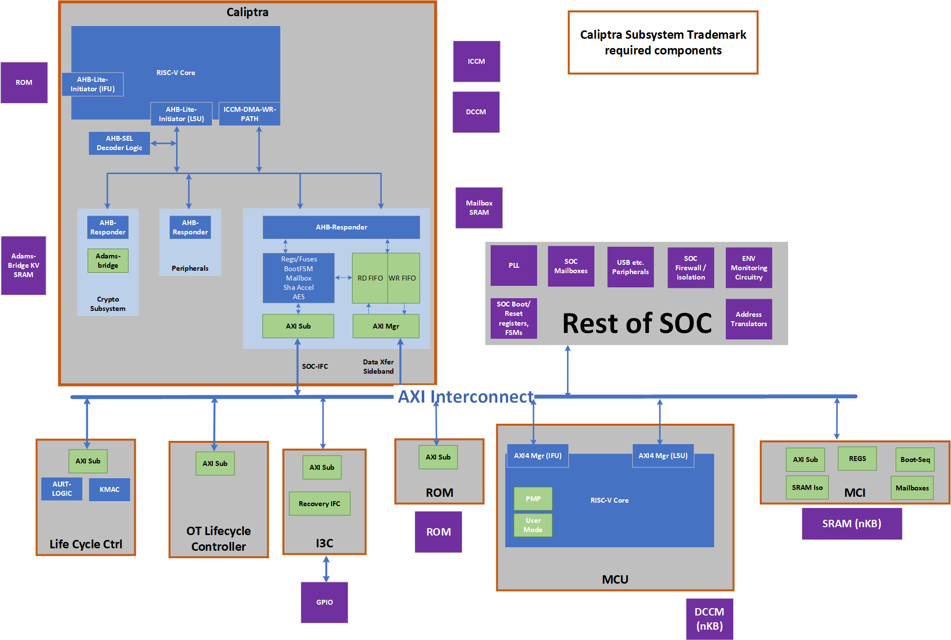
Caliptra Subsystem includes:
- Caliptra Core: The Caliptra Core IP. For more information, see Caliptra: A Datacenter System on a Chip (SoC) Root of Trust (RoT).
- MCU (Manufacturer Control Unit): A microcontroller unit that manages various control tasks within the subsystem.
- I3C Core: An interface for connecting and communicating with I3C devices, which are used for providing streaming boot support and communicating with other I3C host controllers.
- Life Cycle Controller: A component that manages the different stages of the subsystem's lifecycle, including initialization, operation, and shutdown.
- Fuse Controller (OTP): A one-time programmable memory controller used for storing critical configuration data and security keys.
- MCI (Manufacturer Control Interface (for MCU)): Manages the communication between the processor and the memory components.
- Memories: Various memory components used for storing data and instructions required by the subsystem.
Integration Considerations
By performing these design and verification tasks, the integrator ensures that the Caliptra Subsystem is properly integrated and can function as intended within the larger system. Several files contain code that may be specific to an integrator's implementation and should be overridden. This overridable code is either configuration parameters with integrator-specific values or modules that implement process-specific functionality. Code in these files should be modified or replaced by integrators using components from the cell library of their fabrication vendor. The following table describes recommended modifications for each file.
| File | Description |
|---|---|
| css_mcu0_dmi_jtag_to_core_sync.v | Replace with a technology-specific sync cell. This synchronizer implements edge detection logic using a delayed flip flop on the output domain to produce a pulse output. Integrators must take care to ensure logical equivalence when replacing this logic with custom cells. |
| css_mcu0_beh_lib.sv | Replace css_mcu0_rvclkhdr/css_mcu0_rvoclkhdr with a technology-specific clock gater. Modifying this file may not be necessary if integrators override the clock gate module that is used by setting TECH_SPECIFIC_EC_RV_ICG. |
| css_mcu0_beh_lib.sv | Replace css_mcu0_rvsyncss (and css_mcu0_rvsyncss_fpga if the design will be implemented on an FPGA) with a technology-specific sync cell. |
| src/integration/rtl/caliptra_ss_includes.svh | Modify the parameter CPTRA_SS_ROM_SIZE_KB to define the correct size of the MCU ROM in integrated design. No other parameters in this file are permitted to be modified. |
Caliptra Core RTL modifications
It is mandatory that any build processes used (e.g. simulation, lint, synthesis) define the Verilog macro CALIPTRA_MODE_SUBSYSTEM, as described in the Caliptra Core Integration Specification. This ensures that Caliptra provides all Subsystem-related features and configuration. Example build scripts provided in the Caliptra Subsystem repository (such as Makefile) demonstrate how this might be performed.
Design Considerations
- Replace the AXI Interconnect: The subsystem utilizes an AXI-based interconnect to facilitate communication between components, with the Caliptra core connecting via an AXI interface. The integrator must replace the default AXI interconnect component with their proprietary interface. This ensures that the subsystem can communicate effectively with the rest of the subsystem components using the integrator's specific interconnect architecture.
- Connect the Memories: The integrator must connect the various memory components required by the subsystem. These memory components are used for storing data and instructions necessary for the operation of the Caliptra subsystem.
- No Changes to Internals: Integrators are not expected to make any changes to the internals of the design. The focus should be on ensuring proper integration and connectivity of the subsystem components.
Verification Considerations
- Connect the I3C Core GPIO with I3C host driver: The integrator must connect the I3C core (two target I3C devices) to the appropriate driver for the GPIO pins. This connection is crucial for enabling communication with I3C devices, which are used for communication within the subsystem.
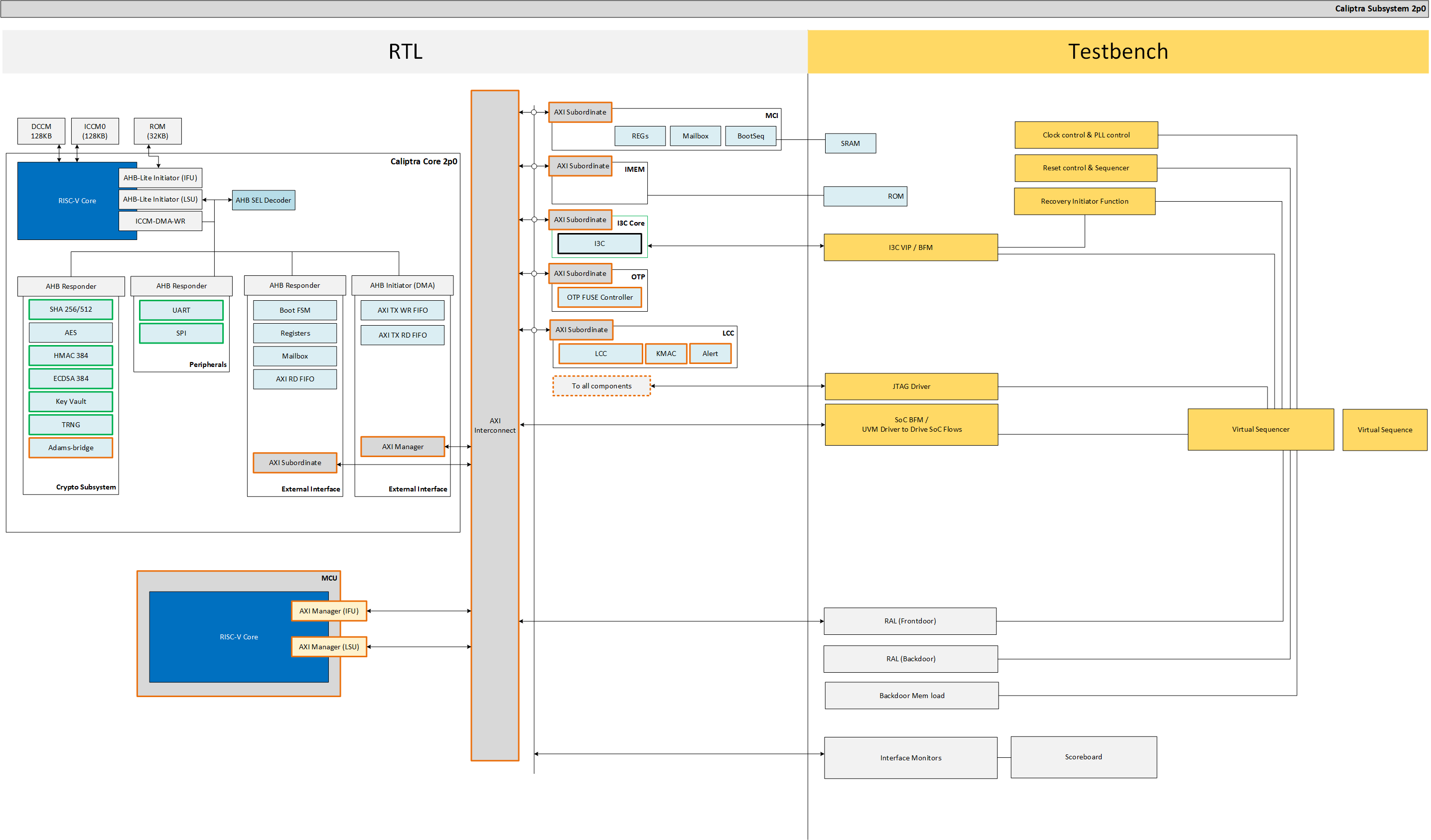
Verification View of Caliptra Subsystem
The following block diagram shows details on verification view of Caliptra Subsystem
Memory Requirements
Integrators must instantiate SRAM components outside of the Caliptra Subsystem boundary (see SRAM Implementation for more details). SRAM wrapper logic within the Caliptra Subsystem boundary facilitates the connection to SRAM instances through memory export interfaces in the top-level port list. Integrators must connect the following memory export interfaces to the instantiated SRAM components.
SoC Specific in below table means the size of the memory is not fixed and can be configured based on the design requirements by integrator. The actual size will depend on the specific implementation and configuration of the Caliptra Subsystem.
| Device | Memory Name | Interface | Size | Access Type | Description |
|---|---|---|---|---|---|
| MCU0 | Instruction ROM | mcu_rom_mem_export_if | SoC Specific | Read-Only | Stores the instructions for MCU0 execution. Write-enable (we) and write-data (wdata) signals must be left unconnected, as MCU ROM has no write support. |
| MCU0 | Memory Export | cptra_ss_mcu0_el2_mem_export | SoC Specific | Read/Write | Memory export for MCU0 access |
| MCU0 | Shared Memory (SRAM) | cptra_ss_mci_mcu_sram_req_if | SoC Specific | Read/Write | Shared memory between MCI and MCU for data storage |
| MAILBOX | MBOX0 Memory | cptra_ss_mci_mbox0_sram_req_if | SoC Specific | Read/Write | Memory for MBOX0 communication |
| MAILBOX | MBOX1 Memory | cptra_ss_mci_mbox1_sram_req_if | SoC Specific | Read/Write | Memory for MBOX1 communication |
| Caliptra Core | ICCM, DCCM | cptra_ss_cptra_core_el2_mem_export | Refer to Caliptra Core spec | Read/Write | Interface for the Instruction and Data Closely Coupled Memory (ICCM, DCCM) of the core |
| Caliptra Core | Caliptra ROM | cptra_ss_cptra_core_imem | Refer to Caliptra Core spec | Read-Only | Interface for Caliptra ROM |
| Caliptra Core | Caliptra Mailbox SRAM | cptra_ss_cptra_core_mbox_sram | Refer to Caliptra Core spec | Read/Write | Interface for Caliptra mailbox memory |
| Caliptra Core | Caliptra MLDSA SRAM | mldsa_memory_export_req | Refer to Caliptra Core spec | Read/Write | Interface for SRAM instantiated within Adams Bridge block |
Caliptra Subsystem Top
The integration of the Caliptra Subsystem begins with the instantiation of the top-level RTL module, caliptra_ss_top.sv. This module serves as the primary entry point for the subsystem and encapsulates all the logic and components required for the functionality of the Caliptra Root of Trust (RoT). All signals must be connected based on the detailed interface and signal descriptions provided in this document. Ensure adherence to the signal direction, width, and functionality to guarantee proper integration with the host SoC.
Parameters & Defines
File at this path in the repository includes parameters and defines for Caliptra Subsystem src/integration/rtl/caliptra_ss_includes.svh
Interfaces & Signals
IMPORTANT NOTE: All signals assumed to by synchronous to cptra_ss_clk_i.
Table: Caliptra SS Straps
| Facing | Type | width | Name | Description |
|---|---|---|---|---|
| External | input | 32 | cptra_ss_strap_mcu_lsu_axi_user_i | MCU LSU AXI user strap input |
| External | input | 32 | cptra_ss_strap_mcu_ifu_axi_user_i | MCU IFU AXI user strap input |
| External | input | 32 | cptra_ss_strap_mcu_sram_config_axi_user_i | MCU SRAM Configuration AXI user strap input. |
| External | input | 32 | cptra_ss_strap_mci_soc_config_axi_user_i | MCI SOC Configuration AXI user strap input |
| External | input | 32 | cptra_ss_strap_caliptra_dma_axi_user_i | Caliptra DMA AXI user strap input |
| External | input | 32 | cptra_ss_strap_mcu_reset_vector_i | MCU reset vector strap input |
| External | input | 64 | cptra_ss_strap_caliptra_base_addr_i | Caliptra base address strap input |
| External | input | 64 | cptra_ss_strap_mci_base_addr_i | MCI base address strap input |
| External | input | 64 | cptra_ss_strap_recovery_ifc_base_addr_i | Recovery interface base address strap input |
| External | input | 64 | cptra_ss_strap_otp_fc_base_addr_i | OTP FC base address strap input |
| External | input | 64 | cptra_ss_strap_uds_seed_base_addr_i | UDS seed base address strap input |
| External | input | 32 | cptra_ss_strap_prod_debug_unlock_auth_pk_hash_reg_bank_offset_i | Prod debug unlock auth PK hash reg bank offset input |
| External | input | 32 | cptra_ss_strap_num_of_prod_debug_unlock_auth_pk_hashes_i | Number of prod debug unlock auth PK hashes input |
| External | input | 32 | cptra_ss_strap_generic_0_i | Provides the Caliptra ROM with a 32-bit pointer that encodes the location of the fuse controller's status register and the bit position of the idle indicator. Upper 16 bits: Bit index of the IDLE_BIT_STATUS within SOC_OTP_CTRL_STATUS. Lower 16 bits: Offset address of SOC_OTP_CTRL_STATUS within the SOC_IFC_REG space, relative to SOC_OTP_CTRL_BASE_ADDR. |
| External | input | 32 | cptra_ss_strap_generic_1_i | Provides the Caliptra ROM with a 32-bit pointer to the fuse controller’s command register (CMD), enabling ROM-level control or triggering of fuse operations. |
| External | input | 32 | cptra_ss_strap_generic_2_i | Generic strap input 2 |
| External | input | 32 | cptra_ss_strap_generic_3_i | Generic strap input 3 |
| External | input | 1 | cptra_ss_debug_intent_i | Physical presence bit required to initiate the debug unlock flow. For more details, refer to the Production Debug Unlock Flow and How does Caliptra Subsystem enable manufacturing debug mode?. For SOCs that choose to use these features, this port should be connected to a GPIO |
AXI Interface (axi_if)
| Signal | Width | Direction (mgr) | Direction (sub) |
|---|---|---|---|
araddr | AW | output | input |
arburst | $bits(axi_burst_e) | output | input |
arsize | 3 | output | input |
arlen | 8 | output | input |
aruser | UW | output | input |
arid | IW | output | input |
arlock | 1 | output | input |
arvalid | 1 | output | input |
arready | 1 | input | output |
rdata | DW | input | output |
rresp | $bits(axi_resp_e) | input | output |
rid | IW | input | output |
rlast | 1 | input | output |
rvalid | 1 | input | output |
rready | 1 | output | input |
awaddr | AW | output | input |
awburst | $bits(axi_burst_e) | output | input |
awsize | 3 | output | input |
awlen | 8 | output | input |
awuser | UW | output | input |
awid | IW | output | input |
awlock | 1 | output | input |
awvalid | 1 | output | input |
awready | 1 | input | output |
wdata | DW | output | input |
wstrb | DW/8 | output | input |
wvalid | 1 | output | input |
wready | 1 | input | output |
wlast | 1 | output | input |
bresp | $bits(axi_resp_e) | input | output |
bid | IW | input | output |
bvalid | 1 | input | output |
bready | 1 | output | input |
Caliptra Subsystem Top Interface & Signals
| Facing | Type | width | Signal or Interface Name | Description |
|---|---|---|---|---|
| External | input | 1 | cptra_ss_clk_i | Caliptra subsystem clock input |
| External | input | 1 | cptra_ss_pwrgood_i | Power good signal input |
| External | input | 1 | cptra_ss_rst_b_i | Reset signal input, active low |
| External | input | 1 | cptra_ss_mci_cptra_rst_b_i | Reset signal input for Caliptra Core, active low. See Caliptra Core Reset Control for more details |
| External | output | 1 | cptra_ss_mci_cptra_rst_b_o | Reset signal output from MCI for Caliptra Core, active low. See Caliptra Core Reset Control for more details |
| External | input | 1 | cptra_ss_mcu_rst_b_i | Reset signal input for MCU, active low. See MCU Reset Control for more details |
| External | output | 1 | cptra_ss_mcu_rst_b_o | Reset signal output for MCU, active low. See MCU Reset Control for more details |
| External | output | 1 | cptra_ss_warm_reset_rdc_clk_dis_o | Clock disable for warm reset. Used to disable cptra_ss_rdc_clk_cg_o and cptra_ss_mcu_clk_cg_o clocks. Asserted a few clock cycles after cptra_ss_rst_b_i asserted and before cptra_ss_rst_b_o asserted. Deasserted a few clock cycles after cptra_ss_rst_b_i deasserted. |
| External | output | 1 | cptra_ss_early_warm_reset_warn_o | Early reset warn used to change security related signals to a safe value before reset is asserted. Needed since Caliptra Core clock gating is slightly after MCI clock gating/reset assertion. Example is the security_state fed from MCI to Caliptra Core. |
| External | output | 1 | cptra_ss_mcu_fw_update_rdc_clk_dis_o | Clock disable for MCU reset. Used to disable cptra_ss_mcu_clk_cg_o clock. Asserted a few clock cycles before cptra_ss_mcu_rst_b_o is asserted. Deasserted when MCI boot sequencer switches out of BOOT_RST_MCU state. |
| External | output | 1 | cptra_ss_rdc_clk_cg_o | Caliptra subsystem clock gated clock for RDC. Clock Control |
| External | output | 1 | cptra_ss_mcu_clk_cg_o | MCU clock gated clock for RDC. Clock Control |
| External | output | 1 | cptra_ss_rst_b_o | Caliptra subsystem reset aligned for RDC crossing Reset Control |
| External | axi_if | na | cptra_ss_cptra_core_s_axi_if_w_sub | Caliptra core AXI write sub-interface |
| External | axi_if | na | cptra_ss_cptra_core_s_axi_if_r_sub | Caliptra core AXI read sub-interface |
| External | axi_if | na | cptra_ss_cptra_core_m_axi_if_w_mgr | Caliptra core AXI write manager interface |
| External | axi_if | na | cptra_ss_cptra_core_m_axi_if_r_mgr | Caliptra core AXI read manager interface |
| External | axi_if | na | cptra_ss_mci_s_axi_if_w_sub | Caliptra Subsystem MCI AXI write sub-interface |
| External | axi_if | na | cptra_ss_mci_s_axi_if_r_sub | Caliptra Subsystem MCI AXI read sub-interface |
| External | axi_if | na | cptra_ss_mcu_rom_s_axi_if_w_sub | Caliptra Subsystem MCU ROM AXI write sub-interface. Writes to MCU ROM are not supported, this interface shall be left unconnected from AXI interconnect and tied to 0-value inputs. |
| External | axi_if | na | cptra_ss_mcu_rom_s_axi_if_r_sub | Caliptra Subsystem MCU ROM AXI read sub-interface |
| External | axi_if | na | cptra_ss_mcu_lsu_m_axi_if_w_mgr | Caliptra Subsystem MCU LSU AXI write manager interface |
| External | Output | 4 | cptra_ss_mcu_lsu_m_axi_if_awcache | Caliptra Subsystem MCU LSU AXI write manager address transaction attributes signal |
| External | Output | 3 | cptra_ss_mcu_lsu_m_axi_if_awprot | Caliptra Subsystem MCU LSU AXI write manager address protection type signal |
| External | Output | 4 | cptra_ss_mcu_lsu_m_axi_if_awregion | Caliptra Subsystem MCU LSU AXI write manager address region identifier signal |
| External | Output | 4 | cptra_ss_mcu_lsu_m_axi_if_awqos | Caliptra Subsystem MCU LSU AXI write manager address quality of service signal |
| External | axi_if | na | cptra_ss_mcu_lsu_m_axi_if_r_mgr | Caliptra Subsystem MCU LSU AXI read manager interface |
| External | Output | 4 | cptra_ss_mcu_lsu_m_axi_if_arcache | Caliptra Subsystem MCU LSU AXI read manager address transaction attributes signal |
| External | Output | 3 | cptra_ss_mcu_lsu_m_axi_if_arprot | Caliptra Subsystem MCU LSU AXI read manager address protection type signal |
| External | Output | 4 | cptra_ss_mcu_lsu_m_axi_if_arregion | Caliptra Subsystem MCU LSU AXI read manager address region identifier signal |
| External | Output | 4 | cptra_ss_mcu_lsu_m_axi_if_arqos | Caliptra Subsystem MCU LSU AXI read manager address quality of service signal |
| External | axi_if | na | cptra_ss_mcu_ifu_m_axi_if_w_mgr | Caliptra Subsystem MCU IFU AXI write manager interface |
| External | Output | 4 | cptra_ss_mcu_ifu_m_axi_if_awcache | Caliptra Subsystem MCU IFU AXI write manager address transaction attributes signal |
| External | Output | 3 | cptra_ss_mcu_ifu_m_axi_if_awprot | Caliptra Subsystem MCU IFU AXI write manager address protection type signal |
| External | Output | 4 | cptra_ss_mcu_ifu_m_axi_if_awregion | Caliptra Subsystem MCU IFU AXI write manager address region identifier signal |
| External | Output | 4 | cptra_ss_mcu_ifu_m_axi_if_awqos | Caliptra Subsystem MCU IFU AXI write manager address quality of service signal |
| External | axi_if | na | cptra_ss_mcu_ifu_m_axi_if_r_mgr | Caliptra Subsystem MCU IFU AXI read manager interface |
| External | Output | 4 | cptra_ss_mcu_ifu_m_axi_if_arcache | Caliptra Subsystem MCU IFU AXI read manager address transaction attributes signal |
| External | Output | 3 | cptra_ss_mcu_ifu_m_axi_if_arprot | Caliptra Subsystem MCU IFU AXI read manager address protection type signal |
| External | Output | 4 | cptra_ss_mcu_ifu_m_axi_if_arregion | Caliptra Subsystem MCU IFU AXI read manager address region identifier signal |
| External | Output | 4 | cptra_ss_mcu_ifu_m_axi_if_arqos | Caliptra Subsystem MCU IFU AXI read manager address quality of service signal |
| External | axi_if | na | cptra_ss_mcu_sb_m_axi_if_w_mgr | Caliptra Subsystem MCU System Bus AXI write manager interface |
| External | Output | 4 | cptra_ss_mcu_sb_m_axi_if_awcache | Caliptra Subsystem MCU System Bus AXI write manager address transaction attributes signal |
| External | Output | 3 | cptra_ss_mcu_sb_m_axi_if_awprot | Caliptra Subsystem MCU System Bus AXI write manager address protection type signal |
| External | Output | 4 | cptra_ss_mcu_sb_m_axi_if_awregion | Caliptra Subsystem MCU System Bus AXI write manager address region identifier signal |
| External | Output | 4 | cptra_ss_mcu_sb_m_axi_if_awqos | Caliptra Subsystem MCU System Bus AXI write manager address quality of service signal |
| External | axi_if | na | cptra_ss_mcu_sb_m_axi_if_r_mgr | Caliptra Subsystem MCU System Bus AXI read manager interface |
| External | Output | 4 | cptra_ss_mcu_sb_m_axi_if_arcache | Caliptra Subsystem MCU System Bus AXI read manager address transaction attributes signal |
| External | Output | 3 | cptra_ss_mcu_sb_m_axi_if_arprot | Caliptra Subsystem MCU System Bus AXI read manager address protection type signal |
| External | Output | 4 | cptra_ss_mcu_sb_m_axi_if_arregion | Caliptra Subsystem MCU System Bus AXI read manager address region identifier signal |
| External | Output | 4 | cptra_ss_mcu_sb_m_axi_if_arqos | Caliptra Subsystem MCU System Bus AXI read manager address quality of service signal |
| External | axi_if | na | cptra_ss_i3c_s_axi_if_w_sub | Caliptra Subsystem I3C AXI write sub-interface |
| External | axi_if | na | cptra_ss_i3c_s_axi_if_r_sub | Caliptra Subsystem I3C AXI read sub-interface |
| External | input | na | cptra_ss_lc_axi_wr_req_i | LC controller AXI write request input |
| External | output | na | cptra_ss_lc_axi_wr_rsp_o | LC controller AXI write response output |
| External | input | na | cptra_ss_lc_axi_rd_req_i | LC controller AXI read request input |
| External | output | na | cptra_ss_lc_axi_rd_rsp_o | LC controller AXI read response output |
| External | input | 128 | cptra_ss_raw_unlock_token_hashed_i | Hashed token for RAW unlock |
| External | input | na | cptra_ss_otp_core_axi_wr_req_i | OTP controller AXI write request input |
| External | output | na | cptra_ss_otp_core_axi_wr_rsp_o | OTP controller AXI write response output |
| External | input | na | cptra_ss_otp_core_axi_rd_req_i | OTP controller AXI read request input |
| External | output | na | cptra_ss_otp_core_axi_rd_rsp_o | OTP controller AXI read response output |
| External | input | 256 | cptra_ss_cptra_obf_key_i | Caliptra core obfuscation key input |
| External | input | CLP_CSR_HMAC_KEY_DWORDS | cptra_ss_cptra_csr_hmac_key_i | Caliptra core CSR HMAC key input |
| External | input | 1 | cptra_ss_cptra_core_jtag_tck_i | JTAG clock input |
| External | input | 1 | cptra_ss_cptra_core_jtag_tms_i | JTAG TMS input |
| External | input | 1 | cptra_ss_cptra_core_jtag_tdi_i | JTAG TDI input |
| External | input | 1 | cptra_ss_cptra_core_jtag_trst_n_i | JTAG reset input, active low |
| External | output | 1 | cptra_ss_cptra_core_jtag_tdo_o | JTAG TDO output |
| External | output | 1 | cptra_ss_cptra_core_jtag_tdoEn_o | JTAG TDO enable output |
| External | output | 125 | cptra_ss_cptra_generic_fw_exec_ctrl_o | Generic firmware execution control output |
| External | output | 1 | cptra_ss_cptra_generic_fw_exec_ctrl_2_mcu_o | Generic firmware execution control bit 2 from Caliptra output |
| External | input | 1 | cptra_ss_cptra_generic_fw_exec_ctrl_2_mcu_i | Generic firmware execution control bit 2 for MCU input |
| External | output | 1 | cptra_ss_all_error_fatal_o | Caliptra SS fatal error |
| External | output | 1 | cptra_ss_all_error_non_fatal_o | Caliptra SS non-fatal error |
| External | input | na | cptra_ss_lc_ctrl_jtag_i | LC controller JTAG request input |
| External | output | na | cptra_ss_lc_ctrl_jtag_o | LC controller JTAG response output |
| External | interface | na | cptra_ss_cptra_core_el2_mem_export | Caliptra core EL2 memory export interface |
| External | interface | na | mcu_rom_mem_export_if | MCU ROM memory export interface. Write-enable (we) and write-data (wdata) signals must be left unconnected, as MCU ROM has no write support. |
| External | output | 1 | cptra_ss_cptra_core_mbox_sram_cs_o | Mailbox SRAM chip select output |
| External | output | 1 | cptra_ss_cptra_core_mbox_sram_we_o | Mailbox SRAM write enable output |
| External | output | CPTRA_MBOX_ADDR_W | cptra_ss_cptra_core_mbox_sram_addr_o | Mailbox SRAM address output |
| External | output | CPTRA_MBOX_DATA_AND_ECC_W | cptra_ss_cptra_core_mbox_sram_wdata_o | Mailbox SRAM write data output |
| External | input | CPTRA_MBOX_DATA_AND_ECC_W | cptra_ss_cptra_core_mbox_sram_rdata_i | Mailbox SRAM read data input |
| External | output | 1 | cptra_ss_cptra_core_imem_cs_o | Instruction memory chip select output |
| External | output | CALIPTRA_IMEM_ADDR_WIDTH | cptra_ss_cptra_core_imem_addr_o | Instruction memory address output |
| External | input | CALIPTRA_IMEM_DATA_WIDTH | cptra_ss_cptra_core_imem_rdata_i | Instruction memory read data input |
| External | input | 1 | cptra_ss_cptra_core_bootfsm_bp_i | Boot FSM breakpoint input |
| External | output | 1 | cptra_ss_cptra_core_etrng_req_o | External TRNG request output |
| External | input | 4 | cptra_ss_cptra_core_itrng_data_i | Internal TRNG data input |
| External | input | 1 | cptra_ss_cptra_core_itrng_valid_i | Internal TRNG valid input |
| External | interface | na | cptra_ss_mci_mcu_sram_req_if | MCI MCU SRAM request interface |
| External | interface | na | cptra_ss_mci_mbox0_sram_req_if | MCI mailbox 0 SRAM request interface |
| External | interface | na | cptra_ss_mci_mbox1_sram_req_if | MCI mailbox 1 SRAM request interface |
| External | output | 1 | cptra_ss_soc_mcu_mbox0_data_avail | MCU Mailbox0 data available output |
| External | output | 1 | cptra_ss_soc_mcu_mbox1_data_avail | MCU Mailbox1 data available output |
| External | interface | na | cptra_ss_mcu0_el2_mem_export | MCU0 EL2 memory export interface |
| External | input | 64 | cptra_ss_mci_generic_input_wires_i | Generic input wires for MCI |
| External | input | 1 | cptra_ss_mcu_no_rom_config_i | No ROM configuration input |
| External | input | 1 | cptra_ss_mci_boot_seq_brkpoint_i | MCI boot sequence breakpoint input |
| External | input | 1 | cptra_ss_lc_Allow_RMA_or_SCRAP_on_PPD_i | Allow RMA or SCRAP on PPD input |
| External | input | 1 | cptra_ss_FIPS_ZEROIZATION_PPD_i | Zeroization request with PPD input. If FIPS zeroization flow is required, it shall be set before Caliptra SS is out of reset. |
| External | output | 1 | cptra_ss_dbg_manuf_enable_o | Indication that the debug is unlocked for manufacturing state and this is set by Caliptra Core |
| External | output | 64 | cptra_ss_cptra_core_soc_prod_dbg_unlock_level_o | Indication that the debug is unlocked for production state. Each bit represents a debug level. Currently, 8-bit is supported with Caliptra ROM |
| External | output | na | caliptra_ss_life_cycle_steady_state_o | Life-cycle state broadcasted by fuse macro for any additional SOC specific use cases |
| External | output | 1 | caliptra_ss_otp_state_valid_o | One-bit valid indicator for the broadcast life-cycle state (caliptra_ss_life_cycle_steady_state_o). |
| External | output | 1 | caliptra_ss_volatile_raw_unlock_success_o | Asserted when the life-cycle controller grants the volatile-unlock state and remains asserted until the next power-cycle. This transition bypasses the fuse macro, so caliptra_ss_life_cycle_steady_state_o and caliptra_ss_otp_state_valid_o do not reflect it. |
| External | output | 64 | cptra_ss_mci_generic_output_wires_o | Generic output wires for MCI |
| External | input | 1 | cptra_ss_mcu_jtag_tck_i | MCU JTAG clock input |
| External | input | 1 | cptra_ss_mcu_jtag_tms_i | MCU JTAG TMS input |
| External | input | 1 | cptra_ss_mcu_jtag_tdi_i | MCU JTAG TDI input |
| External | input | 1 | cptra_ss_mcu_jtag_trst_n_i | MCU JTAG reset input, active low |
| External | output | 1 | cptra_ss_mcu_jtag_tdo_o | MCU JTAG TDO output |
| External | output | 1 | cptra_ss_mcu_jtag_tdoEn_o | MCU JTAG TDO enable output |
| External | input | 1 | cptra_ss_i3c_scl_i | I3C clock input |
| External | input | 1 | cptra_ss_i3c_sda_i | I3C data input |
| External | output | 1 | cptra_ss_i3c_scl_o | I3C clock output |
| External | output | 1 | cptra_ss_i3c_sda_o | I3C data output |
| External | output | 1 | cptra_ss_i3c_scl_oe | I3C clock output enable |
| External | output | 1 | cptra_ss_i3c_sda_oe | I3C data output enable |
| External | input | 1 | cptra_i3c_axi_user_id_filtering_enable_i | I3C AXI user filtering enable (active high) |
| External | output | 1 | cptra_ss_sel_od_pp_o | Select open-drain push-pull output |
| External | output | 1 | cptra_ss_i3c_recovery_payload_available_o | I3C indicates recovery payload is available. If there is no external I3C it should be looped back to cptra_ss_i3c_recovery_payload_available_i. If there is an external I3C it can be combined with or replaced with SOC logic and connected to cptra_ss_i3c_recovery_payload_available_i |
| External | input | 1 | cptra_ss_i3c_recovery_payload_available_i | I3C indication for Caliptra Core that a recovery payload is available. If no external I3C should be connected to cptra_ss_i3c_recovery_payload_available_o. If external I3C it can be connected to a combination of SOC logic + cptra_ss_i3c_recovery_payload_available_o |
| External | output | 1 | cptra_ss_i3c_recovery_image_activated_o | Indicates the recovery image is activated. If there is no external I3C it should be looped back to cptra_ss_i3c_recovery_image_activated_i. If there is an external I3C it can be combined with or replaced with SOC logic and connected to cptra_ss_i3c_recovery_image_activated_i |
| External | input | 1 | cptra_ss_i3c_recovery_image_activated_i | I3C indication for Caliptra Core that the recovery image is activated. If no external I3C should be connected to cptra_ss_i3c_recovery_image_activated_o. If there is an external I3C it can be connected to a combination of SOC logic + cptra_ss_i3c_recovery_image_activated_o |
| External | input | 64 | cptra_ss_cptra_core_generic_input_wires_i | Generic input wires for Caliptra core |
| External | input | 1 | cptra_ss_cptra_core_scan_mode_i | Caliptra core scan mode input |
| External | output | 1 | cptra_error_fatal | Fatal error output |
| External | output | 1 | cptra_error_non_fatal | Non-fatal error output |
| External | output | 1 | cptra_ss_mcu_halt_status_o | MCU halt status |
| External | output | 1 | cptra_ss_mcu_halt_status_i | MCU halt status input used by MCI |
| External | output | 1 | cptra_ss_mcu_halt_ack_o | MCU halt ack |
| External | output | 1 | cptra_ss_mcu_halt_ack_i | MCU halt ack input used by MCI |
| External | output | 1 | cptra_ss_mcu_halt_req_o | MCU halt request |
Integration Requirements
Clock
The cptra_ss_clk_i signal is the primary clock input for the Caliptra Subsystem.
- Signal Name
cptra_ss_clk_i - Required Frequency 333* MHz to 400 MHz
- I3C core imposes requirement for minimum operating clock frequency set to 333 MHz or higher to meet 12ns tSCO timing.
- SoCs that run Caliptra lower than 333 MHz will limit the max I3C SCL frequency. See I3C Phy Spec for more details.
- This was changed from 170 MHz floor due to CDC issue found in I3C core:
- Clock Source Must be derived from the SoC’s clock generation module or a stable external oscillator.
- Integration Notes
- Verify that the SoC or system-level clock source provides a stable clock.
- The clock signal must be properly buffered if necessary to meet the subsystem's setup and hold timing requirements.
- If a different frequency is required, ensure that a clock divider or PLL is used to generate clock before connection.
The cptra_ss_rdc_clk_cg_o output clock is a clock gated version of cptra_ss_clk_i. It is clock gated whenever cptra_ss_rst_b is asserted to avoid RDC issues from the warm reset domain to the cold reset domain/memories.
- Signal Name
cptra_ss_rdc_clk_cg_o - Required Frequency Same as
cptra_ss_clk_i. - Clock Source Caliptra SS MCI clock gater
- Integration Notes
- Gated a few clock cycles before
cptra_ss_rst_b_oasserted and remains gated until reset is deasserted. - MCU SRAM and MCU MBOX memories shall be connected to this clock to avoid RDC issues.
- Clock gating controlled by
cptra_ss_warm_reset_rdc_clk_dis_o. - Any SOC logic on a deeper reset domain than CSS can use this clock to resolve RDC issues.
- Gated a few clock cycles before
The cptra_ss_mcu_clk_cg_o output clock is a gated version of cptra_ss_clk_i. It is gated whenever cptra_ss_mcu_rst_b_o is asserted to avoid RDC issues within the MCU warm and cold reset domains.
- Signal Name
cptra_ss_mcu_clk_cg_o - Required Frequency Same as
cptra_ss_clk_i. - Clock Source Caliptra SS MCI clock gater
- Integration Notes
- Gated a few clock cycles before
cptra_ss_mcu_rst_b_oasserted and remains gated until reset is deasserted. - Clock gating controlled by
cptra_ss_mcu_fw_update_rdc_clk_dis_oandcptra_ss_warm_reset_rdc_clk_dis_o. - Any SOC logic on a deeper reset domain than MCU can use this clock to resolve RDC issues.
- Gated a few clock cycles before
Reset
The cptra_ss_rst_b_i signal is the primary reset input for the Caliptra Subsystem. It must be asserted low to reset the subsystem and de-asserted high to release it from reset. Ensure that the reset is held low for a sufficient duration (minimum of 2 clock cycles) to allow all internal logic to initialize properly.
- Signal Name
cptra_ss_rst_b_i - Active Level Active-low (
0resets the subsystem,1releases reset) - Reset Type Synchronous with the
cptra_ss_clk_isignal - Integration Notes
- The reset signal must be synchronized to the
cptra_ss_clk_iclock to prevent metastability issues. - If the reset source is asynchronous, a synchronizer circuit must be used before connecting to the subsystem.
- During SoC initialization, assert this reset signal until all subsystem clocks and required power domains are stable.
- It is illegal to only toggle
cptra_ss_rst_b_iuntil both Caliptra and MCU have received at least one FW update. Failure to follow this requirement could cause them to execute out of an uninitialized SRAM. - SOC should assert
cptra_ss_reset_b_iaftercptra_ss_mcu_halt_status_ois asserted to guarantee MCU is idle. This will guarantee no outstanding AXI transactions from MCU and help avoid RDC issues.
- The reset signal must be synchronized to the
The cptra_ss_rst_b_o is a delayed version of cptra_ss_rst_b_i to ensure cptra_ss_rdc_clk_cg_o is gated before reset is asserted. This reset is needed for the purpose of RDC between the warm reset domain and the cold reset/memory domain.
- Signal Name
cptra_ss_rst_b_o - Active Level Active-low (
0resets the subsystem,1releases reset) - Reset Type Synchronous with the
cptra_ss_rdc_clk_cg_osignal - Integration Notes
- SOCs shall use this reset for any memory logic connected to MCU SRAM or MCU MBOX to avoid RDC corruption of the memories.
- It is recommended to be used for SOC AXI interconnect if it is on the same reset domain as Caliptra SS to avoid RDC issues.
- SOC logic on
cptra_ss_rst_b_idomain and transitions into a deeper reset domain can use this reset paired withcptra_ss_rdc_clk_cg_oto avoid RDC issues.
Power Good Signal
The cptra_ss_pwrgood_i signal serves as an indicator of stable power for the Caliptra Subsystem. When asserted (1), it confirms that power is stable and the subsystem can operate normally. When deasserted (0), the signal triggers a hard reset of the subsystem. Deassertion must be synchronized to cptra_ss_clk_i to avoid metastability issues.
- Signal Name
cptra_ss_pwrgood_i - Active Level Active-high (
1indicates stable power,0triggers reset) - Assertion Type Asynchronous
- Deassertion Type Synchronous to
cptra_ss_clk_i - Integration Notes
- Ensure
cptra_ss_pwrgood_iis properly generated by the power management unit or system power controller. - Since assertion is asynchronous, it must be immediately driven high once power is stable.
- Use a synchronizer to properly align deassertion with
cptra_ss_clk_ito prevent glitches. - If
cptra_ss_pwrgood_iremains low, the Caliptra Subsystem will remain in a hard reset state.
- Ensure
Connecting AXI Interconnect
Integrator must connect following list of manager and subordinates to axi interconnect.
- List of AXI Manager connections to AXI interconnect.
| Manager AXI If Name | Description |
|---|---|
cptra_ss_mcu_lsu_m_axi_if | Manager interface for MCU Load/Store Unit (LSU). All additional AXI signals present in the top-level port list that are not part of the axi_if interface must also be connected to the AXI interconnect (AxCACHE, AxPROT, AxREGION, AxQOS). |
cptra_ss_mcu_ifu_m_axi_if | Manager interface for MCU Instruction Fetch Unit (IFU). All additional AXI signals present in the top-level port list that are not part of the axi_if interface must also be connected to the AXI interconnect (AxCACHE, AxPROT, AxREGION, AxQOS). |
cptra_ss_mcu_sb_m_axi_if | Manager interface for MCU System Bus (SB). Used for debug only. All additional AXI signals present in the top-level port list that are not part of the axi_if interface must also be connected to the AXI interconnect (AxCACHE, AxPROT, AxREGION, AxQOS). |
cptra_ss_cptra_core_m_axi_if | Manager interface for the Caliptra Core AXI transactions. Additional signals are unused and may be tied to 0 at the interconnect (AxCACHE, AxPROT, AxREGION, AxQOS). |
-
AXI USER width is 32-bits for all AXI interfaces in the Caliptra Subsystem. Only the Address User signals are used (ARUSER and AWUSER) for secure access filtering. Other USER signals are either tied to 0 or not used (WUSER, RUSER, BUSER). ARUSER and AWUSER must be passed unmodified through the AXI interconnect to all AXI subordinates in the Subsystem. Each logic block inside the Subsystem is responsible for performing its own AXI User filtering based on access privileges. AXI interconnect is only responsible for passing the unmodified signals along with the transaction requests, not for performing any access filtering.
-
AXI ID width at each MCU manager interface must not be modified from the configured values. ID width for each of the MCU AXI Manager interfaces is defined by the <IF_NAME>_BUS_TAG parameter from this file: css_mcu0_el2_param.vh. Port connections may be seen in mcu_top.sv. ID Width of the Caliptra DMA AXI Manager interface is defined in soc_ifc_pkg.sv.
- IFU_BUS_TAG: 3. Interconnect should support ID values 0-7.
- LSU_BUS_TAG: 3. Interconnect should support ID values 0-7.
- SB_BUS_TAG: 1. Interconnect should support ID values 0,1.
- CPTRA_AXI_DMA_ID_WIDTH: 5. ID signals are tied to constant 0.
-
For each AXI subordinate interface in the Subsystem the following table shows ID WIDTH default value, file to review for the configured definition, and any support for configurability. | Interface | Default ID WIDTH | Reference File | Description | | ----------- | ------------------ | ---------------------------------- | ---------------------------------------------------------------- | | cptra_ss_cptra_core_s_axi_if | 8 | config_defines.svh | Default value of 8 is controlled using the macro
CALIPTRA_AXI_ID_WIDTH. | | cptra_ss_mcu_rom_s_axi_if | 8 | config_defines.svh | Default value of 8 is controlled using the macroCALIPTRA_AXI_ID_WIDTH. | | cptra_ss_mci_s_axi_if | 8 | caliptra_ss_top.sv | ID_WIDTH value is derived from the width of AxID signals in the connected AXI interface. | | cptra_ss_i3c_s_axi_if | 8 | i3c_defines.svh | Default value of 8 is controlled using the macroAXI_ID_WIDTH. | | cptra_ss_lc_axi_wr, cptra_ss_lc_axi_rd | 8 | src/tlul/rtl/tlul_pkg.sv | Default value is derived from the macroCALIPTRA_AXI_ID_WIDTH, overrideable using the macroCALIPTRA_SS_TLUL_AXI_ID_WIDTH. | | cptra_ss_otp_core_axi_wr, cptra_ss_otp_core_axi_rd | 8 | src/tlul/rtl/tlul_pkg.sv | Default value is derived from the macroCALIPTRA_AXI_ID_WIDTH, overrideable using the macroCALIPTRA_SS_TLUL_AXI_ID_WIDTH. | -
AXI subordinates in the Subsystem may accept up to 2 Read and 2 Write requests in total, but each request is serviced in order and responses are provided in order. Integrators may configure the interconnect to issue 1 or 2 outstanding transactions, but are recommended to configure only a single outstanding request at a time for area (buffer) optimizations in the interconnect and because there is no significant performance improvement by queueing multiple requests.
-
Subordinate Address Map requirements
- The MCU is configured with several internal address assignments that must not be used when assigning SOC addresses for AXI subordinates on the AXI interconnect. The following table shows these restricted regions:
| Start Address | End Address | Name | Description |
|---|---|---|---|
| 64'h5000_0000 | 64'h5FFF_FFFF | MCU DCCM | MCU Data Closely Coupled Memory. No external subordinates may be assigned address space in the same 256MiB region as the DCCM. For more details, refer to the VeeR EL2 Programmer's Reference Manual. |
| 64'h6000_0000 | 64'h6FFF_FFFF | MCU PIC | MCU Programmable Interrupt Controller. No external subordinates may be assigned address space in the same 256MiB region as the PIC. For more details, refer to the VeeR EL2 Programmer's Reference Manual. |
-
Subordinate Address Map (reference only) / List of sub connected to Interconnect
- The following address map is a suggested address map for subordinates for the subsystem design. It details the memory layout and the connections between different components within the Caliptra subsystem.
| Start Address | End Address | Address Width | Subordinate | Name | Description |
|---|---|---|---|---|---|
| 64'h1000_0000 | 64'h1FFF_FFFF | - | 0 | n/a | Reserved |
| 64'h2000_4000 | 64'h2000_4FFF | 12 | 1 | I3c | I3C Core |
| 64'h8000_0000 | 64'h80FF_FFFF | 24 | 2 | MCU ROM | MCU ROM |
| 64'hA002_0000 | 64'hA003_FFFF | 17 | 3 | SoC IFC | Caliptra Core AXI subordinate interface |
| 64'h2100_0000 | 64'h21DF_FFFF | 24 | 4 | MCI | Manufacturer Control Interface (for MCU) |
| 64'h7000_0000 | 64'h7000_01FF | 9 | 5 | Fuse Ctrl | Fuse Controller |
| 64'h7000_0400 | 64'h7000_05FF | 9 | 6 | Life Cycle Ctrl | Life Cycle Controller |
-
Following are the header files path for the below suggested address map. These files would be useful in defining the address map using the given RDL Files.
Caliptra Subsystem Reference Register Map
Caliptra Subsystem Reference Register Map. Please note, any addresses are for the example purpose only.
FW Execution Control Connections
FW Execute Control is typically controlled by Caliptra. This means cptra_ss_cptra_generic_fw_exec_ctrl_2_mcu_o should be looped back and directly connected to cptra_ss_cptra_generic_fw_exec_ctrl_2_mcu_i. If the SOC decided to not use Caliptra Core, the SOC must drive cptra_ss_cptra_generic_fw_exec_ctrl_2_mcu_i the same way Caliptra Core drives this signal.
- On same reset at MCI
- Synchronous to MCI clock domain
- 1 indicates FW patch is valid in the MCU SRAM
- 0 indicates FW patch is invalid and will request MCU to reset itself See Hitless Update Flow to understand exactly when this signal shall be set/cleared in the hitless FW flow.
Caliptra Core Reset Control
Typically Caliptra reset is directly controlled by MCI. This means cptra_ss_mci_cptra_rst_b_o is directly looped back to cptra_ss_mci_cptra_rst_b_i.
If an SOC wants to keep Caliptra in reset they can tie off cptra_ss_mci_cptra_rst_b_i and not user cptra_ss_mci_cptra_rst_b_o.
If an SOC wants to modify Caliptra reset they can do so by adding additional logic to the above signals.
NOTE: Caliptra SS RDC and CDC are only evaluated when the MCI control is looped back to Caliptra. Any modification to this reset control requires a full RDC and CDC analysis done by the SOC integration team.
MCU Reset Control
Typically MCU reset is directly controlled by MCI. This means cptra_ss_mcu_rst_b_o is directly looped back to cptra_ss_mcu_rst_b_i.
The SOC can choose to delay the MCU reset deassertion. The SOC should be aware that MCU clock enable is based off cptra_ss_mcu_rst_b_o.
If the SOC wants to delay assertion of MCU reset this can be done, but integrators need to be aware the MCU reset counter (MIN_MCU_RST_COUNTER_WIDTH) starts counting when cptra_ss_mcu_rst_b_i asserts. Meaning MCU could be in reset for shorter than expected. To resolve this issue the SOC should implement their own reset counter to delay the reset deassertion.
Arbitrary reset assertions/deassertions should not be done unless the integrator understands exactly what they are doing. This can cause RDC issues within Caliptra SS.
NOTE: Caliptra SS RDC and CDC are only evaluated when MCU reset is looped back. Any modification to this reset control requires a full RDC and CDC analysis done by the SOC integration team.
SRAM implementation
Overview
SRAMs are instantiated at the SoC level. Caliptra Subsystem provides the interface to export SRAMs from internal components. Components that export SRAMs include:
- Caliptra Core (see Caliptra Core integration specification)
- MCU (RISC-V core)
- MCI (Mailbox SRAM and MCU SRAM)
SRAM repair logic (for example, BIST) and its associated fuses, which is proprietary to companies and their methodologies, is implemented external to the Caliptra Subsystem boundary.
SRAMs must NOT go through BIST or repair flows across a “warm reset”. SoC shall perform SRAM repair during a powergood cycling event ("cold reset") and only prior to deasserting cptra_ss_rst_b_i. During powergood cycling events, SoC shall also initialize all entries in the SRAM to a 0 value prior to deasserting cptra_ss_rst_b_i. This requirement can not be completed by MCU (or any other components in Subsystem) because it is a function of the proprietary SRAM management logic.
MCU mailbox and executable SRAMs are implemented with ECC protection. Data width for the mailbox is 32-bits, with 7 parity bits for a Hamming-based SECDED (single-bit error correction and double-bit error detection).
RISC-V internal memory export
To support synthesis flexibility and ease memory integration to various fabrication processes, all SRAM blocks inside the RISC-V cores (Caliptra Core and MCU) are exported to an external location in the testbench. A single unified interface connects these memory blocks to their parent logic within the RISC-V core. Any memory implementation may be used to provide SRAM functionality in the external location in the testbench, provided the implementation adheres to the interface requirements connected to control logic inside the processor. Memories behind the interface are expected to be implemented as multiple banks of SRAM, from which the RISC-V processor selects the target using an enable vector. The I-Cache has multiple ways, each containing multiple banks of memory, and SOC SRAM implementations for I-Cache must be compatible with the exported interface.
The following memories are exported:
- Instruction Closely-Coupled Memory (ICCM) (Caliptra Core only)
- Data Closely Coupled Memory (DCCM) (Caliptra Core and MCU)
- Instruction Cache (I-Cache) (MCU only)
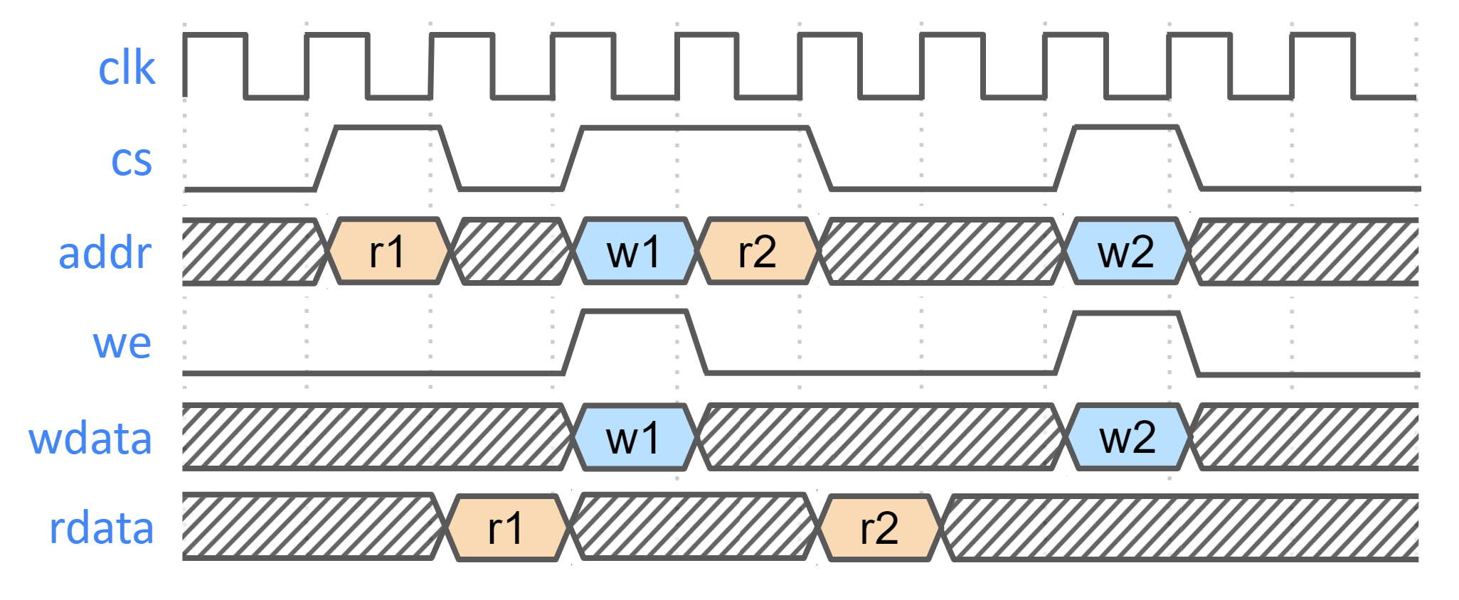
SRAM timing behavior
- [Writes] SRAM input wren signal is asserted simultaneously with input data and address. Input data is stored at the input address 1 clock cycle later.
- [Reads] SRAM input clock enable signal is asserted simultaneously with input address. Output data is available 1 clock cycle later from a flip-flop register stage.
The following figure shows the SRAM interface timing.
Figure: SRAM interface timing
SRAM parameterization
Parameterization for ICCM/DCCM/I-Cache memories is derived from the configuration of the VeeR RISC-V core that has been selected for Caliptra Subsystem integration. Parameters defined in the VeeR core determine signal dimensions at the Subsystem top-level interface and drive requirements for SRAM layout. For details about interface parameterization, see the Interfaces & Signals section.
Example SRAM machine check reliability integration
This section describes an example implementation of integrator machine check reliability.
This example is applicable to scenarios where an integrator may need control of or visibility into SRAM errors for purposes of reliability or functional safety. In such cases, integrators may introduce additional layers of error injection, detection, and correction logic surrounding SRAMs. The addition of such logic is transparent to the correct function of Caliptra Subsystem, and removes integrator dependency on Caliptra Subsystem components for error logging or injection.
Note that the example assumes that data and ECC codes are in non-deterministic bit-position in the exposed SRAM interface bus. Accordingly, redundant correction coding is shown in the integrator level logic (i.e., integrator_ecc(caliptra_data, caliptra_ecc)). If the Caliptra Subsystem data and ECC are deterministically separable at the Caliptra Subsystem interface, the integrator would have discretion to store the ECC codes directly and calculate integrator ECC codes for the data alone.
Figure: Example machine check reliability implementation
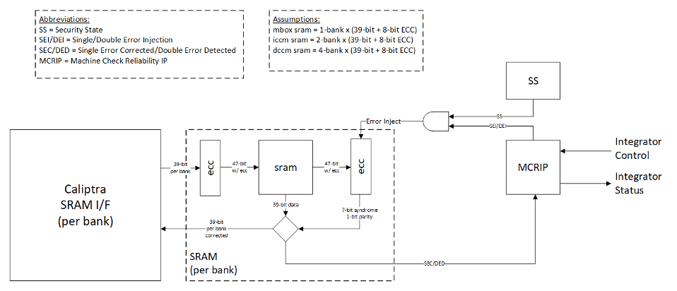
Error detection and logging
- Caliptra Subsystem IP shall interface to ECC protected memories.
- Caliptra Subsystem IP calculates and applies its own ECC code, which produces a total of 39-bit data written to external or INTEGRATOR instantiated SRAMs.
- Each 39-bit bank memory internally calculates 8-bit ECC on a write and stores 47 bits of data with ECC into SRAM.
- On read access syndrome is calculated based on 39-bit data.
- If parity error is detected and syndrome is valid, then the error is deemed single-bit and correctable.
- If no parity error is detected but syndrome == 0 or the syndrome is invalid, the error is deemed uncorrectable.
- On both single and double errors, the read data is modified before being returned to Caliptra Subsystem.
- Since single-bit errors shall be corrected through INTEGRATOR instantiated logic, Caliptra Subsystem never sees single-bit errors from SRAM.
- Double-bit or uncorrectable errors would cause unpredictable data to be returned to Caliptra Subsystem. Since this condition shall be detected and reported to MCRIP, there is no concern or expectation that Caliptra Subsystem will operate correctly after a double error.
- On detection, single errors are reported as transparent to MCRIP, double errors are reported as fatal.
- Along with error severity, MCRIP logs physical location of the error.
- After MCRIP logs an error, it has a choice to send out in-band notification to an external agent.
- MCRIP logs can be queried by SoC software.
Error injection
- MCRIP supports two error injection modes: intrusive and non-intrusive.
- Intrusive error injection:
- Can force a single or double error to be injected, which would result in incorrect data to be returned on read access.
- The intrusive error injection mode is disabled in Production fused parts via Security State signal.
- Non-intrusive error injection:
- Allows external software to write into MCRIP error log registers.
- The non-intrusive error injection does not interfere with the operation of memories.
- The non-intrusive error injection is functional in Production fused parts.
Caliptra Subsystem error handling flow
- Any implementation of error and recovery flows must adhere to the error handling requirements specified in Caliptra.md
- See MCI error handling for more details on MCI error infrastructure and error handling in Caliptra Subsystem.
- SoC level reporting and handling of fatal & non-fatal errors is product-specific architecture, outside the scope of Caliptra Subsystem definition. For example, a CPU and a PCIe device may handle fatal and non-fatal errors differently.
Programming interface
There are two primary programming avenues to interface with the Caliptra Subsystem:
-
MCU Firmware
- Description: This method involves programming the Microcontroller Unit (MCU) to execute firmware.
- Details: For more information on how to program the MCU and execute firmware via the MCU, please refer to the MCU Programming Interface documentation.
-
Caliptra Firmware
- Description: This method involves programming the Caliptra Core to execute firmware.
- Details: For more information on how to program and execute Caliptra Core firmware, please refer to the Caliptra Core References and Related Specifications.
Sequences
Reset Sequence:
- De-assert
cptra_ss_rst_b_iafter the primary clock (clk_i) stabilizes.
How to test
Reference tests are available at caliptra-ss\src\integration\test_suites
| Test Suite Name | Description |
|---|---|
MCU_HELLO_WORLD | Runs a basic "Hello World" program on the MCU to verify basic operation. |
MCU_CPTRA_BRINGUP | Tests the bring-up sequence of the MCU in the Caliptra Subsystem. |
MCU_DCCM_ACCESS | Validates access to the Data Closely Coupled Memory (DCCM) by the MCU. |
MCU_FUSE_CTRL_BRINGUP | Tests the bring-up sequence of the Fuse Controller by the MCU. |
MCU_LMEM_EXE | Tests execution by MCU from the MCU SRAM, contained inside the MCI component. LMEM refers to Local Memory, a generic alias for MCU SRAM. |
MCU_MCTP_SMOKE_TEST | Test verifies the I3C main target operation |
MCU_TEST_ROM_I3C_STREAMING_BOOT | Test verifies the I3C recovery target operation by using caliptra test ROM |
FUSE_PROV_WITH_LC_CTRL | Tests fuse provisioning in conjunction with the Lifecycle Controller. |
CALIPTRA_SS_LC_CTRL_BRINGUP | Tests the bring-up sequence of the Lifecycle Controller. |
CALIPTRA_SS_LC_CTRL_ST_TRANS | Validates state transitions of the Lifecycle Controller. |
Caliptra Core
Follow the link for Caliptra Core Integration Specification
MCU (Manufacturer Control Unit)
Overview
MCU is encapsulates VeeR EL2 core that includes an iCache, a dedicated DCCM, and AXI interfaces with separate AXI USER IDs to ROM and MCI. For more details refer to RISCV VeeR-EL2 Overview
Parameters & Defines
The VeeR EL2 core instance used for MCU has been configured with these options:
- DCCM size: 16KiB (see MCU DCCM SRAM Sizing)
- I-Cache depth: 16KiB
- ICCM: Disabled
- External Interrupt Vectors: 255
The following files from the Caliptra Subsystem repository contain the MCU configuration. Review these files for comprehensive list of MCU capabilities.
src/riscv_core/veer_el2/rtl/defines/css_mcu0_common_defines.vh
src/riscv_core/veer_el2/rtl/defines/css_mcu0_el2_param.vh
src/riscv_core/veer_el2/rtl/defines/css_mcu0_el2_pdef.vh
src/riscv_core/veer_el2/rtl/defines/defines.h
MCU Integration Requirements
-
Ensure Proper Memory Mapping
- The memory layout must match the physical memory configuration of the SoC.
- If modifications are required, update the base addresses and section placements accordingly.
- The address regions assigned to PIC and DCCM must not include any other AXI subordinates on the interconnect.
-
Enabling Programming interface.
- Please refer to section MCU Programming Interface for details on reference linker file for the MCU bringup.
MCU Core Configuration Customization
The MCU VeeR-EL2 core can be customized by integrators to optimize for specific SoC requirements.
Common Use Cases:
- Memory Architecture: Modify ICCM/DCCM addresses and sizes for SoC memory integration
- Power/Area Optimization: Remove or modify features (caching, number of interrupts)
- Performance Tuning: Adjust cache sizes and pipeline configurations for application workloads
Configuration Instructions:
Refer to the MCU Veer-EL2 Core Configuration section in the project README for complete step-by-step procedures.
Validation:
Execute the full regression test suite documented in How to test after any configuration changes to ensure system compatibility.
MCU DCCM SRAM Sizing
MCU's DCCM SRAM should be sized large enough to accommodate FW's stack and heap. If it is undersized, the MCU would have to rely on the MCU SRAM (accessed via AXI) for the stack/heap which has much lower performance.
MCU SRAM MRAC Considerations
The MCU's Memory Region Access Control (MRAC) regions are hard coded to 256MB boundaries. Each 256MB region is configured with uniform attributes - everything within a region is labeled as either "side effect" or "cacheable". This affects how MCU SRAM and MCU MBOX SRAM (both located within MCI) should be integrated into the SoC memory map, as different components within MCI may require different access attributes.
Split Memory Mapping
Integrators have two main approaches for handling MCI memory mapping:
Option 1: Contiguous MCI Address Region - If integrators don't care about the MRAC limitations described in the following sections, they can use a standard contiguous MCI address map where all MCI components (including MCU SRAM and MCU MBOX SRAM) reside within a single 256MB region.
Option 2: Split Memory Mapping - Integrators can optionally split MCU SRAM and MCU MBOX SRAMs into their own dedicated 256MB regions, separate from other MCI components. This allows firmware to enable caching or disable side effects for these specific SRAMs.
Side Effect Considerations
When MCU SRAM and MCU MBOX SRAM remain within the main MCI address space (not split off), integrators should consider the following access limitations:
DWORD Access Requirement: MCI peripherals (MCI CSRs, MCU trace buffer CSRs, etc) require "side effect" attribute enabled. When "side effect" is enabled dword-aligned accesses are required. Unaligned accesses, like accessing a uint8_t, are not permitted and will result in a read fault error in the MCU.
If you want to avoid these DWORD alignment limitations and allow more flexible access patterns, you can choose to implement the Split Memory Mapping (Option 2) in your AXI interconnect for MCU SRAM and/or MCU MBOX SRAM. This allows the SRAMs to be placed in regions without the side effect attribute.
iCache Considerations
When MCU SRAM remains within the main MCI address space (not split off), integrators should consider the following caching limitations:
iCache Enablement Requirement: To enable MCU iCache, everything within the 256MB boundary containing MCU SRAM must be cacheable. Since not all regions of MCI are cacheable, MCU iCache cannot be enabled when using a contiguous MCI address map.
If you want to enable MCU iCache functionality, you must implement the Split Memory Mapping (Option 2) in your AXI interconnect. This allows MCU SRAM to be placed in a dedicated cacheable region separate from other MCI components.
MCU Programming interface
MCU Linker Script Integration
This linker script defines the memory layout for the MCU firmware. It specifies the placement of various sections, ensuring proper memory mapping and execution flow.
Example Linker File can be found at : integration/test_suite/libs/riscv_hw_if/link.ld
By following this linker script configuration, the validation firmware can be correctly mapped and executed within the Caliptra Subsystem. Memory mapping for the validation firmware follows these principles:
- Instructions are stored in ROM for initial boot (.text)
- Read-only data is stored in ROM
- Stack and data sections are allocated to DCCM
- MCU SRAM is used for any combination of instructions and data to demonstrate program execution, data storage and persistence, streaming boot operations, and region protections that are enforced by MCI. Test firmware and corresponding linker scripts may be found in the repository test suites directory.
MCU External Interrupt Connections
| External interrupt vector | Description |
|---|---|
| 1 | MCI interrupts see MCI interrupt spec and MCI interrupt registers |
| 2 | I3C Interrupts |
| 255:3 | Exposed to SOC via cptra_ss_mcu_ext_int |
Fuse Controller
Overview
The Fuse Controller is a core component in the secure infrastructure of the system, responsible for managing the fuses and ensuring the integrity, consistency, and secure storage of sensitive data. It provides essential interfaces for direct fuse programming. The Fuse Controller interacts closely with the Lifecycle Controller (LC), FUSE macros, MCI, and Caliptra Core.
For an in-depth understanding of the Fuse Controller's functionality, including its programming flow, refer to Caliptra Subsystem Hardware Specification Document.
Parameters & Defines
| Parameter | Default | Description |
|---|---|---|
AlertAsyncOn | 5 | Enables asynchronous transitions on alerts. |
MemInitFile | "" | Hex file to initialize the OTP macro, including ECC. |
Interface
| Facing | Type | Width | Name | External Name in SoC Level | Description |
|---|---|---|---|---|---|
| External | Input | 1 | clk_i | cptra_ss_clk_i | Fuse Controller clock input. |
| External | Input | 1 | rst_ni | cptra_ss_rst_b_i | Reset signal input, active low. |
| Internal | Input | 1 | FIPS_ZEROIZATION_CMD_i | Fuse Zeroization signal controlled by MCI | |
| External | interface | 1 | core_axi_wr_req | cptra_ss_otp_core_axi_wr_req_i | AXI write request. |
| External | interface | 1 | core_axi_wr_rsp | cptra_ss_otp_core_axi_wr_rsp_o | AXI write response. |
| External | interface | 1 | core_axi_rd_req | cptra_ss_otp_core_axi_rd_req_i | AXI read request. |
| External | interface | 1 | core_axi_rd_rsp | cptra_ss_otp_core_axi_rd_rsp_o | AXI read response. |
| Internal | Output | 1 | intr_otp_operation_done_o | Indicates that the OTP operation has completed. | |
| Internal | Output | 1 | intr_otp_error_o | OTP error interrupt output (to be connected to MCI). | |
| Internal | Output | 5 | alerts | Alert signals for critical errors. | |
| Internal | Input | 1 | pwr_otp_i | OTP initialization request from the power manager. | |
| Internal | Output | Struct | pwr_otp_o | OTP response to the power manager. | |
| Internal | Input | Struct | lc_otp_vendor_test_i | Vendor test request input from LC Controller. | |
| Internal | Output | Struct | lc_otp_vendor_test_o | Vendor test response to LC Controller. | |
| Internal | Input | Struct | lc_otp_program_i | Lifecycle OTP programming request from LC Controller. | |
| Internal | Output | Struct | lc_otp_program_o | Lifecycle OTP programming response to LC Controller. | |
| Internal | Input | 1 | lc_dft_en_i | DFT enable input from LC Controller. | |
| Internal | Input | 1 | lc_escalate_en_i | Escalation enable input from LC Controller. | |
| Internal | Input | 1 | lc_check_byp_en_i | Clock bypass check enable input from LC Controller. | |
| Internal | Output | Struct | otp_lc_data_o | Lifecycle broadcasted data output to LC Controller. | |
| Internal | Output | Struct | otp_broadcast_o | FUSE broadcast output to Caliptra Core. This port broadcasts UDS-seed and Field-entropy-seed. |
Fuse Macro Memory Map and Fuse Controller CSR Address Map
The Caliptra Subsystem fuse controller supports a flexible and extensible memory map for storing one-time programmable (OTP) data. This structure is documented in the following files: See Fuse Controller Register Map for registers. See Fuse Macor Memory Map for fuse partition map.
The current fuse memory map consists of three main architectural segments: Caliptra-Core (prefix: CALIPTRA_CORE), Caliptra-Subsystem (prefix: CALIPTRA_SS), SoC/Vendor-Specific.
This structure enables separation of responsibilities and flexibility in SoC integration. While the Caliptra-Core fuse items are mandatory and must adhere to the Caliptra Fuse Map Specification, Caliptra-Subsystem fuses are required only when the subsystem is instantiated with Caliptra Subsystem. These Caliptra Subsystem fuses can also be configured based on SoC requirements. The SoC/Vendor-specific items can be customized based on integrator needs and product requirements. Therefore, the fields under SoC-specific categories can be resized or eliminated if unused.
SOC_SPECIFIC_IDEVID_CERTIFICATE Usage
This field defaults to 4 bytes but can be extended to accommodate storage of a full IDevID hybrid certificate (e.g., ML-DSA + ECC) if desired. Integrators must adjust its size in the YAML config used by the generation script.
FC Integration Requirements
Connectivity, Clock & Reset, Constraints & Violations
-
Connectivity:
- The Fuse Controller must interface seamlessly with the Fuse Macros, ensuring proper ECC support during programming and read operations.
- All AXI interfaces (
core_axi_wr_req,core_axi_rd_req) must follow the protocol specifications. - Inputs like
lc_otp_program_iandpwr_otp_ishould connect properly to the Lifecycle Controller (LC) and MCI respectively. - Alerts must propagate correctly to the system's alert manager for error handling.
-
Constraints & Violations:
- Any access to fuses must be gated by the
FUSE_CTRL_DIRECT_ACCESS_REGWENbit to prevent unauthorized writes. - There are some fuses that can be programmed only by Caliptra Core. Therefore, each AXI write should follow the access permission rule defined by
access_control_tableinsrc/fuse_ctrl/rtl/otp_ctrl_pkg.sv. - Timeout conditions during consistency checks (
FUSE_CTRL_CHECK_TIMEOUT) should trigger appropriate alerts. - Errors like invalid data, ECC failures, or access violations should raise alerts via the
alertssignal.
- Any access to fuses must be gated by the
-
Scan Path Exclusions:
- Ensure that secret fuse fields (UDS and Field-Entropy) and their corresponding flip-flops are not a parth of the scan path. Specifically, in this version, there are five OTP partitions that contain secrets that must not be leaked:
SECRET_MANUF_PARTITION: that contains the UDS seed, andSECRET_PROD_PARTITION_{0,1,2,3}: that each contain field entropy. These fuse partitions are "Buffered" partitions, meaning they are sensed at power-on and buffered in flip-flops until the next reset. During SoC integration it is vital to exclude the buffering flops that hold sensitive secret data from the scan chain to avoid leaks. These buffering flops may be excluded from the scan chain by excluding the following hierarchies:**::u_otp_ctrl::u_part_buf::u_otp_ctrl_ecc_reg::gen_partitions[X]::gen_buffered::u_part_buf::u_otp_ctrl_ecc_reg::**, for all values ofXin 1–5, since indices 1–5 map to the sensitive partitions mentioned above (defined in thePartInfolocalparam inotp_ctrl_part_pkg.sv, autogenerated from the OTP memory map HJSON). Additionally, these secrets are broadcasted with this input port:otp_broadcast_o. Therefore, this port, its propagated signals, and its driver signals must also not be scannable.
- Ensure that secret fuse fields (UDS and Field-Entropy) and their corresponding flip-flops are not a parth of the scan path. Specifically, in this version, there are five OTP partitions that contain secrets that must not be leaked:
- Since Fuse Controller scrambles secret partition with PRESENT chipher, this chiper keys, autogenerated from the OTP memory map HJSON, must be excluded from the scan path. Although these values are parameters defined in
otp_ctrl_part_pkg.sv, the registers driven by these parameters must be excluded from the scan path. - Note, the LC token partitions are not considered secret as only the cSHAKE128 hashes of each token are stored, not the raw tokens themselves.
Direct Access Interface
Fuse macros has to be programmed via the Direct Access Interface, which is comprised of the following CSRs:
| CSR Name | Description |
|---|---|
DIRECT_ACCESS_WDATA_0 | Low 32bit word to be written. |
DIRECT_ACCESS_WDATA_1 | High 32bit word to be written. |
DIRECT_ACCESS_RDATA_0 | Low 32bit word that has been read. |
DIRECT_ACCESS_RDATA_1 | High 32bit word that has been read. |
DIRECT_ACCESS_ADDRESS | byte address for the access. |
DIRECT_ACCESS_CMD | Command register to trigger a read or a write access. |
DIRECT_ACCESS_REGWEN | Write protection register for DAI. |
Initialization
The OTP controller initializes automatically upon power-up and is fully operational by the time the processor boots. The only initialization steps that SW should perform are:
- Check that the OTP controller has successfully initialized by reading
STATUS. I.e., make sure that none of the ERROR bits are set, and that the DAI is idle (STATUS.DAI_IDLE).- Choose whether the periodic background checks shall be subject to a timeout by programming a nonzero timeout cycle count to
CHECK_TIMEOUT. In this case, theCHECK_TIMEOUTregister must be set before theINTEGRITY_CHECK_PERIODandCONSISTENCY_CHECK_PERIODregisters (see next point). - Enable periodic background checks by programming nonzero mask values to
INTEGRITY_CHECK_PERIODandCONSISTENCY_CHECK_PERIOD. - It is recommended to lock down the background check registers via
CHECK_REGWEN, once the background checks have been set up
- Choose whether the periodic background checks shall be subject to a timeout by programming a nonzero timeout cycle count to
If needed, one-off integrity and consistency checks can be triggered via CHECK_TRIGGER.
If this functionality is not needed, it is recommended to lock down the trigger register via CHECK_TRIGGER_REGWEN.
Programming interface
The Fuse Controller (FC) programming interface is designed to manage lifecycle states, handle fuses with ECC support, and ensure secure interactions with the fuse macros. A key component in this architecture is the Fuse Controller Filter RTL. This module intercepts and verifies the fuse programming sequence by checking that all parts of the transaction originate from the same authorized source. In doing so, the filter guarantees that fuse provisioning is performed in an atomic manner.
Atomic fuse provisioning means that only one entity can initiate the programming sequence at a time. The entire sequence—data write, address write, and command write—must complete successfully. If any phase fails or if an inconsistency is detected (for example, if the AXI user ID changes between phases), the operation is aborted, and a cold reset is required before any new programming attempt can be made.
The access control table, which defines allowed fuse address ranges along with the corresponding authorized AXI user IDs. See access_control_table in src/fuse_ctrl/rtl/otp_ctrl_pkg.sv.
Below are the key operations supported by the programming interface:
-
Direct Access Interface (DAI):
- Registers:
FUSE_CTRL_DIRECT_ACCESS_CMD: Specifies the operation (FUSE_CTRL_CMD_DAI_WRITEfor write,FUSE_CTRL_CMD_DAI_READfor read).FUSE_CTRL_DIRECT_ACCESS_ADDRESS: Specifies the fuse memory address to access.FUSE_CTRL_DIRECT_ACCESS_WDATA_0: Write data (32-bit granularity).FUSE_CTRL_DIRECT_ACCESS_WDATA_1: Write data for 64-bit operations.FUSE_CTRL_DIRECT_ACCESS_RDATA_0: Read data (32-bit granularity).FUSE_CTRL_DIRECT_ACCESS_RDATA_1: Read data for 64-bit operations.
- Procedure:
- Write the address to
FUSE_CTRL_DIRECT_ACCESS_ADDRESS. - For write operations:
- Populate
FUSE_CTRL_DIRECT_ACCESS_WDATA_0(andFUSE_CTRL_DIRECT_ACCESS_WDATA_1for 64-bit operations).
- Populate
- Set the command in
FUSE_CTRL_DIRECT_ACCESS_CMD. - Wait for the operation to complete by polling the
DAI_IDLEbit inFUSE_CTRL_STATUS.
- Write the address to
- ECC Support:
- ECC is automatically applied during programming to ensure data integrity.
- Registers:
-
Digest Calculation:
- Used to lock a partition after programming is complete.
- Registers:
FUSE_CTRL_DIRECT_ACCESS_CMD: Use command0x4for digest calculation.FUSE_CTRL_DIRECT_ACCESS_ADDRESS: Partition base address.
- Procedure:
- Write the partition base address to
FUSE_CTRL_DIRECT_ACCESS_ADDRESS. - Trigger the digest calculation command (
0x4) inFUSE_CTRL_DIRECT_ACCESS_CMD. - Poll the
DAI_IDLEbit inFUSE_CTRL_STATUSto confirm the operation is complete.
- Write the partition base address to
Readout Sequence
A typical readout sequence looks as follows:
- Check whether the DAI is idle by reading the
STATUSregister. - Write the byte address for the access to
DIRECT_ACCESS_ADDRESS. Note that the address is aligned with the granule, meaning that either 2 or 3 LSBs of the address are ignored, depending on whether the access granule is 32 or 64bit. - Trigger a read command by writing 0x1 to
DIRECT_ACCESS_CMD. - Poll the
STATUSuntil the DAI state goes back to idle. Alternatively, theotp_operation_doneinterrupt can be enabled up to notify the processor once an access has completed. - If the status register flags a DAI error, additional handling is required.
- If the region accessed has a 32bit access granule, the 32bit chunk of read data can be read from
DIRECT_ACCESS_RDATA_0. If the region accessed has a 64bit access granule, the 64bit chunk of read data can be read from theDIRECT_ACCESS_RDATA_0andDIRECT_ACCESS_RDATA_1registers. - Go back to the first step and repeat until all data has been read.
The hardware will set DIRECT_ACCESS_REGWEN to 0x0 while an operation is pending in order to temporarily lock write access to the CSRs registers.
Sequences: Reset, Boot
-
Reset Sequence:
- De-assert
rst_niafter the primary clock (clk_i) stabilizes. - Verify reset state by reading
FUSE_CTRL_STATUS. All errors in the status register should be 0. - Ensure Fuse Macros are in their default state after reset.
- De-assert
-
Boot Sequence:
- Initialize Fuse Macros by programming essential fuses using the programming interface.
- Perform a full integrity check by triggering
FUSE_CTRL_CHECK_TRIGGERand ensure the system is error-free before proceeding. - Validate readiness by checking the
FUSE_CTRL_STATUSregister.
How to test : Smoke & more
The smoke test focuses on ensuring basic functionality and connectivity of the FC & LCC. TODO More details will be provided once FC is ready to test.
Generating the Fuse Partitions
The configurable parts of the fuse_ctrl, specifically the fuse map and register interface,
are bootstrapped through a separate script ./tools/scripts/fuse_ctrl_script/gen_fuse_ctrl_partitions.py.
For a detailed breakdown of the design rationale behind the script as well as execution instructions,
refer to Fuse Map Generation Script.
Fuse Controller Macro
The following integration section is based on the Generalized Open-source Interface with modifications to match the Caliptra implementation.
Overview
The Fuse Controller Macro implements a generalized open-source interface for functional operation (described below). Any OTP redundancy mechanism like per-word ECC is assumed to be handled inside the wrapper, which means that the word width exposed as part of the generalized interface is the effective word width.
Paramteres & Defines
| Parameter | Default | Description |
|---|---|---|
Width | 16 | Width of native OTP words. |
AddrWidth | Derived | Width of the address signal, derived from Depth. |
Depth | `2**OtpAddrWidth | Depth of OTP macro. |
CmdWidth | 7 | Width of the OTP command. Sparsely encoded. |
ErrWidth | 3 | Width of error code output signal. |
SizeWidth | 2 | Width of the size input field. Allows to transfer up to 4 native OTP words at once. |
PwrSeqWidth | "" | Hex file to initialize the OTP macro, including ECC. |
IfWidth | 2**OtpSizeWidth*OtpWidth | Width of the wrapper data interface. |
FC Macro Integration Requirements
The generalized open-source interface is a simple command interface with a ready / valid handshake that makes it possible to introduce back pressure if the OTP macro is not able to accept a command due to an ongoing operation.
In order to facilitate the scrambling and digest operations, the data width has been sized such that data blocks up to the PRESENT block size (64bit) can be transferred across the generalized interface. The actual size of a transfer is determined via the size_i field. Transfer sizes are specified in multiples of the native OTP block size, as listed below.
Value of size_i | #Native OTP Words | Bit Slice |
|---|---|---|
| 2'b00 | 1 | {word0} = data[15:0] |
| 2'b01 | 2 | {word1, word0} = data[31:0] |
| 2'b10 | 3 | {word2, word1, word0} = data[47:0] |
| 2'b11 | 4 | {word3, word2, word1, word0} = data[63:0] |
Responses are returned in-order via an unidirectional response interface (i.e., without back pressure capability). Downstream logic must be able to sink the response in any case. The response optionally carries read data, depending on whether the operation that took place was a read or not. Also, an error signal returns a non-zero error code in case an error occurred while carrying out the OTP command.
The signals pertaining to the generalized open-source interface are listed below.
The signals are exposed as cptra_ss_fuse_macro_outputs_i and
cptra_ss_fuse_macro_inputs_o at the top level.
| Signal | Type | Width | Description |
|---|---|---|---|
cptra_ss_fuse_macro_inputs_o.valid_i | Input | 1 | Valid signal for the command handshake. |
cptra_ss_fuse_macro_inputs_o.size_i | Input | [SizeWidth-1:0] | Number of native OTP words to transfer, minus one: 2'b00 = 1 native word ... 2'b11 = 4 native words. |
cptra_ss_fuse_macro_inputs_o.cmd_i | Input | [CmdWidth-1:0] | OTP command: 7'b1000101 = read, 7'b0110111 = write, 7'b1111001 = read raw, 7'b1100010 = write raw, 7'b0101100 = initialize |
cptra_ss_fuse_macro_inputs_o.addr_i | Input | [$clog2(Depth)-1:0] | OTP word address. |
cptra_ss_fuse_macro_inputs_o.wdata_i | Input | [IfWidth-1:0] | Write data for write commands. |
cptra_ss_fuse_macro_outputs_i.fatal_alert_o | Output | 1 | Fatal alert output from the FC macro. This is connected to a separate alert channel in the instantiating IP. The instantiating IP latches the alert indication and continuously outputs alert events until reset. |
cptra_ss_fuse_macro_outputs_i.ecov_alert_o | Output | 1 | Recoverable alert output from the FC macro. This is connected to a separate alert channel in the instantiating IP. Should only be pulsed high for each alert occurrence. The instantiating IP then sends out a single alert event for each pulse. |
cptra_ss_fuse_macro_outputs_i.ready_o | Output | 1 | Ready signal for the command handshake. |
cptra_ss_fuse_macro_outputs_i.valid_o | Output | 1 | Valid signal for command response. |
cptra_ss_fuse_macro_outputs_i.rdata_o | Output | [IfWidth-1:0] | Read data from read commands. |
cptra_ss_fuse_macro_outputs_i.err_o | Output | [ErrWidth-1:0] | Error code. |
The write raw and read raw command instructs the Fuse Controller Macro
wrapper to store / read the data in raw format without generating nor checking
integrity information. That means that the wrapper must return the raw,
uncorrected data and no integrity errors.
The Fuse Controller Macro wrapper implements the error codes (0x0 - 0x4).
| Error Code | Enum Name | Recoverable | DAI | LCI | Unbuf | Buf | Description |
|---|---|---|---|---|---|---|---|
| 0x0 | NoError | - | x | x | x | x | No error has occurred. |
| 0x1 | MacroError | no | x | x | x | x | Returned if the OTP macro command did not complete successfully due to a macro malfunction. |
| 0x2 | MacroEccCorrError | yes | x | - | x | x | A correctable ECC error has occurred during a read operation in the OTP macro. |
| 0x3 | MacroEccUncorrError | no | x | - | x* | x | An uncorrectable ECC error has occurred during a read operation in the OTP macro. Note (*): This error is collapsed into MacroEccCorrError if the partition is a vendor test partition. It then becomes a recoverable error. |
| 0x4 | MacroWriteBlankError | yes / no* | x | x | - | - | This error is returned if a write operation attempted to clear an already programmed bit location. Note (*): This error is recoverable if encountered in the DAI, but unrecoverable if encountered in the LCI. |
The timing diagram below illustrates the timing of a command. Note that both read and write commands return a response, and each command is independent of the previously issued commands. The latency from accepting a command to returning a response depends on the underlying OTP IP and is typically larger than 10 cycles. The returned values depend on the command type and whether an error occurred or not.
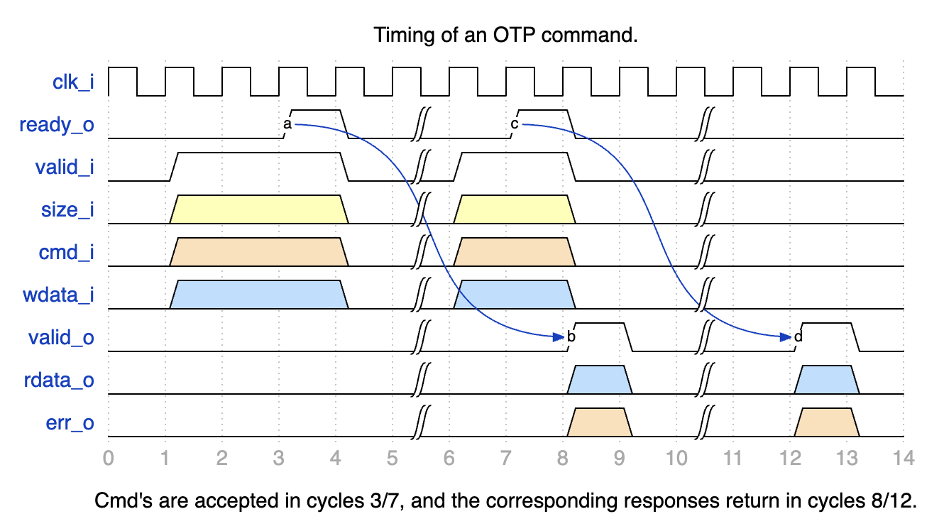
Note that the default configuration of the Fuse Controller allows up to two outstanding OTP commands, meaning that it is permissible to acknowledge an incoming command and start working on it while the results of the last command are still in the process of being output (e.g., due to an output register stage).
The Fuse Controller Macro uses the following signals to interface with the Fuse Controller.
Generic Strap Port Usage for FC Register Locations
To support flexible integration across varying fuse partition generations, Caliptra ROM uses two generic strap ports to locate fuse controller registers.
Why These Straps Are Needed
Each fuse partition generation introduces new error bits into the status register. This causes the idle bit to shift leftward, changing its position within the SOC_OTP_CTRL_STATUS register. Similarly, the CMD register may shift downward in memory if new fuse partition definitions introduce additional registers like ADDR, WDATA0, RDATA0, etc.
Because of these dynamic shifts:
- The idle bit location cannot be hardcoded.
- The CMD register address must be explicitly provided, even though the other fuse controller registers are laid out consecutively.
Strap Definitions
-
cptra_ss_strap_generic_0_iA 32-bit input strap that encodes:- Upper 16 bits: Bit index of the idle status bit (
IDLE_BIT_STATUS) withinSOC_OTP_CTRL_STATUS. - Lower 16 bits: Offset address of
SOC_OTP_CTRL_STATUSwithin theSOC_IFC_REGspace, relative toSOC_OTP_CTRL_BASE_ADDR.
This allows the ROM to accurately monitor the fuse controller's idle state regardless of partition-induced shifts.
- Upper 16 bits: Bit index of the idle status bit (
-
cptra_ss_strap_generic_1_iA 32-bit input strap that provides the address of the CMD register. Since the fuse controller registers are laid out consecutively, specifying the CMD register is sufficient for the ROM to infer the locations of adjacent registers likeADDR,WDATA0, andRDATA0.
FC Macro Test Interface
The Fuse Controller Macro requires a test interface to be able to access the underlying OTP debug access interface and power manager controller. During early manufacturing, the test interface can be used to run BIST and repair flows before performing a non-volatile raw unlock operation.
For security reasons, it must be ensured that it is not possible to read / program arbitrary OTP memory locations through the test interface. Only specific, pre-defined test locations shall be readable and programmable. Access to debug access interface must also be disabled once the device is in mission mode (i.e. PROD life cycle state).
Life Cycle Controller
Overview
The LC Controller (Lifecycle Controller) is a critical component of the Caliptra Subsystem, responsible for securely managing the lifecycle states of the chip. The LC Controller interacts with other subsystems such as the Fuse Controller, MCI, AXI interconnect, and JTAG TAP to enforce secure transitions, validate tokens, and generate error conditions. Additionally, it implements escalation mechanisms to respond to security breaches, enabling the chip to enter secure states like SCRAP.
For a detailed description of the Lifecycle Controller's architecture, design, and operational flow, refer to Caliptra Subsystem Hardware Specification Document.
Parameters & Defines
| Parameter | Default (Max) | Description |
|---|---|---|
AlertAsyncOn | 2'b11 | |
IdcodeValue | 32'h00000001 | Idcode for the LC JTAG TAP. |
RndCnstLcKeymgrDivInvalid | (see RTL) | Diversification value used for all invalid life cycle states. |
RndCnstLcKeymgrDivTestUnlocked | (see RTL) | Diversification value used for the TEST_UNLOCKED* life cycle states. |
RndCnstLcKeymgrDivDev | (see RTL) | Diversification value used for the DEV life cycle state. |
RndCnstLcKeymgrDivProduction | (see RTL) | Diversification value used for the PROD/PROD_END life cycle states. |
RndCnstLcKeymgrDivRma | (see RTL) | Diversification value used for the RMA life cycle state. |
SecVolatileRawUnlockEn | 1'b1 | Enables Volatile TEST_UNLOCKED0 state transition infra |
Interface
| Facing | Type | width | Name | External Name in SoC Level | Description |
|---|---|---|---|---|---|
| External | input | 1 | clk_i | cptra_ss_clk_i | clock |
| External | input | 1 | rst_ni | cptra_ss_rst_b_i | LC controller reset input, active low |
| External | input | 1 | raw_unlock_token_hashed_i | cptra_ss_raw_unlock_token_hashed_i | Hashed token for RAW unlock |
| External | input | 1 | Allow_RMA_or_SCRAP_on_PPD | cptra_ss_lc_Allow_RMA_or_SCRAP_on_PPD_i | This is GPIO strap pin. This pin should be high until LC completes its state transition to RMA or SCRAP. |
| External | interface | 1 | axi_wr_req | cptra_ss_lc_axi_wr_req_i | LC controller AXI write request input |
| External | interface | 1 | axi_wr_rsp | cptra_ss_lc_axi_wr_rsp_o | LC controller AXI write response output |
| External | interface | 1 | axi_rd_req | cptra_ss_lc_axi_rd_req_i | LC controller AXI read request input |
| External | interface | 1 | axi_rd_rsp | cptra_ss_lc_axi_rd_rsp_o | LC controller AXI read response output |
| External | interface | 1 | jtag_i | cptra_ss_lc_ctrl_jtag_i | LC controller JTAG input ports |
| External | interface | 1 | jtag_o | cptra_ss_lc_ctrl_jtag_o | LC controller JTAG output ports |
| External | input | 1 | scan_rst_ni | cptra_ss_lc_ctrl_scan_rst_ni_i | LC controller scan reset input, active low |
| Internal | output | 3 | alerts | Alert outputs generated by LCC if there is an error due to one of following: register bus, lc state and fuse programming | |
| External | input | 1 | esc_scrap_state0 | cptra_ss_lc_esclate_scrap_state0_i | An escalation input that leads LC controller to enter into SCRAP mode |
| External | input | 1 | esc_scrap_state1 | cptra_ss_lc_esclate_scrap_state1_i | An escalation input that eads LC controller to enter into SCRAP mode |
| Internal | input | 1 | pwr_lc_i | A power initilization input coming from MCI | |
| Internal | struct | 1 | pwr_lc_o | Two outputs show: (i) LC controller can accept a request, (ii) LC is initialized. | |
| Internal | struct | 1 | lc_otp_vendor_test_o | Access to fuse controller for vendor test partitions | |
| Internal | struct | 1 | lc_otp_vendor_test_i | Access to fuse controller for vendor test partitions | |
| Internal | struct | 1 | lc_otp_program_o | Programming interface to fuse controller to update LCC state and couter | |
| Internal | struct | 1 | lc_otp_program_i | Programming interface from fuse controller to update LCC state and couter | |
| Internal | struct | 1 | otp_lc_data_i | Broadcasted values from the fuse controller | |
| Internal | output | 1 | lc_dft_en_o | DFT enable to MCI | |
| Internal | output | 1 | lc_hw_debug_en_o | CLTAP enable to MCI | |
| Internal | output | 1 | lc_escalate_en_o | Broadcast signal to promote esclation in SoC | |
| Internal | output | 1 | lc_check_byp_en_o | External clock status delivery signal to fuse controller | |
| External | output | 1 | lc_clk_byp_req_o | cptra_ss_lc_clk_byp_req_o | A request port to swtich from LCC clock to external clock |
| External | input | 1 | lc_clk_byp_ack_i | cptra_ss_lc_clk_byp_ack_i | Acknowledgment signal to indicate external clock request is accepted |
| Internal | input | 1 | otp_device_id_i | Unused port | |
| Internal | input | 1 | otp_manuf_state_i | Unused port | |
| Internal | output | 1 | hw_rev_o | Unused port | |
| Internal | input | 253 | cptra_ss_mcu_ext_int | Reflection of HW revision ID read from fuse controller |
Fuse Macro Memory Map / Fuse Controller CSR Address Map
See Life-cycle Controller Register Map.
LC Integration Requirements
Connectivity, Clock & Reset, Constraints & Violations
-
Connectivity:
- Ensure proper routing of all signals to avoid conflicts with other modules.
- Interfaces like
jtagandaximust adhere to the defined protocol specifications. - Escalation signals (
esc_scrap_state0andesc_scrap_state1) brings LC controller into temporal SCRAP mode (Escalation state) and therefore needs to be connected to a dedicated controller. Allow_RMA_or_SCRAP_on_PPDneeds to be tied 0 if it is not being used. Otherwise, it might break LC controller's internal FSM.- Avoid glitches on
Allow_RMA_or_SCRAP_on_PPDand escalation inputs (esc_scrap_state0,esc_scrap_state1) that could cause unintended transitions. - Verify that all output signals, including alerts, remain within the expected ranges under normal operation.
-
IMPORTANT SOC REQUIREMENT:
- Life cycle controller allows you to switch from internal to external clock on a request from SOC over JTAG or AXI (As explained in other sections, this is typically used for Fuse programming scenarios when a stable clock is not yet available within the SOC). When the request arrives, life cycle controller requests the SOC to do the clock switch. When such a request is made, SOC MUST respond with an acknowledgement within 2 clock cycles of the internal clock. If this condition is not met, OTP controller will assert "program error" and the SOC must go through a reset cycle and redo the above steps. This must be verified by the SOC as a part of Caliptra subsystem integration checks.
To protect from clock stretching attacks Caliptra mandates using a clock source that is constructed within the SOC (eg. PLL, Calibrated Ring Oscillator, etc). For such a clock source, a SOC may require fuses to be programmed. TP programming demands a reliable and deterministic clock signal to ensure correct fuse write operations; which SOC may not have during the early phases of manufacturing flow due to above constraints. In order to overcome this issue, this
external clockcan be used typically in the manufacturing phase of a SOC; and for such SOCs this external clock is supplied from a platform (e.g an ATE). Since the Caliptra subsystem includes only one clock input (cptra_ss_clk_i), the SoC integrator is responsible for ensuring that this input can be switched to a stable source.- The life-cycle controller exposes an
LC_STATEregister that carries the life-cycle controller state, which the SoC can read to determine the current life-cycle state. In addition, the Caliptra Subsystem top level provides thecaliptra_ss_life_cycle_steady_state_oandcaliptra_ss_otp_state_valid_osignals, which are broadcast from the fuse controller. Whenevercaliptra_ss_otp_state_valid_ois asserted,caliptra_ss_life_cycle_steady_state_oreflects the latest life-cycle state stored in the fuse macro. Because the fuse controller is initialized earlier than the life-cycle controller, these broadcast state signals are derived from the fuse controller. Note thatcaliptra_ss_otp_state_valid_ois driven low by the fuse controller if a fatal error occurs in the fuse controller or if an escalation signal is asserted by the life-cycle controller. In contrast,LC_STATEprovides the life-cycle controller’s own view of the state, independent of the fuse controller’s errors such as entering SCRAP state.
Volatile-unlock state transitions are not reflected by the fuse controller, and therefore
caliptra_ss_life_cycle_steady_state_oandcaliptra_ss_otp_state_valid_odo not capture state transitions granted exclusively by the life-cycle controller. To cover this case, the Caliptra Subsystem also broadcastscaliptra_ss_volatile_raw_unlock_success_o, which is asserted by the life-cycle controller to indicate that the volatile-unlock state has been granted. -
Scan Path Exclusions:
- Ensure that the RAW_UNLOCK token is excluded from the scan chain. This token is different from other LC transition tokens as it is stored in the plaintext in gates, not in hashed form.
To exclude it from scan, the following hierarchies must be excluded:
*::lc_ctrl_fsm::hashed_tokens_{higher, lower}[RawUnlockTokenIdx]and*::lc_ctrl_fsm::hashed_token_mux.
- Ensure that the RAW_UNLOCK token is excluded from the scan chain. This token is different from other LC transition tokens as it is stored in the plaintext in gates, not in hashed form.
To exclude it from scan, the following hierarchies must be excluded:
-
RAW Unlock Token:
- The
cptra_ss_raw_unlock_token_hashed_itop-level input defines the hashed value of the RAW unlock token. The hashed value is generated from the unhashed RAW unlock token, which the integrator must obtain from a cryptographically secure random number generator. Both the hashed and the unhashed token must be kept secret. To generate the hashed token (and optionally also the unhashed token),tools/scripts/lc_ctrl_script/gen_lc_ctrl_token.pycan be used. - The unhashed RAW unlock token is required in SW that performs a non-volatile RAW unlock.
- The hashed RAW unlock token is stored in HW (see first bullet point) and required in SW that performs a volatile RAW unlock.
- The
Programming Interface
The LC Controller's programming interface facilitates lifecycle state transitions, secure token authentication, and system initialization. Below are the key programming steps:
-
Initialization:
- Ensure the LC Controller is ready by polling the
LC_CTRL_STATUS_OFFSETregister for theREADY_MASKbit. - Verify initialization is complete using the
INIT_MASKbit in the same register. - Corresponding fuse partitions need to be provisioned in order to perform state transitions
- Ensure the LC Controller is ready by polling the
-
Lifecycle State Transitions:
- Claim the transition mutex by writing
0x96(MuBi8True) toLC_CTRL_CLAIM_TRANSITION_IF_OFFSETand polling until the value is correctly latched. - Set the desired next lifecycle state by writing to
LC_CTRL_TRANSITION_TARGET_OFFSET. - Write the 128-bit transition token (if required) into the
LC_CTRL_TRANSITION_TOKEN_*_OFFSETregisters. - Trigger the state transition by writing
0x1toLC_CTRL_TRANSITION_CMD_OFFSET. - Poll the
LC_CTRL_STATUS_OFFSETregister to monitor for successful state transition or detect errors such as token errors, OTP errors, or RMA strap violations. - Each TEST_UNLOCKED state has its own TOKEN (see See Fuse Memory Map).
- During a state transition, an asserted reset or zeorization command can cause permanent life-cycle state corruption.
- Claim the transition mutex by writing
-
Token Validation:
- For conditional state transitions, provide the transition token before the transition request.
- Toke Format is illustrated with a python implementation:
# value = 0x318372c87790628a05f493b472f04808
# data = value.to_bytes(16, byteorder='little')
# custom = 'LC_CTRL'.encode('UTF-8')
# shake = cSHAKE128.new(data=data, custom=custom)
# shake output is 0x4c9ca068a68474d526e7d8a0233d5aad

# To unlock a state having the shake condition above, the LCC needs
# to get the following input set:
TOKEN_write(LC_CTRL_TRANSITION_TOKEN_3_OFFSET, 0x318372c8)
TOKEN_write(LC_CTRL_TRANSITION_TOKEN_1_OFFSET, 0x7790628a)
TOKEN_write(LC_CTRL_TRANSITION_TOKEN_2_OFFSET, 0x05f493b4)
TOKEN_write(LC_CTRL_TRANSITION_TOKEN_0_OFFSET, 0x72f04808)
- RMA and SCRAP Strap Handling:
- Ensure the
Allow_RMA_or_SCRAP_on_PPDGPIO strap is asserted for RMA or SCRAP transitions. Transitions without this strap will fail with an appropriate status in theLC_CTRL_STATUS_OFFSETregister.
- Ensure the
Sequences: Reset, Boot
-
Reset Sequence:
- Bring the LC Controller out of reset by asserting and de-asserting
rst_niafter clock stabilization. - Perform a reset sequence after each state transition routine
- Bring the LC Controller out of reset by asserting and de-asserting
-
Boot Sequence:
- Enable MCI that intilaize the LC controller.
- Verify successful initialization by reading
LC_CTRL_STATUS_OFFSET.
-
Error Scenarios:
- Test scenarios where invalid tokens, Fuse errors, or missing RMA straps are injected to validate error handling and system recovery mechanisms.
How to Test: Smoke & More
Smoke Test
-
Basic Connectivity:
- Verify the LC Controller responds to read and write operations on key registers (e.g.,
LC_CTRL_STATUS_OFFSET,LC_CTRL_CLAIM_TRANSITION_IF_OFFSET).
- Verify the LC Controller responds to read and write operations on key registers (e.g.,
-
Basic Initialization:
- Check that the
READY_MASKandINIT_MASKbits inLC_CTRL_STATUS_OFFSETtransition to the expected values during initialization.
- Check that the
-
Lifecycle Transition:
- Perform a single state transition (e.g.,
RAWtoTEST_UNLOCKED0)
- Perform a single state transition (e.g.,
Functional Tests
-
Full Lifecycle Sequence:
- Run all lifecycle transition functions and validate each transition step via the status register and debug messages.
-
Error Injection:
- Test token errors by providing invalid tokens during a transition request.
- Simulate OTP errors by corrupting OTP data or configuration.
- Test RMA transitions with and without the
Allow_RMA_or_SCRAP_on_PPDGPIO strap. - Test SCRAP transitions with and without the
Allow_RMA_or_SCRAP_on_PPDGPIO strap.
-
Boundary Testing:
- Verify correct operation under boundary conditions, such as repeated transitions, simultaneous requests, or rapid reset sequences.
Advanced Tests
-
Stress Test:
- Perform rapid transitions through multiple lifecycle states to validate system robustness.
- Simulate power interruptions during critical operations.
-
Integration Tests:
- Verify interaction with other modules such as the fuse controller and MCI during state transitions.
MCI
Overview
Manufacturer Control Interface provides the following features for Caliptra SS:
-
Boot Sequencer for the SS
-
FC Init
-
LCC Init
-
MCU Reset
- Hitless Update Capability
-
-
Caliptra Reset
-
MCU SRAM
-
MCU Trace Buffer
-
MCU watchdog timer
-
Mailboxes
-
LCC State Translator for Caliptra Core
-
Error Aggregation
-
Register Bank for MCU/SOC
The Boot Sequence is what brings the subsystem up. It will do fuse controller and life cycle controller initialization. It then brings up MCU and Caliptra based on the breakpoint and no rom config input pins. Once MCI has done the subsystem bring up, it provides other functionality like the MCU SRAM, DAM for MCU, Error aggregation for the SS and more.
If there is an issue within MCI whether it be the Boot Sequencer or another component. The SOC can utilize the breakpoint and DMI capability to halt the Boot Sequencer before bring up the MCU and do targeted register accesses via the DMI port which is connected to the MCU.
MCI Block Diagram:
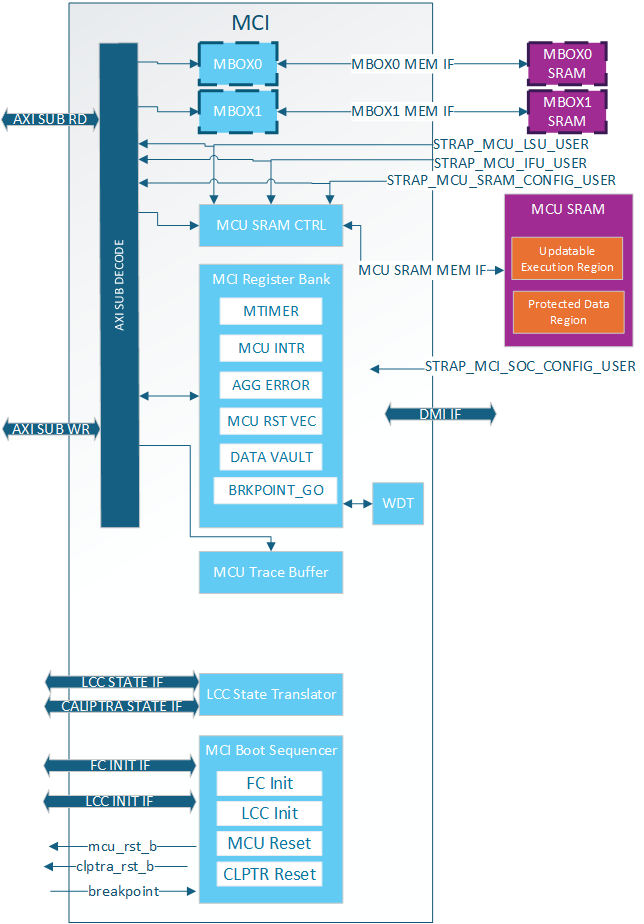
Parameters & Defines
Note: Additional parameter limitations can be seen in the Requirements section
Table: AXI Integration Parameters
| Facing | Parameter name | Location | Description |
|---|---|---|---|
| External | AXI_ADDR_WIDTH | mci_top | AXI address width |
| External | AXI_DATA_WIDTH | mci_top | AXI data width |
| External | AXI_USER_WIDTH | mci_top | AXI user width |
| External | AXI_ID_WIDTH | mci_top | AXI ID width |
Table: MCU SRAM Integration Parameters
| Facing | Parameter name | Location | Description |
|---|---|---|---|
| External | MCU_SRAM_SIZE_KB | mci_top | Size of MCU SRAM in KB. i.e. Min: 4 Max: 2048(2MB) |
Table: MCI Boot Sequencer Integration Parameters
| Facing | Parameter name | Location | Description |
|---|---|---|---|
| External | MIN_MCU_RST_COUNTER_WIDTH | mci_top | Size of MCU reset counter which determines the min reset time for the MCU. When the timer overflows MCU can be brought up. |
Table: MCI MBOX Integration Parameters
| Facing | Parameter name | Location | Description |
|---|---|---|---|
| External | MCU_SET_MBOX0_AXI_USER_INTEG | mci_top | Determines if VALID_AXI_USER will be used by MCI |
| External | MCU_MBOX0_VALID_AXI_USER | mci_top | MBOX0 AXI user list enabled by SET_MBOX0_AXI_USER_INTEG |
| External | MCU_MBOX0_SIZE_KB | mci_top | Size of MBOX0 SRAM. If set to 0 the entire MBOX0 is removed from MCI. Min: 0 Max: 2048 (2MB) |
| External | MCU_SET_MBOX1_AXI_USER_INTEG | mci_top | Determines if VALID_AXI_USER will be used by MCI |
| External | MCU_MBOX1_VALID_AXI_USER | mci_top | MBOX1 AXI user list enabled by SET_MBOX0_AXI_USER_INTEG |
| External | MCU_MBOX1_SIZE_KB | external | Size of MBOX1 SRAM. If set to 0 the entire MBOX1 is removed from MCI. Min: 0 Max: 2048 (2MB) |
Table: MCI Integration Definitions
| Defines | Defines file | Description |
|---|---|---|
| NONE DEFINED |
Interface
Note: Additional interface connection requirements/guidance can be seen in the Requirements section
Note: Any port listed as “STATIC” must be stable before mci_pwrgood is asserted. If the signal changes value after mci_pwrgood assertion will cause functional issues in MCI
Note: Internal means the signal is not directly exposed to the SOC. External means it is directly exposed for SOC to consume and connect.
Note: If a signal (like the clock) is combined with other IPs it is still listed as Ext.
Note: If a signal stays in the SS but will need SOC connection (AXI interfaces) due to the SS not instantiating a component (like an AXI interconnect) it is listed as Ext because the SOC will need to connect.
Note: Any port with known internal and external connections (i.e. agg_error_fatal) will have External/Internal with note in a different section on which ports are reserved for internal vs external use.
Table: MCI Clocks
| Facing | Type | Width | Name | Clock | Description |
|---|---|---|---|---|---|
| External | Input | 1 | clk | MCI Clock. Connected to subsystem top level clk input. | |
| External | Output | 1 | mcu_clk_cg | MCU clock gated when MCU in reset for RDC. Exposed as cptra_ss_mcu_clk_cg_o externally. | |
| External | Output | 1 | cptra_ss_rdc_clk_cg | MCI SS clock gated when caliptra reset asserted for RDC. Should be used whenever their is a Warm reset -> cold reset crossing in design. Must be paired with cptra_ss_rst_b_o reset for proper gating. Exposed to SOC as cptra_ss_rdc_clk_cg_o |
Table: MCI Resets
| Facing | Type | Width | Name | Description |
|---|---|---|---|---|
| External | Input | 1 | mci_pwrgood | Active high power good indicator. Deepest reset domain for MCI. |
| External | Input | 1 | mci_rst_b | Active low asynchronous reset for MCI. |
| External | Input | 1 | cptra_ss_rst_b_o | Active low asyn reset for Caliptra SS. Delayed version of mci_rst_b in order to gate cptra_ss_rdc_clk_cg and mcu_clk_cg before reset assertions for RDC purposes. When scan_mode is set, this is directly controlle by mci_rst_b |
| External | Output | 1 | mcu_rst_b | Reset for MCU. When scan_mode is set, this is directly controlled by mci_rst_b. Exposed as cptra_ss_mcu_rst_b_o externally. |
| External | Output | 1 | cptra_rst_b | Reset for Caliptra. When scan_mode is set, this is directly controlled by mci_rst_b. Exposed as cptra_ss_mci_cptra_rst_b_o externally. |
Table: MCI AXI Interface
| Facing | Type | Width | Name | Description |
|---|---|---|---|---|
| External | interface | s_axi_w_if | AXI subordinate write interface. Exposed to SOC as cptra_ss_mci_s_axi_if_w_sub | |
| External | interface | s_axi_r_if | AXI subordinate read interface. Exposed to SOC as cptra_ss_mci_s_axi_if_r_sub |
Table: MCI Straps
| Facing | Type | Width | Name | Description |
|---|---|---|---|---|
| External | Input | AXI_USER_WIDTH | strap_mcu_lsu_axi_user | AXI USER for MCU’s load/store unit. Exposed to SOC via cptra_ss_strap_mcu_lsu_axi_user_i |
| External | Input | AXI_USER_WIDTH | strap_mcu_ifu_axi_user | AXI USER for MCU’s instruction fetch unit. Exposed to SOC via cptra_ss_strap_mcu_ifu_axi_user_i |
| External | Input | AXI_USER_WIDTH | strap_mcu_sram_config_axi_user | AXI USER populating MCU FW Image in MCU SRAM. Exposed to SOC via cptra_ss_strap_mcu_sram_config_axi_user_i |
| External | Input | AXI_USER_WIDTH | strap_mci_soc_config_axi_user | AXI USER with MCU privilages in MCI reg. Use for Romless config. 0x0: Disable 0xFFFFFFFF: Debug (all AXI users get this privilage). Exposed to SOC via cptra_ss_strap_mci_soc_config_axi_user_i |
| External | Input | 32 | strap_mcu_reset_vector | Default reset vector for MCI. Can be overridden via MCI register write. Exposed to SOC via cptra_ss_strap_mcu_reset_vector_i |
| External | Input | 32 | ss_debug_intent | Debug intent |
Table: MCI CG Controls
| Facing | Type | Width | Name | Description |
|---|---|---|---|---|
| External | output | 1 | rdc_clk_dis | Clock disable for warm reset. Used to disable cptra_ss_rdc_clk_cg_o and cptra_ss_mcu_clk_cg_o clocks. Asserted a few clock cycles after cptra_ss_rst_b_i asserted and before cptra_ss_rst_b_o asserted. Deasserted a few clock cycles after cptra_ss_rst_b_i deasserted. Exposed as cptra_ss_warm_reset_rdc_clk_dis_o externally. |
| External | output | 1 | early_warm_reset_warn | Early reset warn used to change security related signals to a safe value before reset is asserted. Needed since Caliptra Core clock gating is slightly after MCI clock gating/reset assertion. Example is the security_state fed from MCI to Caliptra Core. Exposed as cptra_ss_early_warm_reset_warn_o externally |
| External | output | 1 | fw_update_rdc_clk_dis | Clock disable for MCU reset. Used to disable cptra_ss_mcu_clk_cg_o clock. Asserted a few clock cycles before cptra_ss_mcu_rst_b_o is asserted. Deasserted when MCI boot sequencer switches out of BOOT_RST_MCU state. Exposed as cptra_ss_mcu_fw_update_rdc_clk_dis_o externally |
Table: MCI MISC Interface
| Facing | Type | Width | Name | Description |
|---|---|---|---|---|
| Internal/External | input | 1 | mcu_sram_fw_exec_region_lock | FW_EXEC_CTRL[2] from Caliptra or SOC to indicate if there is a new MCU FW update avaialbe. Exposed to SOC as cptra_ss_cptra_generic_fw_exec_ctrl_2_mcu_i |
| External | input | 64 | mci_generic_input_wires | Generic input wires SOC can use to interrupt MCU. Exposed to SOC as cptra_ss_mci_generic_input_wires_i |
| External | output | 64 | mci_generic_output_wires | Generic output wires MCU can use to control SOC logic. Exposed to SOC as cptra_ss_mci_generic_output_wires_o |
| External | input | 1 | mcu_no_rom_config | 1: No rom config enabled 0: No rom config. Exposed to SOC as cptra_ss_mcu_no_rom_config_i |
Table: MCI MCU Interface
| Facing | Type | Width | Name | Description |
|---|---|---|---|---|
| Internal | output | 32 | mcu_reset_vector | MCU reset vector |
| Internal | output | 1 | mcu_cpu_halt_req_o | MCU halt request, used by MCI boot FSM. Exposed as ouput to SOC as cptra_ss_mcu_halt_req_o |
| Internal | input | 1 | mcu_cpu_halt_ack_i | MCU halt ack, used by MCI boot FSM. Exposed as output to SOC as cptra_ss_mcu_halt_ack_i |
| External/Internal | input | 1 | mcu_cpu_halt_status_i | MCU halt status, used by MCI boot FSM, and exposed as input to SOC as cptra_ss_mcu_halt_status_i |
| Internal | output | 1 | mcu_dmi_core_enable | MCU DMI Core Enable |
| Internal | output | 1 | mcu_dmi_uncore_enable | MCU DMI Uncore Enable |
| Internal | input | 1 | mcu_dmi_uncore_en | MCU DMI Uncore Interface Enable |
| Internal | input | 1 | mcu_dmi_uncore_wr_en | MCU DMI Uncore Interface Write Enable |
| Internal | input | 7 | mcu_dmi_uncore_addr | MCU DMI Uncore Interface Address |
| Internal | input | 32 | mcu_dmi_uncore_wdata | MCU DMI Uncore Interface Write Data |
| Internal | input | 32 | mcu_dmi_uncore_rdata | MCU DMI Uncore Interface Read Data |
| Internal | input | 1 | mcu_dmi_active | MCU DMI Interface Active |
| Internal | input | 1 | mcu_dmi_active | MCU DMI Interface Active |
| Internal | input | 32 | mcu_trace_rv_i_insn_ip | MCU trace instruction |
| Internal | input | 32 | mcu_trace_rv_i_address_ip | MCU trace address |
| Internal | input | 1 | mcu_trace_rv_i_valid_ip | MCU trace valid |
| Internal | input | 1 | mcu_trace_rv_i_exception_ip | MCU trace exception |
| Internal | input | 5 | mcu_trace_rv_i_ecause_ip | MCU trace exception cause |
| Internal | input | 1 | mcu_trace_rv_i_interrupt_ip | MCU trace interrupt |
| Internal | input | 32 | mcu_trace_rv_i_tval_ip | MCU trace exception trap value |
Table: MCI Errors and Interrupts Interface
| Facing | Type | Width | Name | Description |
|---|---|---|---|---|
| Internal/External | input | 32 | agg_error_fatal | Fatal errors from other Caliptra SS IPs or other SOC entities fed into MCI’s aggregate error infrastructure and will be reflected for SOC consumption via the all_error_fatal output wire of MCI |
| Internal/External | input | 32 | agg_error_non_fatal | Non-fatal errors from other Caliptra SS IPs or other SOC entities fed into MCI’s aggregate error infrastructure and will be reflected for SOC consumption via the all_error_non_fatal output wire of MCI. |
| External | Output | 1 | all_error_fatal | Fatal error interrupt for SOC consumption. Exposed as cptra_ss_all_error_fatal_o to SOC |
| External | Output | 1 | all_error_non_fatal | Non-fatal error interrupt for SOC consumption. Exposed as cptra_ss_all_error_non_fatal_o to SOC |
| Internal | Output | 1 | mcu_timer_int | MCU’s standard RISC-V MTIMER interrupt. |
| Internal | Output | 1 | mci_intr | MCI interrupt indication for MCU. This will be set when an unmasked interrupt occurs within MCI. This is a level interrupt and must be cleared by MCU firmware. |
| Internal | Output | 1 | nmi_intr | Non-maskable interrupt for MCU. This is connected to the watchdog (WDT) timer within MCI and will be asserted when the wdt is in cascade mode and both timers timeout. It can only be cleared by asserting mci_rst_b. This interrupt is also fed into the all_error_fatal infrastructure for SOC consumption. |
| Internal | Output | 32 | mci_nmi_vector | Non-maskable interrupt vector for MCU. This is controllable only by MCU FW. |
| Internal | input | 1 | cptra_mbox_data_avail | Cptra mailbox data is available for SOC/MCU. Fed into MCI interrupts for MCU. |
| Internal | input | 1 | intr_otp_operation_done | FC OTP operation done interrupt fed into MCI interrupts for MCU. |
| Internal | output | 1 | soc_mcu_mbox0_data_avail | MCU MBOX0 data available for SOC. |
| Internal | output | 1 | soc_mcu_mbox1_data_avail | MCU MBOX0 data available for SOC. |
Table: MCI LCC Bring Up Interface
| Facing | Type | Width | Name | Description |
|---|---|---|---|---|
| Internal | Input | 1 | lc_done | LCC initialization done response used by MCU boot sequencer to move to the next state. |
| Internal | Output | 1 | lc_init | LCC initialization request asserted by the MCU boot sequencer after every MCI reset. |
Table: MCI FC Bring Up Interface
| Facing | Type | Width | Name | Description |
|---|---|---|---|---|
| Internal | Input | 1 | fc_opt_done | FC initialization done response used by MCU boot sequencer to move to the next state. |
| Internal | Output | 1 | fc_opt_init | FC initialization request asserted by the MCU boot sequencer after every MCI reset. |
Table: MCU SRAM Interface
| Facing | Type | Width | Name | Description |
|---|---|---|---|---|
| External | interface | mci_mcu_sram_req_if | Data width is DATA+ECC. Address width shall be wide enough to address entire SRAM. | MCU SRAM memory interface. |
| External | interface | mci_mbox0_sram_req_if | Data width is DATA+ECC. Address width shall be wide enough to address entire SRAM. | MBOX0 SRAM memory interface. |
| External | interface | mci_mbox1_sram_req_if | Data width is DATA+ECC. Address width shall be wide enough to address entire SRAM. | MBOX1 SRAM memory interface. |
Table: MCI LCC Gasket Interface
| Facing | Type | Width | Name | Description |
|---|---|---|---|---|
| Internal | Input | Struct | from_lcc_to_otp_program_i | These are the LCC port lists that program corressponding fuse partition for LCC |
| Internal | Input | Struct | lc_dft_en_i | LCC decoding signal, see LCC section |
| Internal | Input | Struct | lc_hw_debug_en_i | LCC decoding signal, see LCC section |
| Internal | Input | Struct | from_otp_to_lcc_program_i | These ports comes from fuse partitions and show LCC's non-volatile state |
| Internal | Input | 1 | ss_dbg_manuf_enable_i | Caliptra Core enables manuf debug with this |
| Internal | Input | 64 | ss_soc_dbg_unlock_level_i | Caliptra Core enables prod debug with this. Since there are multiple debug levels, the debug level is one-hot encoded to this port |
| External | Output | 1 | SOC_DFT_EN | Masked LCC decoding signal, see LCC section |
| External | Output | 1 | SOC_HW_DEBUG_EN | Masked LCC decoding signal, see LCC section |
| Internal | Output | Struct | security_state_o | Caliptra Core's security state |
| External | Input | 1 | FIPS_ZEROIZATION_PPD_i | Physical pin to trigger zeroization |
| Internal | Output | 1 | FIPS_ZEROIZATION_CMD_o | Masked zeroization command signal |
Memory Map / Address map
Top Level Memory Map
| Internal Block | Address Offset (from base address) | End Address |
|---|---|---|
| CSRs | 0x0 | 0x1FFF |
| MCU Trace Buffer | 0x10000 | 0x1001F |
| Mailbox 0 | 0x400000 | 0x7FFFFF |
| Mailbox 1 | 0x800000 | 0xBFFFFF |
| MCU SRAM | 0xC00000 | MCU SRAM BASE + MCU_SRAM_SIZE |
MCU SRAM Memory Map
MCU SRAM is split into 2 sections:
- Updatable Execution Region
- Protected Data Region
The two regions have different access protection. The size of the regions is dynamically changed via the FW_SRAM_EXEC_REGION_SIZE register in 4KB increments.
Table: MCU SRAM Regions
| MCU SRAM Region | Address Start Offset |
|---|---|
| Updatable Execution Region | 0x0 |
| Protected Region | FW_SRAM_EXEC_REGION_SIZE * 1024 * 4 |
NOTE: FW_SRAM_EXEC_REGION_SIZE is base 0 meaning the minimum size for the Updatable Execution Region is 4KB.
NOTE: If FW_SRAM_EXEC_REGION_SIZE is the size of the SRAM, there is no protected Region.
MCI Integration Requirements
-
Connectivity, Clock & Reset, Constraints & Violations etc
-
AXI Parameters and AXI Interface Parameter Alignment
Due to SystemVerilog limitations MCI exposed both AXI parameters and AXI interfaces that are parameterized. Parameters between all AXI interface and the MCI AXI parameters must be consistent.
-
AXI DATA_WIDTH Limitation
MCI DATA_WIDTH was only verified with a value of 32. If a different width is required the user will have to make internal MCI changes and no functionality is guaranteed.
-
AXI ADDR_WIDTH Limitation
AXI ADDR_WIDTH must be wide enough to fully address the MCI address space.
-
MCI Base Address Requirement
The base address assigned to MCI must align to the MCI total addressable space. This can be calculated based off of the MCU SRAM size since it is the last block in the MCI memory map.
To calculate the base address alignment use the following calculation:
bits = $clog2(MCU_SRAM_OFFSET + ((MCU_SRAM_SIZE_KB * 1024) - 1))MCU_SRAM_OFFSET can be found in the MCI’s Top Level Memory Map.
Example:
MCU_SRAM_OFFSET = 0xC00000 (12582912 decimal) MCU_SRAM_SIZE_KB = 512 (512KB) bits = $clog2(12582912 + ((512 * 1024) - 1)) bits = 24 MCI base address would need to align to 0x80_0000 -
Reset Synchronization
MCI does not synchronize any resets inside the IP. It is expected all reset inputs are properly synchronized to the MCI clock domain before being passed to MCI.
All MCI reset outputs are synchronous to the MCI clock domain and if they are used in a different clock domain they shall be properly synchronized outside of MCI.
-
DFT Reset Control
MCI input resets do not have any built-in DFT reset control for scan. It is the integrator’s responsibility to add any DFT controls outside of MCI before the reset is connected to MCI.
Simlar to Caliptra core - When
scan_modeis set the MCI generated resets will be directly controlled bymci_rst_b. This gives DFT complete control of these resets within Caliptra SS. -
Integrator RTL modification requirements
MCI reused synchronizer modules from Caliptra Core like caliptra_2ff_syn.sv. Integrators are required to replace these modules with technology-specific sync cells.
MCI does not itself contain modules that need to be directly modified by the integrator.
-
Late Binding interface signals
The interface signals
mci_generic_input_wiresandmci_generic_output_wiresare placeholders on the SoC interface reserved for late binding features. This may include any feature that is required for correct operation of the design in the final integrated SoC and that may not be accommodated through existing interface signaling (such as the mailbox).Each wire connects to a register in the MCI register bank through which communication to the MCU may be facilitated. Each of the generic wire signals is 64 bits in size.These signals are considered ASYNC and each of the 64 bits are considered separate adhoc signals. Meaning there is no bus synchronization which means the connections to this port need to be thoroughly thought through to ensure the MCU doesn’t drop any requests.
Activity on any bit of the
mci_generic_input_wirestriggers a notification interrupt to the microcontroller indicating a bit toggle.The following tables describe the allocation of functionality on
mci_generic_input_wiresandmci_generic_output_wires. Bits not assigned to a function can be used by the SOC for their own needs. These generic wires could be reserved by CHIPS Alliance in future Caliptra drops. Any unused inputs shall be tied off to 0 and outputs left unconnected.Table: MCI Generic Input Allocation
-
| Bits | Name | Description |
|---|---|---|
| 63:1 | RESERVED | No allocated function |
| 0 | FIPS_ZEROIZATION_PPD_i | FIPS zeroization request sampled by MCU ROM. If FIPS zeroization is required, this signal shall be set before Caliptra SS is out of reset. If set, MCU ROM will set MASK register triggering FIPS zeroization flow. If this signal is toggled at runtime it shall be ignored. |
**Table: MCI Generic Output Allocation**
| Bits | Name | Description |
|---|---|---|
| 63:0 | RESERVED | No allocated function |
Error Aggregation Connectivity Requirements
MCI aggregates all fatal and non-fatal errors for Caliptra SS via two ports agg_error_fatal and agg_error_non_fatal. These errors are:
- Sent to MCU via interrupt
- Sent to SOC via
all_error_fatalorall_error_non_fatalMCI output ports
Errors connected to this infrastructure are required to be level signals. Pulses are not permitted.
MCU has the ability to independently mask these aggregated interrupts to its own interrupt and to the all_error_fatal and all_error_non_fatal output ports.
Aggregate error connections can be see in Caliptra SS HW Spec: MCI Error Handling.
Subsystem Internal Fuse Controller Initialization Connectivity Requirements
During Caliptra SS bring up the MCI handshakes with the FC to do initialization. The flow is:
- MCI: Assert lc_init
- FC: Assert lc_done
Connections between MCI and FC are shown in the table below:
Table: MCI to FC Init Connections
| MCI Port | FC Port |
|---|---|
| fc_opt_init | pwr_otp_i.otp_init |
| fc_opt_done | pwr_otp_o.otp_done |
Subsystem Internal Life Cycle Controller Initialization Connectivity Requirements
During Caliptra SS bring up the MCI handshakes with the LCC to do initialization. The flow is:
- MCI: Assert fc_opt_init
- FC: Assert fc_opt_done
Connections between MCI and LCC are shown in the table below:
Table: MCI to LCC Init Connections
| MCI Port | FC Port |
|---|---|
| lc_init | pwr_lc_i.lc_init |
| lc_done | pwr_lc_o.lc_done |
MCI MCU Connectivity Requirements
The table below shows connections between MCI and MCU that are not part of other features:
Table: MCI to MCU Connections
| MCI Port | Direction | MCU Port | Description |
|---|---|---|---|
| mcu_reset_vector | -> | rst_vec | Reset vector for MCU |
| nmi_intr | -> | nmi_intr | WDT interrupt for MCU |
| mcu_nmi_vector | -> | nmi_vec | MCU nonmaskable interrupt vector |
| mcu_rst_b | -> | rst_l | MCU reset |
MCI Caliptra Core Connectivity Requirements
The table below shows connections between MCI and Caliptra Core that are not part of other features:
Table: MCI to Caliptra Core Connections
| MCI Port | Direction | Caliptra Port | Description |
|---|---|---|---|
| mcu_sram_fw_exec_region_lock | <- | ss_generic_fw_exec_ctrl[2] | Controls MCU SRAM protection and used to bring MCU into reset for hitless match. NOTE: connection is looped by SOC at top level allowing SOC to use their own register to control this input. This is needed if Caliptra is not used. |
| cptra_rst_b | -> | cptra_rst_b | Reset for Caliptra. NOTE: Connection is looped by SOC at top level allowing for SOC to keep Caliptra in reset if not needed. |
LCC Gasket Connectivity Requirements
Below are the connections needed between MCI and LCC for the Gasket functionality
Table: LCC Gasket - MCI to LCC Connections
| MCI Port | Direction | LCC Port | Description |
|---|---|---|---|
| from_lcc_to_otp_program_i | <- | lc_otp_program_o | See LCC Section |
| lc_dft_en_i | <- | lc_dft_en_o | See LCC Section |
| lc_hw_debug_en_i | <- | lc_hw_debug_en_o | See LCC Section |
| from_otp_to_lcc_program_i | <- | otp_lc_data_i | See LCC Section |
Table: LCC Gasket - MCI to Caliptra Core Connections
| MCI Port | Direction | Caliptra Core Port | Description |
|---|---|---|---|
| ss_dbg_manuf_enable_i | <- | ss_dbg_manuf_enable | See Caliptra Integration spec |
| ss_soc_dbg_unlock_level_i | <- | ss_soc_dbg_unlock_level | See Caliptra Integration spec |
| security_state_o | -> | security_state | See LCC state tranlation table |
Table: LCC Gasket - MCI to Caliptra SS Port Connections
| MCI Port | Direction | SS Port | Description |
|---|---|---|---|
| SOC_DFT_EN | -> | cptra_ss_soc_dft_en_o | SOC DFT enable see DFT LC States |
| SOC_HW_DEBUG_EN | -> | cptra_ss_soc_hw_debug_en_o | SOC HW Debug Enable see: DFD LC States |
Table: Fuse Zeroization Signals - Caliptra SS Port Connections to MCI to FC
| MCI Port | Direction | SS Port | FC Port | Description |
|---|---|---|---|---|
| FIPS_ZEROIZATION_PPD_i | <- | cptra_ss_FIPS_ZEROIZATION_PPD_i | - | Zeroization enable see Zeroization Process |
| FIPS_ZEROIZATION_CMD_o | -> | - | FIPS_ZEROIZATION_CMD_i | Zeroization enable see Zeroization Process |
MCU SRAM Sizing Requirements
MCU SRAM size is set via the MCU_SRAM_SIZE_KB parameter.
The minimum size supported is 4KBs.
The maximum size supported is 2MBs.
It is suggested the size is on a 4KB boundary since the split between the execution region and secure region is done via MCI CSR in 4KB increments.
Standard size is 512KB.
The size of the SRAM should be determined based on:
- MCU runtime image size
- STACK
- Large data structures or persistent logs maintained by MCU
- .data/.bss sections
- Any other data MCU plans on storing the the MCU SRAM.
Storage guidance for Execution vs Protected region are as follows:
- Execution
- Executable Runtime Instructions for MCU
- .data/.bss sections
- STACK
- Protected
- STACK
- Incorruptible data structures
- Persistent logs maintained by MCU
Access to MCU SRAM Execution Region is controlled by mcu_sram_fw_exec_region_lock. Before MCU is brought out of reset for a hitless patch this signal must be asserted giving access to the MCU. Failure to do so will trigger an AXI access error since Caliptra will be the only entity allowed to access the SRAM until this signal is asserted.
MCU MBOX SRAM Sizing Requirements
MCU MBOX SRAM size is set via MCU_MBOX0_SIZE_KB and MCU_MBOX1_SIZE_KB parameters
The MCU can be configured to implement up to 2 independent mailboxes with maximum fully addressable SRAM. sizes of up to 2 MB. If they are configured sizes of 0, they will not be instantiated.
Size should be determined by:
- Max MCU FW image size
- Max size of other FW images Caliptra SS will handle
Programming interface
MCI Register Spec
MCU Mailbox
Each mailbox can be used for secure and restricted communication between external SoC entities, the MCU, and Caliptra core. This communication channel is essential for exchanging control messages, status updates, and other critical information that the MCU will use to monitor system boot, firmware updates, and security critical operations. Mailboxes are designed to ensure that only authorized entities can access and communicate through it, preserving the integrity and security of the SoC operations.
The mailboxes are generic with some specific protocols and legal operations/accesses to ensure their secured and restricted aspect. The command, statuses, and data that are intepreted by the MCU microcontroller (uC), Caliptra uC or other SoC agent are not defined or enforced in this specification.
Since the MCU uC has root access to the mailboxes (even when the mailbox is locked), it can function as an intermediary and facilitate communication between 2 agents (such as Caliptra uC and other SoC agents).
The Caliptra SS HW MCU Mailbox Spec has more details about the specific registers and interrupts used in the mailbox flows.
MCU Mailbox Limited Trusted AXI users
If build-time integration straps are not used for configuring the trusted MBOX AXI users, then trusted users will need to configured with the following lockable MCI registers before MBOX can be used by SOC agents:
MBOX*_VALID_AXI_USERMBOX*_AXI_USER_LOCK
See Caliptra SS MCU Trusted AXI Users for more details.
Reset
The mailboxes start locked by MCU to prevent any data leaks across warm reset. MCU shall set MBOX_DLEN to MBOX SRAM size and write 0 to MBOX_EXECUTE to release the MBOX and wipe the MBOX SRAM. This should be done before using or allowing use of the mailboxes.
MCU Mailbox Doorbell Command DLEN
An MBOX doorbell command has no data. When MBOX_DLEN = 0 and MBOX_EXECUTION is cleared, the clearing logic erases the entire MBOX SRAM. To avoid long delays caused by this clearing, firmware should set MBOX_DLEN = 1 when issuing doorbell commands.
MCI Debug Lock Status
MCI exposed the debug state of the chip to MCU via an interrupt notif_debug_locked_sts and a status register SECURITY_STATE.debug_locked. There is no defined use case for this feature at subsystem level, unlike in Caliptra where security assets are cleared when entering debug locked state. Therefore, it is recommended this interrupt remains disabled using notif_debug_locked_en.
If there is a need to use debug state the recommened flow to avoid missing a debug locked transition is:
- Out of reset MCU W1C
notif_debug_locked_sts - MCU reads
SECURITY_STATE.debug_lockedand acts on the value seen - MCU enables the interrupt using
notif_debug_locked_en
MCU to SOC Receiver Flow
- MCU attempts to lock mailbox by reading
MBOX_LOCKregister
- If read returns 0, LOCK is granted and will be set to 1
- If read returns 1, MBOX is locked for another agent
- MCU writes data to
MBOX_SRAM - MCU writes data length in bytes to
MBOX_DLEN - MCU writes command to
MBOX_CMDregister - MCU sets
MBOX_TARGET_USERto SOC Receiver AXI and sets MBOX_TARGET_USER_VALID to 1 - MCU writes 1 to
MBOX_EXECUTEregister (which asserts cptra_ss_soc_mcu_mbox*_data_avail output) - MCU can directly inform receiver depending on receiver capabilities OR receiver could use cptra_ss_soc_mcu_mbox*_data_avail wire to directly generate an interrupt
- Receiver processes command and data in mailbox
- Receiver updates
MBOX_SRAMandMBOX_DLEN(if there is data to return). - Reciever updates status in
MBOX_TARGET_STATUS.STATUSand setsMBOX_TARGET_STATUS.DONE
- This generates interrupt MBOX*_TARGET_DONE to MCU
- MCU (in response to MBOX*_TARGET_DONE interrupt) will write 0 to
MBOX_EXECUTEto release the MBOX - MCI clears MBOX CSRs and zeros out data from 0 to the max DLEN set during the whole lock session in
MBOX_SRAM
- Mailbox lock cannot be re-acquired until zeroization is complete
SOC Sender to MCU Flow
- Sender attempts to lock mailbox by reading
MBOX_LOCKregister
- If read returns 0, LOCK is granted and will be set to 1
- If read returns 1, MBOX is locked for another agent
- Sender writes data to
MBOX_SRAM - Sender writes data length in bytes to
MBOX_DLEN - Sender writes command to
MBOX_CMDregister - Sender writes 1 to
MBOX_EXECUTEregister
- This generates MBOX*_CMD_AVAIL interrupt to MCU
- MCU processes command and data in mailbox
- MCU updates
MBOX_SRAMandMBOX_DLEN(if there is data to return). - MCU update
MBOX_CMD_STATUSwith desired status code - Sender writes 0 to
MBOX_EXECUTEto release the MBOX - MCI clears MBOX CSRs and zeros out data from 0 to the max DLEN set during the whole lock session in
MBOX_SRAM
- Mailbox lock cannot be re-acquired until zeroization is complete
SOC Sender to SOC Receiver Communication Flow (MCU as intermediary)
- Sender attempts to lock mailbox by reading
MBOX_LOCKregister
- If read returns 0, LOCK is granted and will be set to 1
- If read returns 1, MBOX is locked for another agent
- Sender writes data to
MBOX_SRAM - Sender writes data length in bytes to MBOX_DLEN
- Sender writes command to
MBOX_CMDregister - Sender writes 1 to
MBOX_EXECUTEregister
- This generates MBOX*_CMD_AVAIL interrupt to MCU
- Sender reads/polls
MBOX_CMD_STATUSfor desired completion/ready status - MCU (in response to MBOX*_CMD_AVAIL interrupt) processes command and data
- MCU sets
MBOX_TARGET_USERto SOC Receiver AXI and sets MBOX_TARGET_USER_VALID to 1 - MCU notifies SOC Receiver they can access MBOX (method depends on SOC Receiver capabilities)
- Receiver reads MBOX and processes command and/or data
- Receiver potentially updates data in
MBOX_SRAMandMBOX_DLEN - Reciever updates status in
MBOX_TARGET_STATUS.STATUSand setsMBOX_TARGET_STATUS.DONE
- This generates interrupt MBOX*_TARGET_DONE to MCU
- MCU (in response to MBOX*_TARGET_DONE interrupt) will update
MBOX_CMD_STATUSwith final status - Sender sees final desired
MBOX_CMD_STATUS - Sender writes 0 to
MBOX_EXECUTEto release the MBOX - MCI clears MBOX CSRs and zeros out data from 0 to the max DLEN set during the whole lock session in
MBOX_SRAM
- Mailbox lock cannot be re-acquired until zeroization is complete
MCU JTAG/DMI Access
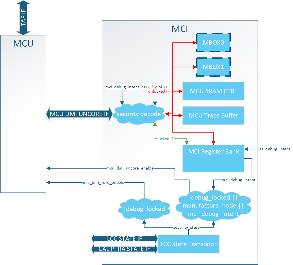
MCI provides access JTAG security for MCU. Detailed debug architecture can be found in MCI debug spec. Some notes about MCI debug arcitecture:
- MCI registers are accessed via the MCU DMI uncore address space.
- Limited MCU JTAG access is provided to MCI DMI registers by setting
cptra_ss_debug_intent_i - Full access to MCU core and uncore DMI registers is restricted to LCC unlocked mode.
MCU SRAM JTAG Access
MCU SRAM is fully accessable via MCU JTAG. MCU must be halted before accessing MCU SRAM via JTAG otherwise collisions between AXI and JTAG will result in errors and corrupted data.
MCU Trace Buffer
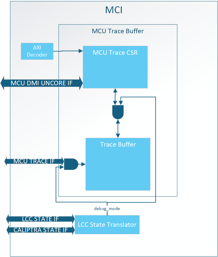
MCI hosts the MCU trace buffer. The full trace buffer spec is here. High level notes about trace buffer:
- It can only be accessed when debug unlocked
- It can be accessed via AXI or DMI
- Traces can be disabled via a RISC-V control register
- Traces are sticky and persist through warm reset
- The trace buffer can hold a total of 64 traces
MCU Halt Ack Interface
Caliptra SS exposed the MCU halt ack handshake to enable MCU No Rom Config.
If the SOC does not support MCU No Rom Config Caliptra SS requires the signals to be looped back.
| Caliptra SS port | Direction | Connection |
|---|---|---|
cptra_ss_mcu_halt_status_o | output | cptra_ss_mcu_halt_status_i |
cptra_ss_mcu_halt_status_i | input | cptra_ss_mcu_halt_status_o |
cptra_ss_mcu_halt_ack_o | output | cptra_ss_mcu_halt_ack_i |
cptra_ss_mcu_halt_ack_i | input | cptra_ss_mcu_halt_ack_o |
cptra_ss_mcu_halt_req_o | output | Unused by SOC |
If the SOC supports MCU No Rom Config the SOC must drive the halt_ack/status during the first Caliptra SS boot out of Cold Reset since MCU is still in reset. It shall give control back to MCU after it has completed the initial halt handshake as specified in MCU No ROM Config flow. The recommended connections if MCU No Rom Config is supported:
| Caliptra SS port | Direction | Connection |
|---|---|---|
cptra_ss_mcu_halt_status_o | output | cptra_ss_mcu_halt_status_i |
cptra_ss_mcu_halt_status_i | input | cptra_ss_mcu_halt_status_o ORed with SOC control |
cptra_ss_mcu_halt_ack_o | output | cptra_ss_mcu_halt_ack_i |
cptra_ss_mcu_halt_ack_i | input | cptra_ss_mcu_halt_ack_o ORed with SOC control |
cptra_ss_mcu_halt_req_o | output | Used to enable/disable the SOC control of ack/status |
Sequences : Reset, Boot,
MCI Boot Sequencer
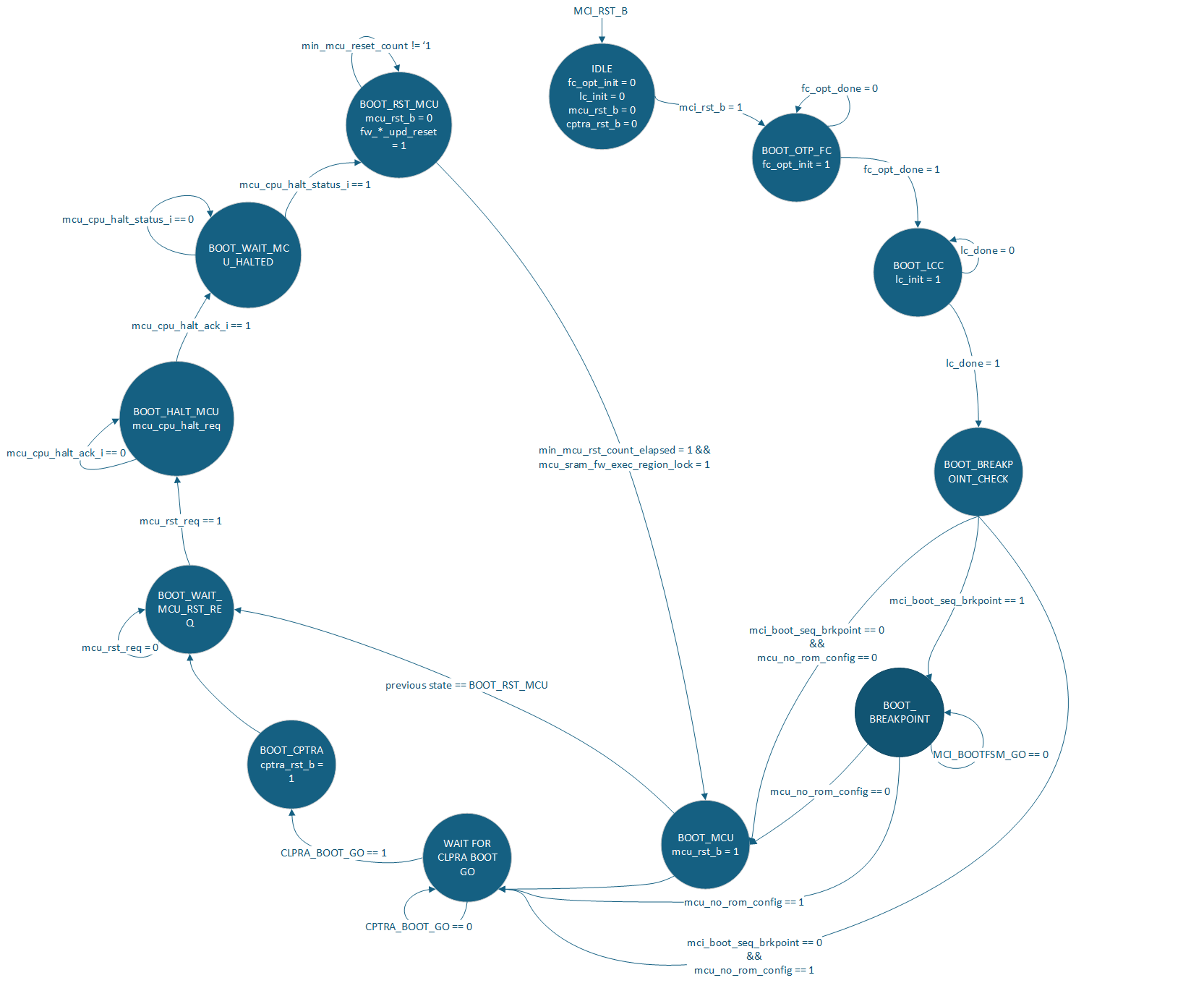
The MCI is responsible for bringing up the Caliptra SS. This is done via the MCI Boot Sequencer. The primary job of this FSM is to:
- Initialize the fuse controller
- Initialize the life cycle controller
- Allow a breakpoint for debug intervention before MCU or Caliptra are out of reset
- Bring MCU out of reset
- Bring Caliptra out of reset
- Control MCU reset for hitless updates
Breakpoint Flow
The SOC can halt the MCI Boot Sequencer via the mcu_boot_seq_brkpoint port. When set to 1 it will cause the MCI Boot Sequence to halt after it has initialized both FC and LCC.
This port shall be set and stable before mcu_rst_b is deasserted. Failure to do so will mean the breakpoint might be missed by MCI Boot Sequencer.
Once in BOOT_BREAKPOINT a user can use MCU JTAG to configure MCI other components within the Caliptra SS for debug.
One known usecase for the breakpoint is to bypass the ROM and jump to a debug image in MCU SRAM.
To proceed after a breakpoint the SOC must write the MCI_BOOTFSM_GO.go register via AXI or MCI DMI port.
MCU No ROM Config
Caliptra SS supports booting without a MCU ROM. To enable this configuration the SOC must:
cptra_ss_mcu_no_rom_config_iset to 1cptra_ss_strap_mci_soc_config_axi_user_iset to a trusted user other than MCUcptra_ss_mcu_halt_status_iconnected tocptra_ss_mcu_halt_status_oORed with SOC controlcptra_ss_mcu_halt_ack_iconnected tocptra_ss_mcu_halt_ack_oORed with SOC control- (optional)
cptra_ss_strap_mcu_reset_vector_iset to known starting address in MCU SRAM
The expected boot sequence is:
- MCI brought out of reset
- MCI boot FSM progresses to
WAIT_FOR_CPTRA_BOOT_GO - Trusted SOC agent does configuration MCU ROM typically executes. See CSS HW spec
- Trusted SOC agent sets
CPTRA_BOOT_GO.gobringing Caliptra out of reset - Trusted SOC agent executes MCU FW Boot Update with Caliptra
- When SOC agent sees
notif_cptra_mcu_reset_req_stsset by Caliptra, SOC will seecptra_ss_mcu_halt_req_oasserted by MCI Boot FSM. SOC must assertcptra_ss_mcu_halt_status_iandcptra_ss_mcu_halt_ack_iback to MCI. When SOC seescptra_ss_mcu_halt_req_odeassert SOC shall give full control of these signals back to MCU. - See MCU Halt Ack Interface for recommended connections.
During step 5 MCU will be brought out of reset and start executing from MCU SRAM.
No Caliptra Core Config
If an SOC does not need Caliptra and wants to use a different entity to service MCU FW updates the SOC can:
- Tie
cptra_ss_rst_b_ito 0 - Leave
cptra_ss_rst_b_ounused - Set
cptra_ss_strap_mcu_sram_config_axi_user_ito a trusted user- Gives SOC agent access to MCU SRAM allowing it to populate it with a FW image.
cptra_ss_cptra_generic_fw_exec_ctrl_2_mcu_icontrolled by the trusted user instead of Caliptra- Gives SOC agent reset request control of MCU.
- Leave
cptra_ss_cptra_generic_fw_exec_ctrl_2_mcu_ounused
Connectivity requirements can be found in FW Execution Control Connections and Caliptra Core Reset Control
Reset Ordering
The following table defines the order in which resets can get asserted. A ">>" in a cell at row X and column Y indicates that if the reset in row X is asserted, the reset in row Y is also asserted. For the rest of the cells (in which symbol ">>" is not present) the preceding assumption is not true and so the paths between those resets are potential RDC violations. The "N/A" cells are ignored because they are between the same resets.
Table: MCI Reset Ordering
| mci_pwrgood | mci_rst_b | mcu_rst_b | cptra_rst_b | |
|---|---|---|---|---|
| mci_pwrgood | N/A | >> | >> | >> |
| mci_rst_b | N/A | >> | >> | |
| mcu_rst_b | N/A | |||
| cptra_rst_b | N/A |
MCU FW Update Flows
The hitless flow is described in full in Caliptra Top Spec. The Caliptra SS HW Spec spec gives details about the registers used in theese flow. This section is meant to elaborate on how to use the given HW to meet the architectual spec.
Registers relevant to these flows:
- Caliptra
SS_GENERIC_FW_EXEC_CTRL[0].go[2]
- MCI
RESET_STATUS.mcuMCU_RESET_REQRESET_REASONnotif_cptra_mcu_reset_req_sts
MCU FW Boot Update
First MCU FW Update after a Cold Reset.
- Out of Cold Boot Caliptra has access to MCU SRAM since
FW_EXEC_CTRL[2]is reset to 0. - MCU ROM should use
notif_cptra_mcu_reset_req_stsinterrupt to know when Caliptra has a FW image for MCU. MCU ROM can either poll or enable the interrupt. - Caliptra sets MCI's
RESET_REASON.FW_BOOT_UPD_RESETand Caliptra'sFW_EXEC_CTRL[2]indicating a FW image is ready for MCU in MCU SRAM. - MCU sees request from Caliptra and shall clear the interrupt status.
- MCU sets
RESET_REQUEST.mcu_reqin MCI to request a reset. - MCI does an MCU halt req/ack handshake to ensure the MCU is idle
- MCI asserts MCU reset (min reset time for MCU is until MIN_MCU_RST_COUNTER overflows)
- MCU is brought out of reset and checks MCI's
RESET_REASON - MCU jumps to MCU SRAM
MCU Hitless FW Update
Subsequent MCU FW Update after FW Boot Update.
- MCU FW should use
notif_cptra_mcu_reset_req_stsinterrupt to know when Caliptra has a FW image for MCU. MCU FW can either poll or enable the interrupt. - Caliptra clears
FW_EXEC_CTRL[2]indicating a FW image is ready for MCU. - MCU sees request from Caliptra and shall clear the interrupt status.
- MCU sets
RESET_REQUEST.mcu_reqin MCI to request a reset. - MCI does an MCU halt req/ack handshake to ensure the MCU is idle
- MCI asserts MCU reset (min reset time for MCU is until MIN_MCU_RST_COUNTER overflows)
- Caliptra will wait until
RESET_STATUS.MCU_RESET_STSis set to indicate that reset is complete. - Caliptra will then have access to MCU SRAM Updatable Execution Region and update the FW image.
- Caliptra sets
RESET_REASON.FW_HITLESS_UPD_RESET - Caliptra sets
FW_EXEC_CTRL[2] - MCU is brought out of reset and checks MCI's
RESET_REASON - MCU jumps to MCU SRAM
MCU Warm Reset FW Update
Caliptra SS reset toggle without powergood toggle.
IMPORTANT - Can only happen after both Caliptra Core and MCU have loaded mutable firmware. Otherwise only Cold Reset is allowed.
- MCU ROM comes out of reset and sees
WARM_RESET. It cannot jump to MCU SRAM since it is locked and needs Caliptra to unlock. - MCU ROM brings Caliptra out of reset
- Caliptra sees Warm Reset and starts executing from its ICCM (SRAM image)
- Caliptra clears MCI's
RESET_REASON.WARM_RESETand setsRESET_REASON.FW_BOOT_UPD_RESET - Caliptra sets
FW_EXEC_CTRL[2] - MCU sees request from Caliptra and shall clear the interrupt status.
- MCU sets
RESET_REQUEST.mcu_reqin MCI to request a reset. - MCI does an MCU halt req/ack handshake to ensure the MCU is idle
- MCI asserts MCU reset (min reset time for MCU is until MIN_MCU_RST_COUNTER overflows)
- MCU is brought out of reset and checks MCI's
RESET_REASON - MCU jumps to MCU SRAM
Error Flows
- Example all_error_fatal Flow
Below is an example flow an SOC can follow that would properly clear all interrupts for all_error_fatal:
Setup assumes all interrupts to MCU and all_error_fatal are enabled via MCI CSRs
- agg_error_fatal bit 0 is asserted by an IP
- error_agg_error_fatal0_sts for MCU will be asserted
- agg_error_fatal0 for SOC all_error_fatal will be asserted
- MCU:
- Interrupted via mci_intr
- Takes action on error
- This could just be a loop waiting for a reset as fatal errors typically need a system wide reset.
- Waits for interrupt source to be cleared see SOC steps
- W1C error_agg_error_fatal0_sts to clear the interrupt
- SOC:
- Interrupted via all_error_fatal
- Takes action on error
- Could be logging or resetting of the SOC
- Clears the source of the error causing agg_error_fatal[0] to be cleared
- W1C agg_error_fatal0
- At this point all interrupt registers within MCI register bank are cleared but all_error_fatal is still asserted.
- Reset MCI via mci_rst_b
- Clears the all_error_fatal output port
- Example all_error_non_fatal Flow
Below is an example flow an SOC can follow that would properly clear all interrupts for all_non_error_fatal:
Setup assumes all interrupts to MCU and all_error_non_fatal are enabled via MCI CSRs
- agg_error_fatal bit 0 is asserted by an IP
- notif_agg_error_fatal0_sts for MCU will be asserted
- agg_error_non_fatal0 for SOC all_error_non_fatal will be asserted
- MCU:
- Interrupted via mci_intr
- Takes action on error
- Could just be a logging of the non-fatal error
- Waits for interrupt source to be cleared see SOC steps
- W1C notif_agg_error_fatal0_sts to clear the interrupt
- SOC:
- Interrupted via all_error_non_fatal
- Takes action on error
- Could be logging or resetting of the SOC
- Clears the source of the error causing agg_error_non_fatal[0] to be cleared
- W1C agg_error_non_fatal0
- Once MCU and SOC have finished their flows all interrupts will be cleared
See MCI error handling for more details on MCI error infrastructure.
Other requirements
I3C core
Overview
The I3C core in the Caliptra Subsystem is an I3C target composed of two separate I3C targets:
- Main target : Main target is responsible for any flows other than recovery or streaming boot.
- Recovery target : Recovery target is dedicated to streaming boot / recovery interface.
- This I3C code integrates with an AXI interconnect, allowing AXI read and write transactions to access I3C registers. For details on the core’s internal registers and functionality, see:
Integration Considerations
- Connections
- Connection to AXI interface
- GPIO connection to I3C Host (VIP or RTL)
Parameters and defines
| Parameter/Define | Default Value | Description |
|---|---|---|
AxiDataWidth | `AXI_DATA_WIDTH | Width (in bits) of the AXI data bus |
AxiAddrWidth | `AXI_ADDR_WIDTH | Width (in bits) of the AXI address bus |
AxiUserWidth | `AXI_USER_WIDTH | Width (in bits) of the AXI user signals |
AxiIdWidth | `AXI_ID_WIDTH | Width (in bits) of the AXI ID signals |
DatAw | i3c_pkg::DatAw | Data address width (defined in i3c_pkg) |
DctAw | i3c_pkg::DctAw | Device context address width (i3c_pkg) |
CsrAddrWidth | I3CCSR_pkg::I3CCSR_MIN_ADDR_WIDTH | CSR address width (defined in I3CCSR_pkg) |
CsrDataWidth | I3CCSR_pkg::I3CCSR_DATA_WIDTH | CSR data width (defined in I3CCSR_pkg) |
DISABLE_INPUT_FF | Not Defined | DO NOT DEFINE. NO LONGER VALID CONFIG. If defined will remove synchronizer on SCL input signal causing CDC issue. |
Interface
| Signal | Direction | Width | Description |
|---|---|---|---|
clk_i | input | 1 bit | Clock input |
rst_ni | input | 1 bit | Active-low reset |
araddr_i | input | [AxiAddrWidth-1:0] | AXI read address |
arburst_i | input | 2 bits | AXI read burst type |
arsize_i | input | 3 bits | AXI read transfer size |
arlen_i | input | 8 bits | AXI read burst length |
aruser_i | input | [AxiUserWidth-1:0] | AXI read user signal |
arid_i | input | [AxiIdWidth-1:0] | AXI read transaction ID |
arlock_i | input | 1 bit | AXI read lock signal |
arvalid_i | input | 1 bit | AXI read address valid |
arready_o | output | 1 bit | AXI read address ready |
rdata_o | output | [AxiDataWidth-1:0] | AXI read data |
rresp_o | output | 2 bits | AXI read response |
rid_o | output | [AxiIdWidth-1:0] | AXI read transaction ID (response) |
rlast_o | output | 1 bit | AXI read last signal |
rvalid_o | output | 1 bit | AXI read valid |
rready_i | input | 1 bit | AXI read ready |
awaddr_i | input | [AxiAddrWidth-1:0] | AXI write address |
awburst_i | input | 2 bits | AXI write burst type |
awsize_i | input | 3 bits | AXI write transfer size |
awlen_i | input | 8 bits | AXI write burst length |
awuser_i | input | [AxiUserWidth-1:0] | AXI write user signal |
awid_i | input | [AxiIdWidth-1:0] | AXI write transaction ID |
awlock_i | input | 1 bit | AXI write lock signal |
awvalid_i | input | 1 bit | AXI write address valid |
awready_o | output | 1 bit | AXI write address ready |
wdata_i | input | [AxiDataWidth-1:0] | AXI write data |
wstrb_i | input | [AxiDataWidth/8-1:0] | AXI write strobe |
wlast_i | input | 1 bit | AXI write last |
wvalid_i | input | 1 bit | AXI write valid |
wready_o | output | 1 bit | AXI write ready |
bresp_o | output | 2 bits | AXI write response |
bid_o | output | [AxiIdWidth-1:0] | AXI write transaction ID (response) |
bvalid_o | output | 1 bit | AXI write response valid |
bready_i | input | 1 bit | AXI write response ready |
scl_i | input | 1 bit | I3C clock input |
sda_i | input | 1 bit | I3C data input |
scl_o | output | 1 bit | I3C clock output |
sda_o | output | 1 bit | I3C data output |
scl_oe | output | 1 bit | I3C clock output enable |
sda_oe | output | 1 bit | I3C data output enable |
sel_od_pp_o | output | 1 bit | Open-drain / push-pull selection (digital output) |
i3c_scl_io | inout | 1 bit (else) | I3C clock line (analog/digital) |
i3c_sda_io | inout | 1 bit (else) | I3C data line (analog/digital) |
recovery_payload_available_o | output | 1 bit | Indicates recovery payload is available and used by Caliptra Core. Exposed as cptra_ss_i3c_recovery_payload_available_o to SOC |
recovery_image_activated_o | output | 1 bit | Indicates the recovery image is activated and used by Caliptra Core. Exposed as cptra_ss_i3c_recovery_image_activated_o to SOC |
peripheral_reset_o | output | 1 bit | Resets connected peripherals |
peripheral_reset_done_i | input | 1 bit | Acknowledges peripheral reset completion |
escalated_reset_o | output | 1 bit | Escalated reset output |
irq_o | output | 1 bit | Interrupt request |
disable_id_filtering_i | input | 1 bit | Disables ID Filtering for I3C core |
priv_ids | input | 32 bit x NUM_PRIV_ID | 32 bit id list if ID filtering is enabled |
I3C Integration Requirements
- Connect the
cptra_ss_i3c_s_axi_ifwith AXI interconnect. - Follow the programming sequence described in Programming Sequence from AXI Side Point#1 to initialize the I3C targets.
- Follow the programming sequence described in Programming Sequence from AXI Side Point#2 to set both I3C target device with static addresses. Note, this is not required if I3C Host device is using the CCC
ENTDAAfor initializing the dynamic address to both targets. - If no external I3C connect
cptra_ss_i3c_recovery_image_activated_odirectly tocptra_ss_i3c_recovery_image_activated_i. If there is an external I3Ccptra_ss_i3c_recovery_image_activated_ocan be combined with or completely replaced with SOC logic and connected tocptra_ss_i3c_recovery_image_activated_i. - If no external I3C connect
cptra_ss_i3c_recovery_payload_available_odirectly tocptra_ss_i3c_recovery_payload_available_i. If there is an external I3Ccptra_ss_i3c_recovery_payload_available_ocan be combined with or completely replaced with SOC logic and connected tocptra_ss_i3c_recovery_payload_available_i.
Programming Sequence
Programming Sequence from AXI Side
-
Initialize the Device:
- Write to the necessary AXI registers to configure the I3C core.
- Ensure that the AXI interface is properly set up for communication.
- Refer to I3C register documentation at I3C Core Registers for more details.
// Reference Code to Initialize the I3C core (Target Mode) // This code initialized I3C core for default settings. uint32_t i3c_reg_data; i3c_reg_data = 0x00000000; i3c_reg_data = lsu_read_32(SOC_I3CCSR_I3C_EC_STDBYCTRLMODE_STBY_CR_CONTROL); i3c_reg_data = (2 << I3CCSR_I3C_EC_STDBYCTRLMODE_STBY_CR_CONTROL_STBY_CR_ENABLE_INIT_LOW) | i3c_reg_data; i3c_reg_data = (1 << I3CCSR_I3C_EC_STDBYCTRLMODE_STBY_CR_CONTROL_TARGET_XACT_ENABLE_LOW) | i3c_reg_data; lsu_write_32(SOC_I3CCSR_I3C_EC_STDBYCTRLMODE_STBY_CR_CONTROL, i3c_reg_data); i3c_reg_data = lsu_read_32(SOC_I3CCSR_I3CBASE_HC_CONTROL); i3c_reg_data = (1 << I3CCSR_I3CBASE_HC_CONTROL_BUS_ENABLE_LOW) | i3c_reg_data; lsu_write_32(SOC_I3CCSR_I3CBASE_HC_CONTROL, i3c_reg_data); -
Program I3C core targets with unique static addresses:
- Write to the necessary AXI registers to configure the I3C core with unique static target address.
- Ensure that the AXI interface is properly set up for communication.
- Refer to I3C register documentation at I3C Core Registers for more details.
// Reference Code to Program Unique Static Address for I3C Core
uint32_t i3c_reg_data;
i3c_reg_data = 0x00000000;
//setting device address to 0x5A
i3c_reg_data = 0x00000000;
i3c_reg_data = 90 << 0  | i3c_reg_data;
i3c_reg_data = 1  << 15 | i3c_reg_data;
lsu_write_32( SOC_I3CCSR_I3C_EC_STDBYCTRLMODE_STBY_CR_DEVICE_ADDR, i3c_reg_data);

//setting virtual device address to 0x5B
i3c_reg_data = 0x00000000;
i3c_reg_data = 91 << 0  | i3c_reg_data; //0x5B
i3c_reg_data = 1  << 15 | i3c_reg_data;
lsu_write_32 ( SOC_I3CCSR_I3C_EC_STDBYCTRLMODE_STBY_CR_VIRT_DEVICE_ADDR, i3c_reg_data);
Programming Sequence from GPIO Side
-
Program Dynamic Address for Both Targets:
- Use CCC (Common Command Code) commands to assign dynamic addresses to both I3C targets.
- Ensure that each target is programmed with a unique dynamic address.
-
Read the Dynamic Address for Each Target:
- Verify the dynamic addresses assigned to each target by reading back the addresses.
- Ensure that the addresses are correctly programmed and accessible.
How to test : Smoke & more
-
Basic Connectivity
- CCC command execution for programming Dynamic Address
- Program & Read Recovery interface registers
- Write and read TTI interface from each side.
-
Recovery Sequence
- Test transfers the recovery image
- Boots the device using the recovery image
-
MCTP Test seqeunce
- MCTP Test send random 68 bytes of data and PEC to RX queue
- MCU reads and compares the data with expected data
CDC analysis and constraints
Clock Domain Crossing (CDC) analysis is performed on Caliptra Subsystem. The following are the results and recommended constraints for integrators using standard CDC analysis EDA tools.
In an unconstrained environment, several CDC violations are anticipated. CDC analysis requires the addition of constraints to identify valid synchronization mechanisms and/or static/pseudo-static signals.
Known Issues
Will not affect complete solution.
- Suppressible error in Line 235 of entropy_src.sv
- Occurs in stub code. Comment out to proceed
- Function definition in Line 45 of caliptra_prim_sparse_fsm_flop.sv may cause CDC tool to quit compilation
- CALIPTRA_INC_ASSERT not defined by default
- Comment out code under if condition for CDC analysis
Analysis of missing synchronizers
- All of the signals, whether single-bit or multi-bit, originate from the CaliptraClockDomain clock and their endpoint is the RISCV JTAG clock domain in both Caliptra Core and MCU.
- The violations occur on the read path to the JTAG.
- We only need to synchronize the controlling signal for this interface.
- Inside the dmi_wrapper, the dmi_reg_en and dmi_reg_rd_en comes from dmi_jtag_to_core_sync, which is a 2FF synchronizer.
The following code snippets and schematic diagrams illustrate the CDC violations that end at the JTAG interface.
Figure: Code snippet showing JTAG-originating CDC violations
el2_dbg.sv
rvdffe #(32) dmi_rddata_reg (.din(dmi_reg_rdata_din[31:0]), .dout(dmi_reg_rdata[31:0]), .en(dmi_reg_en), .rst_l(dbg_dm_rst_l), .clk(clk), .*);
soc_ifc_top.sv
cptra_uncore_dmi_reg_rdata <= cptra_uncore_dmi_unlocked_reg_en ? cptra_uncore_dmi_unlocked_reg_rdata_in :
                              cptra_uncore_dmi_locked_reg_en   ? cptra_uncore_dmi_locked_reg_rdata_in : cptra_uncore_dmi_reg_rdata;
dmi_mux.v
// Read mux
assign dmi_rdata = is_uncore_aperture ? dmi_uncore_rdata : dmi_core_rdata;
Figure: Schematic diagram showing JTAG-originating CDC violations
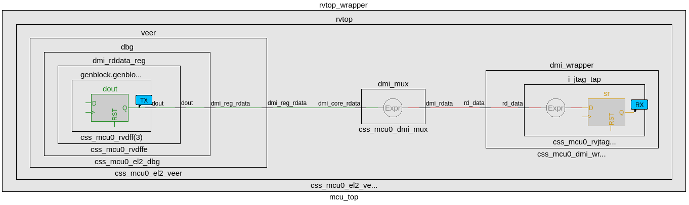
CDC analysis conclusions
- Missing synchronizers appear to be the result of “inferred” and/or only 2-FF instantiated synchronizers.
- dmi_jtag_to_core_sync.v contains inferred 2FF synchronizers on the control signals “dmi_reg_wr_en” and “dmi_reg_rd_en”.
- 2FF synchronizer inferences are considered non-compliant and should be replaced by an explicitly instantiated synchronization module, which is intended to be substituted on a per-integrator basis.
- cdc report scheme two_dff -severity violation
- Multi-bit signals are effectively pseudo-static and are qualified by synchronized control qualifiers.
- Pseudo-static: wr_data, wr_addr
- cdc signal reg_wr_data -module dmi_wrapper -stable
- cdc signal reg_wr_addr -module dmi_wrapper -stable
- Pseudo-static: wr_data, wr_addr
- The core clock frequency must be at least twice the TCK clock frequency of each TAP EPs for the JTAG data to pass correctly through the synchronizers.
CDC constraints
- cdc report scheme two_dff -severity violation
- cdc signal reg_wr_data -module dmi_wrapper -stable
- cdc signal reg_wr_addr -module dmi_wrapper -stable
- cdc signal rd_data -module dmi_wrapper -stable
- cdc signal reg_wr_data -module css_mcu0_dmi_wrapper -stable
- cdc signal reg_wr_addr -module css_mcu0_dmi_wrapper -stable
- cdc signal rd_data -module css_mcu0_dmi_wrapper -stable
- cdc signal jtag_dmi_req_i -module dmi_cdc -stable
- cdc signal jtag_dmi_resp_o -module dmi_cdc -stable
- cdc signal core_dmi_req_o -module dmi_cdc -stable
- cdc signal core_dmi_resp_i -module dmi_cdc -stable
Reset Domain Crossing
Reset Architecture
The below diagram illustrates the internal reset architecture of Caliptra SS.
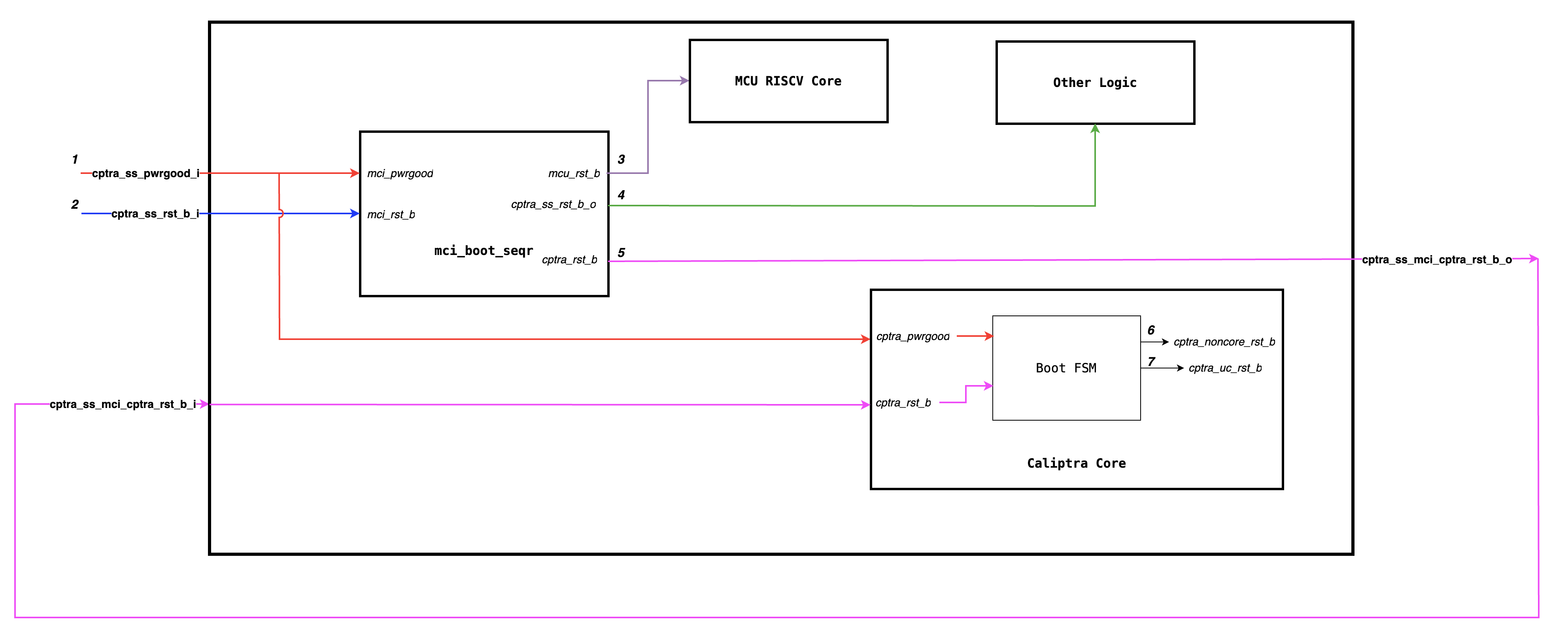
The reset block diagram below illustrates the RTL implemenation of various resets.
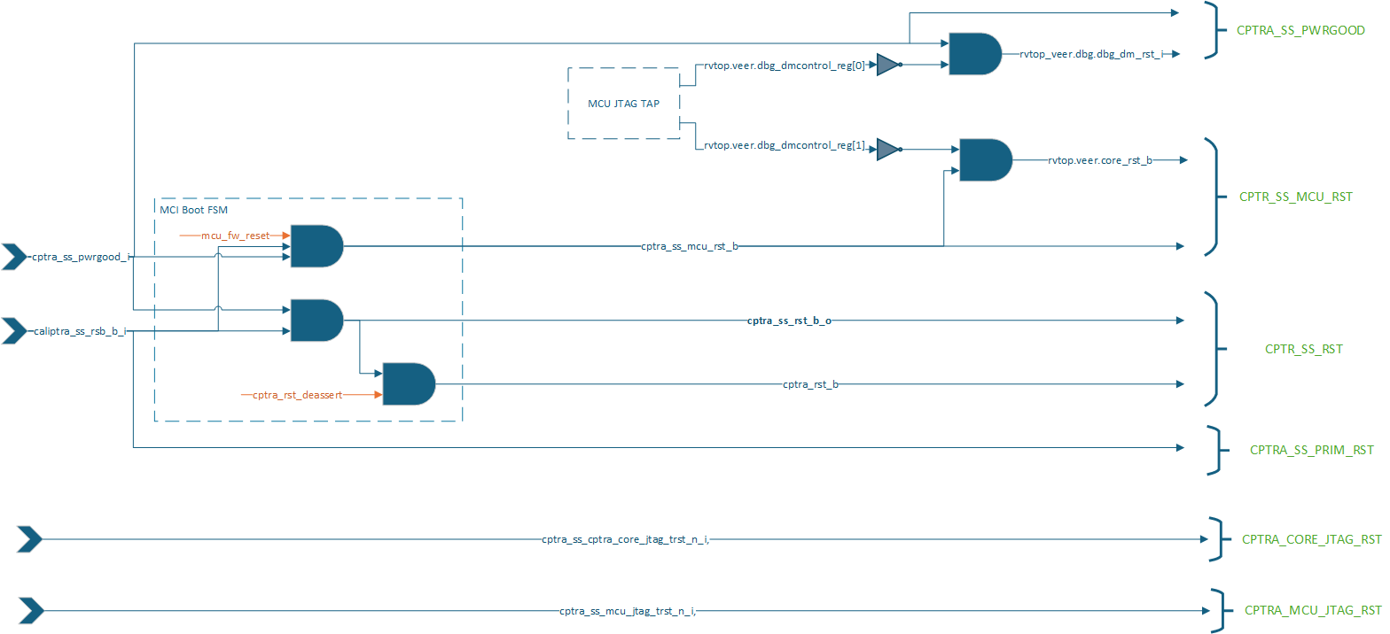
The below diagram illustrates how various internal blocks are connected to either primary resets or internally generated resets.
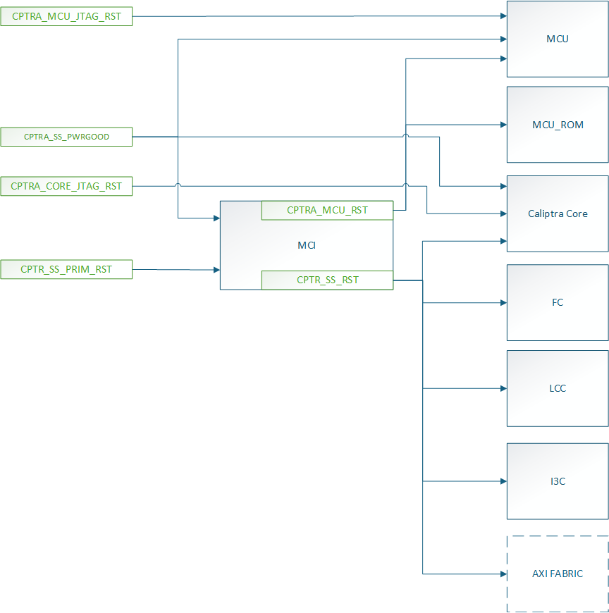
Similar to Caliptra Core, we solve the problem of RDC using gated clocks which are gated during reset assertion. Below diagram illustrates the clock connections of various sub-modules.
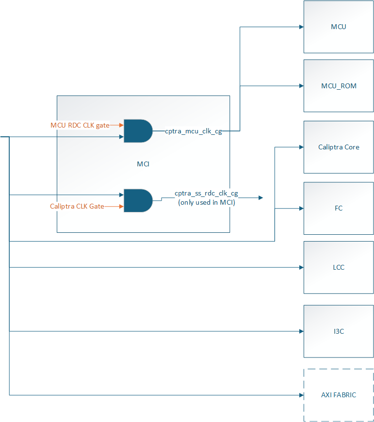
Reset Domain Stamping and Constraints
The Below table illustrates various reset domains that we have in the design. We assume that all resets are asserted at timestamp 5, and the constrained signal is held high or low around that time (for instance, from timestamp 2 to timestamp 8).
| Reset Group | Description | HW Reset Signal | Constraints | False path groups |
|---|---|---|---|---|
| CPTRA_SS_PWRGD | Primary reset input corresponding to SOC Powergood | cptra_ss_pwrgood_i | CPTRA_SS_PWRGD -> all | |
| CPTRA_SS_PRIM_RST | Primary reset input corresponding to SOC Warm Reset | cptra_ss_rst_b_i | caliptra_top_dut.soc_ifc_top1.soc_ifc_reg_hwif_out.CPTRA_FUSE_WR_DONE.done.value -> HIGH i3c.i3c.xrecovery_handler.xrecovery_executor.image_activated_o -> LOW i3c.i3c.xrecovery_handler.xrecovery_executor.payload_available_q -> LOW | CPTRA_SS_PRIM_RST -> CPTRA_CORE_UC_RST CPTRA_SS_PRIM_RST -> CPTRA_CORE_NON_CORE_RST CPTRA_SS_PRIM_RST -> CPTRA_SS_RST CPTRA_SS_PRIM_RST -> CPTRA_SS_MCU_RST |
| CPTRA_SS_RST | Caliptra SS MCI Boot Sequencer generated reset used by various other SS level logic blocks and Caliptra Core | cptra_ss_mci_cptra_rst_b_i mci_top_i.i_boot_seqr.cptra_ss_rst_b_o | mci_top_i.i_boot_seqr.rdc_clk_dis -> HIGH mci_top_i.i_boot_seqr.early_warm_reset_warn -> HIGH mci_top_i.i_boot_seqr.boot_fsm[3:0] = BOOT_IDLE i3c.i3c.xrecovery_handler.xrecovery_executor.image_activated_o -> LOW i3c.i3c.xrecovery_handler.xrecovery_executor.payload_available_q -> LOW caliptra_top_dut.soc_ifc_top1.soc_ifc_reg_hwif_out.CPTRA_FUSE_WR_DONE.done.value -> HIGH | CPTRA_SS_RST -> CPTRA_SS_PRIM_RST CPTRA_SS_RST -> CPTRA_CORE_NON_CORE_RST CPTRA_SS_RST -> CPTRA_CORE_UC_RST CPTRA_SS_RST -> CPTRA_SS_MCU_RST CPTRA_SS_RST -> CPTRA_DMI_NON_CORE_RST |
| CPTRA_CORE_NON_CORE_RST | Caliptra Core Boot FSM generated reset used by various other Caliptra Core logics | caliptra_top_dut.soc_ifc_top1.i_soc_ifc_boot_fsm.cptra_noncore_rst_b | caliptra_top_dut.soc_ifc_top1.i_soc_ifc_boot_fsm.rdc_clk_dis -> HIGH caliptra_top_dut.soc_ifc_top1.i_soc_ifc_boot_fsm.arc_IDLE -> HIGH mci_top_i.i_boot_seqr.rdc_clk_dis -> HIGH | CPTRA_CORE_NON_CORE_RST -> CPTRA_SS_RST CPTRA_CORE_NON_CORE_RST -> CPTRA_SS_PRIM_RST CPTRA_CORE_NON_CORE_RST -> CPTRA_CORE_UC_RST CPTRA_CORE_NON_CORE_RST -> CPTRA_SS_MCU_RST |
| CPTRA_CORE_UC_RST | Caliptra Core Boot FSM generated microcontroller reset for Caliptra Core RISCV | caliptra_top_dut.soc_ifc_top1.i_soc_ifc_boot_fsm.cptra_uc_rst_b | caliptra_top_dut.soc_ifc_top1.i_soc_ifc_boot_fsm.fw_update_rst_window -> HIGH caliptra_top_dut.aes_inst.aes_inst.u_aes_core.u_aes_control.gen_fsm[0].gen_fsm_p.u_aes_control_fsm_i.u_aes_control_fsm.aes_ctrl_cs[5:0] -> 6'b001001 | |
| CPTRA_SS_MCU_RST | Caliptra SS MCI Boot Sequencer generated microcontroller reset for Caliptra SS RISCV | mci_top_i.i_boot_seqr.mcu_rst_b | mci_top_i.i_boot_seqr.fw_update_rst_window -> HIGH mci_top_i.i_mci_mcu_trace_buffer.mcu_trace_rv_i_valid_ip -> LOW |
The current analysis only focuses on RDC crossing which are internal to Caliptra SS. Any RDC crossings with external flops need to be handled by integrators.
Reset Sequencing
The below waveform illustrates how various resets of Caliptra SS and Caliptra Core are sequenced in the design.
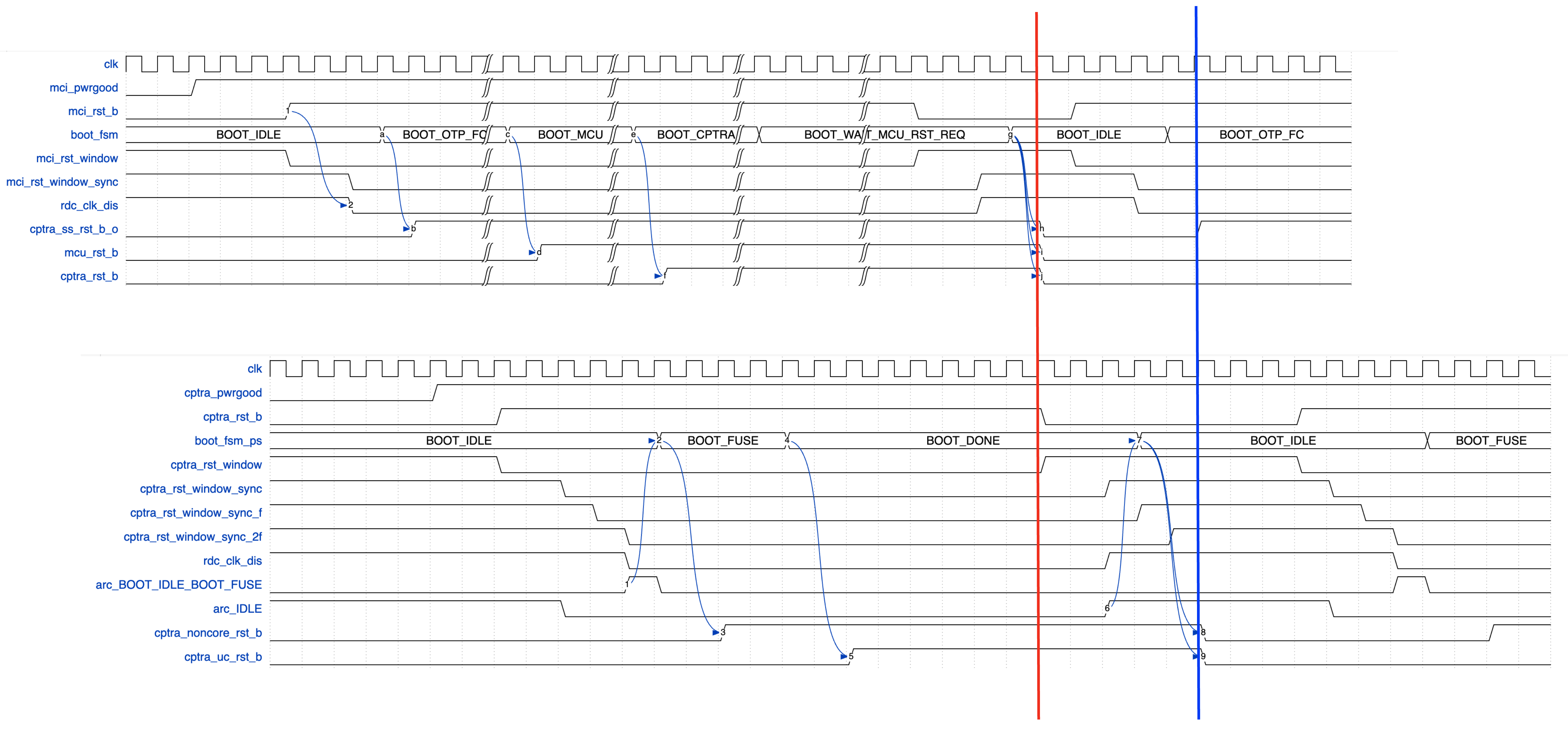
The red and blue line indicates that the input Caliptra SS warm reset (cptra_ss_rst_b_i) needs to be asserted for atleast 32 clock cycles for the reset assertion to propagate through various levels of hierarhcy.
RDC Waivers
All Caliptra Core waivers are applicable at SS level as well. On top of those, we have the following waivers.
create_view_criteria \
    -name otp_broadcast_ss_rst_caliptra_core \
    -rule {E_RST_METASTABILITY} \
    -comment "waiver_for otp_broadcast related paths" \
    -criteria { ((ResetFlop =~ "*.u_caliptra_ss.u_otp_ctrl.otp_broadcast_o.secret_prod_partition_0_data.*")  ||  \
                 (ResetFlop =~ "*.u_caliptra_ss.u_otp_ctrl.otp_broadcast_o.valid*") ) &&  \
                 ((MetaStableFlop =~ "*.u_caliptra_ss.caliptra_top_dut.soc_ifc_top1.i_soc_ifc_reg.field_storage.fuse_field_entropy*") || \
                  (MetaStableFlop =~ "*.u_caliptra_ss.caliptra_top_dut.soc_ifc_top1.i_soc_ifc_reg.field_storage.fuse_uds_seed*") ) } \
    -replace
set_rule_status -use_view_criteria otp_broadcast_ss_rst_caliptra_core -status Waived -weakmatchfullgroup

create_view_criteria \
    -name path_ending_at_2ff_sync \
    -rule {E_RST_METASTABILITY} \
    -comment "wavier for 2ff sync" \
    -criteria { ((MetaStableFlop =~ "*.u_sync_1.gen_generic.u_impl_generic.*") || \
                  (MetaStableFlop =~ "*.i_rst_window_sync.*") ) } \
    -replace
set_rule_status -use_view_criteria path_ending_at_2ff_sync -status Waived -weakmatchfullgroup

create_view_criteria \
    -name no_axi_bus_active \
    -rule {E_RDC_METASTABILITY} \
    -comment "Before warm reset assertion, it is sure that is transaction pending on axi bus" \
    -criteria {  (ResetFlop      =~ "*.caliptra_top_dut.s_axi_active[2:0]") && \
                 (MetaStableFlop =~ "*cg.user_soc_ifc_icg.clk_slcg_0_generated_icg.p_clkgate.vudpi0.q")  } \
    -replace
set_rule_status -use_view_criteria no_axi_bus_active -status Waived -weakmatchfullgroup
Synthesis
Synthesis has been performed at CALIPTRA_SS_WRAPPER level which encompasses the following :-
- caliptra_ss_top
- Memories instantiated outside using tech specific macros
Design converges at 400MHz 0.72V using an industry standard, advanced technology node as of 2025 April.
Recommended LINT rules
A standardized set of lint rules is used to sign off on each release. The lint policy may be provided directly to integrators upon request to ensure lint is clean in the SoC.
Known Lint Issue
The following lint violations are known and expected in the current implementation:
Signal Width Mismatches
| Location | Description | Justification |
|---|---|---|
| mcu_mbox_csr.sv:271 | Signal width mismatch | MSB on RHS will be optimized out during synthesis |
Undriven signals
These are undriven signals and deemed to be OK. If exposed to SOC leave unconnected when integrating.
| Location | Signal | Justification |
|---|---|---|
el2_veer.sv | sb_axi_bready_ahb | Caliptra Core internal RV processor uses AHB, not AXI interface, so AXI is unconnected |
el2_veer.sv | ifu_axi_bready_ahb | Caliptra Core internal RV processor uses AHB, not AXI interface, so AXI is unconnected |
el2_veer.sv | lsu_axi_bready_ahb | Caliptra Core internal RV processor uses AHB, not AXI interface, so AXI is unconnected |
Terminology
| Abbreviation | Term | Description |
|---|---|---|
| AXI | Advanced eXtensible Interface | A high-performance, high-frequency communication protocol |
| I3C | Improved Inter-Integrated Circuit | A communication protocol for connecting sensors and other peripherals. |
| ECC | Error Correction Code | A method of detecting and correcting errors in data storage and transmission. |
| RISCV | Reduced Instruction Set Computer Five | An open standard instruction set architecture based on established RISC principles. |
| MCU | Manufacturer Control Unit | A small computer on a single integrated circuit containing a processor core, memory, and programmable input/output peripherals. |
| MCI | Manufacturer Control Interface (for MCU) | Manages the communication between the processor and the memory components. |
| FC | Fuse Controller | A one-time programmable memory controller used for storing critical configuration data and security keys. |
| LCC | Life Cycle Controller | Manages the different stages of the subsystem's lifecycle, including initialization, operation, and shutdown. |