8fed18c
![]()
Caliptra: A Datacenter System on a Chip (SoC) Root of Trust (RoT)
Revision 1.0
Version 1.0
Introduction
Caliptra1 was originally created as part of the Open Compute Project (OCP). The major revisions of the Caliptra specifications are published at OCP. The evolving source code and documentation for Caliptra are in this repository within the CHIPS Alliance Project, a Series of LF Projects, LLC.
The objective of Caliptra is to define core RoT capabilities that must be implemented in the System on Chip (SoC) or ASIC of any device in a cloud platform. The collection of these RoT capabilities is referred to as the Silicon RoT Services (Silicon RoT).
Background
The overall security posture of silicon devices depends on establishing a core root of trust (RoT) and chain of trust. The core root of trust and chain of trust must attest to the integrity of configuration and mutable code.
Traditional RoT architectures offer many intrinsic security services and hosted security applications on a trusted execution environment (TEE). These architectures include (but are not limited to) hardware capabilities (cryptographic and microprocessor), ROM, firmware, and API infrastructure. These solutions are instantiated in discrete or integrated forms in various platform and component architectures.
Some of these solutions are either proprietary or aligned to specific parts of industry standards, consortium, or association specifications; for example, National Institutes of Standards and Technology (NIST), Open Compute Project (OCP), Trusted Computing Group (TCG), Distributed Management Task Force (DMTF), Institute of Electrical and Electronics Engineers (IEEE), etc. These solutions may be certified to conform to various standards; for example, the NIST cryptographic algorithm Validation program (CAVP).
Establishing a consistent RoT on very different hardware configurations while maintaining configuration and deployment flexibility is challenging. There is no uniform configuration across Cloud Service Providers (CSPs). For example, a system with host processors has very different firmware security measures when compared to a system without head-nodes or host processors.
The OCP Security WG specifications are making progress toward establishing the platform and peripheral security architecture recommendations that are necessary to attain the desired consistency in platform security orchestration.
Silicon RoT goals
To drive agility of specification definition and to maximize applicability, the scope of Caliptra is deliberately minimalistic. This minimalist approach drives industry alignment, consistency, and faster adoption of foundational device security primitives. A well and narrowly defined specification maximizes architectural composability; reusability across CSPs, products, and vendors; and feasibility of open sourcing.
Enhancements and advanced use cases and applications are outside the scope of this specification and may be developed in the form of a roadmap for the Silicon RoT and community engagement.
Caliptra defines a design standard for a Silicon internal RoT baseline. This standard satisfies a Root of Trust for Measurement (RTM) role. The open-source implementation of Caliptra drives transparency into the RTM and measurement mechanism that anchor hardware attestation. The SoC must measure the code and configuration it boots into Caliptra. Caliptra must store these measurements and report them with signed attestations rooted in unique per-asset cryptographic entropy. As such, Caliptra serves as a Root of Trust for Identity (RTI) for the SoC.
To satisfy these Silicon RoT goals, no other capabilities are part of this specification. This scope decouples platform integrity capabilities that can be enforced and evolve independently through other platform devices or services – such as update, protection, and recovery.
Within this scope, the goals for a Caliptra 1.0 specification include:
- Definition and design of the standard silicon internal RoT baseline:
- Reference functional specification:
- Scope including RTM and RTI capabilities
- Control over SoC non-volatile state, including per asset entropy
- Reference APIs:
- Attestation APIs
- Internal SoC services
- Reference implementation
- Open source reference (including RTL and firmware reference code):
- For implementation consistency, using open source dynamics to avoid pitfalls and common mistakes
- For accelerated adoption, so that future products can leverage existing designs and avoid having to start the design process from scratch
- For greater transparency, to avoid fragmentation in the implementation space
- Firmware and RTL logical design are open, managed by consortium
- Reference functional specification:
- Consistency - across the industry in the internal RoT (iRoT) architecture and implementation:
- DICE identity, measurement, and recovery
- The silicon iRoT scope includes all datacenter-focused server class SoC / ASIC (datacenter focused) devices (SSD - DC, NIC, CPU, GPU - DC):
- Critical priority are devices with the ability to handle user plain text data
- Top priority are CPU SoCs
- Other examples include SmartNIC and accelerators
- Over time, the scope includes further datacenter devices
- SSD, HDD, BMC, DIMM
- Critical priority are devices with the ability to handle user plain text data
Note that Caliptra reference code (including RTL and firmware) is intended to be adopted as-is, without modification.
Explicitly out of scope is how silicon integration into backend work is performed such as:
- Foundry IP integration
- Physical design countermeasures
- Analog IPs
- Post manufacture test and initialization (OSAT)
- Certification
Use cases
The Silicon RoT use cases can be supported through the adoption of specific industry standards, and association and consortium specifications. For more information, see specific documents in References.
In this version of the specification, the desired capabilities address the basics of supply chain security use cases.
Supply chain security
- Mutable code integrity: The objective is to prove the device is running genuine firmware such that the device manufacturer can vouch for its authenticity and integrity, and the device owner can ensure only authorized updates are applied to the device. This flow is aligned with Reference 9 and can be achieved with dual signature verification of equal imposition.
- Configuration and lifecycle management: The objective is to allow the platform owner to securely configure the RoT capabilities, and to enable and authorize lifecycle state transitions of the SoC.
DICE Protection Environment
Caliptra implements the DICE Protection Environment (DPE) API, allowing it to derive and wield a DICE identity on behalf of other elements within the SoC. Use cases for this API include serving as a signing oracle for a Security Protocol and Data Model (SPDM) responder that is executing in the SoC application processor, as well as authentication to a discrete TPM device.
Industry standards and specifications
This specification follows the industry standards and specifications listed in References.
NIST SP 800-193 Platform Firmware Resiliency
Per Reference 1, RoT subsystems are required to fulfill three principles: protection, detection and recovery. The associated RoT services are referred to as:
- The Root of Trust for Update (RTU) is responsible for authenticating firmware updates and critical data changes to support platform protection capabilities.
- The Root of Trust for Detection (RTD) is responsible for firmware and critical data corruption detection capabilities.
- The Root of Trust for Recovery (RTRec) is responsible for recovery of firmware and critical data when corruption is detected, or when instructed by an administrator.
These RoT services can be hosted by a complex RoT as a whole or these services can be spread across one or more components within a platform. This determination has a basis in physical risk. Physical adversaries with reasonable skill can bypass a discrete RoT’s detection capabilities, for example, with SPI interposers.
However, an RoT embedded within a SoC or ASIC represents a much higher detection bar for a physical adversary to defeat. For this reason, Caliptra shall deliver the Detection capability for itself while providing Measurement and Identity services for the rest of the SoC. The Measurement and Identity services that Caliptra provides can be used by the SoC to create Detection capability for the measured firmware and configuration data.
With the objectives of minimalistic scope for Silicon RoT and maximizing applicability and adoption of this specification, Update and Recovery are decoupled from Caliptra and are expected to be provided by an external RoT subsystem, such as a discrete RoT board element on a datacenter platform. Because a physical adversary can trivially nullify any recovery or update capabilities, no matter where implemented, decoupling represents no regression in a security posture, while enabling simplicity and applicability for the internal SoC silicon RoT.
Detection of corrupted critical code and data (configuration) requires strong end to end cryptographic integrity verification. To meet the RTD requirements, Silicon RoT shall:
- Cryptographically measure its code and configuration
- Sign these measurements with a unique attestation key
- Report measurements to a host or external entity, which can further verify the authenticity and integrity of the device (also known as attestation)
Measurements include Code and Configuration. Configuration includes invasive capabilities that impact the user service level agreement (SLA) on confidentiality; for example, the enablement of debug capabilities that grant an operator access to raw, unencrypted registers for any tenant context. In order to measure and attest configuration, the Silicon RoT must be in control of the configuration.
As an extension to controlling configuration, the Silicon RoT must control the security states (for more information, see Caliptra Security States). Certain security states by design grant full invasive capabilities to an external operator, for debug or field analysis.
Measurements must be uniquely bound to the device and its manufacturer at a minimum. This establishes the need for Identity services in the Silicon RoT, which serve as the basis for key derivation and attestation authenticity.
For further details about how Caliptra addresses NIST SP 800-193, see Device Resilience.
Trusted Computing Group (TCG) DICE Attestation
In accordance with OCP Attestation specification Reference 8, devices must have a cryptographic identity for the endorsement of attestation quotes. The RTM implementation follows TCG DICE (for information, see Reference 4, Reference 5, and Reference 6). One of the benefits of TCG DICE device identities is having renewable security. This renewability complements ownership transfer and circular economy. The new owner is not burdened with the identity of the previous owner, nor is the new owner burdened with trusting an irrevocable hardware identity certificate. This benefits the transferee, as their identities can be revoked through standard PKI mechanisms. DICE based certificates are fully compatible with Public Key Infrastructure (PKI), including full lifecycle management and PKI Certificate Revocation List (CRL).
Operational security during the manufacturing process is critical, to ensure the DICE entropy is securely initialized, certified, and registered. Operational security avoids any pilfering of this asset by eavesdroppers. Operational security is outside the scope of this specification.
Threat model
The Caliptra threat model describes attacker profiles, assets and attack surfaces, and paths to these assets based on attacker profiles. Subsections provide further details.
Threat scenarios as comprehended by assets and possible attack paths are as complete as possible but focus on the worst case scenarios. Thus not every attack path to asset is captured in this threat model.
Attacker profiles
An attacker profile is based on factors like the tools that are accessible to the attacker, the level of access to the target of evaluation, and expertise of the attacker to use these methods. These factors are described in the following tables.
Table 1: Tools accessible to attacker
| Attack tools | Type of attack | Purpose and usage |
|---|---|---|
| Debuggers, fuzzing devices, image reverse engineering tools, and software payloads | Logical fault injection | Find logical and functional vulnerabilities and exploit those to achieve unauthorized operations. |
| Clock fault injectors, voltage fault injectors, electromagnetic fault injectors, optical fault injectors, and micro probing | Environmental fault injection | Alter the execution flow of the critical decision points, especially in the early execution. |
| Power analyzers, timing analyzers (scopes, etc.), low speed bus analyzers, and optical emission analyzers | Side channel analysis | Infer security sensitive information by analyzing various operational conditions. |
| Microscopic imaging, reverse engineering, scanning electron microscope imaging, and focused ion beam (FIB) | Chip invasive attacks | Decapsulation, depackaging, and rebonding to probe the internals of the chip. |
Table 2: Type of access to level of access
| Type of access | Levels of access | Attack paths available |
|---|---|---|
| Physical access | Unrestricted access for physical and logical attacks. | Chip invasive attacks and chip non-invasive attacks |
| Remote access | Limited access for attacks with both privileged and unprivileged access rights. | Chip non-invasive attacks and network attacks |
Table 3: Definition of expertise (JIL)
| Proficiency level | Definition | Detailed definition |
|---|---|---|
| Expert | Can use chip invasive, fault injections, side channels, and logical tools. Understands hardware and software in depth. Familiar with implementation: - Algorithms - Protocols - Hardware structures - Principle and security concepts | Developer-level knowledge of algorithms, protocols, hardware structure, and principles. Understands techniques and tools for attacks. |
| Proficient | Can use fault injections, side channels, and logical tools. Has reasonable understanding of hardware and software. Familiar with security behavior. | Familiar with security behavior and classical attacks. |
| Layperson | No particular expertise. | No particular expertise. |
Types of attacks
Physical attacks
A physical attacker has full access to the electrical and physical components. This includes access to interfaces, connectors, and ports of the SoC/ASIC in which Caliptra is integrated without restriction.
Invasive attacks that involve depackaging or delayering of the SoC/ASIC are out-of-scope. Non-invasive attacks are in scope.
- Fault injection attacks
- Counter measurements - as strong recommendation
- Power and electromagnetic analysis attacks
- Counter measurements - as strong recommendation
Table 4: Attack types
| Attack | Description | Threat model scope |
|---|---|---|
| Electromagnetic – passive | Attacker observes the electromagnetic power spectrum and signals radiated from the product. | - Includes all attacks at all frequency ranges, including radio frequencies, infrared, optical, and ultraviolet. - Excludes attacks that require removing the package lid. |
| Electromagnetic – active | Attacker directs electromagnetic radiation at the product or portions of the product. | - Includes all attacks at all frequency ranges, including radio frequencies, infrared, optical, and ultraviolet. - Excludes attacks that require removing the package lid. |
| Electric – passive | Attacker probes the external pins of the package and observes electrical signals and characteristics including capacitance, current, and voltage signal. | - Includes both analog attacks and digital signal attacks. - Excludes attacks that require removing the package lid. |
| Electric – active | Attacker alters the electrical signal or characteristics of external pins. | - Includes both analog attacks and digital signal attacks. - Excludes attacks that require removing the package lid. |
| Temperature – passive | Attacker observes the temperature of the product or portions of the product. | Excludes attacks that require removing the package lid. |
| Temperature – active | Attacker applies external heat sources or sinks to alter the temperature of the product, possibly in a rapid fashion. | - Includes all temperature ranges (for example, pouring liquid nitrogen over the package or heating the package to above 100 C). - Excludes attacks that require removing the package lid. |
| Sound - passive | Attacker observes the sounds emitted by the product. | - Includes all frequencies. - Excludes attacks that require removing the package lid. |
Table 5: Logical attacks
| Attack | Description | Threat model scope |
|---|---|---|
| Debug and register interfaces | Manipulation of externally accessible registers of Caliptra. | Includes all buses that are accessible to components external to Caliptra, including JTAG. |
| Software interfaces | Attacker invokes software interfaces that are exposed by Caliptra to external components. | Includes all externally exposed software interfaces from both non-RoT firmware as well as interfaces accessed by external IP blocks. Includes exploiting both design and implementation flaws. For high value assets only (see next subsection), the attacker is assumed to fully control all mutable code of the SoC, including privileged Caliptra mutable code. |
| Side channel - timing | Attacker observes the elapsed time of different sensitive operations. | Includes attacks where the attacker actively stimulates the sensitive operations while timing. |
| Cryptographic analysis | Attacker observes plaintext, ciphertext, related data, or immediate values in cryptography to overcome cryptographic controls. | Includes all practical cryptanalysis attacks. Assumes NIST-unapproved algorithms provide no security (for example, SHA-1, Single DES, ChaCha20). Assumes any cryptographic algorithm that provides less than 128 bits of security (as determined by NIST SP 800-57) provides no security. Excludes quantum computer attacks. This exclusion will be removed soon. |
Trust boundaries
The following figure shows trust boundaries for the discussion of threat modeling. SoCs based on Caliptra are expected to have Caliptra as silicon RoT, and are expected to have a platform or SoC security engine to orchestrate SoC security needs for the rest of the SoC.
Trust levels of Caliptra and the SoC security engine are not hierarchical. These two entities are responsible for different security aspects of the chip.
Figure 1: Caliptra trust boundaries
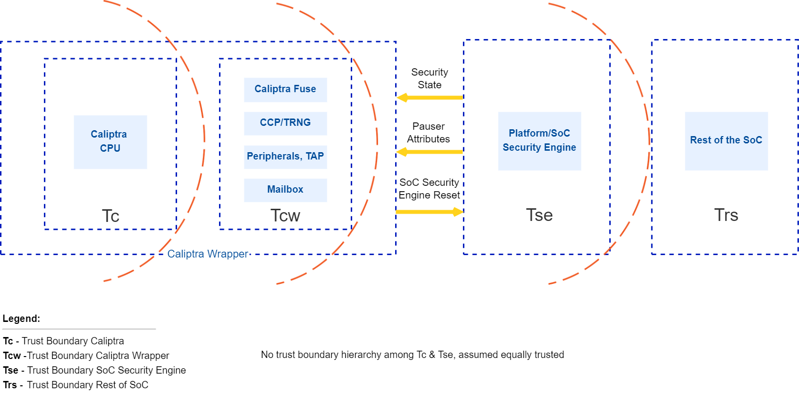
Caliptra interactions
The Caliptra Core blocks consume the Tc and Tcw trust level components. This boundary includes crypto accelerators, hardware key sequencer, key vault, Caliptra microcontroller, ROM, and subsystem interconnects. The Caliptra Core provides deterministic Caliptra behavior. Caliptra interacts with components in the Tse and Trs trust levels.
Caliptra assets and threats
Assets are defined to be secrets or abilities that must be protected by an owner or user of the asset. Ownership means that the owner has the responsibility to protect these assets and must only make them available based on a defined mechanism while protecting all other assets.
An example of when an owner must protect assets is moving from secure mode to insecure mode. Another example is moving from one owner to another. Before moving through these transitions, the owner must ensure all assets are removed, disabled, or protected based on how the use case is defined.
Table 6: Assets
| Asset category | Asset | Security property | Attack profile | Attack path | Mitigation |
|---|---|---|---|---|---|
| Fuse/OTP high value secrets | UDS Seed | Confidentiality and integrity | Expert | Malicious manufacturing spoofing of UDS Seeds | UDS obfuscation with class RTL key |
| Fuse/OTP high value secrets | UDS Seed | Confidentiality and integrity | Expert | Invasive attack (fuse analysis) | Shield fuse IP |
| Fuse/OTP high value secrets | UDS Seed | Confidentiality and integrity | Expert | Boot path tampering while retrieving UDS values | UDS obfuscation with class RTL key |
| Fuse/OTP high value secrets | UDS Seed | Confidentiality and integrity | Expert | Attempting to derive die specific keys by knowing UDS | Confine unobfuscated UDS and subsequent derivations to key vault |
| Fuse/OTP high value secrets | Field entropy | Confidentiality and integrity | Expert | Malicious manufacturing spoofing on field entropy | Field entropy obfuscation with class RTL key |
| Fuse/OTP high value secrets | Field entropy | Confidentiality and integrity | Expert | Invasive attack (fuse analysis) | Shield fuse IP |
| Fuse/OTP high value secrets | Field entropy | Confidentiality and integrity | Expert | Boot path tampering while retrieving field entropy values | Field entropy obfuscation with class RTL key |
| Fuse/OTP high value secrets | Field entropy | Confidentiality and integrity | Expert | Attempting to derive die specific keys by knowing field entropy | Confine unobfuscated field entropy and subsequent derivations to key vault |
| Fuse/OTP high value secrets | FW authentication keys | Integrity | Proficient | Glitching | 1. Redundant decision making on critical code execution 2. Error check before consuming values from fuses 3. Environmental monitoring and protection |
| Fuse/OTP high value secrets | Versioning information from fuses | Integrity | Proficient | Glitching | Environmental monitoring and protection |
| Fuse/OTP high value secrets | IDEVID CERT chain | Integrity | Proficient | Glitching | 1. Environmental monitoring and protection 2. Error check before consuming values from fuse in various ways |
| Die unique assets | UDS (802.1AR Unique Device Secret) | Confidentiality and integrity | Proficient | 1. Software reading actual secrets 2. Side channel attack to infer secret | 1. Secrets locked in key vault, not readable by software 2. SCA protections |
| Die unique assets | CDIn (DICE compound device identifier for Layer n) | Confidentiality and integrity | Proficient | 1. Software reading actual secrets 2. Side channel attack to infer secret | 1. Secrets locked in key vault, not readable by software 2. SCA protections |
| Die unique assets | IDevIDPriv | Confidentiality and integrity | Proficient | 1. Software reading actual secrets 2. Side channel attack to infer secret | 1. Secrets locked in key vault, not readable by software 2. SCA protections |
| Die unique assets | LDevIDPriv | Confidentiality and integrity | Proficient | 1. Software reading actual secrets 2. Side channel attack to infer secret | 1. Secrets locked in key vault, not readable by software 2. SCA protections |
| Die unique assets | Obfuscation key | Confidentiality and integrity | Proficient | 1. Software reading actual secrets 2. Side channel attack to infer secret | 1. Secrets locked in key vault, not readable by software 2. SCA protections |
| Die unique assets | AliasFMC_KeyPriv | Confidentiality and integrity | Proficient | 1. Software reading actual secrets 2. Side channel attack to infer secret | 1. Secrets locked in key vault, not readable by software 2. SCA protections |
| Die unique assets | AliasRT_KeyPriv | Confidentiality and integrity | Proficient | 1. Software reading actual secrets 2. Side channel attack to infer secret | 1. Secrets locked in key vault, not readable by software 2. SCA protections |
| Root of trust execution | ROM FW | Integrity | Proficient | Glitching | 1. Redundant decision making on critical code execution 2. Environmental monitoring and protection |
| Root of trust execution | Execution unauthorized runtime FW | Authenticity and integrity | Proficient | Modify boot media | Authenticity and integrity check using PKI DSA upon power on |
| Root of trust execution | Execution unauthorized runtime FW | Authenticity and integrity | Proficient | Arbitrary payload pushed into execution | Authenticity and integrity check using PKI DSA during software updates and power on |
| Root of trust execution | Rollback Attack | Versioning | Proficient | 1. Modify boot media to host older versions 2. Bypass version check during boot | 1. Authenticity and integrity check using PKI DSA upon power on 2. Failproof, audited boot code implementation responsible for loading images |
| Root of trust execution | Control flow | Integrity and confidentiality if applicable | Proficient | 1. Return and jump addresses manipulation 2. Return values and errors tampering 3. Stack overflow 4. Buffer overflows 5. Privilege escalations and hijacking | 1. Various control flow integrity measures 2. Secure coding practices and auditing implementation |
| Boot measurements protected by Caliptra | Boot measurements that Caliptra gathers, stores, and reports | Integrity | Expert | 1. Manipulate measurements AiTM while in transit to Caliptra 2. SoC sends manipulated measurements to Caliptra | |
| Caliptra inputs | Security state | Integrity | Proficient | Glitching | Environmental monitoring and protection |
| Caliptra inputs | Mode selection (Boot Media Integrated and dependent selections) | Integrity | Proficient | Glitching | Environmental monitoring and protection |
| Caliptra inputs | PAUSER attribute | Integrity | Proficient | Glitching | Environmental monitoring and protection |
| Caliptra inputs | Design-for-Test (DFT) and Design-for-Debug (DFD) | Integrity | Proficient | 1. Attempt to manipulate RoT execution via DFT or DFD flows to flows that are not plan-of-record 2. Attempt to retrieve device secrets via DFT or DFD flows when product is field-deployed 3. Attempt to retrieve device secrets via DFT or DFD flows while the product is being developed and debugged | Implement scan mode and debug unlock management within Caliptra with the required SoC support |
High level architecture
The following figure shows the basic high-level blocks of Caliptra.
Figure 2: Caliptra high level blocks
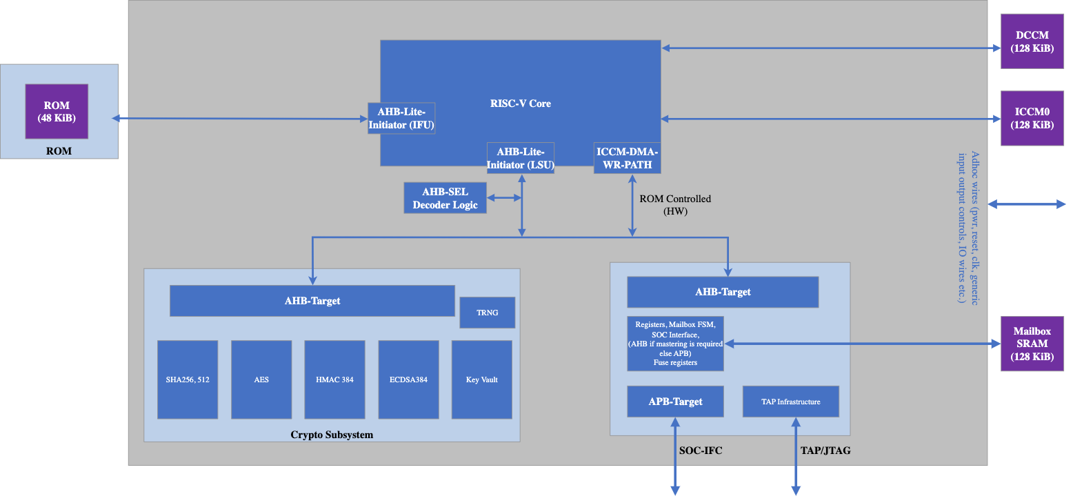
See the hardware section for a detailed discussion.
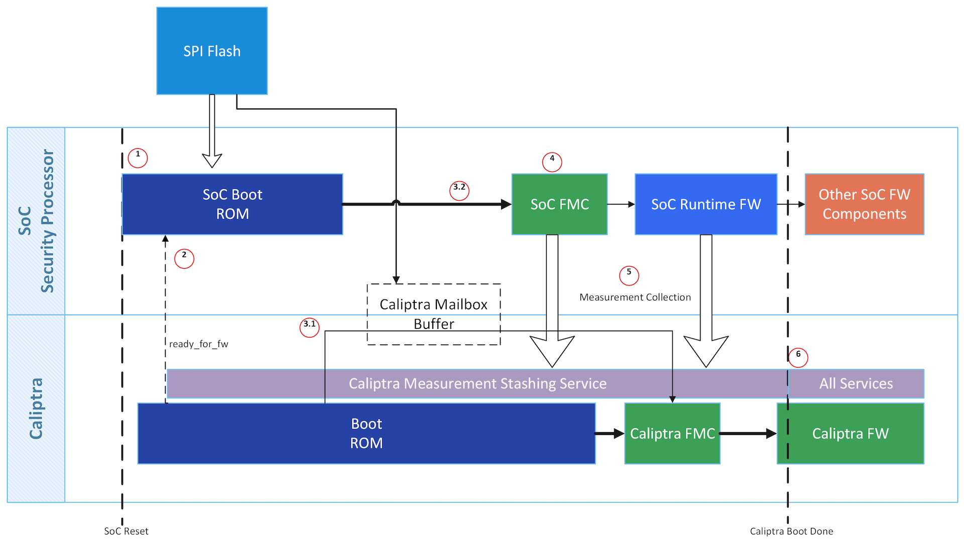
Caliptra is among the first uncore microcontrollers taken out of reset by the power-on reset logic. Caliptra coordinates the start of the firmware chain-of-trust with the immutable component of the SoC ROM. After the Caliptra ROM completes initialization, it provides a "stash measurement" API and callback signals for the SoC ROM to proceed with the boot process. Caliptra ROM supports stashing of at most eight measurements prior to the boot of Caliptra firmware. The SoC then may choose to boot Caliptra firmware. Any security-sensitive code or configuration loaded by the SoC prior to Caliptra firmware boot must be stashed within Caliptra. If the SoC exceeds Caliptra ROM's measurement stash capacity, attestation must be disabled until the next cold reset. The boot process is as follows:
- Hardware executes SoC power-on reset logic. This logic starts the execution of SoC ROM and Caliptra ROM.
- SoC ROM waits for the ready_for_fw signal from Caliptra ROM.
- SoC ROM fetches the FMC.
- If the FMC is Caliptra firmware:
- SoC ROM loads the Caliptra firmware into the Caliptra mailbox and issues the Caliptra "firmware load" command.
- Caliptra ROM authenticates, measures, and starts the Caliptra firmware.
- If the FMC is not Caliptra firmware:
- SoC ROM measures that firmware as the SoC FMC, and issues the Caliptra "stash measurement" command prior to executing SoC FMC.
- If the FMC is Caliptra firmware:
- SoC ROM executes SoC FMC.
- SoC FMC continues the boot process, forming a boot firmware chain-of-trust: each firmware fetches, authenticates, measures, and executes the next firmware needed to establish the device operating environment. Each firmware deposits the next firmware's measurements into Caliptra prior to execution. The exception is Caliptra's firmware: SoC firmware delegates the measurement and execution of Caliptra's firmware to Caliptra ROM.
- Upon eventual initialization, Caliptra firmware presents attestation APIs using the deposited measurements.
See Error Reporting and Handling for details about Caliptra and SoC firmware load and verification error handling.
Figure 3: Caliptra boot flow
Identity
Caliptra must provide its runtime (RT) code with a cryptographic identity in accordance with the TCG DICE specification. This identity must be rooted in ROM, and provides an attestation over the security state of the RTM as well as the code that the RTM booted.
Figure 4: DICE Cert/Key generation
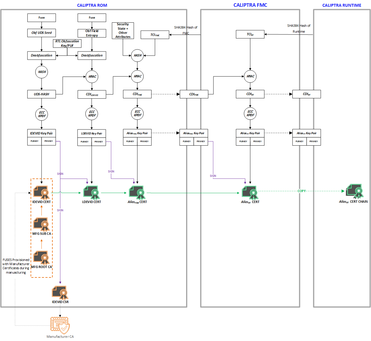
UDS
A combination of mask ROM and HW macros must implement the DICE key derivation and power-on latch, hiding the UDS seed and only making the CDI-derived signing public key visible to ROM and private key 'handle' available to ROM. Real UDS will only be calculated during the cold boot, used for CDI derivation and immediately gets cleared.
The Caliptra UDS seed is stored as ciphertext in fuses, deobfuscated only on cold boot using an obfuscation key2 known only to the Caliptra Hardware. Once read by Caliptra HW at boot, the unobfuscated UDS is then used to derive the IDevID identity and immediately cleared by hardware.
IDevID key
Caliptra's IDevID key is a hardware identity generated by Caliptra ROM during manufacturing. This key "handle" must be solely wielded by Caliptra ROM, and shall never be exposed externally at any phase of the Caliptra lifecycle. IDevID is used to endorse LDevID. The IDevID certificate is endorsed by the vendor’s provisioning CA (pCA) that is implemented via a HSM appliance connected to High Volume Manufacturing (HVM) flows (see provisioning CA in Reference 8).
See Provisioning IDevID During Manufacturing for further details on IDevID provisioning.
LDevID key
Caliptra shall support field-programmable entropy, which factors into the device's LDevID identity. The LDevID certificate is endorsed by IDevID and in turn endorses the FMC alias key.
Caliptra's field-programmable entropy shall consist of two 16-byte slots. All slots are used to derive LDevID. An owner may decide to program as few or as many slots as they wish. Upon programming new entropy, on the next reset the device begins wielding its fresh LDevID. Owners need to validate the new LDevID by using IDevID.
Commentary: threat analysis
An ideal IDevID has the following properties:
- Cannot be altered by entities besides Caliptra in manufacturing security state.
- Cannot be impersonated by entities that are not a Caliptra instatiation for that device class.
- Cannot be cloned to additional devices of the same class.
- Private component cannot be extracted from Caliptra.
Caliptra 1.0 alone does not fully address these properties. For example, a person-in-the-middle supply chain adversary could impersonate Caliptra by submitting its own IDevID Certificate Signing Request (CSR) to the pCA. Vendors should threat model the IDevID generation and endorsement flows for their SoC. Threat actors to consider are the following:
- Components involved in UDS injection flows: can they inject the same obfuscated UDS to multiple devices, or to devices of different classes? Can they wield the obfuscation key to leak the UDS?
- Components servicing the connectivity between the Caliptra instantiation and the HSM applicance performing IDevID endorsement: can they alter or impersonate Caliptra's IDevID CSR?
- Physical attackers: see Physical Attack Countermeasures.
Vendors have incentives to mitigate these threats. The vendor identity chain secures RMA and confidential computing workflows.
Ultimately though, IDevID is not renewable. Renewable security, often referred to as trusted computing base recovery, is a base design principle in Caliptra. Therefore, it is a design goal to reduce the operational dependency on IDevID. Field entropy and LDevID satisfy this need.
Field entropy is a limited resource, consisting of only two 16-byte slots of one-time programmable fuses. It is not generally expected that a second-hand purchaser can program all or even any of these slots. Caliptra's DICE identity remains usable even after all field entropy slots are programmed, so this feature does not preclude a circular economy. Field entropy is a feature primarily designed for users who purchase new parts.
Field entropy and LDevID are intended to hedge against attackers with the following abilities:
- Can obtain UDS before the part first arrives at the owner's facility.
- Can wield that stolen UDS to impersonate the part after it is deployed within the owner's facility. The attacker can derive and wield IDevID to mint an attacker-controlled DICE hierarchy; for example, LDevID, FMC alias key, or Runtime firmware alias key.
- Cannot fully impersonate the part during initial onboarding within the owner's facility.
- Cannot extract field entropy after initial onboarding.
During initial onboarding, the owner is expected to instruct the device to program field entropy. Upon device reset, this results in a fresh LDevID. Attackers that have previously obtained UDS are not able to derive this LDevID. The owner is expected to register the new LDevID and subsequently validate all future DICE keys for the device against that LDevID.
When registering LDevID during device onboarding, the owner is expected to rely on IDevID as an authenticity signal over LDevID. It is assumed that the attacker has obtained UDS at this point, and therefore can themselves wield IDevID. Therefore, the authenticity signal granted by IDevID cannot be the only signal used to determine LDevID's trustworthiness. The owner's device onboarding flow must be resistant to remote person-in-the-middle attackers that may attempt to use a previously exfiltrated UDS to register a forged LDevID.
After an owner registers a device's LDevID as part of their device onboarding flow, and unless the device again passes through the owner's device onboarding flow, the owner should not trust IDevID to endorse any other LDevIDs.
This approach does not defend against supply-chain attackers that obtain fuse data for devices that enter the supply chain after their field entropy has been programmed, such as during RMA flows. The LDevID certificate also does not support revocation because there is no generic Caliptra OCSP service. Owners should either maintain an allowlist of LDevID certificates or revoke any of the upstream certificate authorities.
Owners are not required to program field entropy. Caliptra generates LDevID from the value of the field entropy fuses, which could be all zeroes or ones. Caliptra LDevID derivation descends from UDS so that LDevID properties are no worse than IDevID. Field entropy is expected to be stored in fuses to achieve an equivalent physical attack barrier to UDS.
It is the responsibility of the owner or the user to identify the certificate they wish to trust, and to potentially endorse with their own certificate authority: pCA, IDevID, LDevID, or AliasFMC.
FMC alias key
The LDevID CDI is mixed with a hash of FMC, as well as the security state of the device, via a FIPS-compliant HMAC, to produce CDIFMC. ROM uses CDIFMC to derive the AliasFMC keypair. ROM wields LDevID to issue a certificate for Alias. The AliasFMC certificate includes measurements of the security state and FMC. ROM makes CDIFMC, AliasFMC, and its certificate, available to FMC.
FMC mixes CDIFMC with a hash of runtime firmware to produce CDIRT. FMC uses CDIRT to derive the AliasRT alias keypair. FMC wields AliasFMC to issue a certificate for AliasRT. This alias certificate includes measurements of runtime firmware. FMC makes CDIRT, AliasRT, and its certificate, available to application firmware, while withholding CDIFMC and AliasFMC.
Security state
Devices may support features like debug unlock, DFT, or DFD flows that globally affect SoC state. These features, when enabled, significantly alter the security state of the device. The configuration of these features shall be captured in the device's DICE identity. The security state shall be captured as an input to the FMC's CDI, and represented within the FMC's alias certificate.
Owner authorization
Caliptra firmware shall be signed by the vendor. In addition, this firmware may also be signed by the owner when ownership control is enforced. If a second signature is present for ownership authorization, Caliptra must extract the owner's public key from the firmware image during cold boot, and latch the owner key into Caliptra's RAM for the remainder of its uptime3. Caliptra then uses both the vendor key and owner key to verify hitless firmware updates.
Caliptra shall attest to the value of the owner key, enabling external verifiers to ensure that the correct owner key was provisioned into the device. To perform this attestation, Caliptra includes the owner key as an input to the FMC's CDI (as part of "other attributes" from Figure 4 above), and represents it within the FMC's alias certificate.
The SoC may support a fuse bank for representing the hash of the owner's public key. If the SoC reports this value to Caliptra, Caliptra refuses to boot firmware unless the firmware was dual-signed by the key reported by SoC ROM's fuse registers.
The owner key, when represented in fuses or in the FMC's alias certificate, is a SHA384 hash of a structure that contains a list of owner public keys. This supports key rotation.
Provisioning IDevID during manufacturing
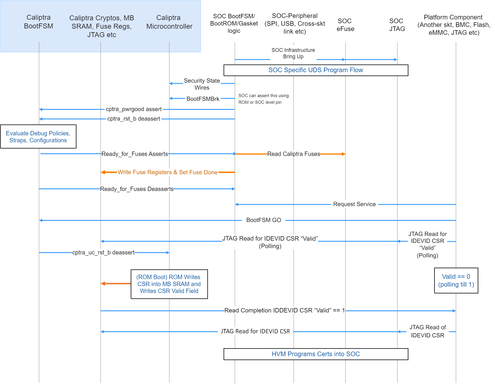
Figure 5: Device manufacturing identity flow
- High Volume Manufacturing (HVM) programs the IDevID certificate attributes fuses. See IDevID Certificate for encodings.
- HVM programs NIST compliant UDS into fuses using SoC-specific fuse programming flow. Note that this UDS goes through an obfuscation function within Caliptra IP.
- SoC drives the security state, which indicates that it's a manufacturing flow. See Caliptra Security States for encodings.
- SoC (using a GPIO pin or SoC ROM) drives BootFSMBrk (this is also used for debug cases). This can be driven at any time before cptra_rst_b is deasserted.
- SoC follows the boot flow as defined in Caliptra IP HW boot flow to assert cptra_pwrgood and deassert cptra_rst_b, followed by writing to the fuse registers.
- HVM, through JTAG or using the Caliptra SoC interface, sets “CPTRA_DBG_MANUF_SERVICE_REG” bit 0 to request a CSR.
- HVM, through JTAG or using the Caliptra SoC interface, writes to “CPTRA_BOOTFSM_GO” to allow Caliptra’s internal BootFSM to continue to bring up microcontroller out of reset.
- ROM reads the manufacturing state encoding from the “CPTRA_DBG_MANUF_SERVICE_REG” register, acquires the mailbox lock, and populates the Caliptra internal SRAM (the mailbox SRAM hardware structure is reused) with the CSR.
- HVM, through JTAG or using the SoC interface, polls for the “IDevID CSR ready" bit 24 that is set in “CPTRA_FLOW_STATUS” register.
- HVM reads mbox_status[3:0] to check if the data is ready to be read (DATA_READY encoding).
- HVM must clear bit 0 of CPTRA_DBG_MANUF_SERVICE_REG, indicating that it completed reading the CSR.
- Caliptra ROM opens the Caliptra Mailbox for SoC usages, such as FW loading (if required in some HVM flows). The SoC is only allowed to request a lock of the APB-exposed mailbox interface after this CSR operation is complete.
Certificate format
Caliptra certificates follow the X.509 v3 format described in RFC 5280. After vendor provisioning, Caliptra's certificate chain contains the following certificates:
- Provisioner CA (may be one or more certificates)
- IDevID
- LDevID
- AliasFMC
- AliasRT
- DPE
After owner provisioning, an Owner CA may endorse the IDevID, LDevID, or AliasFMC public keys. Owner CA provisioning is outside the scope of this specification.
Caliptra generates the LDevID, AliasFMC, AliasRT, and DPE certificates. The vendor, and optionally the owner, generate all other certificates.
Serial number algorithm
Caliptra uses certificate templates to avoid implementing fully capable X.509 v3 parsers and generators. Templates require certificates to be fixed length. This imposes constraints on the certificate serial numbers:
- Positive integer
- First octet as non-zero
- 20 octets in length
All Caliptra certificate serial numbers are generated with the following algorithm. The input is the certificate ECDSA public key in uncompressed form:
- Convert to DER format.
- Compute SHA256 digest.
- AND the least-significant-byte with ~0x80.
- OR the least-significant-byte with 0x04.
- Perform byte-wise copies of the least-significant 20 bytes into the certificate template.
Provisioner CA
Provisioner CA (pCA) is a set of one or more certificates issued by the vendor. The vendor is responsible for provisioning pCA to the SoC. Caliptra does not consume pCA. See Reference 5 for guidance on pCA.
IDevID certificate
The vendor issues the IDevID certificate during SoC manufacturing. As part of provisioning IDevID during manufacturing, Caliptra uses the UDS to derive the IDevID key pair and generate a CSR. The vendor's pCA uses the CSR to generate and sign the IDevID certificate. The CSR uses the format defined in PKCS#10.
For IDevID to endorse LDevID, Caliptra requires the vendor to implement an X.509 v3 IDevID certificate described in RFC 5280 with the field values specified in Table 7: IDevID certificate fields. The vendor shall also populate all extensions from the "Requested Extensions" attribute in the CSR. It is also recommended that the vendor add the Authority Information Access (AIA) extension to the IDevID certificate and maintain an Online Certificate Status Protocol (OCSP) responder with a URL pointed to by the AIA extension.
Table 7: IDevID certificate fields
| Field | Sub field | Value |
|---|---|---|
| Version | v3 | 2 |
| Serial Number | - | Generate with serial number algorithm using IDevID public key in uncompressed form |
| Validity | notAfter | 99991231235959Z |
| Subject Name | CN | Caliptra 1.0 IDevID |
| serialNumber | Hex-encoded printable string of SHA256 hash of DER-formatted IDevID public key in uncompressed form | |
| Subject Public Key Info | Algorithm | ecdsa-with-SHA384 |
| Parameters | Named Curve = prime384v1 | |
| Public Key | IDevID Public Key value | |
| Signature Algorithm Identifier | Algorithm | ecdsa-with-SHA384 |
| Parameters | Named Curve = prime384v1 | |
| Signature Value | - | Digital signature for the certificate |
| KeyUsage | keyCertSign | 1 |
| Basic Constraints | CA | TRUE |
| pathLen | 5 | |
| Subject Key Identifier | - | specified by IDevID attribute fuses |
| tcg-dice-Ueid | ueid | UEID specified by IDevID attribute fuses |
Caliptra does not consume the IDevID certificate. Caliptra needs attributes of the IDevID certificate in order to generate the Authority Key Identifier extension for the LDevID and to populate the TCG Universal Entity ID (UEID) extension for Caliptra-generated certificates. The vendor must fuse these attributes into the IDevID attribute fuses for Caliptra to consume. The encoding of these attribute fuses is as follows:
- Flags (byte 0, bits [1:0]): Key ID algorithm for IDevID Subject Key Identifier.
- 0 = SHA1 of DER-formatted IDevID public key in uncompressed form
- 1 = First 20 bytes of SHA256 of DER-formatted IDevID public key in uncompressed form
- 2 = First 20 bytes of SHA384 of DER-formatted IDevID public key in uncompressed form
- 3 = raw
- Reserved (bytes 1 to 3)
- Subject Key ID (bytes 4 to 23): if Flags = 3, the IDevID Subject Key Identifier to use as the LDevID Authority Key Identifier.
- UEID type (byte 24): UEID type as defined in IETF RATS specification. Used for TCG UEID extension.
- Reserved (bytes 25 to 27)
- Manufacturer Serial Number (bytes 28 to 43): the 128-bit unique serial number of the device to be used for the TCG UEID extension in the Caliptra-generated LDevID, AliasFMC, and AliasRT certificates.
The IDevID certificate is unique for each device and non-renewable. The SoC must be able to retrieve the IDevID certificate at runtime. To save flash space and aid in recoverability, it is recommended that the vendor define an IDevID certificate template such that the SoC at runtime can reconstruct the same certificate that the pCA endorsed. The SoC is recommended to store the IDevID certificate signature in fuses and the IDevID certificate template in the firmware image. Caliptra runtime firmware provides APIs to aid in reconstructing the certificate:
- GET_IDEV_INFO to return the IDevID public key.
- GET_IDEV_CERT to return the certificate given a to-be-signed (TBS) payload and the certificate signature from fuses. The TBS is the certificate template already patched with the IDevID public key, Subject Key Identifier, serial number, and any extensions that are unique to the device that the vendor may have included.
Caliptra does not allocate fuses in its fuse map for the IDevID certificate signature. Caliptra allocates "IDEVID MANUF HSM IDENTIFIER" fuses that the vendor can use to aid certificate reconstruction.
LDevID certificate
Caliptra ROM generates the LDevID certificate and endorses it with the IDevID private key. The LDevID certificate implements the following field values:
Table 8: LDevID certificate fields
| Field | Sub field | Value |
|---|---|---|
| Version | v3 | 2 |
| Serial Number | - | Generate with serial number algorithm using LDevID public key in uncompressed form |
| Issuer Name | CN | Caliptra 1.0 IDevID |
| serialNumber | Hex-encoded printable string of SHA256 hash of DER-formatted IDevID public key in uncompressed form | |
| Validity | notBefore | 20230101000000Z |
| notAfter | 99991231235959Z | |
| Subject Name | CN | Caliptra 1.0 LDevID |
| serialNumber | Hex-encoded printable string of SHA256 hash of DER-formatted LDevID public key in uncompressed form | |
| Subject Public Key Info | Algorithm | ecdsa-with-SHA384 |
| Parameters | Named Curve = prime384v1 | |
| Public Key | LDevID Public Key value | |
| Signature Algorithm Identifier | Algorithm | ecdsa-with-SHA384 |
| Parameters | Named Curve = prime384v1 | |
| Signature Value | - | Digital signature for the certificate |
| KeyUsage | keyCertSign | 1 |
| Basic Constraints | CA | True |
| pathLen | 4 | |
| Subject Key Identifier | - | First 20 bytes of SHA256 hash of DER-formatted LDevID public key in uncompressed form |
| Authority Key Identifier | - | specified by IDevID attribute fuses |
| tcg-dice-Ueid | ueid | UEID specified by IDevID attribute fuses |
Caliptra does not generate an LDevID CSR. Owners that wish to endorse LDevID must do so with proprietary flows.
AliasFMC certificate
Caliptra ROM generates the AliasFMC certificate and endorses it with the LDevID private key. The AliasFMC certificate implements the following field values:
Table 9: AliasFMC certificate fields
| Field | Sub field | Value |
|---|---|---|
| Version | v3 | 2 |
| Serial Number | - | Generate with serial number algorithm using FMC Alias public key in uncompressed form |
| Issuer Name | CN | Caliptra 1.0 LDevID |
| serialNumber | Hex-encoded printable string of SHA256 hash of DER-formatted LDevID public key in uncompressed form | |
| Validity | notBefore | notBefore from firmware manifest |
| notAfter | notAfter from firmware manifest | |
| Subject Name | CN | Caliptra 1.0 FMC Alias |
| serialNumber | Hex-encoded printable string of SHA256 hash of DER-formatted FMC Alias public key in uncompressed form | |
| Subject Public Key Info | Algorithm | ecdsa-with-SHA384 |
| Parameters | Named Curve = prime384v1 | |
| Public Key | FMC Alias Public Key value | |
| Signature Algorithm Identifier | Algorithm | ecdsa-with-SHA384 |
| Parameters | Named Curve = prime384v1 | |
| Signature Value | - | Digital signature for the certificate |
| KeyUsage | keyCertSign | 1 |
| Basic Constraints | CA | True |
| pathLen | 3 | |
| Subject Key Identifier | - | First 20 bytes of SHA256 hash of DER-formatted FMC Alias public key in uncompressed form |
| Authority Key Identifier | - | First 20 bytes of SHA256 hash of DER-formatted LDevID public key in uncompressed form |
| tcg-dice-Ueid | ueid | UEID specified by IDevID attribute fuses |
| tcg-dice-MultiTcbInfo | Flags | NOT_CONFIGURED if lifecycle is unprovisioned |
| NOT_SECURE if lifecycle is manufacturing | ||
| DEBUG if not debug locked | ||
| SVN | concatenation of FMC SVN and FMC fuse SVN | |
| FWIDs | [0] SHA384 digest of | |
| lifecycle state | ||
| debug locked state | ||
| anti-rollback disable fuse | ||
| ECDSA vendor public key index fuse | ||
| LMS vendor public key index fuse | ||
| LMS verification enable fuse | ||
| boolean indicating whether owner public key hash is in fuses | ||
| vendor public key hash | ||
| owner public key hash | ||
| [1] SHA384 digest of FMC |
Caliptra does not generate an AliasFMC CSR. Owners that wish to endorse AliasFMC must do so with proprietary flows.
AliasRT certificate
Caliptra FMC generates the AliasRT certificate and endorses it with the AliasFMC private key. The AliasRT certificate implements the following field values:
Table 10: AliasRT certificate fields
| Field | Sub field | Value |
|---|---|---|
| Version | v3 | 2 |
| Serial Number | - | Generate with serial number algorithm using RT Alias public key in uncompressed form |
| Issuer Name | CN | Caliptra 1.0 FMC Alias |
| serialNumber | Hex-encoded printable string of SHA256 hash of DER-formatted FMC Alias public key in uncompressed form | |
| Validity | notBefore | notBefore from firmware manifest |
| notAfter | notAfter from firmware manifest | |
| Subject Name | CN | Caliptra 1.0 Rt Alias |
| serialNumber | Hex-encoded printable string of SHA256 hash of DER-formatted RT Alias public key in uncompressed form | |
| Subject Public Key Info | Algorithm | ecdsa-with-SHA384 |
| Parameters | Named Curve = prime384v1 | |
| Public Key | RT Alias Public Key value | |
| Signature Algorithm Identifier | Algorithm | ecdsa-with-SHA384 |
| Parameters | Named Curve = prime384v1 | |
| Signature Value | - | Digital signature for the certificate |
| KeyUsage | keyCertSign | 1 |
| Basic Constraints | CA | True |
| pathLen | 2 | |
| Subject Key Identifier | - | First 20 bytes of SHA256 hash of DER-formatted RT Alias public key in uncompressed form |
| Authority Key Identifier | - | First 20 bytes of SHA256 hash of DER-formatted FMC Alias public key in uncompressed form |
| tcg-dice-Ueid | ueid | UEID specified by IDevID attribute fuses |
| tcg-dice-TcbInfo | SVN | RT SVN |
| FWIDs | [0] SHA384 digest of RT |
Caliptra does not generate an AliasRT CSR. Owners that wish to endorse AliasRT must do so with proprietary flows.
DPE certificate
Caliptra RT generates the DPE certificate and endorses it with the AliasRT private key. The DPE certificate fields are described in the Caliptra Runtime specification. DPE also supports issuance of CSRs.
Caliptra security states
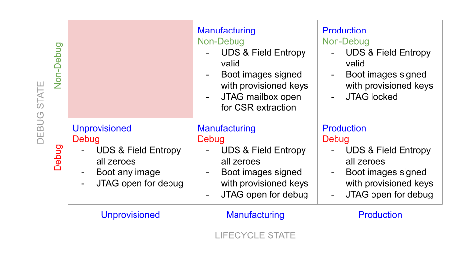
Figure 6: Caliptra security states
Definitions
- Non-Debug: Caliptra JTAG is not open for microcontroller and HW debug. Alias: DebugLocked
- Debug: Caliptra JTAG is open for microcontroller and HW debug. Alias: DebugUnlocked
- Unprovisioned: Blank/unprogrammed fuse part.
- Manufacturing: Device is in the manufacturing flow where HVM Caliptra fuses are programmed.
- Production: All of Caliptra’s HVM fuses are programmed.
- Secure: Any security state that restricts access to Caliptra from an external entity and has a known, specified function in the device lifecycle. Requires DebugLocked and either the Manufacturing or Production configuration.
- Insecure: Any security state other than those deemed secure. This includes all undefined states, all states with DebugUnlocked, and the Unprovisioned state. In accordance with the threat model, these states are considered a potential risk due to attacks via DFT or DFD channels, exploitation of unforeseen logic issues, or undefined behavior. These insecure states necessitate flushing of Caliptra secrets.
Notes:
- Caliptra’s security state is determined by the SoC’s security state and the SoC device lifecycle state.
- Caliptra’s state is considered a mode of operation.
- Caliptra security state is defined by the uppermost bit of the encoding below; 1=DebugLocked and 0=DebugUnlocked.
- Lower 2 bits are mapped to device lifecycle (unprovisioned, manufacturing, production).
- SoC’s security state may also be influenced by its own device lifecycle. A HW state machine must drive the SoC security state.
- Caliptra’s security state determines Caliptra’s debug state and the state of its security assets.
- In general, if Caliptra is in an insecure state, all keys and assets are ‘zeroized’. Zeroized may mean switching to all 0s, 1s, or debug keys based on the key. See Caliptra Assets for information.
Table 11: Security states
| Security state, device lifecycle state [2:0] | State | Definition | State transition requirement |
|---|---|---|---|
| 000b | DebugUnlocked and unprovisioned | This shall be the default state value for Caliptra’s security state; it is used for development and early Caliptra bring up. This state is not used to provision the Caliptra assets. In this state: - UDS and all other identity critical assets shall not be programmed in fuses. Un-programmed fuse bits shall be read as 0s (zero). The debug UDS shall be obfuscated and de-obfuscated using the debug obfuscation key. - Obfuscation key: The debug obfuscation key shall be used. - Caliptra JTAG is unlocked and allows microcontroller debug. - Caliptra JTAG can access IP internal registers through FW. | Unprovisioned to any other state requires a cold boot of Caliptra and SoC. |
| 101b | DebugLocked and manufacturing | Caliptra must be placed in this state during the secure HVM process. In this state: - UDS and other identity critical assets shall be programmed into fuses. They are written into Caliptra fuse registers, similar to the ‘Secure’ state. - All security assets shall be in production mode (production UDS and obfuscation shall be used). - Upon pwrgood assertion, Caliptra JTAG shall be locked; microcontroller debug shall be disabled. - Caliptra microcontroller can be interrupted through JTAG mailbox. | Manufacturing -> insecure state transition is allowed with warm reset and Caliptra clears all of the security critical assets and registers before JTAG is opened. Manufacturing -> secured state is allowed ONLY with a cold boot. See Provisioning During Manufacturing for details. |
| 111b | DebugLocked and production | All security assets are in production mode. In this state: - Production UDS and obfuscation key shall be used. - CPU execution shall be enabled. - All ‘backdoor’ functionality shall be disabled (for example, developer functions and functionality that could reveal sensitive information or result in escalation of privileges). - Debug functions shall be disabled. Caliptra JTAG is locked – microcontroller debug shall be disabled. Caliptra microcontroller shall not be interruptible through JTAG mailbox. - DFT functions shall be disabled. | DebugLocked -> DebugUnlocked will ONLY open JTAG with a cold or warm reset. A reset that triggers DebugUnlocked entry will also trigger clearing all of the security critical assets. |
| 011b | DebugUnlocked and production | This state is used when debugging of Caliptra is required. When in this state: UDS and other identity critical assets are programmed into fuses. They may not have been written into Caliptra fuse registers if the insecure state entered before Caliptra is out of reset. If the insecure state transition happened after fuses are written to Caliptra, they are cleared when the security state transitions from secure/production -> insecure. Caliptra state: All security assets are in debug mode (UDS and obfuscation key are in production state). - UDS: Reverts to a ‘well-known’ debug value. - Obfuscation key: Switched to debug key. - Key Vault is also cleared. - Caliptra JTAG is unlocked and allows microcontroller debug. - Caliptra JTAG can access IP internal registers through FW or directly. | DebugUnlocked -> DebugLocked is allowed ONLY with a cold boot. |
Notes:
- End-of-life state is owned by SoC. In end-of-life device lifecycle state, Caliptra shall not not be brought out of reset.
- Other encodings are reserved and always assumed to be in a secure state.
Each of these security states may be mapped to different SoC level debug and security states. SoC’s requirement is that if the SoC enters a debug state, then Caliptra must also be in an unsecured state where all assets are cleared. Caliptra security state is captured by hardware on every warm reset; therefore SoC integrators enforce the security state transition policies for cold boot events. These policies are described in the preceding table.
Service surface
The service surface of Caliptra has multiple vectors. All use cases are control plane services, useful to power on a system or start a task. Supporting line rate high performance IO cryptography or any other data path capability is not required.
- Logic IOs: Required to indicate status of the IP, availability of a message through APB, and to enable or disable certain debug capabilities (like JTAG enable or disable).
- Command mailbox: Caliptra shall offer services to other parts of the SoC. The APIs are documented in the Caliptra Runtime specification and summarized below:
- Loading firmware: Caliptra firmware is loaded via the mailbox at cold boot. In addition, Caliptra firmware can be loaded at runtime to support hitless or impactless updates.
- DICE-as-a-Service: Caliptra shall expose the TCG DICE Protection Environment iRoT Profile API, allowing Caliptra to derive and wield a DICE identity on behalf of other elements within the SoC. For example, Caliptra can sign messages for an SPDM responder.
- Measurement Vault: Caliptra shall support stashing of measurements for the code and configuration of the SoC. Caliptra can provide these measurements via PCR Quote API or via DPE.
- FW Authentication: Caliptra supports ECDSA verification for SoC firmware beyond its own. The SHA384 block exposes a HW API for hashing firmware. The runtime firmware exposes an ECDSA verification API that uses the hash computed by the SHA384 block.
Device resilience
As noted earlier, Caliptra plays a role in maintaining the resilience posture of the SoC as defined by NIST SP 800-193 Platform Firmware Resiliency Guidelines (see Reference 1). As the Silicon RTM and RTI, Caliptra is either responsible for, or participates in, various protection and detection requirements described in the NIST publication.
The following table describes the NIST SP 800-193 requirements that Caliptra shall meet, either on its own or in conjunction with other components within the SoC or platform. Requirements not listed are assumed to be not covered and out-of-scope for Caliptra. In particular, most requirements related to firmware update and recovery are out-of-scope and must be handled by other components of the system.
Table 12: NIST SP 800-193 requirements
| NIST SP 800-193 Chapter | Requirement | Caliptra responsibility |
|---|---|---|
| 4.1.1 | All security mechanisms and functions shall be founded to Roots of Trust (RoT). | Caliptra forms the basis for all trust in the SoC starting from execution of its immutable ROM. See the Secure Boot Flow section. |
| 4.1.1 | If Chains of Trust (CoT) are used, RoT shall serve as the anchor for the CoT. | Caliptra firmware shall be authenticated and executed as part of a Chain of Trust extended from the Caliptra ROM, while all other firmware shall be measured into a CoT extended from the Caliptra ROM. See the Secure Boot Flow section. |
| 4.1.1 | All RoTs and CoTs shall either be immutable or protected using mechanisms that ensure all RoTs and CoTs remain in a state of integrity. | Caliptra firmware is authenticated and executed as part of a Chain of Trust extended from the Caliptra ROM. See the Secure Boot Flow section. The SoC or platform is responsible for maintaining integrity for other elements of the CoT. |
| 4.1.1 | All elements of the CoT for update, detection, and recovery in non-volatile storage shall be implemented in platform firmware. | Caliptra forms the basis for RTM, which the SoC can use to create detection capabilities. All other silicon RoT capabilities are extended by additional firmware loaded in the SoC and anchored by Caliptra. |
| 4.1.1 | The functions of the RoTs or CoTs shall be resistant to any tampering attempted by software running under, or as part of, the operating system on the host processor. | Caliptra shall run on a dedicated microcontroller, isolated physically from access by other components in the system. |
| 4.1.1 | Information transferred from the software on the host processor to the platform firmware shall be treated as untrusted. | Caliptra shall verify the authenticity of its firmware using an approved digital signature verification mechanism. |
| 4.1.1 | CoTs may be extended to include elements that are not from non-volatile storage. Before use, those elements shall be cryptographically verified by an earlier element of the CoT. | Caliptra shall verify the authenticity of its firmware using an approved digital signature verification mechanism. Caliptra shall also collect the measurement of the SoC security processor FMC code before it is verified and executed by the SoC. |
| 4.1.2 | If the key store is updateable, then the key store shall be updated using an authenticated update mechanism, absent unambiguous physical presence through a secure local update. | Hashes for the keys used to authenticate Caliptra FW are programmed into fuses during manufacturing. If a key is deemed to be compromised, that key may be revoked and the next key used instead. |
| 4.1.3 | Each platform device that implements a detection capability shall rely on either a Root of Trust for Detection (RTD), or a Chain of Trust for Detection (CTD). The CTD is anchored by an RTD for its detection. | Caliptra forms the basis for RTM, which the SoC can use to create detection capabilities. Caliptra firmware shall be authenticated and executed as part of a Chain of Trust extended from the Caliptra ROM, while all other firmware shall be measured into a CoT extended from the Caliptra ROM. See the Secure Boot Flow section. |
| 4.1.3 | The RTD or CTD shall include or have access to information necessary to detect corruption of firmware code and critical data. | Caliptra relies on hashes of authorized keys stored in fuses. Those hashes are then checked against public keys found in firmware headers to authenticate Caliptra’s runtime firmware. Caliptra relies on redundancy in the fuses to protect the key and configuration data. |
| 4.2.3 | If critical platform firmware code in non-volatile memory is copied into RAM to be executed (for performance, or for other reasons) then the firmware program in RAM shall be protected from modification by software or shall complete its function before software starts. | Caliptra shall run on a dedicated microcontroller, isolated physically from access by other components in the system. |
| 4.2.3 | If critical platform firmware uses RAM for temporary data storage, then this memory shall be protected from software running on the platform until the data’s use is complete. | Caliptra shall run on a dedicated microcontroller, isolated physically from access by other components in the system. |
| 4.2.3 | Software shall not be able to interfere with the intended function of critical platform firmware. For example, by denying execution, modifying the processor mode, or polluting caches. | Caliptra shall run on a dedicated microcontroller, isolated physically from access by other components in the system. In addition, the Caliptra subsystem begins execution before other firmware is allowed to run. |
| 4.2.4 | Critical data shall be modifiable only through the device itself or defined interfaces provided by device firmware. Examples of defined interfaces include proprietary or public application programming interfaces (APIs) used by the device’s firmware, or standards-based interfaces. Symbiont devices may rely on their host devices to meet this requirement. | Caliptra receives firmware and configuration input only via defined interfaces within the SoC. See the Mailbox section. |
| 4.2.1.3 | The authenticated update mechanism shall be capable of preventing unauthorized updates of the device firmware to an earlier authentic version that has a security weakness or would enable updates to a version with a known security weakness. | Caliptra supports a mechanism for detecting and preventing execution of a prior firmware image that is no longer authorized. See the Anti-rollback Support section. |
| 4.3.1 | A successful attack that corrupts the active critical data or the firmware image, or subverts their protection mechanisms, shall not in and of itself result in a successful attack on the RTD or the information necessary to detect corruption of the firmware image. | Caliptra shall verify the signature of any firmware it loads during each boot. If the signature verification fails, Caliptra shall notify the SoC that firmware recovery must be performed. See the Error Reporting and Handling section. |
| 4.3.1 | Verify integrity, using an approved digital signature algorithm or cryptographic hash, of device firmware code prior to execution of code outside the RTD. | Caliptra shall perform digital signature verification of its firmware before it is allowed to execute. |
| 4.3.1 | If firmware corruption is detected, the RTD or CTD should be capable of starting a recovery process to restore the device firmware code back to an authentic version. | Caliptra shall notify the SoC via the Mailbox interface to initiate the recovery process. |
| 4.3.1 | The detection mechanism should be capable of creating notifications of firmware corruption. | Caliptra shall notify the SoC via the Mailbox interface to initiate the recovery process. |
| 4.3.1 | The detection mechanism should be capable of logging events when firmware corruption is detected. | It is the responsibility of the SoC to log any corruption events upon notification by Caliptra. |
| 4.3.2 | The RTD or CTD shall perform integrity checks on the critical data prior to use. Integrity checks may take the form, for example, of validating the data against known valid values or verifying the hash of the data storage. | Caliptra relies on SoC fuse integrity to store its configuration data, which is owned and passed to Caliptra through the Mailbox. |
| 4.3.2 | The RTD or CTD should be capable of creating notifications of data corruption. | See the Error Reporting and Handling section. |
| 4.3.2 | The detection mechanism should be capable of logging events when data corruption is detected. | It is the responsibility of the SoC to log any corruption events upon notification by Caliptra. |
Secure boot flow
Caliptra shall follow and implement the secure boot guidelines as described in Reference 3.
For the detailed flow, see the hardware section and firmware verifcation section.
Hitless update
A ‘hitless’ (aka ‘impactless’) update occurs when an update is applied to Caliptra’s executing firmware without requiring a SoC or machine reboot. A hitless update allows Caliptra FW4 to remain up to date with FW security and/or functional patches while preventing or reducing machine downtime. Hitless update shall take effect immediately upon application (post-cryptographic verification). Updates to the machine’s persistent storage are still required because they ensure that Caliptra reboots to the latest FW if the system requires a restart or reboot.
Caliptra contains multiple hardware isolated registers for Platform Configuration Registers (PCR). These PCRs serve as volatile storage for concise cryptographic measurement of security state, including Caliptra’s own firmware.
Journey measurements matter because hitless updates are a challenge for devices that only capture their current firmware version and state. This is particularly true when the previous state may have impacted the current state of dependent components within the SoC. For example, a device might move from firmware version A to firmware version B without assuming a clean start to flush state. Vulnerabilities in firmware version A might impact version B. Preserving a device boot measurement and currently running measurement can highlight differences, but preserving these measurements does not distinguish between transitional states, such as when intermediate updates have the potential to expose the device to vulnerabilities. For example, a device may move from firmware version A, to B, and then to C without a restart, whereas another device of the same type might transition from A to C without transitioning through B. If tracking only the boot and current firmware version, should a vulnerability be found in version B, it is impossible to identify which devices transitioned through B compared to devices that transitioned from A to C directly.
To capture all firmware and configuration changes, Caliptra tracks and attests to both current measurements and cumulative measurement PCR banks. The current measurement is a snapshot of the currently running firmware and configuration. This provides easy reference for the current version. If the current and cumulative measurements are different, it can safely be assumed that the device has undergone some update. The cumulative measurement captures all of the firmware and state transitions from a clean cold boot to the current version. The cumulative measurement must be accompanied by a log structure that describes the path from boot to current measurement using hash extensions. A verifier can understand a device’s path to its current state by replaying log entries to reconstruct the cumulative measurement.
The log and cumulative measurement mechanism is similar to that used in TPM. In this model, Caliptra only needs to securely manage the measurements; the log does not need to be secured or maintained by Caliptra or the SoC. The construction of measurements through cryptographic hash extensions means that the log must provide the exact order and evidence needed to reconstruct the measurement. As such, the log is tamper evident by design and does not need to be kept secure.
Caliptra contains 32 384-bit PCR banks that are extendable by the SHA engine, and readable by Caliptra firmware. The usage of the PCR banks is as follows:
Table 13: PCR bank usage
| PCR number | Type | Extend control | Description |
|---|---|---|---|
| PCR0 | Current | ROM | Holds Caliptra’s FMC measurement and ROM policy configuration. |
| PCR1 | Cumulative | ROM | Holds journey of Caliptra’s FMC measurement and ROM policy configuration. |
| PCR2 | Current | FMC | Holds Caliptra's runtime firmware and firmware manifest measurements. |
| PCR3 | Cumulative | FMC | Holds journey of Caliptra's runtime firmware and firmware manifest measurements. |
| PCR4 to PCR30 | - | RT | Holds measurements extended by EXTEND_PCR commands (serviced by RT). |
| PCR31 | Cumulative | ROM | Holds measurements extended by STASH_MEASUREMENTS commands (serviced by both ROM and RT). |
For PCR0 and PCR1, ROM issues the following extend operations in order:
- An array containing the following fields as 8-bit values:
- Lifecycle state
- Debug locked state
- Anti-rollback disable fuse
- ECDSA vendor public key index
- FMC SVN
- Effective Fuse SVN (i.e., 0 if anti-rollback disable is set)
- LMS vendor public key index
- LMS verification enable fuse
- Boolean indicating whether the owner public key hash is in fuses
- Vendor public key hash
- Owner public key hash
- Digest of FMC
Caliptra ROM fails to boot if the following values do not remain constant across a hitless update:
- Owner public key hash
- ECDSA vendor public key index
- LMS vendor public key index
- FMC digest
Attestation of Caliptra's update journey
Upon every cold boot and hitless update, Caliptra ROM extends Caliptra's FMC measurement and ROM policy configuration into PCR0 (current) and PCR1 (cumulative). Upon every cold boot and hitless update, Caliptra FMC extends Caliptra's runtime firmware and firmware manifest measurements into PCR2 (current) and PCR3 (cumulative). The current measurement of the FMC, ROM policy configuration, RT, and FW manifest are used to derive a CDI and an alias key given to runtime firmware. FMC places runtime firmware's measurements into runtime firmware's alias key certificate, and signs that certificate with FMC's alias key.
When runtime firmware boots following a hitless update, it will use the following pieces of data for building the DPE nodes and certificate chain:
- Its CDI, derived by FMC
- Its alias key, generated by FMC
- Its alias certificate, signed by FMC
- Its journey measurements in PCR3, extended by FMC
- SRAM state, established by the prior runtime firmware image
SRAM state consists of measurements captured by prior runtime firmware images, and does not contain secrets or executable data5. Therefore, the trustworthiness of runtime firmware is reflected in the measurements captured by FMC and is evident in the runtime firmware alias certificate.
Caliptra firmware will attest to PCR3 by including it as an input in all DPE leaf key derivations and as evidence in all DPE leaf key certificates.
Commentary: recovery from a bad hitless update
Suppose the following Caliptra firmware images exist:
- Version A: presumed-good
- Version B: known-bad
- Version C: presumed-good
A remote verifier wishes to confirm that a given Caliptra device has not run version B since cold boot. The remote verifier can challenge the SoC with a freshness nonce; higher-layer software passes that freshness nonce as a request to Caliptra's DPE for signing. The remote verifier receives the following pieces of evidence:
- An endorsement over LDevID, which may take a number of forms, including:
- Caliptra's vendor-signed certificate over IDevID, and an IDevID-signed certificate over LDevID.
- An owner-signed certificate over IDevID, and an IDevID-signed certificate over LDevID.
- An owner-signed certificate over LDevID.
- An LDevID-signed certificate over AliasFMC, which includes FMC's measurements as captured by ROM.
- An AliasFMC-signed certificate over AliasRT, which includes runtime firmware's measurements as captured by FMC.
- An AliasRT-signed certificate over a leaf DPE key, which includes PCR3 as read by runtime firmware, along with other measurements previously stashed in SRAM.
- A log structure6 that represents the measurements that have been extended into PCR3.
- A leaf-DPE-signed blob7 containing the freshness nonce.
The remote verifier evaluates (1) according to ownership policies to determine whether the Caliptra device is trustworthy, before proceeding to verify the rest of the attestation response.
Thus satisfied in the trustworthiness of the Caliptra device, the remote verifier can then evaluate the trustworthiness of FMC by inspecting the measurements in (2), AliasFMC's certificate. The verifier can reject the attestation if those measurements do not conform to a known-good value.
Thus satisfied in the trustworthiness of FMC, the remote verifier can then evaluate the trustworthiness of runtime firmware by inspecting the measurements in (3), AliasRT's certificate. If version A or C is running, then the PCR3 measurement present in (4), the leaf DPE key certificate, is presumed to be an honest reflection of the hardware register as read by runtime firmware. The verifier can reject the attestation if AliasRT's certificate indicates that version B is currently running.
Thus satisfied that version B is not currently running and that PCR3 is an accurate reflection of the hardware register, the remote verifier can then compare the log in (5) to PCR3 in (4) to confirm its authenticity, then walk the log to confirm that FMC never launched version B since cold-boot. If version B did run, that firmware could have maliciously modified DPE measurements stashed in SRAM, but could not have modified the contents of PCR3 to erase the evidence that version B ran at all, and could not have influenced the behavior of firmware versions A or C to prevent them from accurately reporting the contents of PCR3.
Thus satisfied that version B has not run since power-on, the verifier can also optionally inspect other measurements in (4) to evaluate the journey of other SoC components, whose measurements were previously stored within Caliptra's SRAM.
Finally, the verifier can confirm freshness by comparing the nonce in (6) to the one emitted in the original challenge. Because DPE only allows a derived leaf key to be used if the measurements present in its leaf certificate are a reflection of the current state, the fact that the freshness nonce was signed by DPE is evidence that the measurements in (4) are fresh.
Commentary: maintaining sealed secrets across a power cycle
Caliptra does not seal secrets directly. However, Caliptra does implement DPE, which allows secrets to be sealed to an external sealer such as a TPM, with a policy that only allows those secrets to be unsealed if Caliptra allows the host to wield a particular leaf DPE key. This leaf DPE key is permuted based on the hitless update journey of the various components whose measurements are stored within Caliptra.
This poses a challenge for maintaining sealed secrets across a power cycle. Suppose the SoC cold booted CPU microcode A, then hitlessly updated to B, and then to C. The measurements stored within Caliptra's SRAM will represent the [A->B->C] update journey, and DPE's leaf key is derived based on this journey.
Let us assume that upon each hitless update, the firmware update is also written to persistent storage, such that on the next cold boot the new firmware will run. Thus, on the next boot, the SoC's microcode update journey is simply [C]. This is a different journey than [A->B->C], and so DPE's leaf key will differ. The old secret sealed to the old DPE leaf key is no longer accessible to the SoC.
To anticipate this eventuality, before a power cycle, the SoC can instruct DPE to predict what the DPE leaf public key will be if the microcode journey is simply [C], using DPE's simulation context. The SoC can then reseal secrets to the external sealer with a policy that can be satisfied if the computed public key is used.
Note: as all DPE leaf keys are derived using Caliptra runtime firmware's CDI, a DPE simulation context cannot predict the leaf key that would be available if a different Caliptra firmware image were to boot (because one Caliptra firmware image does not have access to a different image's CDI). Therefore, if a different Caliptra firmware image is staged to persistent storage, Caliptra must first be hitlessly updated to that image before a simulation context can be used to predict public keys that will be available to that image on the next cold boot.
Attestation of SoC update journey
Caliptra shall also attest to the journeys of SoC components. A SoC component's journey may change independently of other components. For example, SoC components may implement partial resets or hitless updates that cause the component's firmware or configuration to reload.
Caliptra shall maintain a reboot counter for each component. Caliptra shall increment the reboot counter and update the journey measurement for calls that indicate that the component's state changed. Caliptra shall attest the journey measurement and report the counter value on-demand. The verifier is assumed to have knowledge of update events at an associated reboot counter (via an event log) but not have knowledge of reset events. The verifier can compute the journey measurement via multiplicatively extending the current measurement by the reset counter. For example:
- Upon cold boot, SoC component boots firmware A. Reboot counter is 0. The tuple of (0,A) is in the event log.
- SoC component is partial reset once. Reboot counter is 1.
- SoC component is hitlessly updated to firmware B. Reboot counter is 2. The tuple of (2,B) is in the event log.
- SoC component is partial reset twice. Reboot counter is 4.
The corresponding journey measurement computation is the chained extension of [A->A->B->B->B]. The verifier can ascertain this through the two event log entries.
Anti-rollback support
Caliptra shall provide fuse banks (refer to Table 19: Caliptra Fuse Map) that are used for storing monotonic counters to provide anti-rollback enforcement for Caliptra mutable firmware. Each distinctly signed boot stage shall be associated with its own anti-rollback fuse field. Together with the vendor, Caliptra allows owners to enforce strong anti-rollback requirements, in addition to supporting rollback to a previous firmware version. This is a critical capability for hyper scalar owners.
Every mutable Caliptra boot layer shall include a SVN value in the signed header. If a layer's signed SVN value is less than the current counter value for that layer's fuse bank, Caliptra shall refuse to boot that layer, regardless of whether the signature is valid.
Alternatively, platform vendors may prefer to manage firmware storage and rollback protection in a different manner, such as through a dedicated Platform RoT. In such cases, the vendor may wish to disable anti-rollback support from Caliptra entirely. This disable support is available via an OTP/fuse setting.
Each of Caliptra's internal anti-rollback fuse banks shall support a minimum counter value of 64. This feature is expected to be used sparingly.
Physical attack countermeasures
Caliptra shall implement countermeasures designed to deter both glitching (also referred to fault-injection (FI)) and side-channel attacks (simple power analysis (SPA) and differential power analysis (DPA)).
The Caliptra threat model guides the priority of which physical countermeasures are based on a specific physical implementation.
From the top, an adversary in the supply chain has essentially unlimited time to glitch the chip and make it reveal any private key material or symmetric secrets. One Glitch To Rule Them All is one example with recency bias. The most critical countermeasures must prevent non-destructive extraction of those secrets. Otherwise, an adversary who succeeds can silently impersonate production-serving assets at a later time.
Randomly generated per-part entropy is subject to physical inspection attacks in the supply chain as well. The fuses that store the UDS entropy shall be protected to a degree that forces an attacker to perform a destructive operation to read their values. Decapping and fibbing attacks should at least penetrate enough layers and metal shielding to render the part useless, if not being outright impossible to carry out. Entropy tied to a damaged asset typically requires injection of counterfeit devices in the supply chain, which is a very powerful adversary model.
Another way to obtain access to secret entropy with “unlimited supply chain time” is to observe side channels while the SoC is executing. Because Caliptra is expected to be a <1 mm2 fraction of a large SoC, side-channel mitigation is required only against extremely resourceful attackers that can wade through and discern a large number of confounding signals and power profiles. With that priority in mind, DPA and DMA attacks should be mitigated via decoy value generation.
Any private key material or symmetric key material embedded in the RTL (and therefore “global”) must be treated as having low value, reaching zero value in a number of quarters. A supply chain attacker can destructively obtain the key material, and loss of one part is not going to trigger any alarms.
Mitigation against SCA is not trivial and may be implemented in a variety of ways. Reference 7 provides a comprehensive overview of methods and techniques used in various SCA as well as recommendations for countermeasures against such attacks (including feasibility and applicability). Additionally, there are academic papers available from NIST and other resources that discuss SCA and their countermeasures.
Compliance and certification requirements
Due to the identity service surface offered to other SoC subsystems, Caliptra may fall under the Target of Evaluation (ToE) of an application that wishes to attain a specific compliance level for business reasons.
It is important to highlight that it’s not necessary for the RTM itself to unilaterally attain (for example, FIPS 140-3 L3). It is only relevant when the RTM is included in the “bag” that wants to obtain a compliance certification. For example, it is relevant when a cloud provider wants to FIPS-certify PCIe link encryption in transit rooted to an ASIC identity emanating from a Caliptra instance.
See Reference 8 for requirements related to keys, entropy, random bits, cryptographic modules, and algorithms.
Known Answer Test (KAT) support
To certify a cryptographic module, pre-operational self-tests must be performed when the system is booted. Implementing KATs is required for FIPS certification. However, regardless of FIPS certification, it is considered a security best practice to ensure that the supported cryptographic algorithms are functioning properly to guarantee correct security posture.
KAT execution is described as two types:
- Pre-operational Self-Test (POST)
- Conditional Algorithm Self-Test (CAST)
A detailed description of the POST and CAST KATs can be found at csrc.nist.gov.
Table 14: KAT failure mitigations
| KAT type | If fails |
|---|---|
| POST | Failure of a POST KAT (for example, ECDSA) shall result in Caliptra boot failure. A reset may or may not result in successful POST completion. |
| CAST | Failure of a CAST KAT shall cause Caliptra to fail any operation that has a dependency on the associated cryptographic algorithm. |
Table 15: POST/CAST usage
| Crypto algorithm | Caliptra Boot ROM | Caliptra FMC | Caliptra Runtime FW |
|---|---|---|---|
| ECDSA8 | Yes | Yes | Yes |
| AES | Yes | No | No |
| SHA9 | Yes | Yes | Yes |
| DRBG | No | No | No |
| HMAC | Yes (CDI generation) | No | No |
| KDF | Yes | Yes | No |
As shown in Table 15: POST/CAST usage, since the cryptographic algorithms required by the Caliptra Boot ROM are considered POSTs, and those same algorithms are used by Caliptra FMC and FW, there is no requirement that FMC and Runtime FW implement CASTs for those algorithms.
Firmware image format and verification
Caliptra supports verifying firmware with ECDSA P384 signatures and Leighton-Micali Hash-based Signatures (LMS) in accordance with the requirements described in Reference 3.
Caliptra firmware is composed of two images: an FMC image and an application firmware image. A single firmware manifest describes these images. The manifest consists of a preamble (Table 16), a header (Table 17), and a Table of Contents (TOC) (Table 18). The image layout is shown in Figure 7: firmware image layout.

Figure 7: Firmware image layout
To verify the firmware, Caliptra ROM performs the following steps:
- Calculates the hash of the vendor public keys in the preamble and compares it against the hash in fuses (key_manifest_pk_hash). If the lifecycle is not "unprovisioned" and the hashes do not match, the boot fails.
- Calculates the hash of the owner public keys in the preamble and compares it against the hash in fuses (owner_pk_hash). If the owner_pk_hash fuse is not zero (i.e., unprovisioned) and hashes do not match, the boot fails. See the Owner authorization section.
- Ensures the vendor public key(s) selected by the preamble indices are not revoked based on fuse: key_manifest_pk_hash_mask for ECDSA public key, lms_revocation for LMS public key.
- Calculates the hash of the first byte through the vendor data field of the header (this includes the TOC digest). This is the vendor firmware digest.
- Calculates the hash of the first byte through the owner data field of the header (this includes the TOC digest). This is the owner firmware digest.
- Verifies the vendor signature using the vendor firmware digest from step 4 and the vendor key(s) from step 3.
- Verifies the owner signature using the owner firmware digest from step 5 and the owner key(s) from step 2.
- Verifies the TOC against the TOC digest that was verified in steps 6 and 7. The TOC contains the SVNs and digests for the FMC and runtime images.
- Verifies the FMC against the FMC digest in the TOC.
- If Caliptra is not in "unprovisioned" lifecycle state or "anti-rollback disable" state, ROM compares the FMC SVN against FMC SVN fuse (fuse_key_manifest_svn).
- Verifies the runtime against the runtime digest in the TOC.
- If Caliptra is not in "unprovisioned" lifecycle state or "anti-rollback disable" state, ROM compares the runtime digest against the runtime SVN fuse (fuse_runtime_svn).
In addition to cold boot, Caliptra ROM performs firmware verification on hitless updates. See the hitless update section for details.
Table 16: Firmware manifest preamble
Fields are little endian unless described otherwise.
| Field | Size (bytes) | Description |
|---|---|---|
| Firmware Manifest Marker | 4 | Magic Number marking the start of the package manifest. The value must be 0x434D414E (‘CMAN’ in ASCII) |
| Firmware Manifest Size | 4 | Size of the full manifest structure |
| Vendor ECDSA Public Key 1 | 96 | ECDSA P384 public key used to verify the Firmware Manifest Header Signature. X-Coordinate: Public Key X-Coordinate (48 bytes, big endian) Y-Coordinate: Public Key Y-Coordinate (48 bytes, big endian) |
| Vendor ECDSA Public Key 2 | 96 | ECDSA P384 public key used to verify the Firmware Manifest Header Signature. X-Coordinate: Public Key X-Coordinate (48 bytes, big endian) Y-Coordinate: Public Key Y-Coordinate (48 bytes, big endian) |
| Vendor ECDSA Public Key 3 | 96 | ECDSA P384 public key used to verify the Firmware Manifest Header Signature. X-Coordinate: Public Key X-Coordinate (48 bytes, big endian) Y-Coordinate: Public Key Y-Coordinate (48 bytes, big endian) |
| Vendor ECDSA Public Key 4 | 96 | ECDSA P384 public key used to verify the Firmware Manifest Header Signature. X-Coordinate: Public Key X-Coordinate (48 bytes, big endian) Y-Coordinate: Public Key Y-Coordinate (48 bytes, big endian) |
| Vendor LMS Public Key 1 | 48 | LMS public key used to verify the Firmware Manifest Header Signature. tree_type: LMS Algorithm Type (4 bytes, big endian) Must equal 12. otstype: LM-OTS Algorithm Type (4 bytes, big endian) Must equal 7. id: (16 bytes) digest: (24 bytes) |
| Vendor LMS Public Key 2 | 48 | LMS public key used to verify the Firmware Manifest Header Signature. tree_type: LMS Algorithm Type (4 bytes, big endian) Must equal 12. otstype: LM-OTS Algorithm Type (4 bytes, big endian) Must equal 7. id: (16 bytes) digest: (24 bytes) |
| . . | ||
| Vendor LMS Public Key 32 | ||
| ECDSA Public Key Index Hint | 4 | The hint to ROM to indicate which ECDSA public key it should first use. |
| LMS Public Key Index Hint | 4 | The hint to ROM to indicate which LMS public key it should first use. |
| Vendor ECDSA Signature | 96 | Vendor ECDSA P384 signature of the Firmware Manifest header hashed using SHA384. R-Coordinate: Random Point (48 bytes, big endian) S-Coordinate: Proof (48 bytes, big endian) |
| Vendor LMS Signature | 1620 | Vendor LMS signature of the Firmware Manifest header hashed using SHA384. q: Leaf of the Merkle tree where the OTS public key appears (4 bytes) ots: LM-OTS Signature (1252 bytes) tree_type: LMS Algorithm Type (4 bytes, big endian) Must equal 12. tree_path: Path through the tree from the leaf associated with the LM-OTS signature to the root. (360 bytes) |
| Owner ECDSA Public Key | 96 | ECDSA P384 public key used to verify the Firmware Manifest Header Signature. X-Coordinate: Public Key X-Coordinate (48 bytes, big endian) Y-Coordinate: Public Key Y-Coordinate (48 bytes, big endian) |
| Owner LMS Public Key | 48 | LMS public key used to verify the Firmware Manifest Header Signature. tree_type: LMS Algorithm Type (4 bytes, big endian) Must equal 12. otstype: LM-OTS Algorithm Type (4 bytes, big endian) Must equal 7. id: (16 bytes) digest: (24 bytes) |
| Owner ECDSA Signature | 96 | Vendor ECDSA P384 signature of the Firmware Manifest header hashed using SHA384. R-Coordinate: Random Point (48 bytes, big endian) S-Coordinate: Proof (48 bytes, big endian) |
| Owner LMS Signature | 1620 | Owner LMS signature of the Firmware Manifest header hashed using SHA384. q: Leaf of the Merkle tree where the OTS public key appears (4 bytes) ots: LM-OTS Signature (1252 bytes) tree_type: LMS Algorithm Type (4 bytes, big endian) Must equal 12. tree_path: Path through the tree from the leaf associated with the LM-OTS signature to the root. (360 bytes) |
| Reserved | 8 | Reserved 8 bytes |
Table 17: Firmware manifest header
Fields are little endian unless described otherwise.
| Field | Size (bytes) | Description |
|---|---|---|
| Revision | 8 | 8-byte version of the firmware image bundle |
| Vendor ECDSA public key index | 4 | The hint to ROM to indicate which ECDSA public key it should first use. |
| Vendor LMS public key index | 4 | The hint to ROM to indicate which LMS public key it should first use. |
| Flags | 4 | Feature flags. Bit0: - Interpret the pl0_pauser field. If not set, all PAUSERs are PL1 Bit1-Bit31: Reserved |
| TOC Entry Count | 4 | Number of entries in TOC. |
| PL0 PAUSER | 4 | The PAUSER with PL0 privileges. This value is used by the RT FW to verify the caller privilege against its PAUSER. The PAUSER is wired through APB. |
| TOC Digest | 48 | SHA384 Digest of table of contents. |
| Vendor Data | 40 | Vendor Data. Not Before: Vendor Start Date [ASN1 Time Format] for Caliptra-issued certificates (15 bytes) Not After: Vendor End Date [ASN1 Time Format] for Caliptra-issued certificates (15 bytes) Reserved: (10 bytes) |
| Owner Data | 40 | Owner Data. Not Before: Owner Start Date [ASN1 Time Format] for Caliptra-issued certificate. Takes precedence over vendor start date (15 bytes) Not After: Owner End Date [ASN1 Time Format] for Caliptra-issued certificates. Takes precedence over vendor end date (15 bytes) Reserved: (10 bytes) |
Table 18: Table of contents
Fields are little endian unless described otherwise.
| Field | Size (bytes) | Description |
|---|---|---|
| TOC Entry Id | 4 | TOC Entry ID. The fields can have the following values: 0x0000_0001: FMC 0x0000_0002: Runtime |
| Image Type | 4 | Image Type that defines the format of the image section 0x0000_0001: Executable |
| Image Revision | 20 | Git Commit hash of the build |
| Image Version | 4 | Firmware release number |
| Image SVN | 4 | Security Version Number for the Image. This field is compared against the fuses (FMC SVN or runtime SVN). |
| Image Minimum SVN | 4 | Minimum Security Version Number for the Image. This field is compared against the fuses (FMC SVN or runtime SVN). |
| Image Load Address | 4 | Load address |
| Image Entry Point | 4 | Entry point to start the execution from |
| Image Offset | 4 | Offset from beginning of the image |
| Image Size | 4 | Image Size |
| Image Hash | 48 | SHA384 hash of image |
Post-Quantum Cryptography (PQC) requirements
Recent guidance from the US Government, CNSA 2.0, requests the use of LMS by 2025. Caliptra has an option to require LMS signatures in addition to ECDSA signatures (vendor and owner).
Based on the recommendation in CNSA 2.0, Caliptra uses the SHA256/192 algorithm. To provide a balance between the number of signatures allowed and signature size, Caliptra uses an LMS tree height of 15. This is referred to in NIST SP 800-208 as the LMOTS_SHA256_N24_W4 and LMS_SHA256_M24_H15 parameter sets.
Caliptra supports 32 LMS trees for the vendor and 1 tree for the owner. The SoC can support multiple trees for the owner via ownership transfer. It is recommended that the LMS trees are created from multiple HSMs that are geographically distributed.
Key rotation
Firmware signing key rotation shall follow the requirements described in Reference 3.
Hardware
The following figure describes the Caliptra Core.
Figure 8: Caliptra Core block diagram
- Memory requirements:
- 128 KiB of ICCM0
- 128 KiB for Mailbox as a staged SRAM (for FW staging of impactless updates to do authentication checks on the FW before moving to ICCM)
- 128 KiB for DCCM and 48 KiB for ROM
- Cryptography requirements:
- SHA256, SHA384, and SHA512
- ECDSA Secp384r1 with HMAC-DRBG - key generation, signing and verification
- HMAC SHA384
- AES256-CBC
- Chips Alliance is used for RISC-V.
- APB is the choice for the SoC-facing interface.
- JTAG is exported at the IP interface.
- TRNG is the digital logic and algorithms that are required for random number generation. It requires a physical entropy source input. See the Caliptra IP specification and integration specification for more information.
- For SoCs that want to use their own legacy TRNG, Caliptra provides a HW API to push the random number on the request/response handshake. See the Caliptra IP specification and integration specification for more information. This mode is advised for early development but discouraged for production tape outs due to the lower security assurances of an external TRNG.
The following figure describes the Caliptra IP HW boot flow.
Figure 9: Hardware boot flow
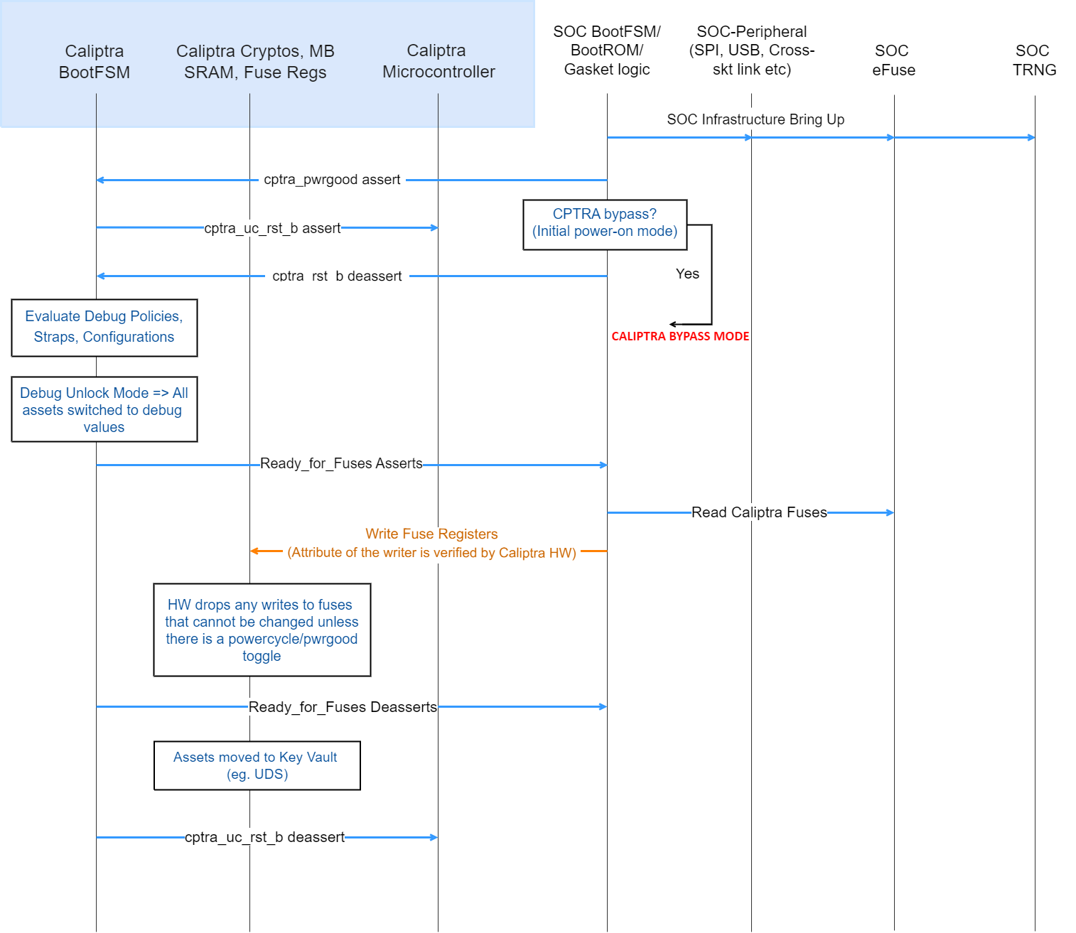
- As part of the SoC boot flow, SoC may have other infrastructure and entities that boot. That part of the flow is outside the scope of this document. If SoC chooses to bypass Caliptra, then it should have a capability to bypass Caliptra entirely through its proprietary flow. This may be needed for initial power-on and other early validation.
- Cptra_pwrgood is asserted to the Caliptra IP block.
- Cptra_rst_b is deasserted to the Caliptra IP block. See the integration specification for guidelines on the minimum number of cycles between these two signals.
- Caliptra IP now evaluates the strap settings driven through various interface wires (for example, the security or debug state of the SoC).
- If SoC is in a debug mode, then security assets are cleared or switched to debug mode.
- Caliptra IP asserts Ready_For_Fuse wire to the SoC.
- The SoC populates the fuse registers, the internal TRNG configuration registers, and the ROM WDT cycle count, then sets the CPTRA_FUSE_WR_DONE bit. Note that Caliptra HW drops writes to any registers that cannot be changed unless there is a power cycle (for example, UDS). So SoC is free to write all the registers.
- Caliptra IP deasserts Ready_for_Fuse wire as soon as the fuse write done register is written.
- Caliptra IP moves security critical assets in fuse registers (for example, UDS) to the key vault.
Caliptra FW push flow
Figure 10: FW push flow
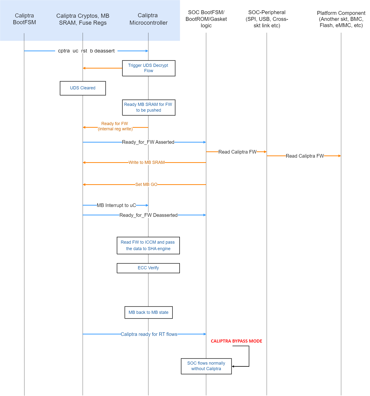
- After the Caliptra microcontroller is out of reset, ROM starts executing and triggers the crypto block to run the UDS decrypt flow.
- Caliptra ROM enables the mailbox. (Until this point, any accidental or non-accidental writes that target the mailbox are dropped by the hardware.)
- Caliptra ROM asserts READY_FOR_FW wire. This is done by writing an internal register. This register is also visible to read on the APB interface. SoC can choose to poll on this bit instead of using the wire (it is the SoC integration choice).
- SoC follows the mailbox protocol and pushes Caliptra FW into the mailbox.
- Caliptra’s mailbox HW asserts an interrupt to the microcontroller after the GO is written, per mailbox protocol. See Mailbox for specifics.
- After Caliptra’s FW is authenticated and loaded into ICCM, microcontroller runs the firmware and asserts READY_FOR_RTFLOWS wire.
CPU warm reset or PCIe hot reset flow → Caliptra IP reset
Figure 11: Hardware reset flow
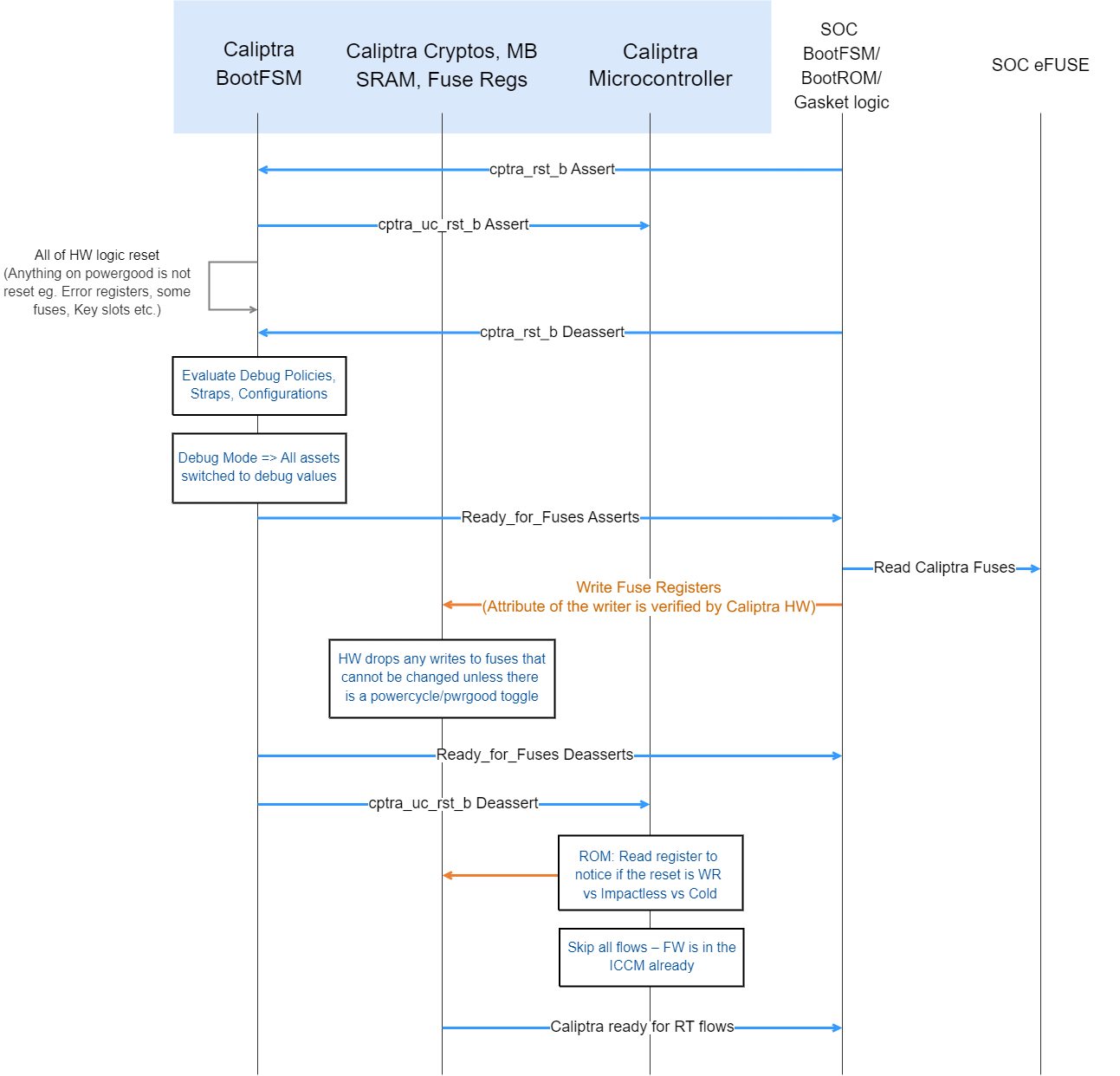
Note: Since Caliptra IP may be placed in an ACPI S5 domain of the device, there may be devices where Caliptra IP may not go through reset on a device hot reset or CPU warm reset. But the flow shows what happens when such a reset happens.
- Caliptra IP’s reset is asserted by the SoC.
- Caliptra’s internal BootFSM resets the microcontroller and then resets all of the logic (including the SoC-facing APB interface). Only registers or flops that are sitting on powergood are left with the same value. Note that SRAMs do not have a reset.
- Caliptra IP’s reset is deasserted by the SoC.
- At this point, the HW boot flow is the same as the cold boot flow. SoC is required to configure the internal TRNG and ROM WDT and then set CPTRA_FUSE_WR_DONE. This causes Caliptra IP to deassert the Ready_for_Fuse wire.
- Caliptra’s ROM reads an internal register to differentiate between warm, cold, and impactless flow. If it's a warm reset flow, then it skips DICE key generation and FW load flows (because keys were already derived and FW is already present in ICCM). This is an important reset time optimization for devices that need to meet the hot reset specification time.
Because warm reset is a pin input to Caliptra, Caliptra may not be idle when a warm reset occurs. If a warm reset occurs while Caliptra ROM, FMC, or RT initialization code is executing, Caliptra may be inoperable until a subsequent cold reset. If a warm reset occurs while Caliptra runtime is servicing a request, Caliptra shall remain operable but may refuse to wield production assets for subsequent requests.
Note: The cold reset flow is not explicitly mentioned but it is the same as the cold boot flow because Caliptra IP has no state through a cold reset.
Mailbox
The Caliptra Mailbox is a 128 KiB buffer that is used to exchange data between the SoC and the Caliptra microcontroller.
The SoC communicates with the mailbox over an APB interface. This allows the SoC to identify the device that is using the interface. This ensures that the mailbox, control registers, and fuses are read or written only by the appropriate device.
When a mailbox is populated by SoC, an interrupt to the FW occurs. This indicates that a command is available in the mailbox. The microcontroller is responsible for reading from and responding to the command.
When a mailbox is populated by the microcontroller, Caliptra sends a wire indication to the SoC that a command is available in the mailbox as well as updating the MAILBOX STATUS register. The SoC is responsible for reading from and responding to the command.
Mailboxes are generic data passing structures, and the Caliptra hardware only enforces the protocol for writing to and reading from the mailbox. How the command and data are interpreted by the FW and SoC are not enforced in Caliptra.
Sender protocol
Sending data to the mailbox:
- Requester queries the mailbox by reading the LOCK control register.
- If LOCK returns 0, LOCK is granted and is set to 1.
- If LOCK returns 1, MBOX is locked for another device.
- Requester writes the command to the COMMAND register.
- Requester writes the data length in bytes to the DLEN register.
- Requester writes data packets to the MBOX DATAIN register.
- Requester writes to the EXECUTE register.
- Requester reads the STATUS register until a value other than CMD_BUSY is detected. This is also indicated by a dedicated wire that asserts when STATUS is changed. STATUS can return:
- DATA_READY – Indicates the return data is in the mailbox for the requested command.
- CMD_COMPLETE – Indicates the successful completion of the requested command.
- CMD_FAILURE – Indicates the requested command failed.
- CMD_BUSY – Indicates the requested command is still in progress.
- If response data is expected and the requester reads a STATUS of DATA_READY:
- Requester reads from the DLEN register to ascertain the size of the response data.
- Requester reads data from the DATAOUT register until DLEN bytes are read.
- After reading the response data, if any, requester writes 0 to the EXECUTE register to clear LOCK.
Notes on behavior: After LOCK is granted, the mailbox is locked until that device has concluded its operation. The mailbox is responsible only for accepting writes from the device that requested and locked the mailbox.
Figure 12: Mailbox sender flow
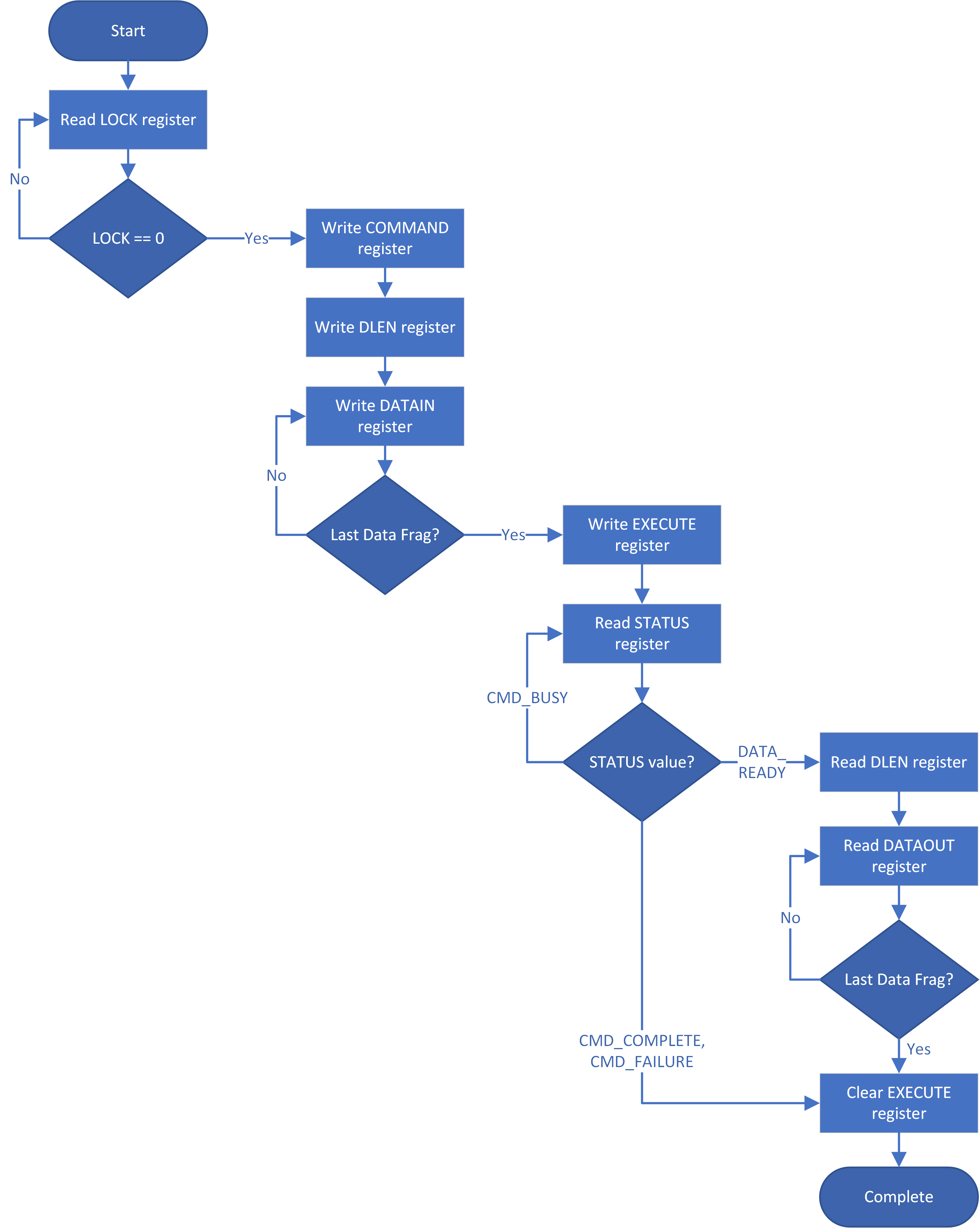
Receiver protocol
Upon receiving an indication that the mailbox is populated, the appropriate device can read the mailbox. This is indicated by a dedicated wire that is asserted when Caliptra populates the mailbox for SoC consumption.
Receiving data from the mailbox:
- Receiver reads the COMMAND register.
- Receiver reads the DLEN register.
- Receiver reads the MBOX DATAOUT register.
- Continues reading MBOX DATAOUT register until DLEN bytes are read.
- If response data is required:
- Receiver writes the size of the response data to the DLEN register.
- Receiver writes to the DATAIN register until DLEN bytes are written.
- Note: Response data is only supported for Caliptra, to SoC-initiated commands. SoC cannot provide response data for Caliptra-initiated commands.
- Receiver writes to the STATUS register.
- If response data was provided, STATUS should be written to DATA_READY.
- Otherwise, STATUS should be written to CMD_COMPLETE (or CMD_FAILURE).
Figure 13: Mailbox receiver flow
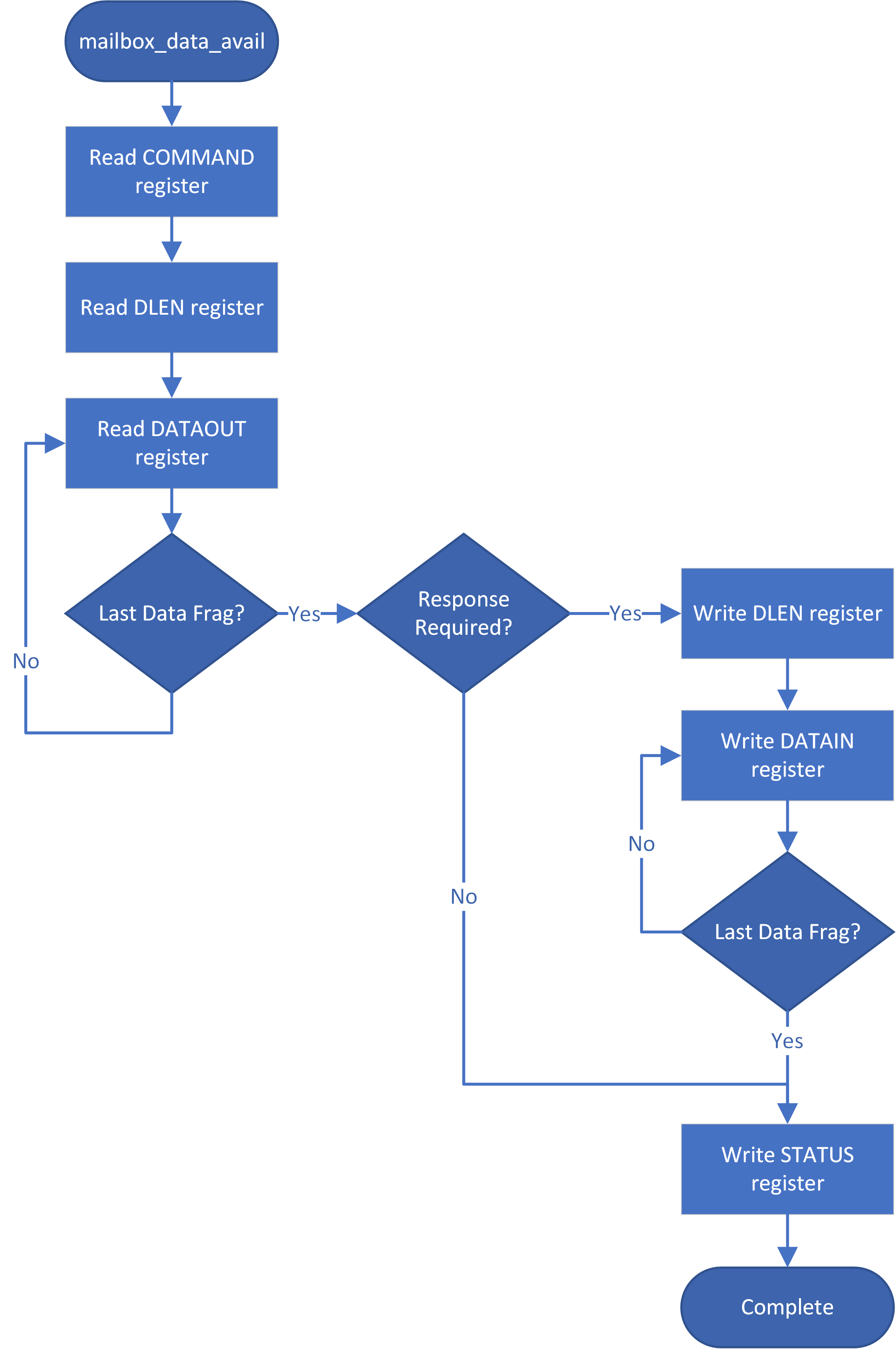
User attributes
The PAUSER field of the APB interface is used to encode device attributes for the requester that is utilizing the SoC interface. These values can be used for:
- Ensuring the device that was granted the LOCK is the one that accesses the MBOX, DLEN, COMMAND, and STATUS registers.
- Prioritizing who is next granted the LOCK.
Mailbox commands
The Caliptra mailbox commands are specified in the Caliptra runtime firmware specification.
Hash calculation HW API
Caliptra provides a HW API to do a SHA384 hash calculation. The SoC can access the accelerator through this hardware API and stream data to be hashed over the APB interface. The hash is captured into a register for SoC to use or Caliptra FW to be used for the Signature Authentication API.
JTAG/TAP debug
Figure 14: Debug flow
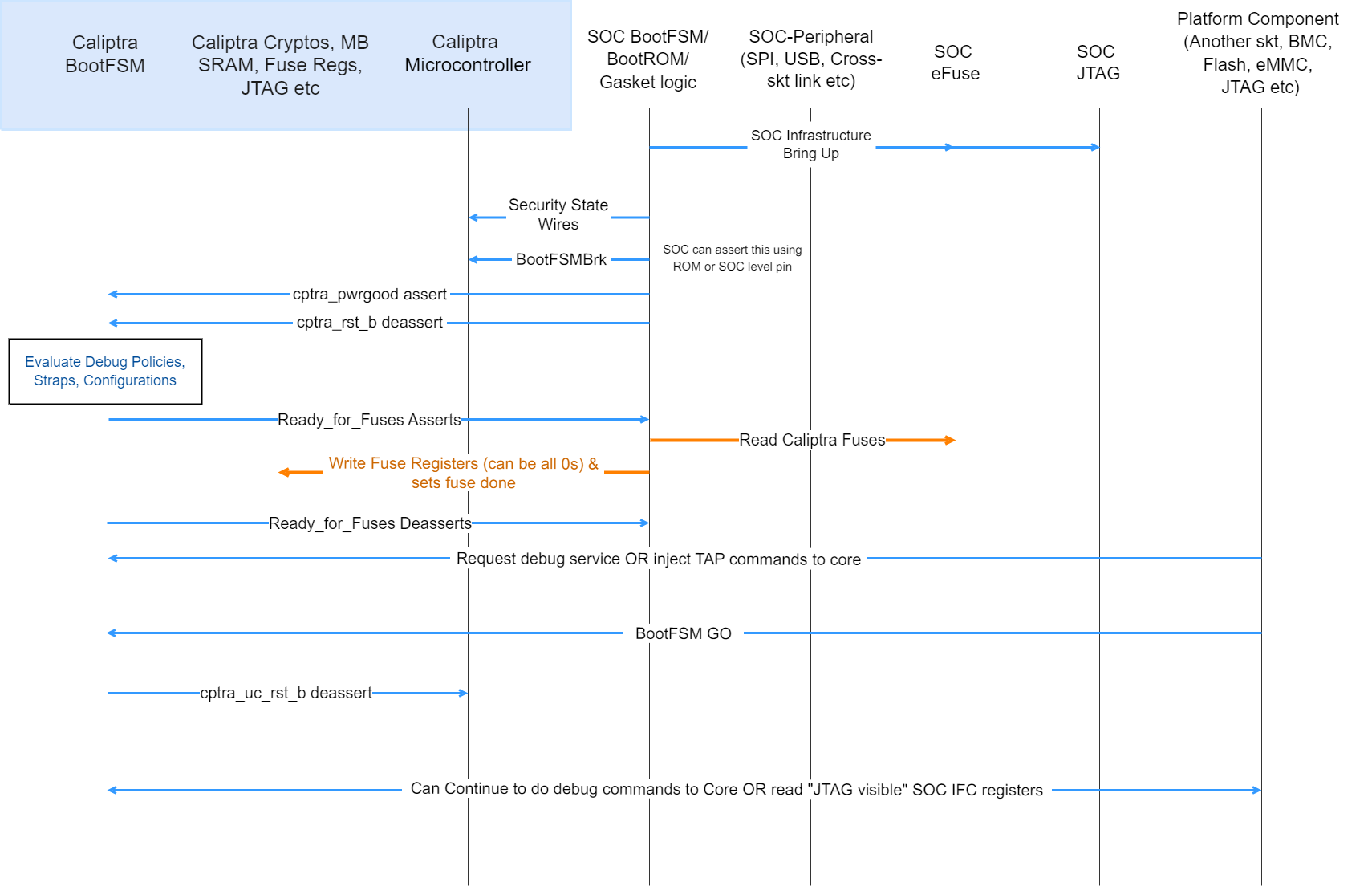
- SoC drives the security state indicating that it is a debug flow. See Caliptra security states for encodings.
- SoC (using a GPIO pin or SoC ROM) drives BootFSMBrk (this is also used for debug cases). This can be driven at any time before cptra_rst_b is deasserted.
- SoC follows the boot flow as defined in Caliptra IP HW boot flow to assert cptra_pwrgood and deassert cptra_rst_b, followed by writing to the fuse registers.
- HVM, through JTAG or through the Caliptra SoC interface, writes to “CPTRA_DBG_MANUF_SERVICE_REG”, requesting the appropriate debug service (see the ROM/Runtime specifications for bit definitions).
- HVM, through JTAG, can also inject microcontroller TAP commands at this point following the VeeR Specification.
- HVM, through JTAG or through the Caliptra SoC interface, writes to “CPTRA_BOOTFSM_GO” to allow Caliptra’s internal BootFSM to continue to bring up microcontroller out of reset.
- Microcontroller executes the appropriate debug service.
- Specific SoC interface registers (MBOX_DLEN, MBOX_DOUT, MBOX_STATUS, CPTRA_BOOT_STATUS, CPTRA_HW_ERRROR_ENC, CPTRA_FW_ERRROR_ENC, BOOTFSM_GO, CPTRA_DBG_MANUF_SERVICE_REG) are accessible over the JTAG interface in debug (or manufacturing mode). The following are the JTAG register addresses for these registers:
- DMI_REG_MBOX_DLEN = 7'h50; (Read-only)
- DMI_REG_MBOX_DOUT = 7'h51; (Read-only)
- DMI_REG_MBOX_STATUS = 7'h52; (Read-only)
- DMI_REG_BOOT_STATUS = 7'h53; (Read-only)
- DMI_REG_CPTRA_HW_ERRROR_ENC = 7'h54; (Read-only)
- DMI_REG_CPTRA_FW_ERROR_ENC = 7'h55; (Read-only)
- DMI_REG_CPTRA_DBG_MANUF_SERVICE_REG = 7'h60; (Read-Write)
- DMI_REG_BOOTFSM_GO = 7'h61; (Read-Write)
- Note: These are injected as TAP register read/write commands as defined in the VeeR Specification.
Notes:
- The security state is latched at cptra_rst_b deassertion. If the security state is unlocked at this time, only TAP is opened.
- Changing the security state at a random time after cptra_rst_b deassertion: does not unlock Caliptra JTAG.
- Changing the security state at a random time after cptra_rst_b deassertion: transition from debug locked to debug unlocked has no effect until next reset.
- Setting scan mode at a random time after cptra_pwrgood: flushes out all internal Caliptra secrets, assets, key vault, and crypto intermediate state.
- Scan mode assertion does not automatically open Caliptra JTAG.
Architectural registers
These registers are accessible over APB to be read according to the register access permissions. For more information, see the register reference manual at https://ereg.caliptra.org.
Fuse requirements
Fuse registers are programmable whenever IP goes through reset (after cptra_rst_b asserts and de-asserts) and before the fuse registers are locked from writes. If the lock was set, the writes are dropped. The lock is sticky across a warm reset.
To ensure that the security claims of Caliptra are achieved, specific fuse protection capabilities must be supported:
- Fuses that hold Caliptra secrets shall not be readable by any mutable code in the SoC. The intent is to provide defense-in-depth for the UDS.
- For SoCs that intend to achieve FIPS 140-3 CMVP certification with Caliptra, SoC shall implement a HW state machine for copying the uds_seed, field_entropy, and key_manifest_pk_hash fuses from the fuse controller into Caliptra's fuse shadow registers. Only the fuse controller, this state machine, and Caliptra shall be able to access these fuse values. The intent is to not include the SoC ROM as part of the cryptographic module boundary.
- For the production lifecycle state, if JTAG is enabled pre or post SoC reset, then Caliptra's dedicated fuses shall not be accessible (shall not be readable, shall not be writable) by Caliptra or other SoC IP. This restriction shall be applicable to Caliptra's fuse shadow registers as well (see Physical Attack Countermeasures).
- SoC should ensure that the integrity of each fuse is maintained through the life of the part. The integrity of the fuses can be maintained by fuse redundancy, ECC, or other means determined sufficient by the SoC.
Fuse programming
All fuse based cryptographic keying material and seeds (for example, UDS Seed) shall be generated (on-chip or off-chip) per requirements described in Reference 8.
SoC shall support in-field programmable fusing. Fuse Map shows which fuses are expected to be in-field programmable. SoCs shall implement authorization for in-field programmable fusing to mitigate denial-of-service attacks. Authorization design is outside the scope of this specification.
SoC shall support a field entropy programming API. The API shall support retrieving an input value from an external interface. It should cryptographically mix that value with the output of an on-die TRNG to generate the field entropy value. The API implementation shall burn the field entropy value into the first available field entropy fuse slot (or fail if no slots are available). Caliptra is expected to be in any security state. The device owner is expected to call this API in a “clean room environment” to minimize risk of attack on the programming process.
Fuse zeroing
Caliptra assumes that the unfused value in fuses is '0' and the fused value is '1'. With this context, zeroization refers to destroying a secret value by fusing it to all ones.
For SoCs that intend to achieve FIPS 140-3 CMVP certification with Caliptra:
- SoC shall implement zeroization for uds_seed and field_entropy such that the fuse rows holding these secrets contain all ones.
- SoC shall expose and document an API for a tester to invoke zeroization.
- SoC shall indicate that zeroization has occurred by statically asserting GENERIC_INPUT_WIRE[0] to Caliptra.
- SoC shall set Caliptra’s security state to DebugUnlock by ORing it with the zeroization status signal.
- SoC shall expose Caliptra architectural registers as API for a tester to read.
- SoC shall ensure authorization for this API to guard against denial-of-service attacks. The authorization design is left to the vendor.
Fuse map
The following table describes Caliptra's fuse map:
Table 19: Caliptra Fuse Map
| Name | Size (bits) | ACL | Fuse programming time | Description |
|---|---|---|---|---|
| UDS SEED (obfuscated) | 384 | ROM | SoC manufacturing | DICE Unique Device Secret Seed. This seed is unique per device. The seed is scrambled using an obfuscation function. |
| FIELD ENTROPY (obfuscated) | 256 | ROM | Device owner in-field programmable | Field-programmable by the owner, used to hedge against UDS disclosure in the supply chain. |
| KEY MANIFEST PK HASH | 384 | ROM FMC RUNTIME | SoC manufacturing | SHA384 hash of the Vendor ECDSA P384 and LMS Public Keys. |
| KEY MANIFEST PK HASH MASK | 4 | ROM FMC RUNTIME | In-field programmable | One-hot encoded list of revoked Vendor ECDSA P384 Public Keys. |
| OWNER PK HASH | 384 | ROM FMC RUNTIME | In-field programmable | SHA384 hash of the Owner ECDSA P384 and LMS Public Keys. |
| FMC KEY MANIFEST SVN | 32 | ROM FMC RUNTIME | In-field programmable | FMC security version number. |
| RUNTIME SVN | 128 | ROM FMC RUNTIME | In-field programmable | Runtime firmware security version number. |
| ANTI-ROLLBACK DISABLE | 1 | ROM FMC RUNTIME | SoC manufacturing or in-field programmable | Disables anti-rollback support from Caliptra. (For example, if a Platform RoT is managing FW storage and anti-rollback protection external to the SoC.) |
| IDEVID CERT IDEVID ATTR | 768, 352 used | ROM FMC RUNTIME | SoC manufacturing | IDevID Certificate Generation Attributes. See IDevID certificate section. Caliptra only uses 352 bits. Integrator is not required to back the remaining 416 bits with physical fuses. |
| IDEVID MANUF HSM IDENTIFIER | 128, 0 used | ROM FMC RUNTIME | SoC manufacturing | Spare bits for Vendor IDevID provisioner CA identifiers. Caliptra does not use these bits. Integrator is not required to back these with physical fuses. |
| LIFE CYCLE | 2 | ROM FMC RUNTIME | SoC manufacturing | Caliptra Boot Media Integrated mode usage only. SoCs that build with a Boot Media Dependent profile don’t have to account for these fuses. - '00 - Unprovisioned - '01 - Manufacturing - '10 - Undefined - '11 - Production Reset: Can only be reset on powergood. |
| LMS VERIFY | 1 | ROM | In-field programmable | - 0 - Verify Caliptra firmware images with ECDSA-only. - 1 - Verify Caliptra firmware images with both ECDSA and LMS. |
| LMS REVOCATION | 32 | ROM | In-field programmable | One-hot encoded list of revoked Vendor LMS Public Keys. |
| SOC STEPPING ID | 16 | ROM FMC RUNTIME | SoC manufacturing | Identifier assigned by vendor to differentiate silicon steppings. |
Error reporting and handling
This section describes Caliptra error reporting and handling.
Table 20: Hardware and firmware error types
| Fatal errors | Non-fatal errors | |
|---|---|---|
| Hardware | - ICCM, DCCM SRAM ECC. - The second watchdog (WD) timer expiry triggers an NMI, and a FATAL error is signaled to the SoC. - Operating HMAC, ECC, or DOE engines simultaneously. | - Mailbox SRAM ECC (except initial firmware load) - Mailbox incorrect protocol or commands. For example, incorrect access ordering or access without Lock. |
| Firmware | - Control Flow Integrity (CFI) errors. - KAT errors. - FIPS Self Test errors. - Mailbox commands received after FIPS Shutdown request completes. - Hand-off errors detected upon transfer of control from ROM to FMC or FMC to Runtime. - Mailbox protocol violations leading the mailbox to an inconsistent state if encountered by ROM during cold reset flow. - Firmware image verification or authentication failures if encountered by ROM during Cold Reset flow. - Non-aligned access to ICCM or DCCM - AHB access hangs, triggered through WD timer expiry - AHB access outside of the decoding range | - Firmware image verification or authentication failures if encountered by ROM during Update Reset flow. - Mailbox protocol violations leading the mailbox to an inconsistent state (if encountered by ROM during Update Reset flow). - Cryptography processing errors. |
Fatal errors
- Fatal errors log the FATAL ERROR reasons into an architectural register that is RW from the external world. This register must be sticky (as in, reset is on powergood).
- This register may be cleared at any time via register write (W1C).
- Caliptra signals fatal errors using a cptra_error_fatal wire.
- SoCs should connect this into their SoC error handling logic. Upon detection of a FATAL ERROR in Caliptra, SoC shall treat any outstanding commands with Caliptra as failed, and SoC may recover by performing a Caliptra reset using the signal
cptra_rst_b. - This signal prevents forward progress of the boot process if measurement submission to Caliptra fails. If SoC detects a Caliptra fatal error while the SoC is in steady state, then there is no obligation for the SoC to immediately address that error. If rebooting the SoC for such failures is deemed unacceptable to uptime, the SoC should implement the ability to trigger a Caliptra warm reset independently of the SoC, and may use this mechanism to recover.
- Error mask registers (writable only by Caliptra microcontroller) may be used to prevent error signal assertion per-event. Mask registers only impact interrupts when they are set prior to the error occurrence.
- cptra_error_fatal remains asserted until Caliptra is reset. Note that, although the HW FATAL ERROR register fields may be cleared at any time, a reset is still required to clear the interrupt.
- SoCs should connect this into their SoC error handling logic. Upon detection of a FATAL ERROR in Caliptra, SoC shall treat any outstanding commands with Caliptra as failed, and SoC may recover by performing a Caliptra reset using the signal
- When a fatal error occurs, all volatile assets that are stored in key vault are cleared.
Non-fatal errors
- Non-fatal errors log the NON-FATAL ERROR reasons into an architectural register that is RW from the external world. This register must be sticky (as in, reset is on powergood).
- This register may be cleared at any time via register write (W1C).
- Caliptra signals non-fatal errors using a cptra_error_non_fatal wire.
- Caliptra reset via
cptra_rst_b, or a write to clear the NON-FATAL ERROR register, cause the interrupt to deassert. - It is optional for SoCs to include this signal in their logic.
Firmware errors
Please refer to the Caliptra code base for a list of the error codes.
Future effort: Caliptra security subsystem
A future effort is a full security subsystem solution. This solution is a combination of fully open source digital logic and licensable analog components that are technology dependent, such as TRNG analog sources or technology dependent fuse controllers.
- SoC Controller has configurable SRAMs and reference firmware.
- SoC reference ROM allows for configurable initialization.
- Resource handling logic (RHL) brings up subsystem components such as PUF, PLL, Fuse controller, [P-]TRNG. etc. RHL processes requests from Caliptra to the outside components (for example, P-TRNG request input to Caliptra’s internal TRNG).
- Some of the analog components are licensable IPs that are used to build the subsystem (for example, PUF, and PLL).
Figure 15: Caliptra security subsystem
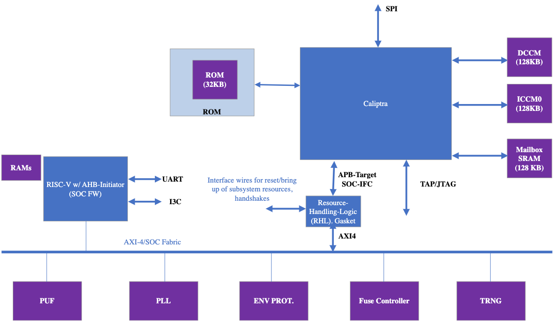
The Caliptra subsystem offers a complete RoT subsystem, with open source programmable components for customization of SoC boot flows.
Terminology
The following acronyms and abbreviations are used throughout this document.
References
- NIST Special Publication 800-193 Platform Firmware Resiliency Guidelines
- Global Platform Technology Root of Trust Definitions and Requirements Version 1.1 Public
- Open Compute Project Secure Boot Specification
- TCG DICE Layering Architecture Version 1.0 Revision 0.19 July 23, 2020
- TCG DICE Attestation Architecture Version 1.00 Revision 0.23 March 1, 2021
- TCG Hardware Requirements for a Device Identifier Composition Engine Family “2.0” Level
- Side-Channel Attacks: Ten Years After Its Publication and the Impacts on Cryptographic Module Security Testing
- Attestation of System Components v1.0 Requirements and Recommendations
- OCP Security WG: Ownership Transfer
Acknowledgments
The Caliptra Workgroup acknowledges the following individuals for their contributions to this specification.
CONTRIBUTORS
- Akash Singh (NVIDIA)
- Alex Tzonkov (AMD)
- Andrés Lagar-Cavilla (Google)
- Anjana Parthasarathy (Microsoft)
- Anthony Rocha (AMD)
- Avirup Mullick (NVIDIA)
- Bharat Pillilli (Microsoft)
- Bryan Kelly (Microsoft)
- Caleb Whitehead (Microsoft)
- Howard Tran (Google)
- Ishwar Agarwal (Microsoft)
- James Zhang (NVIDIA)
- Jeff Andersen (Google)
- John Traver (AMD)
- Jordan Hand (Google)
- Kor Nielsen (Google)
- Louis Ferraro (AMD)
- Marius Schilder (Google)
- Matt Cockrell (Google)
- Michael Norris (Microsoft)
- Nathan Nadarajah (AMD)
- Norman Stewart (AMD)
- Paul Chou (NVIDIA)
- Piotr Kwidzinski (AMD)
- Prabhu Jayana (AMD)
- Rob Strong (AMD)
- Sudhir Mathane (AMD)
- Stephanie Morton (Google)
- Steven Bellock (NVIDIA)
- Varun Sampath (NVIDIA)
- Vishal Soni (Microsoft)
- Vishal Mhatre (Microsoft)
Footnotes
Caliptra is Spanish for “root cap” and describes the deepest part of the root.
This obfuscation key may be a chip-class secret, or a chip-unique PUF, with the latter preferred.
This memory should only be volatile in a power loss event. See details in the reset flow section.
When a hitless update occurs, and then following reset, Caliptra shall execute the updated firmware and shall maintain the measurements that it collected during boot. Caliptra shall support the reporting of these measurements with signed attestations. Hitless update of Caliptra’s FMC shall not be supported. Hitless update requires creating a new DICE identity, which would require access to IDevID and LDevID. Retention of IDevID and LDevID (privkeys) during post-boot introduce a security vulnerability.
Upon boot, firmware defensively treats existing SRAM contents as potentially malicious, emplaced by prior firmware with a vulnerability.
The format of this log is outside the scope of this specification.
The format of this blob is outside the scope of this specification.
ECDSA is used for firmware verification and SPDM (signing).
SHA is used with ECDSA and HMAC, and is also used to generate measurements.
5f85fb4
![]()
Caliptra Hardware Specification
Version 1.1
Scope
This document defines technical specifications for a Caliptra RoT for Measurement (RTM)[1] cryptographic subsystem used in the Open Compute Project (OCP). This document, along with Caliptra: A Datacenter System on a Chip (SoC) Root of Trust (RoT), shall comprise the Caliptra technical specification.
Overview
This document provides definitions and requirements for a Caliptra cryptographic subsystem. The document then relates these definitions to existing technologies, enabling device and platform vendors to better understand those technologies in trusted computing terms.
Caliptra Core
For information on the Caliptra Core, see the High level architecture section of Caliptra: A Datacenter System on a Chip (SoC) Root of Trust (RoT).
Boot FSM
The Boot FSM detects that the SoC is bringing Caliptra out of reset. Part of this flow involves signaling to the SoC that Caliptra is awake and ready for fuses. After fuses are populated and the SoC indicates that it is done downloading fuses, Caliptra can wake up the rest of the IP by de-asserting the internal reset.
The following figure shows the initial power-on arc of the Mailbox Boot FSM.
Figure 1: Mailbox Boot FSM state diagram
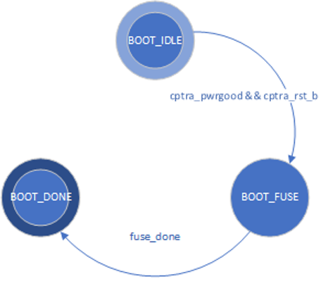
The Boot FSM first waits for the SoC to assert cptra_pwrgood and de-assert cptra_rst_b. In the BOOT_FUSE state, Caliptra signals to the SoC that it is ready for fuses. After the SoC is done writing fuses, it sets the fuse done register and the FSM advances to BOOT_DONE.
BOOT_DONE enables Caliptra reset de-assertion through a two flip-flop synchronizer.
FW update reset (Impactless FW update)
When a firmware update is initiated, Runtime FW writes to fw_update_reset register to trigger the FW update reset. When this register is written, only the RISC-V core is reset using cptra_uc_fw_rst_b pin and all AHB targets are still active. All registers within the targets and ICCM/DCCM memories are intact after the reset. Reset is deasserted synchronously after a programmable number of cycles; the minimum allowed number of wait cycles is 5, which is also the default configured value. Reset de-assertion is done through a two flip-flop synchronizer. Since ICCM is locked during runtime, the boot FSM unlocks it when the RISC-V reset is asserted. Following FW update reset deassertion, normal boot flow updates the ICCM with the new FW from the mailbox SRAM. The boot flow is modified as shown in the following figure.
Figure 2: Mailbox Boot FSM state diagram for FW update reset
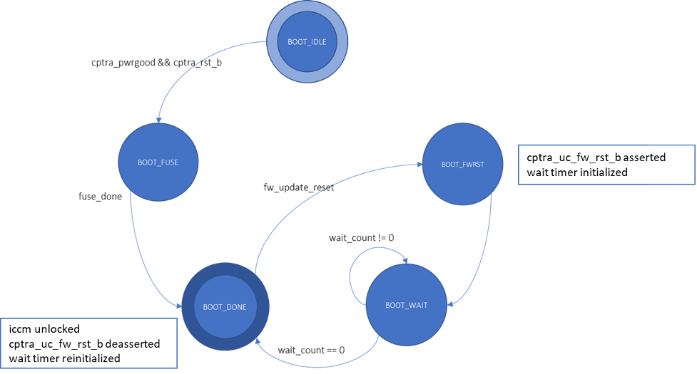
Impactless firmware updates may be initiated by writing to the fw_update_reset register after Caliptra comes out of global reset and enters the BOOT_DONE state. In the BOOT_FWRST state, only the reset to the RISC-V core is asserted and the wait timer is initialized. After the timer expires, the FSM advances from the BOOT_WAIT to BOOT_DONE state where the reset is deasserted and ICCM is unlocked.
RISC-V core
The RISC-V core is VeeR EL2 from CHIPS Alliance. It is a 32-bit CPU core that contains a 4-stage, scalar, in-order pipeline. The core supports RISC-V’s integer(I), compressed instruction(C), multiplication and division (M), instruction-fetch fence, CSR, and subset of bit manipulation instructions (Z) extensions. A link to the RISC-V VeeR EL2 Programmer’s Reference Manual is provided in the References section.
Configuration
The RISC-V core is highly configurable and has the following settings.
| Parameter | Configuration |
|---|---|
| Interface | AHB-Lite |
| DCCM | 128 KiB |
| ICCM | 128 KiB |
| I-Cache | Disabled |
| Reset Vector | 0x00000000 |
| Fast Interrupt Redirect | Enabled |
| External Interrupts | 31 |
Embedded memory export
Internal RISC-V SRAM memory components are exported from the Caliptra subsystem to support adaptation to various fabrication processes. For more information, see the Caliptra Integration Specification.
Memory map address regions
The 32-bit address region is subdivided into 16 fixed-sized, contiguous 256 MB regions. The following table describes the address mapping for each of the AHB devices that the RISC-V core interfaces with.
| Subsystem | Address size | Start address | End address |
|---|---|---|---|
| ROM | 48 KiB | 0x0000_0000 | 0x0000_BFFF |
| Cryptographic | 512 KiB | 0x1000_0000 | 0x1007_FFFF |
| Peripherals | 32 KiB | 0x2000_0000 | 0x2000_7FFF |
| SoC IFC | 256 KiB | 0x3000_0000 | 0x3003_FFFF |
| RISC-V Core ICCM | 128 KiB | 0x4000_0000 | 0x4001_FFFF |
| RISC-V Core DCCM | 128 KiB | 0x5000_0000 | 0x5001_FFFF |
| RISC-V MM CSR (PIC) | 256 MiB | 0x6000_0000 | 0x6FFF_FFFF |
Cryptographic subsystem
The following table shows the memory map address ranges for each of the IP blocks in the cryptographic subsystem.
| IP/Peripheral | Target # | Address size | Start address | End address |
|---|---|---|---|---|
| Cryptographic Initialization Engine | 0 | 32 KiB | 0x1000_0000 | 0x1000_7FFF |
| ECC Secp384 | 1 | 32 KiB | 0x1000_8000 | 0x1000_FFFF |
| HMAC384 | 2 | 4 KiB | 0x1001_0000 | 0x1001_0FFF |
| Key Vault | 3 | 8 KiB | 0x1001_8000 | 0x1001_9FFF |
| PCR Vault | 4 | 8 KiB | 0x1001_A000 | 0x1001_BFFF |
| Data Vault | 5 | 8 KiB | 0x1001_C000 | 0x1001_DFFF |
| SHA512 | 6 | 32 KiB | 0x1002_0000 | 0x1002_7FFF |
| SHA256 | 13 | 32 KiB | 0x1002_8000 | 0x1002_FFFF |
Peripherals subsystem
The following table shows the memory map address ranges for each of the IP blocks in the peripherals’ subsystem.
| IP/Peripheral | Target # | Address size | Start address | End address |
|---|---|---|---|---|
| QSPI | 7 | 4 KiB | 0x2000_0000 | 0x2000_0FFF |
| UART | 8 | 4 KiB | 0x2000_1000 | 0x2000_1FFF |
| CSRNG | 15 | 4 KiB | 0x2000_2000 | 0x2000_2FFF |
| ENTROPY SRC | 16 | 4 KiB | 0x2000_3000 | 0x2000_3FFF |
SoC interface subsystem
The following table shows the memory map address ranges for each of the IP blocks in the SoC interface subsystem.
| IP/Peripheral | Target # | Address size | Start address | End address |
|---|---|---|---|---|
| Mailbox SRAM Direct Access | 10 | 128 KiB | 0x3000_0000 | 0x3001_FFFF |
| Mailbox CSR | 10 | 4 KiB | 0x3002_0000 | 0x3002_0FFF |
| SHA512 Accelerator CSR | 10 | 4 KiB | 0x3002_1000 | 0x3002_1FFF |
| Mailbox | 10 | 64 KiB | 0x3003_0000 | 0x3003_FFFF |
RISC-V core local memory blocks
The following table shows the memory map address ranges for each of the local memory blocks that interface with RISC-V core.
| IP/Peripheral | Target # | Address size | Start address | End address |
|---|---|---|---|---|
| ICCM0 (via DMA) | 12 | 128 KiB | 0x4000_0000 | 0x4001_FFFF |
| DCCM | 11 | 128 KiB | 0x5000_0000 | 0x5001_FFFF |
Interrupts
The VeeR-EL2 processor supports multiple types of interrupts, including non-maskable interrupts (NMI), software interrupts, timer interrupts, external interrupts, and local interrupts. Local interrupts are events not specified by the RISC-V standard, such as auxiliary timers and correctable errors.
Caliptra uses NMI in conjunction with a watchdog timer to support fatal error recovery and system restart. For more information, see the Watchdog timer section.
Software and local interrupts are not implemented in the first generation of Caliptra. Standard RISC-V timer interrupts are implemented using the mtime and mtimecmp registers defined in the RISC-V Privileged Architecture Specification. Both mtime and mtimecmp are included in the soc_ifc register bank, and are accessible by the internal microprocessor to facilitate precise timing tasks. Frequency for the timers is configured by the SoC using the dedicated timer configuration register, which satisfies the requirement prescribed in the RISC-V specification for such a mechanism. These timer registers drive the timer_int pin into the internal microprocessor.
Non-maskable interrupts
Caliptra's RISC-V processor has access to an internal register that allows configuration of the NMI vector. When an NMI occurs, the program counter jumps to the address indicated by the contents of this register. For more information, see NMI Vector.
External interrupts
Caliptra uses the external interrupt feature to support event notification from all attached peripheral components in the subsystem. The RISC-V processor supports multiple priority levels (ranging from 1-15), which allows firmware to configure interrupt priority per component.
Errors and notifications are allocated as interrupt events for each component, with error interrupts assigned a higher priority and expected to be infrequent.
Notification interrupts are used to alert the processor of normal operation activity, such as completion of requested operations or arrival of SoC requests through the shared interface.
Vector 0 is reserved by the RISC-V processor and may not be used, so vector assignment begins with Vector 1. Bit 0 of the interrupt port to the processor corresponds with Vector 1. The following table shows assignment of interrupt vectors to the corresponding IP block. The illustrated interrupt priority assignment is only an example, and does not correspond with actual priorities assigned in the final Caliptra firmware. These interrupt priorities are used in the validation firmware that tests the RTL, and are defined in caliptra_defines.h.
| IP/Peripheral | Interrupt vector | Interrupt priority example (Increasing, Max 15) |
|---|---|---|
| Cryptographic Initialization Engine (Errors) | 1 | 8 |
| Cryptographic Initialization Engine (Notifications) | 2 | 7 |
| ECC (Errors) | 3 | 8 |
| ECC (Notifications) | 4 | 7 |
| HMAC (Errors) | 5 | 8 |
| HMAC (Notifications) | 6 | 7 |
| Key Vault (Errors) | 7 | 8 |
| Key Vault (Notifications) | 8 | 7 |
| SHA512 (Errors) | 9 | 8 |
| SHA512 (Notifications) | 10 | 7 |
| SHA256 (Errors) | 11 | 8 |
| SHA256 (Notifications) | 12 | 7 |
| QSPI (Errors) | 13 | 4 |
| QSPI (Notifications) | 14 | 3 |
| UART (Errors) | 15 | 4 |
| UART (Notifications) | 16 | 3 |
| RESERVED | 17 | 4 |
| RESERVED | 18 | 3 |
| Mailbox (Errors) | 19 | 8 |
| Mailbox (Notifications) | 20 | 7 |
Watchdog timer
The primary function of Caliptra Watchdog Timer (WDT) is to reset the microcontroller (Caliptra), in the event of a software malfunction, by resetting the device if it has not been cleared in software. It is a two-stage timer, independent of the RISCV core.
Operation
The WDT consists of two timers. When enabled in cascade mode (done by enabling Timer 1 alone), the WDT increments Timer 1 until the counter rolls over or times out. Typically, the timer is serviced at regular intervals to prevent it from overflowing or rolling over. If Timer 1 has not timed out, Timer 2 is disabled and held at its initial value. However, when Timer 1 does roll over, it triggers an error interrupt to the RISC-V core. In parallel, Timer 2 is enabled and begins counting. If the interrupt is serviced before Timer 2 times out, the timers are reset and continue to operate normally. If Timer 2 times out, it asserts an SoC fatal error and an NMI. The SoC fatal error is also captured in the CPTRA_HW_ERROR_FATAL register, which can be cleared by the SoC by writing a 1. A warm reset is required by the SoC to reset the timers when Timer 2 times out.
The WDT timers can be configured to operate independent of each other. When the enable register for Timer 2 is set, the default configuration of cascaded timers is disabled and both timers count independently of each other. In this case, a timeout on Timer 2 causes an error interrupt to the RISC-V core similar to Timer 1. Disabling Timer 2 configures the timers back into the default cascaded mode.
Each timer has an enable bit, a restart bit, and a 64-bit timeout value register that can be programmed as needed. The restart bit is used to service the timers and restart counting. The timeout period registers can be configured to the desired upper bound of timers.
If the WDT timers are disabled and then re-enabled with a new timeout period, they must be restarted by setting the appropriate control register (restart bit). If the timers are temporarily disabled and re-enabled with the same timeout period, they resume counting and do not restart from 0.
For more details regarding the register interface to control the WDT, see the register documentation published in the RTL GitHub repository.
The following figure shows the two timers.
Figure 3: Caliptra Watchdog Timer
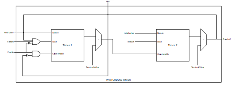
Prescale settings
Assuming a clock source of 500 MHz, a timeout value of 32’hFFFF_FFFF results in a timeout period of ~8.5 seconds. Two 32-bit registers are provided for each timer, allowing a 64-bit timeout period to be programmed for each timer. This accommodates a maximum timeout value of over 1000 years for the same 500 Mhz clock source.
Microcontroller interface
The Caliptra microcontroller communicates with the mailbox through its internal AHB-Lite fabric.
AHB-lite interface
AHB-lite is a subset of the full AHB specification. It is primarily used in single initiator systems. This interface connects VeeR EL2 Core (LSU initiator) to the target devices. See Caliptra Core for information.
The interface can be customized to support variable address and data widths, and a variable number of target devices. Each target device is assigned an address range within the 32-bit address memory map region. The interface includes address decoding logic to route data to the appropriate AHB target device based on the address specified.
The integration parameters for Caliptra’s AHB-lite interface are shown in the following table.
| Parameter | Value |
|---|---|
| ADDRESS_WIDTH | 32 |
| DATA_WIDTH | 64 |
| NUM_OF_SLAVES | 17 |
Each IP component in the Caliptra system uses a native AHB data width of 32-bits (1 dword). The AHB responder logic in each IP component contains width conversion logic that transforms from the fabric data width of 64-bits to this native 32-bit width. The conversion involves calculating the dword offset (either 0 or 1) relative to the native 64-bit width by evaluating bit [2] of the address line. This information is used to extract the correct 32-bits from the native write data line. If there is a data offset, data is shifted down by 32-bits; otherwise, the upper 32-bits are simply truncated. This new dword-address is passed to the internal register interface along with the dword-sized data. A similar conversion works in reverse to correctly place read data in the response data line from the responder.
As a result of this implementation, 64-bit data transfers are not supported on the Caliptra AHB fabric. Firmware running on the internal microprocessor may only access memory and registers using a 32-bit or smaller request size, as 64-bit transfer requests will be corrupted.
Cryptographic subsystem
For details, see the Cryptographic subsystem architecture section.
Peripherals subsystem
Caliptra includes QSPI and UART peripherals that are used to facilitate alternative operating modes and debug. In the first generation, Caliptra does not support enabling the QSPI interface. Similarly, the UART interface exists to facilitate firmware debug in an FPGA prototype, but should be disabled in final silicon. SystemVerilog defines used to disable these peripherals are described in the Caliptra Integration Specification. Operation of these peripherals is described in the following sections.
QSPI Flash Controller
Caliptra implements a QSPI block that can communicate with 2 QSPI devices. This QSPI block is accessible to FW over the AHB-lite Interface.
The QSPI block is composed of the spi_host implementation. For information, see the SPI_HOST HWIP Technical Specification. The core code (see spi_host) is reused but the interface to the module is changed to AHB-lite and the number of chip select lines supported is increased to 2. The design provides support for Standard SPI, Dual SPI, or Quad SPI commands. The following figure shows the QSPI flash controller.
Figure 4: QSPI flash controller
Operation
Transactions flow through the QSPI block starting with AHB-lite writes to the TXDATA FIFO. Commands are then written and processed by the control FSM, orchestrating transmissions from the TXDATA FIFO and receiving data into the RXDATA FIFO.
The structure of a command depends on the device and the command itself. In the case of a standard SPI device, the host IP always transmits data on qspi_d_io[0] and always receives data from the target device on qspi_d_io[1]. In Dual or Quad modes, all data lines are bi-directional, thus allowing full bandwidth in transferring data across 4 data lines.
A typical SPI command consists of different segments that are combined as shown in the following example. Each segment can configure the length, speed, and direction. As an example, the following SPI read transaction consists of 2 segments.
Figure 5: SPI read transaction segments
| Segment # | Length (Bytes) | Speed | Direction | TXDATA FIFO | RXDATA FIFO |
|---|---|---|---|---|---|
| 1 | 4 | standard | TX qspi_d_io[0] | [0] 0x3 (ReadData) [1] Addr[23:16] [2] Addr[15:8] [3] Addr[7:0] | |
| 2 | 1 | standard | RX qspi_d_io[1] | [0] Data [7:0] |
In this example, the ReadData (0x3) command was written to the TXDATA FIFO, followed by the 3B address. This maps to a total of 4 bytes that are transmitted out across qspi_d_io[0] in the first segment. The second segment consists of a read command that receives 1 byte of data from the target device across qspi_d_io[1].
QSPI consists of up to four command segments in which the host:
- Transmits instructions or data at the standard rate
- Transmits instructions address or data on 2 or 4 data lines
- Holds the bus in a high-impedance state for some number of dummy cycles where neither side transmits
- Receives information from the target device at the specified rate (derived from the original command)
The following example shows the QSPI segments.
Figure 6: QSPI segments
| Segment # | Length (Bytes) | Speed | Direction | TXDATA FIFO | RXDATA FIFO |
|---|---|---|---|---|---|
| 1 | 1 | standard | TX qspi_d_io[3:0] | [0] 0x6B (ReadDataQuad) | |
| 2 | 3* | quad | TX qspi_d_io[3:0] | [1] Addr[23:16] [2] Addr[15:8] [3] Addr[7:0] | |
| 3 | 2 | N/A | None (Dummy) | ||
| 4 | 1 | quad | RX qspi_d_io[3:0] | [0] Data[7:0] |
Note: In the preceding figure, segment 2 doesn’t show bytes 2 and 3 for brevity.
Configuration
The CONFIGOPTS multi-register has one entry per CSB line and holds clock configuration and timing settings that are specific to each peripheral. After the CONFIGOPTS multi-register is programmed for each SPI peripheral device, the values can be left unchanged.
The most common differences between target devices are the requirements for a specific SPI clock phase or polarity, CPOL and CPHA. These clock parameters can be set via the CONFIGOPTS.CPOL or CONFIGOPTS.CPHA register fields.
The SPI clock rate depends on the peripheral clock and a 16b clock divider configured by CONFIGOPTS.CLKDIV. The following equation is used to configure the SPI clock period:

By default, CLKDIV is set to 0, which means that the maximum frequency that can be achieved is at most half the frequency of the peripheral clock (Fsck = Fclk/2).
We can rearrange the equation to solve for the CLKDIV:

Assuming a 400MHz target peripheral, and a SPI clock target of 100MHz:
CONFIGOPTS.CLKDIV = (400/(2*100)) -1 = 1
The following figure shows CONFIGOPTS.
Figure 7: CONFIGOPTS
Signal descriptions
The QSPI block architecture inputs and outputs are described in the following table.
| Name | Input or output | Description |
|---|---|---|
| clk_i | input | All signal timings are related to the rising edge of clk. |
| rst_ni | input | The reset signal is active LOW and resets the core. |
| cio_sck_o | output | SPI clock |
| cio_sck_en_o | output | SPI clock enable |
| cio_csb_o[1:0] | output | Chip select # (one hot, active low) |
| cio_csb_en_o[1:0] | output | Chip select # enable (one hot, active low) |
| cio_csb_sd_o[3:0] | output | SPI data output |
| cio_csb_sd_en_o | output | SPI data output enable |
| cio_csb_sd_i[3:0] | input | SPI data input |
SPI_HOST IP programming guide
The operation of the SPI_HOST IP proceeds in seven general steps.
To initialize the IP:
- Program the CONFIGOPTS multi-register with the appropriate timing and polarity settings for each csb line.
- Set the desired interrupt parameters.
- Enable the IP.
Then for each command:
-
Load the data to be transmitted into the FIFO using the TXDATA memory window.
-
Specify the target device by programming the CSID.
-
Specify the structure of the command by writing each segment into the COMMAND register.
For multi-segment transactions, assert COMMAND.CSAAT for all but the last command segment.
-
For transactions that expect to receive a reply, the data can then be read back from the RXDATA window.
Steps 4-7 are then repeated for each subsequent command.
UART
Caliptra implements a UART block that can communicate with a serial device that is accessible to FW over the AHB-lite Interface. This is a configuration that the SoC opts-in by defining CALIPTRA_INTERNAL_UART.
The UART block is composed of the uart implementation. For information, see the UART HWIP Technical Specification. The design provides support for a programmable baud rate. The UART block is shown in the following figure.
Figure 8: UART block
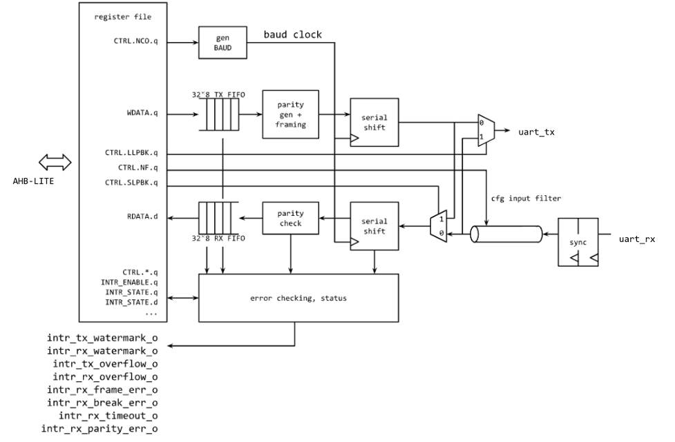
Operation
Transactions flow through the UART block starting with an AHB-lite write to WDATA, which triggers the transmit module to start a UART TX serial data transfer. The TX module dequeues the byte from the internal FIFO and shifts it out bit by bit at the baud rate. If TX is not enabled, the output is set high and WDATA in the FIFO is queued up.
The following figure shows the transmit data on the serial lane, starting with the START bit, which is indicated by a high to low transition, followed by the 8 bits of data.
Figure 9: Serial transmission frame
![]()
On the receive side, after the START bit is detected, the data is sampled at the center of each data bit and stored into a FIFO. A user can monitor the FIFO status and read the data out of RDATA.
Configuration
The baud rate can be configured using the CTRL.NCO register field. This should be set using the following equation:

If the desired baud rate is 115,200bps:


Signal descriptions
The UART block architecture inputs and outputs are described in the following table.
| Name | Input or output | Description |
|---|---|---|
| clk_i | input | All signal timings are related to the rising edge of clk. |
| rst_ni | input | The reset signal is active LOW and resets the core. |
| cio_rx_i | input | Serial receive bit |
| cio_tx_o | output | Serial transmit bit |
SoC mailbox
For more information on the mailbox protocol, see Mailbox in the Caliptra Integration Specification. Mailbox registers accessible to the Caliptra microcontroller are defined in internal-regs/mbox_csr.
Security state
Caliptra uses the MSB of the security state input to determine whether or not Caliptra is in debug mode.
When Caliptra is in debug mode:
-
Security state MSB is set to 0.
-
Caliptra JTAG is opened for the microcontroller and HW debug.
-
Device secrets (UDS, FE, key vault, and obfuscation key) are programmed to debug values.
If a transition to debug mode happens during ROM operation, any values computed from the use of device secrets may not match expected values.
Transitions to debug mode trigger a hardware clear of all device secrets, and also trigger an interrupt to FW to inform of the transition. FW is responsible for initiating another hardware clear of device secrets utilizing the clear secrets register, in case any derivations were in progress and stored after the transition was detected. FW may open the JTAG after all secrets are cleared.
Debug mode values may be set by integrators in the Caliptra configuration files. The default values are shown in the following table.
| Name | Default value |
|---|---|
| Obfuscation Key Debug Value | All 0x1 |
| UDS Debug Value | All 0x1 |
| Field Entropy Debug Value | All 0x1 |
| Key Vault Debug Value 0 | All 0xA |
| Key Vault Debug Value 1 | All 0x5 |
Clock gating
Caliptra provides a clock gating feature that turns off clocks when the microcontroller is halted. Clock gating is disabled by default, but can be globally enabled via the following register.
| Control register | Start address | Description |
|---|---|---|
| CPTRA_CLK_GATING_EN | 0x300300bc | Register bit to enable or disable the clock gating feature. |
When enabled, halting the microcontroller turns off clocks to all of the cryptographic subsystem, the vaults (key vault, PCR vault, and data vault), mailbox SRAM, SoC interface, and peripherals subsystem. The Watchdog timer and SoC registers run on the gated RDC clock. The RV core implements its own clock gating mechanism. Halting the core automatically turns off its clock.
There are a total of 4 clocks in Caliptra: ungated clock, gated clock, gated RDC clock, and gated SoC IFC clock. The following table shows the different modules and their designated clocks.
| Module | Clock |
|---|---|
| RV core | Clk |
| SOC IFC | Clk; clk_cg; rdc_clk_cg; soc_ifc_clk_cg |
| Crypto subsystem | Clk_cg |
| Vaults | Clk_cg |
| Peripherals subsystem | Clk_cg |
| AHB Lite IF, 2to1 Mux | Clk_cg |
| TRNG | Clk_cg |
Wake up conditions
For details on halting the core and waking up the core from the halt state, see section 5 of the RISC-V VeeR EL2 Programmer's Reference Manual.
When the RV core wakes up, all clocks are enabled. However, when the core is halted, it is possible to wake up Caliptra clocks through:
-
A change in generic_input_wires
-
Cptra_fatal_error assertion
-
Entry to debug or scan modes
-
JTAG accesses
-
APB transactions
Activity on the APB interface only wakes up the SoC IFC clock. All other clocks remain off until any other condition is met or the core exits the halt state.
| Cpu_halt_status | PSEL | Generic input wires || fatal error || debug/scan mode ||JTAG access | Expected behavior |
|---|---|---|---|
| 0 | X | X | All gated clocks active |
| 1 | 0 | 0 | All gated clocks inactive |
| 1 | 0 | 1 | All gated clocks active (as long as condition is true) |
| 1 | 1 | 0 | Soc_ifc_clk_cg active (as long as PSEL = 1) All other clks inactive |
| 1 | 1 | 1 | Soc_ifc_clk_cg active (as long as condition is true OR PSEL = 1) All other clks active (as long as condition is true) |
Usage
The following applies to the clock gating feature:
- The core should only be halted after all pending vault writes are done and cryptographic operations are complete.
- While the core is halted, any APB transaction wakes up the SoC interface clock and leaves all other clocks disabled. If the core is still halted when the APB transactions are done, the SoC interface clock is returned to a disabled state. .
- The RDC clock is similar to an ungated clock and is only disabled when a reset event occurs. This avoids metastability on flops. The RDC clock operates independently of core halt status.
Timing information
The following figure shows the timing information for clock gating.
Figure 10: Clock gating timing
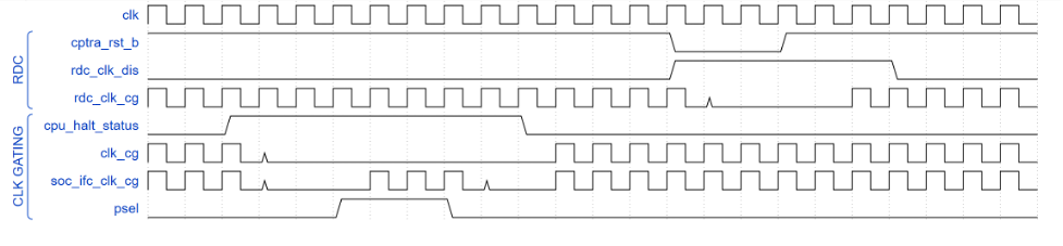
Integrated TRNG
Caliptra implements a true random number generator (TRNG) block for local use models. Firmware is able to read a random number from the TRNG core by accessing its register block over the AHB-lite interface. This is a configuration that SoC integrators enable by defining CALIPTRA_INTERNAL_TRNG.
This TRNG block is a combination of entropy source and CSRNG implementations. For information, see the ENTROPY_SRC HWIP Technical Specification and the CSRNG HWIP Technical Specification. The core code (see entropy source and csrng) is reused from here but the interface to the module is changed to AHB-lite. This design provides an interface to an external physical random noise generator. This is also referred to as a physical true random number generator (PTRNG). The PTRNG external source is a physical true random noise source. A noise source and its relation to an entropy source are defined by SP 800-90B.
The block is instantiated based on a design parameter chosen at integration time. This is to provide options for SoC to reuse an existing TRNG to build an optimized SoC design. For the optimized scenarios, SoC needs to follow the External-TRNG REQ HW API.
The following figure shows the integrated TRNG block.
Figure 11: Integrated TRNG block
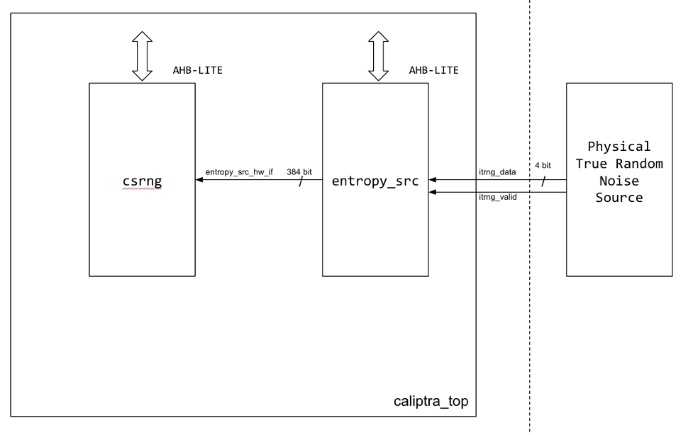
The following figure shows the CSRNG block.
Figure 12: CSRNG block
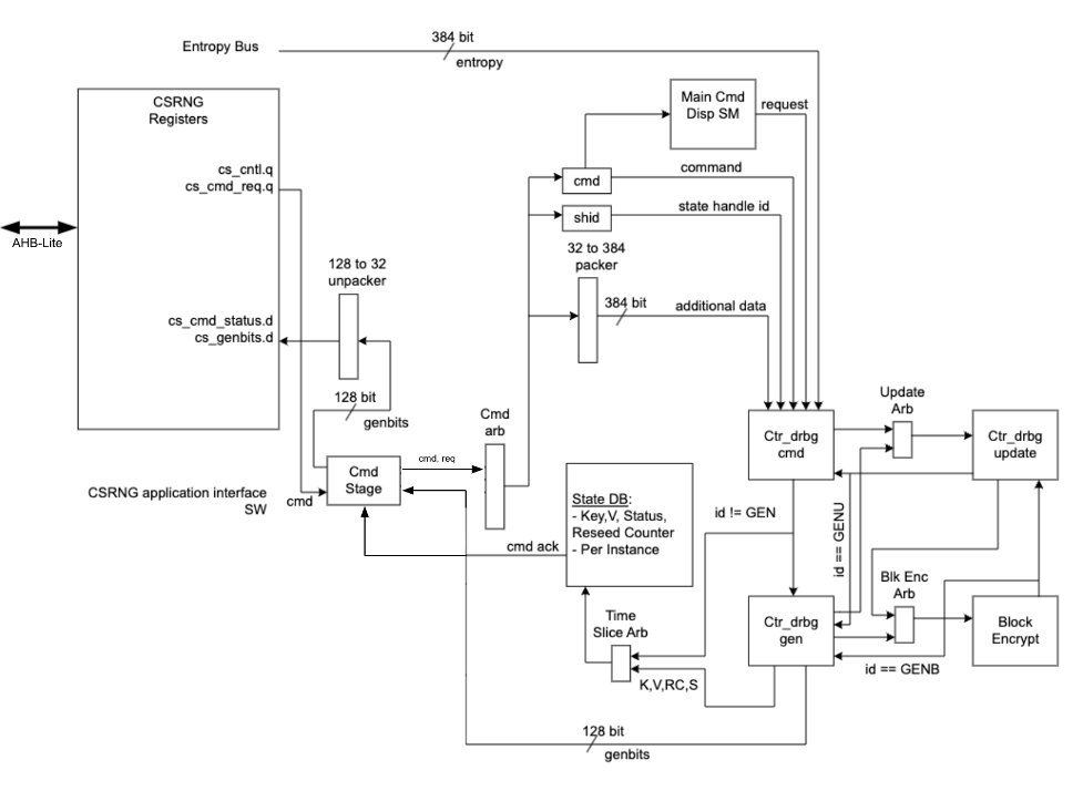
The following figure shows the entropy source block.
Figure 13: Entropy source block
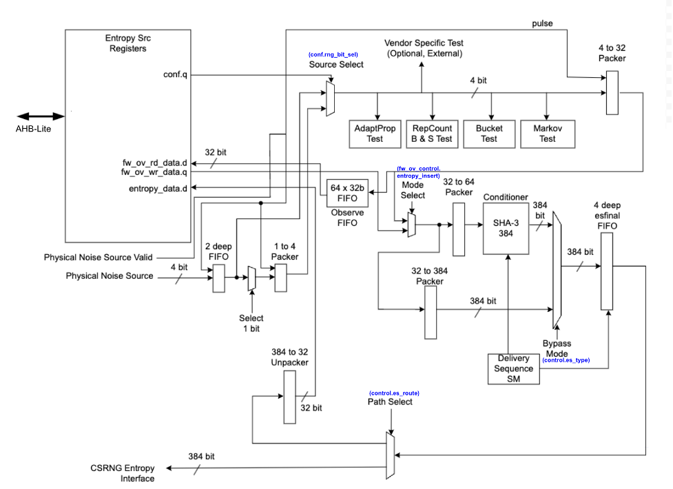
Operation
Requests for entropy bits start with command requests over the AHB-lite interface to the csrng CMD_REQ register.
The following describes the fields of the command request header:
-
Application Command: Selects one of five operations to perform. The commands supported are instantiate, reseed, generate, update, and uninstantiate.
-
Command Length: Number of 32-bit words that can optionally be appended to the command. A value of zero will only transfer the command header. A value of 4'hc transfers the header plus an additional twelve 32-bit words of data.
-
Command Flag0: flag0 is associated with the current command. Setting this field to True (4’h6) enables flag0 to be enabled. Note that flag0 is used for the instantiate and reseed commands only; for all other commands, the flag0 value is ignored.
-
Generate Length: Only defined for the generate command, this field is the total number of cryptographic entropy blocks requested. Each unit represents 128 bits of entropy returned. A value of 8 would return a total of 1024 bits. The maximum size supported is 4096.
First an instantiate command is requested over the SW application interface to initialize an instance in the CSRNG module. Depending on the flag0 and clen fields in the command header, a request to the entropy_src module over the entropy interface is sent to seed the csrng. This can take a few milliseconds if the seed entropy is not immediately available.
Example instantiation:
acmd = 0x1 (Instantiate)
clen/flag0 = The seed behavior is described in the following table.
glen = Not used
| flag0 | clen | Description |
|---|---|---|
| F | 0 | Only entropy source seed is used. |
| F | 1-12 | Entropy source seed is xor'ed with provided additional data. |
| T | 0 | Seed of zero is used (no entropy source seed used). |
| T | 1-12 | Only provided additional data is used as seed. |
Next a generate command is used to request generation of cryptographic entropy bits. The glen field defines how many 128 bit words are to be returned to the application interface. After the generated bits are ready, they can be read out via the GENBITS register. This register must be read out glen * 4 times for each request made.
Example generate command:
acmd = 0x3 (Generate)
clen = 0
flag0 = false (4’h9)
glen = 4 (4 *128 = 512b)
This requires 16 reads from GENBITS to read out all of the generated entropy.
Configuration
The HW application interfaces are not supported. Only the SW application interface should be used for this design.
Physical true random noise source signal descriptions
These are the top level signals defined in caliptra_top.
| Name | Input or output | Description |
|---|---|---|
| itrng_data | input | Physical true random noise source data |
| itrng_valid | input | Valid is asserted high for one cycle when data is valid. The expected valid output rate is about 50KHz. |
The following figure shows the top level signals defined in caliptra_top.
Figure 14: caliptra_top signals
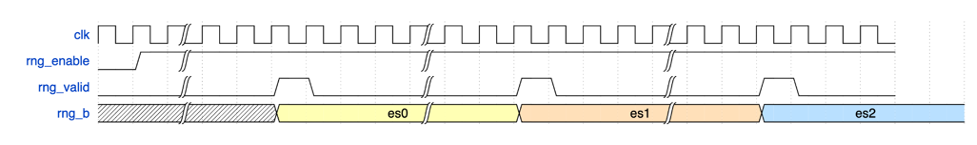
Entropy source signal descriptions
The following table provides descriptions of the entropy source signals.
| Name | Input or output | Description |
|---|---|---|
| clk_i | input | All signal timings are related to the rising edge of clk. |
| rst_ni | input | The reset signal is active LOW and resets the core. |
| entropy_src_rng_req | output | Request from the entropy_src module to the physical true random noise source to start generating data. |
| entropy_src_rng_rsp | input | Contains the internal TRNG data and a flag indicating the data is valid. Valid is asserted high for one cycle when data is valid. |
| entropy_src_hw_if_i | input | Downstream block request for entropy bits. |
| entropy_src_hw_if_o | output | 384 bits of entropy data. Valid when es_ack is asserted high. |
| cs_aes_halt_i | input | Response from csrng that all requests to AES block are halted. |
| cs_aes_halt_o | output | Request to csrng to halt requests to the AES block for power leveling purposes. |
The following figure shows the entropy source signals.
Figure 15: Entropy source signals
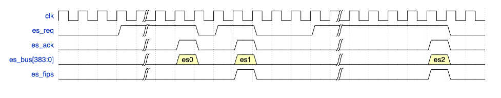
CSRNG signal descriptions
The following table provides descriptions for the CSRNG signals.
| Name | Input or output | Description |
|---|---|---|
| clk_i | input | All signal timings are related to the rising edge of clk. |
| rst_ni | input | The reset signal is active LOW and resets the core. |
| otp_en_csrng_sw_app_read_i | input | Enable firmware to access the ctr_drbg internal state and genbits through registers. |
| lc_hw_debug_en_i | input | Lifecycle that selects which diversification value is used for xoring with the seed from entropy_src. |
| entropy_src_hw_if_i | input | 384 bits of entropy data. Valid when es_ack is asserted high. |
| entropy_src_hw_if_o | output | Downstream block request for entropy bits. |
| cs_aes_halt_i | input | Request from entropy_src to halt requests to the AES block for power leveling purposes. |
| cs_aes_halt_o | output | Response to entropy_src that all requests to AES block are halted. |
The CSRNG may only be enabled if entropy_src is enabled. After it is disabled, CSRNG may only be re-enabled after entropy_src has been disabled and re-enabled.
External-TRNG REQ HW API
For SoCs that choose to not instantiate Caliptra’s integrated TRNG, Caliptra provides a TRNGREQ HW API.
- Caliptra asserts TRNG_REQ wire (FW made the request for a TRNG).
- SoC writes the TRNG architectural registers.
- SoC writes a done bit in the TRNG architectural registers.
- Caliptra desserts TRNG_REQ.
The reason to have a separate interface from the SoC mailbox is to ensure that this request is not intercepted by any SoC FW agents that communicate with the SoC mailbox. It is required for FIPS compliance that this TRNG HW API is always handled by a SoC HW gasket logic and not handled by SoC ROM/FW code.
SoC-SHA accelerator HW API
Caliptra provides a SHA accelerator HW API for SoC and Caliptra internal FW to use. It is atomic in nature in that only one of them can use the SHA accelerator HW API at the same time. Details of the SHA accelerator register block may be found in the GitHub repository in documentation generated from the register definition file.
Using the HW API:
- A user of the HW API first locks the accelerator by reading the LOCK register. A read that returns the value 0 indicates that the resource was locked for exclusive use by the requesting user. A write of ‘1 clears the lock.
- The USER register captures the APB pauser value of the requestor that locked the SHA accelerator. This is the only user that is allowed to control the SHA accelerator by performing APB register writes. Writes by any other agent on the APB interface are dropped.
- MODE register is written to set the SHA execution mode.
- SHA accelerator supports both SHA384 and SHA512 modes of operation.
- SHA supports streaming mode: SHA is computed on a stream of incoming data to the DATAIN register. The EXECUTE register, when set, indicates to the accelerator that streaming is complete. The accelerator can then publish the result into the DIGEST register. When the VALID bit of the STATUS register is set, then the result in the DIGEST register is valid.
- SHA supports Mailbox mode: SHA is computed on LENGTH (DLEN) bytes of data stored in the mailbox beginning at START_ADDRESS. This computation is performed when the EXECUTE register is set by the user. When the operation is completed and the result in the DIGEST register is valid, SHA accelerator sets the VALID bit of the STATUS register.
- The SHA computation engine in the SHA accelerator requires big endian data, but the SHA accelerator can accommodate mailbox input data in either the little endian or big endian format. By default, input data is assumed to be little endian and is swizzled to big endian at the byte level prior to computation. For the big endian format, data is loaded into the SHA engine as-is. Users may configure the SHA accelerator to treat data as big endian by setting the ENDIAN_TOGGLE bit appropriately.
- See the register definition for the encodings.
- SHA engine also provides a ‘zeroize’ function through its CONTROL register to clear any of the SHA internal state. This can be used when the user wants to conceal previous state for debug or security reasons.
JTAG implementation
For specific debug flows, see the JTAG/TAP Debug section in Caliptra: A Datacenter System on a Chip (SoC) Root of Trust (RoT).
The following figure shows the JTAG implementation within the Caliptra boundary. The output of the existing DMI wrapper is used to find the non-Core (Caliptra uncore) aperture to route the JTAG commands.
Caliptra’s JTAG/TAP should be implemented as a TAP EP. JTAG is open if the debug mode is set at the time of Caliptra reset deassertion.
Note: If the debug security state switches to debug mode anytime, the security assets and keys are still flushed even though JTAG is not open.
Figure 16: JTAG implementation
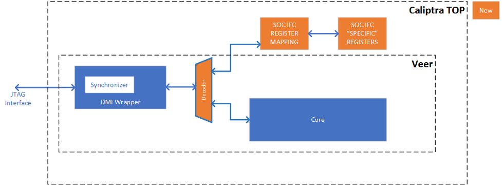
Cryptographic subsystem architecture
The architecture of Caliptra cryptographic subsystem includes the following components:
- Symmetric cryptographic primitives
- De-obfuscation engine
- SHA512/384 (based on NIST FIPS 180-4 [2])
- SHA256 (based on NIST FIPS 180-4 [2])
- HMAC384 (based on NIST FIPS 198-1 [5] and RFC 4868 [6])
- Public-key cryptography
- NIST Secp384r1 Deterministic Digital Signature Algorithm (based on FIPS-186-4 [11] and RFC 6979 [7])
- Key vault
- Key slots
- Key slot management
The high-level architecture of Caliptra cryptographic subsystem is shown in the following figure.
Figure 17: Caliptra cryptographic subsystem
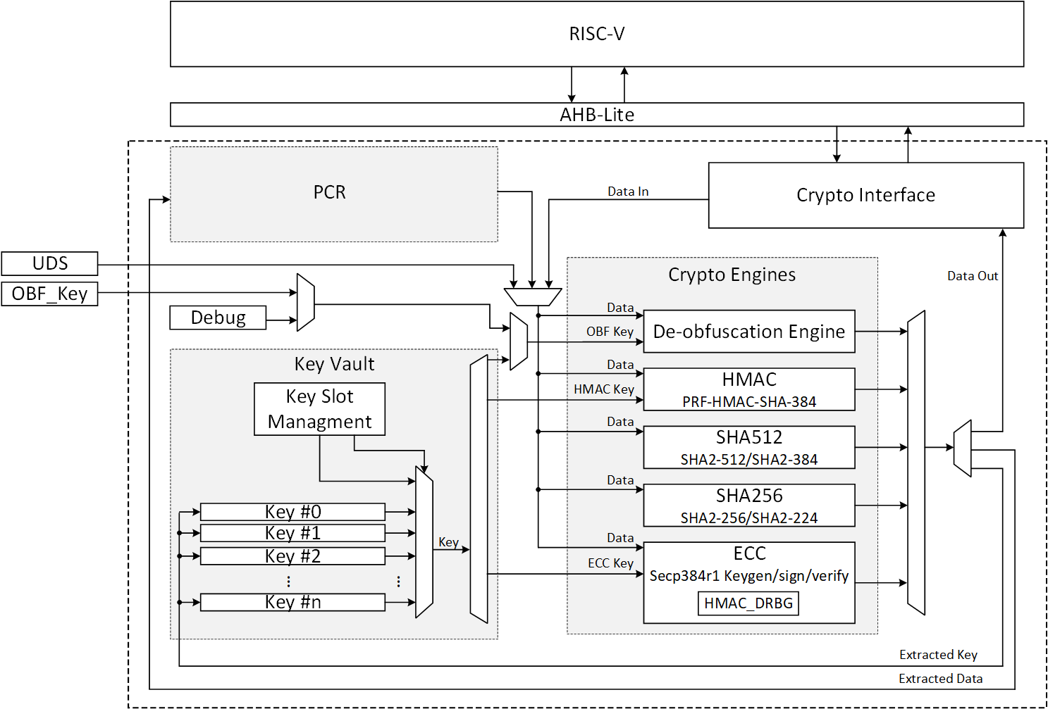
SHA512/SHA384
SHA512 is a function of cryptographic hash algorithm SHA-2. The hardware implementation is based on Secworks/SHA512 [1]. This implementation complies with the functionality in NIST FIPS 180-4 [2]. The implementation supports the SHA512 variants SHA-512/224, SHA-512/256, SHA384 and SHA512.
The SHA512 algorithm is described as follows:
- The message is padded by the host and broken into 1024-bit chunks
- For each chunk:
- The message is fed to the SHA512 core
- The core should be triggered by the host
- The SHA512 core status is changed to ready after hash processing
- The result digest can be read after feeding all message chunks
Operation
Padding
The message should be padded before feeding to the hash core. The input message is taken, and some padding bits are appended to it to get it to the desired length. The bits that are used for padding are simply ‘0’ bits with a leading ‘1’ (100000…000). The appended length of the message (before pre-processing), in bits, is a 128-bit big-endian integer.
The total size should be equal to 128 bits short of a multiple of 1024 since the goal is to have the formatted message size as a multiple of 1024 bits (N x 1024). The following figure shows the SHA512 input formatting.
Figure 18: SHA512 input formatting
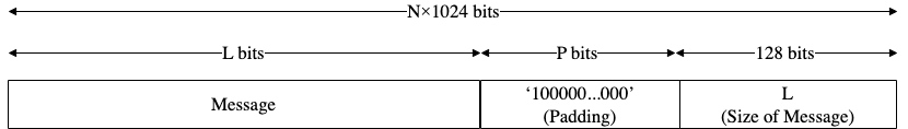
Hashing
The SHA512 core performs 80 iterative operations to process the hash value of the given message. The algorithm processes each block of 1024 bits from the message using the result from the previous block. For the first block, the initial vectors (IV) are used for starting the chain processing of each 1024-bit block.
FSM
The SHA512 architecture has the finite-state machine as shown in the following figure.
Figure 19: SHA512 FSM
Signal descriptions
The SHA512 architecture inputs and outputs are described in the following table.
| Name | Inputs and outputs | Description |
|---|---|---|
| clk | input | All signal timings are related to the rising edge of clk. |
| reset_n | input | The reset signal is active LOW and resets the core. This is the only active LOW signal. |
| init | input | The core is initialized and processes the first block of message. |
| next | input | The core processes the rest of the message blocks using the result from the previous blocks. |
| mode[1:0] | input | Indicates the hash type of the function. This can be: - SHA512/224 - SHA512/256 - SHA384 - SHA512 |
| zeroize | input | The core clears all internal registers to avoid any SCA information leakage. |
| block[1023:0] | input | The input padded block of message. |
| ready | output | When HIGH, the signal indicates the core is ready. |
| digest[511:0] | output | The hashed value of the given block. |
| digest_valid | output | When HIGH, the signal indicates that the result is ready. |
Address map
The SHA512 address map is shown here: sha512_reg — clp Reference (chipsalliance.github.io)
Pseudocode
The following pseudocode demonstrates how the SHA512 interface can be implemented.
Figure 20: SHA512 pseudocode
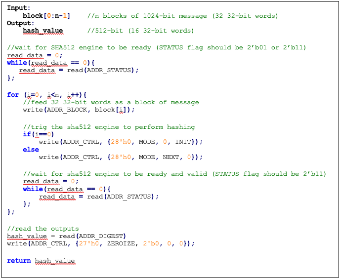
SCA countermeasure
We do not propose any countermeasure to protect the hash functions. Inherently, hash functions do not work like other cryptographic engines. Hash functions target integrity without requiring a secret key. Hence, the attacker can target only messages. Also, the attacker cannot build a CPA or DPA platform on the hash function because the same message ideally gives the same side-channel behavior.
If the attacker works on the multi-message mechanism, the attacker then needs to work with single trace attacks, which are very unlikely in ASIC/FPGA implementations. Also, our hash implementation is a noisy platform. As a result, we do not propose any SCA implementation countermeasure on the hash functions.
Performance
The SHA512 core performance is reported considering two different architectures: pure hardware architecture, and hardware/software architecture. These are described next.
Pure hardware architecture
In this architecture, the SHA512 interface and controller are implemented in hardware. The performance specification of the SHA512 architecture is shown in the following table.
| Operation | Cycle count [CCs] | Time [us] @ 400 MHz | Throughput [op/s] |
|---|---|---|---|
| Data_In transmission | 0.08 | ||
| Process | 87 | 0.22 | |
| Data_Out transmission | 16 | 0.04 | |
| Single block | 136 | 0.34 | 2,941,176 |
| Double block | 224 | 0.56 | 1,785,714 |
| 1 KiB message | 840 | 2.10 | 476,190 |
| 128 KiB message | 17,632 | 44.08 | 22,686 |
Hardware/software architecture
In this architecture, the SHA512 interface and controller are implemented in RISC-V core. The performance specification of the SHA512 architecture is shown in the following table.
| Operation | Cycle count [CCs] | Time [us]] @ 400 MHz | Throughput [op/s] |
|---|---|---|---|
| Data_In transmission | 990 | 2.48 | |
| Process | 139 | 0.35 | |
| Data_Out transmission | 387 | 0.97 | |
| Single block | 1,516 | 3.79 | 263,852 |
| Double block | 2,506 | 6.27 | 159,617 |
| 1 KiB message | 9,436 | 23.59 | 42,391 |
| 128 KiB message | 1,015,276 | 2,538.19 | 394 |
Pure software architecture
In this architecture, the SHA512 algorithm is implemented fully in software. The implementation is derived from the OpenSSL SHA512 implementation [3]. The performance numbers for this architecture are shown in the following table.
| Data size | Cycle count |
|---|---|
| 1 KiB | 147,002 |
| 4 KiB | 532,615 |
| 8 KiB | 1,046,727 |
| 12 KiB | 1,560,839 |
| 128 KiB | 16,470,055 |
SHA256
SHA256 is a function of the SHA-2 cryptographic hash algorithm. The hardware implementation is based on Secworks/SHA256 [1]. The implementation supports the two variants: SHA256/224 and SHA256.
The SHA256 algorithm is described as follows:
- The message is padded by the host and broken into 512-bit chunks
- For each chunk:
- The message is fed to the sha256 core
- The core should be triggered by the host
- The sha256 core status is changed to ready after hash processing
- The result digest can be read after feeding all message chunks
Operation
Padding
The message should be padded before feeding to the hash core. The input message is taken, and some padding bits are appended to the message to get it to the desired length. The bits that are used for padding are simply ‘0’ bits with a leading ‘1’ (100000…000). The appended length of the message (before pre-processing), in bits, is a 64-bit big-endian integer.
The total size should be equal to 64 bits, short of a multiple of 512 because the goal is to have the formatted message size as a multiple of 512 bits (N x 512).
The following figure shows SHA256 input formatting.
Figure 21: SHA256 input formatting

Hashing
The SHA256 core performs 64 iterative operations to process the hash value of the given message. The algorithm processes each block of 512 bits from the message using the result from the previous block. For the first block, the initial vectors (IV) are used to start the chain processing of each 512-bit block.
FSM
The SHA256 architecture has the finite-state machine as shown in the following figure.
Figure 22: SHA256 FSM
Signal descriptions
The SHA256 architecture inputs and outputs are described as follows.
| Name | Input or output | Description |
|---|---|---|
| clk | input | All signal timings are related to the rising edge of clk. |
| reset_n | input | The reset signal is active LOW and resets the core. This is the only active LOW signal. |
| init | input | The core is initialized and processes the first block of message. |
| next | input | The core processes the rest of the message blocks using the result from the previous blocks. |
| mode | input | Indicates the hash type of the function. This can be: - SHA256/224 - SHA256 |
| zeroize | input | The core clears all internal registers to avoid any SCA information leakage. |
| WNTZ_MODE* | input | SHA256 core is configured in Winternitz verification mode. |
| WNTZ_W[3:0]* | input | Winternitz W value. |
| WNTZ_N_MODE* | input | Winternitz n value(SHA192/SHA256 --> n = 24/32) |
| block[511:0] | input | The input padded block of message. |
| ready | output | When HIGH, the signal indicates the core is ready. |
| digest[255:0] | output | The hashed value of the given block. |
| digest_valid | output | When HIGH, the signal indicates the result is ready. |
* For more imformation about these inputs, please refer to LMS accelerator section.
Address map
The SHA256 address map is shown here: sha256_reg — clp Reference (chipsalliance.github.io).
Pseudocode
The following pseudocode demonstrates how the SHA256 interface can be implemented.
Figure 23: SHA256 pseudocode
SCA countermeasure
We do not propose any countermeasure to protect the hash functions. For more information, see SCA countermeasure in the SHA512/SHA384 section.
Performance
The SHA256 core performance is reported considering two different architectures: pure hardware architecture, and hardware/software architecture. These are described next.
Pure hardware architecture
In this architecture, the SHA256 interface and controller are implemented in hardware. The performance specification of the SHA256 architecture is reported as shown in the following table.
| Operation | Cycle count [CCs] | Time [us] @ 400 MHz | Throughput [op/s] |
|---|---|---|---|
| Data_In transmission | 17 | 0.04 | |
| Process | 66 | 0.17 | |
| Data_Out transmission | 8 | 0.02 | |
| Single block | 91 | 0.23 | 4,395,604 |
| Double block | 158 | 0.40 | 2,531,646 |
| 1 KiB message | 1163 | 2.91 | 343,938 |
Hardware/software architecture
In this architecture, the SHA256 interface and controller are implemented in RISC-V core. The performance specification of the SHA256 architecture is reported as shown in the following table.
| Operation | Cycle count [CCs] | Time [us] @ 400 MHz | Throughput [op/s] |
|---|---|---|---|
| Data_In transmission | 500 | 1.25 | |
| Process | 66 | 0.17 | |
| Data_Out transmission | 195 | 0.49 | |
| Single block | 761 | 1.90 | 525,624 |
| Double block | 1355 | 3.39 | 295,203 |
| 1 KiB message | 8761 | 21.90 | 45,657 |
HMAC384
Hash-based message authentication code (HMAC) is a cryptographic authentication technique that uses a hash function and a secret key. HMAC involves a cryptographic hash function and a secret cryptographic key. This implementation supports HMAC-SHA-384-192 as specified in NIST FIPS 198-1 [5]. The implementation is compatible with the HMAC-SHA-384-192 authentication and integrity functions defined in RFC 4868 [6].
Caliptra HMAC implementation uses SHA384 as the hash function, accepts a 384-bit key, and generates a 384-bit tag.
The implementation also supports PRF-HMAC-SHA-384. The PRF-HMAC-SHA-384 algorithm is identical to HMAC-SHA-384-192, except that variable-length keys are permitted, and the truncation step is not performed.
The HMAC algorithm is described as follows:
- The key is fed to the HMAC core to be padded
- The message is broken into 1024-bit chunks by the host
- For each chunk:
- The message is fed to the HMAC core
- The HMAC core should be triggered by the host
- The HMAC core status is changed to ready after hash processing
- The result digest can be read after feeding all message chunks
Operation
Padding
The message should be padded before feeding to the HMAC core. Internally, the i_padded key is concatenated with the message. The input message is taken, and some padding bits are appended to the message to get it to the desired length. The bits that are used for padding are simply ‘0’ bits with a leading ‘1’ (100000…000).
The total size should be equal to 128 bits, short of a multiple of 1024 because the goal is to have the formatted message size as a multiple of 1024 bits (N x 1024).
Figure 24: HMAC input formatting
The following figures show examples of input formatting for different message lengths.
Figure 25: Message length of 1023 bits

When the message is 1023 bits long, padding is given in the next block along with message size.
Figure 26: 1 bit padding

When the message size is 895 bits, a padding of ‘1’ is also considered valid, followed by the message size.
Figure 27: Multi block message

Messages with a length greater than 1024 bits are broken down into N 1024-bit blocks. The last block contains padding and the size of the message.
Hashing
The HMAC core performs the sha2-384 function to process the hash value of the given message. The algorithm processes each block of the 1024 bits from the message, using the result from the previous block. This data flow is shown in the following figure.
Figure 28: HMAC-SHA-384-192 data flow
FSM
The HMAC architecture has the finite-state machine as shown in the following figure.
Figure 29: HMAC FSM
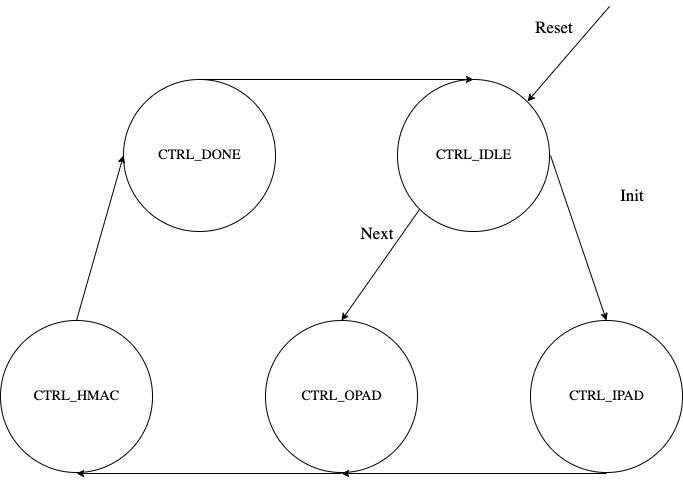
Signal descriptions
The HMAC architecture inputs and outputs are described in the following table.
| Name | Input or output | Description |
|---|---|---|
| clk | input | All signal timings are related to the rising edge of clk. |
| reset_n | input | The reset signal is active LOW and resets the core. This is the only active LOW signal. |
| init | input | The core is initialized and processes the key and the first block of the message. |
| next | input | The core processes the rest of the message blocks using the result from the previous blocks. |
| zeroize | input | The core clears all internal registers to avoid any SCA information leakage. |
| key[383:0] | input | The input key. |
| block[1023:0] | input | The input padded block of message. |
| LFSR_seed[159:0] | Input | The input to seed PRNG to enable the masking countermeasure for SCA protection. |
| ready | output | When HIGH, the signal indicates the core is ready. |
| tag[383:0] | output | The HMAC value of the given key or block. For PRF-HMAC-SHA-384, a 384-bit tag is required. For HMAC-SHA-384-192, the host is responsible for reading 192 bits from the MSB. |
| tag_valid | output | When HIGH, the signal indicates the result is ready. |
Address map
The HMAC address map is shown here: hmac_reg — clp Reference (chipsalliance.github.io).
Pseudocode
The following pseudocode demonstrates how the HMAC interface can be implemented.
Figure 30: HMAC pseudocode
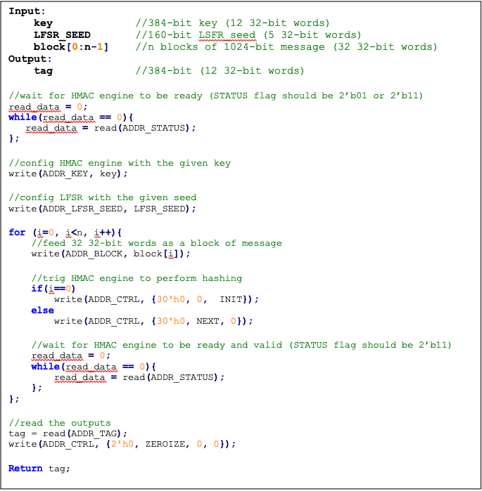
SCA countermeasure
In an attack model, an attacker can form hypotheses about the secret key value and compute the corresponding output values by using the Hamming Distance model as an appropriate leakage model. An attacker who has knowledge of the implementation for open-source architecture has an advantage. The attacker can capture the power consumption traces to verify their hypotheses, by partitioning the acquisitions or using Pearson’s correlation coefficient.
To protect the HMAC algorithm from side-channel attacks, a masking countermeasure is applied. This means that random values are added to the intermediate variables during the algorithm’s execution, so that the side-channel signals do not reveal any information about them.
The embedded countermeasures are based on "Differential Power Analysis of HMAC Based on SHA-2, and Countermeasures" by McEvoy et. al. To provide the required random values for masking intermediate values, a lightweight 74-bit LFSR is implemented. Based on “Spin Me Right Round Rotational Symmetry for FPGA-specific AES” by Wegener et. al., LFSR is sufficient for masking statistical randomness.
Each round of SHA512 execution needs 6,432 random bits, while one HMAC operation needs at least 4 rounds of SHA512 operations. However, the proposed architecture requires only 160-bit LFSR seed and provides first-order DPA attack protection at the cost of 10% latency overhead with negligible hardware resource overhead.
Performance
The HMAC core performance is reported considering two different architectures: pure hardware architecture, and hardware/software architecture. These are described next.
Pure hardware architecture
In this architecture, the HMAC interface and controller are implemented in hardware. The performance specification of the HMAC architecture is reported as shown in the following table.
| Operation | Cycle count [CCs] | Time [us] @ 400 MHz | Throughput [op/s] |
|---|---|---|---|
| Data_In transmission | 44 | 0.11 | - |
| Process | 254 | 0.635 | - |
| Data_Out transmission | 12 | 0.03 | - |
| Single block | 310 | 0.775 | 1,290,322 |
| Double block | 513 | 1.282 | 780,031 |
| 1 KiB message | 1,731 | 4.327 | 231,107 |
| 128 KiB message | 207,979 | 519.947 | 1,923 |
Hardware/software architecture
In this architecture, the HMAC interface and controller are implemented in RISC-V core. The performance specification of the HMAC architecture is reported as shown in the following table.
| Operation | Cycle count [CCs] | Time [us] @ 400 MHz | Throughput [op/s] |
|---|---|---|---|
| Data_In transmission | 1389 | 3.473 | - |
| Process | 253 | 0.633 | - |
| Data_Out transmission | 290 | 0.725 | - |
| Single block | 1932 | 4.83 | 207,039 |
| Double block | 3166 | 7.915 | 136,342 |
| 1 KiB message | 10,570 | 26.425 | 37,842 |
| 128 KiB message | 1,264,314 | 3,160.785 | 316 |
HMAC_DRBG
Hash-based message authentication code (HMAC) deterministic random bit generator (DRBG) is a cryptographic random bit generator that uses a HMAC function. HMAC_DRBG involves a cryptographic HMAC function and a seed. This architecture is designed as specified in section 10.1.2. of NIST SP 800-90A [12]. For ECC signing operation, the implementation is compatible with section 3.1. of RFC 6979 [7].
Caliptra HMAC_DRBG implementation uses HMAC384 as the HMAC function, accepts a 384-bit seed, and generates a 384-bit random value.
The HMAC algorithm is described as follows:
- The seed is fed to HMAC_DRBG core by the host
- For each 384-bit random value
- The core should be triggered by the host
- The HMAC_DRBG core status is changed to ready after HMAC processing
- The result digest can be read
Operation
HMAC_DRBG uses a loop of HMAC(K, V) to generate the random bits. In this algorithm, two constant values of K_init and V_init are used as follows:
        1. 	Set V_init = 0x01 0x01 0x01 ... 0x01  (V has 384-bit)
        2. 	Set K_init = 0x00 0x00 0x00 ... 0x00  (K has 384-bit)
        3. 	K_tmp = HMAC(K_init, V_init || 0x00 || entropy || nonce)
        4. 	V_tmp = HMAC(K_tmp,  V_init)
        5. 	K_new = HMAC(K_tmp,  V_tmp  || 0x01 || entropy || nonce)
        6. 	V_new = HMAC(K_new,  V_tmp)
        7. 	Set T = []
        8. 	T = T || HMAC(K_new, V_new)
        9. 	Return T if T is within the [1,q-1] range, otherwise:
        10.	K_new = HMAC(K_new,  V_new || 0x00)
        11.	V_new = HMAC(K_new,  V_new)
        12.	Jump to 8
For ECC KeyGen operation, HMAC_DRBG is used to generate privkey as follows:
Privkey = HMAC_DRBG(seed, nonce)
For ECC SIGNING operation, HMAC_DRBG is used to generate k as follows:
K = HMAC_DRBG(privkey, hashed_msg)
Signal descriptions
The HMAC_DRBG architecture inputs and outputs are described in the following table.
| Name | Input or output | Description |
|---|---|---|
| clk | input | All signal timings are related to the rising edge of clk. |
| reset_n | input | The reset signal is active LOW and resets the core. This is the only active LOW signal. |
| init | input | The core is initialized with the given seed and generates a 384-bit random value. |
| next | input | The core generates a new 384-bit random value using the result from the previous run. |
| zeroize | input | The core clears all internal registers to avoid any SCA information leakage. |
| entropy [383:0] | input | The input entropy. |
| nonce [383:0] | input | The input nonce. |
| LFSR_seed [147 :0] | input | The input to seed PRNG to enable masking countermeasure for SCA protection. |
| ready | output | When HIGH, the signal indicates the core is ready. |
| drbg [383:0] | output | The hmac_drbg value of the given inputs. |
| valid | output | When HIGH, the signal indicates the result is ready. |
Address map
The HMAC_DRBG is embedded into ECC architecture, since there is no address map to access it from FW.
SCA countermeasure
For information, see SCA countermeasure in the HMAC384 section.
ECC
The ECC unit includes the ECDSA (Elliptic Curve Digital Signature Algorithm) engine, offering a variant of the cryptographically secure Digital Signature Algorithm (DSA), which uses elliptic curve (ECC). A digital signature is an authentication method in which a public key pair and a digital certificate are used as a signature to verify the identity of a recipient or sender of information.
The hardware implementation supports deterministic ECDSA, 384 Bits (Prime Field), also known as NIST-Secp384r1, described in RFC6979.
Secp384r1 parameters are shown in the following figure.
Figure 31: Secp384r1 parameters
Operation
The ECDSA consists of three operations, shown in the following figure.
Figure 32: ECDSA operations
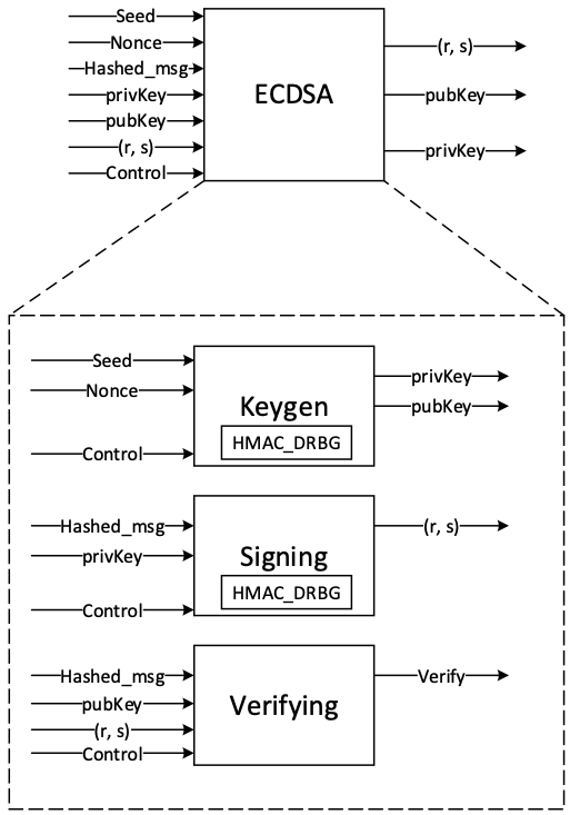
KeyGen
In the deterministic key generation, the paired key of (privKey, pubKey) is generated by KeyGen(seed, nonce), taking a deterministic seed and nonce. The KeyGen algorithm is as follows:
- Compute privKey = HMAC_DRBG(seed, nonce) to generate a random integer in the interval [1, n-1] where n is the group order of Secp384 curve.
- Generate pubKey(x,y) as a point on ECC calculated by pubKey=privKey × G, while G is the generator point over the curve.
Signing
In the signing algorithm, a signature (r, s) is generated by Sign(privKey, h), taking a privKey and hash of message m, h = hash(m), using a cryptographic hash function, SHA384. The signing algorithm includes:
- Generate a random number k in the range [1..n-1], while k = HMAC_DRBG(privKey, h)
- Calculate the random point R = k × G
- Take r = Rx mod n, where Rx is x coordinate of R=(Rx, Ry)
- Calculate the signature proof: s = k-1 × (h + r × privKey) mod n
- Return the signature (r, s), each in the range [1..n-1]
Verifying
The signature (r, s) can be verified by Verify(pubKey ,h ,r, s) considering the public key pubKey and hash of message m, h=hash(m) using the same cryptographic hash function SHA384. The output is r’ value of verifying a signature. The ECDSA verify algorithm includes:
- Calculate s1 = s−1 mod n
- Compute R' = (h × s1) × G + (r × s1) × pubKey
- Take r’ = R'x mod n, while R'x is x coordinate of R’=(R'x, R'y)
- Verify the signature by comparing whether r' == r
Architecture
The ECC top-level architecture is shown in the following figure.
Figure 33: ECDSA architecture
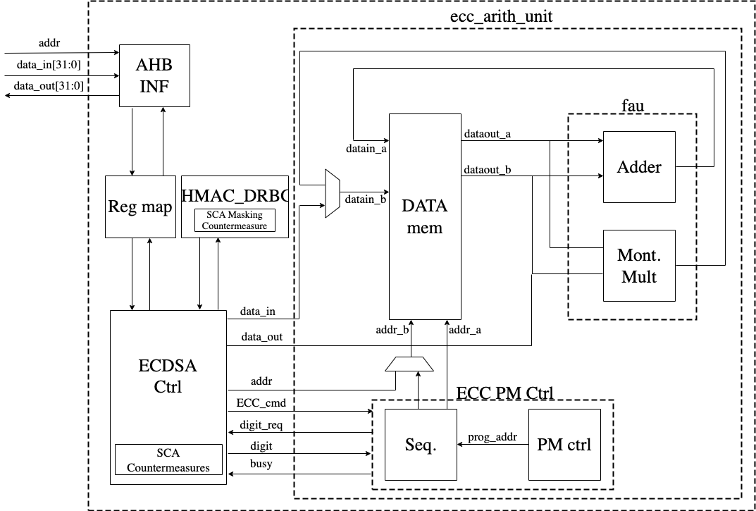
Signal descriptions
The ECDSA architecture inputs and outputs are described in the following table.
| Name | Input or output | Description |
|---|---|---|
| clk | input | All signal timings are related to the rising edge of clk. |
| reset_n | input | The reset signal is active LOW and resets the core. This is the only active LOW signal. |
| ctrl[1:0] | input | Indicates the AES type of the function. This can be: − 0b00: No Operation − 0b01: KeyGen − 0b10: Signing − 0b11: Verifying |
| zeroize | input | The core clears all internal registers to avoid any SCA information leakage. |
| seed [383:0] | input | The deterministic seed for HMAC_DRBG in the KeyGen operation. |
| nonce [383:0] | input | The deterministic nonce for HMAC_DRBG in the KeyGen operation. |
| privKey_in[383:0] | input | The input private key used in the signing operation. |
| pubKey_in[1:0][383:0] | input | The input public key(x,y) used in the verifying operation. |
| hashed_msg[383:0] | input | The hash of message using SHA384. |
| ready | output | When HIGH, the signal indicates the core is ready. |
| privKey_out[383:0] | output | The generated private key in the KeyGen operation. |
| pubKey_out[1:0][383:0] | output | The generated public key(x,y) in the KeyGen operation. |
| r[383:0] | output | The signature value of the given priveKey/message. |
| s[383:0] | output | The signature value of the given priveKey/message. |
| r’[383:0] | Output | The signature verification result. |
| valid | output | When HIGH, the signal indicates the result is ready. |
Address map
The ECDSA address map is shown here: ecc_reg — clp Reference (chipsalliance.github.io).
Pseudocode
The following pseudocode blocks demonstrate example implementations for KeyGen, Signing, and Verifying.
KeyGen
Figure 34: KeyGen pseudocode
Signing
Figure 35: Signing pseudocode
Verifying
Figure 36: Verifying pseudocode
SCA countermeasure
The described ECDSA has three main routines: KeyGen, Signing, and Verifying. Since the Verifying routine requires operation with public values rather than a secret value, our side-channel analysis does not cover this routine. Our evaluation covers the KeyGen and Signing routines where the secret values are processed.
KeyGen consists of HMAC DRBG and scalar multiplication, while Signing first requires a message hashing and then follows the same operations as KeyGen (HMAC DRBG and scalar multiplication). The last step of Signing is generating “S” as the proof of signature. Since HMAC DRBG and hash operations are evaluated separately in our document, this evaluation covers scalar multiplication and modular arithmetic operations.
Scalar multiplication
To perform the scalar multiplication, the Montgomery ladder is implemented, which is inherently resistant to timing and single power analysis (SPA) attacks.
Implementation of complete unified addition formula for the scalar multiplication avoids information leakage and enhances architecture from security and mathematical perspectives.
To protect the architecture against horizontal power/electromagnetic (EM) and differential power analysis (DPA) attacks, several countermeasures are embedded in the design [9]. Since these countermeasures require random inputs, HMAC-DRBG is fed by IV to generate these random values.
Since HMAC-DRBG generates random value in a deterministic way, firmware MUST feed different IV to ECC engine for EACH keygen and signing operation.
Base point randomization
This countermeasure is achieved using the randomized base point in projective coordinates. Hence, the base point G=(Gx, Gy) in affine coordinates is transformed and randomized to projective coordinates as (X, Y, Z) using a random value as follows:
This approach does not have the performance or area overhead because the architecture is variable-base-point implemented.
Scalar blinding
This countermeasure is achieved by randomizing the scalar as follows:
Based on [10], half of the bit size of is required to prevent advanced DPA attacks. Therefore, has 192 bits, and the blinded scalar has 576 bits. Hence, this countermeasure extends the Montgomery ladder iterations due to extended scalar.
This approach is achieved at the cost of 50% more latency on scalar multiplication and adding one lightweight block, including one 32*32 multiplier and an accumulator.
Note: the length of rand is configurable to have a trade-off between the required protection and performance.
Making countermeasures embedded into HMAC_DRBG
In the first step of the KeyGen operation, the privkey is generated using HMAC_DRBG by feeding the following two inputs: seed and nonce. To avoid SCA information leakage during this operation, we embed masking countermeasures into the HMAC_DRBG architecture.
Each round of SHA512 execution needs 6,432 random bits, and one HMAC operation needs at least 4 rounds of SHA512 operations. Furthermore, each HMAC_DRBG round needs at least 5 rounds of HMAC operations. However, the proposed architecture uses a lightweight LFSR and provides first-order DPA attack protection with negligible latency and hardware resource overhead.
ECDSA signing nonce leakage
Generating “S” as the proof of signature at the steps of the signing operation leaks where the hashed message is signed with private key and ephemeral key as follows:
Since the given message is known or the signature part r is known, the attacker can perform a known-plaintext attack. The attacker can sign multiple messages with the same key, or the attacker can observe part of the signature that is generated with multiple messages but the same key.
The evaluation shows that the CPA attack can be performed with a small number of traces, respectively. Thus, an arithmetic masked design for these operations is implemented.
Masking signature
This countermeasure is achieved by randomizing the privkey as follows:
Although computation of “S” seems the most vulnerable point in our scheme, the operation does not have a big contribution to overall latency. Hence, masking these operations has low overhead on the cost of the design.
Random number generator for SCA countermeasure
The ECC countermeasure requires several random vectors to randomize the intermediate values, as described in the preceding section. HMAC_DRBG is used to take one random vector of 384-bit (i.e., ECC_IV register) and to generate the required random vectors for different countermeasures.
The state machine of HMAC_DRBG utilization is shown in the following figure, including three main states:
- SCA random generator: Running HMAC_DRBG with IV and an internal counter to generate the required random vectors.
- KEYGEN PRIVKEY: Running HMAC_DRBG with seed and nonce to generate the privkey in KEYGEN operation.
- SIGNING NONCE: Running HMAC_DRBG based on RFC6979 in SIGNING operation with privkey and hashed_msg.
Figure 37: HMAC_DRBG utilization
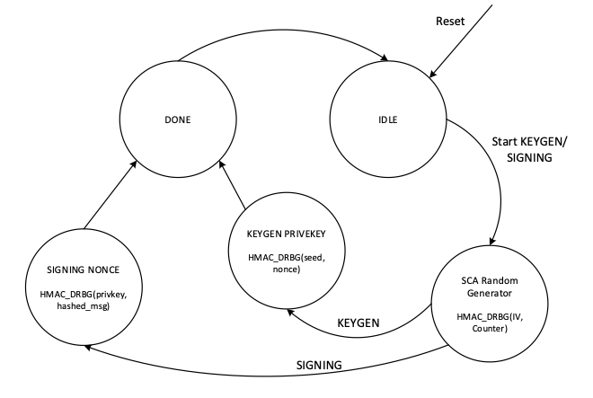
In SCA random generator state:
- This state (in KeyGen operation mode) generates 3 384-bit random vectors for the following: LFSR, base point randomization, and scalar blinding randomization.
- This state (in signing operation) generates 4 384-bit random vectors for the following: LFSR, base point randomization, scalar blinding, and masking signature randomization.
- HMAC_DRBG is initialized with IV and an internal counter. This 64-bit counter enables after reset and zeroization and contains different values depending on when ECC is called.
- HMAC_DRBG is enabled by the INIT command. To generate all required vectors, HMAC-DRBG is continued by the NEXT command that increments the built-in counter inside the HMAC-DRBG unit.
- To initialize the required seed for LFSR, LFSR_INIT_SEED is set as a constant by RTL after reset and zeroization. However, this value is updated before enabling HMAC_DRBG as follows:
- In the first execution of HMAC_DRBG after reset and zeroization, hmac_lfsr_seed is equal to LFSR_INIT_SEED XORed by internal 64-bit counter.
- In the next executions of HMAC_DRBG, hmac_lfsr_seed is equal to HMAC_DRBG output of the first execution XORed by internal 64-bit counter.
The data flow of the HMAC_DRBG operation in keygen operation mode is shown in the following figure.
Figure 38: HMAC_DRBG data flow
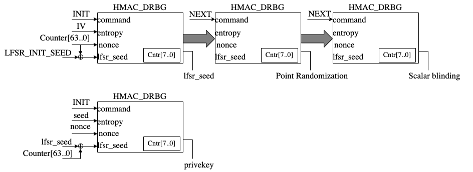
TVLA results
Test vector leakage assessment (TVLA) provides a robust test using a 𝑡-test. This test evaluates the differences between sets of acquisitions to determine if one set of measurement can be distinguished from the other. This technique can detect different types of leakages, providing a clear indication of leakage or lack thereof.
In practice, observing a t-value greater than a specific threshold (mainly 4.5) indicates the presence of leakage. However, in ECC, due to its latency, around 5 million samples are required to be captured. This latency leads to many false positives and the TVLA threshold can be considered a higher value than 4.5. Based on the following figure from “Side-Channel Analysis and Countermeasure Design for Implementation of Curve448 on Cortex-M4” by Bisheh-Niasar et. al., the threshold can be considered equal to 7 in our case.
Figure 39: TVLA threshold as a function of the number of samples per trace
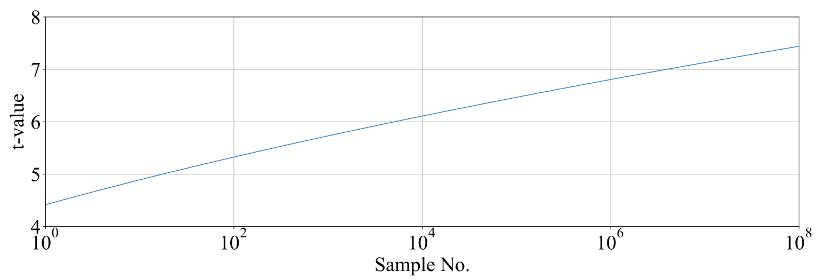
KeyGen TVLA
The TVLA results for performing seed/nonce-dependent leakage detection using 200,000 traces is shown in the following figure. Based on this figure, there is no leakage in ECC keygen by changing the seed/nonce after 200,000 operations.
Figure 40: seed/nonce-dependent leakage detection using TVLA for ECC keygen after 200,000 traces
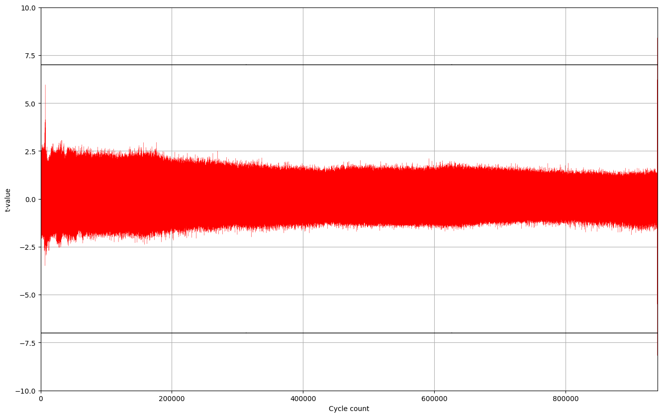
Signing TVLA
The TVLA results for performing privkey-dependent leakage detection using 20,000 traces is shown in the following figure. Based on this figure, there is no leakage in ECC signing by changing the privkey after 20,000 operations.
Figure 41: privkey-dependent leakage detection using TVLA for ECC signing after 20,000 traces
The TVLA results for performing message-dependent leakage detection using 64,000 traces is shown in the following figure. Based on this figure, there is no leakage in ECC signing by changing the message after 64,000 operations.
Figure 42: Message-dependent leakage detection using TVLA for ECC signing after 64,000 traces
The point with t-value equal to -40 is mapped to the Montgomery conversion of the message that is a publicly known value (no secret is there). By ignoring those corresponding samples, there are some sparse samples with a t-value greater than 7, as shown in the following table.
| Sample | Duration | Cycle | t-value | Operation |
|---|---|---|---|---|
| 4,746,127 | 214 | 911,381.4 | 11.2 | start of mont_conv(msg) |
| 4,746,341 | 911,422.5 | -40 | end of mont_conv(msg) | |
| 4,757,797 | 1 | 913,622.0 | 7.4 | inv_q |
| 4,768,302 | 1 | 915,639.0 | 7.8 | inv_q |
| 4,779,610 | 1 | 917,810.1 | -9.1 | inv_q |
| 4,788,120 | 1 | 919,444.0 | 7.6 | inv_q |
| 4,813,995 | 1 | 924,412.0 | 7.3 | inv_q |
| 4,822,693 | 1 | 926,082.1 | 7.5 | inv_q |
| 4,858,671 | to the end | 932,989.8 | -7.6 | Ended ECC signing |
Performance
The ECC core performance is reported in the next section.
Pure hardware architecture
In this architecture, the ECC interface and controller are implemented in hardware. The performance specification of the ECC architecture is reported as shown in the following table.
| Operation | Cycle count [CCs] | Time [ms] @ 400 MHz | Throughput [op/s] |
|---|---|---|---|
| Keygen | 909,648 | 2.274 | 439 |
| Signing | 932,990 | 2.332 | 428 |
| Verifying | 1,223,938 | 3.060 | 326 |
LMS Accelerator
LMS cryptography is a type of hash-based digital signature scheme that was standardized by NIST in 2020. It is based on the Leighton-Micali Signature (LMS) system, which uses a Merkle tree structure to combine many one-time signature (OTS) keys into a single public key. LMS cryptography is resistant to quantum attacks and can achieve a high level of security without relying on large integer mathematics.
Caliptra supports only LMS verification using a software/hardware co-design approach. Hence, the LMS accelerator reuses the SHA256 engine to speedup the Winternitz chain by removing software-hardware interface overhead. The LMS-OTS verification algorithm is shown in follwoing figure:
Figure 43: LMS-OTS Verification algorithm
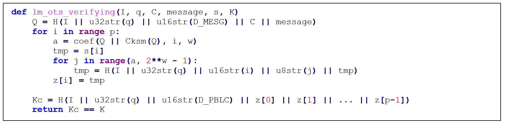
The high-level architecture of LMS is shown in the following figure.
Figure 44: LMS high-level architecture
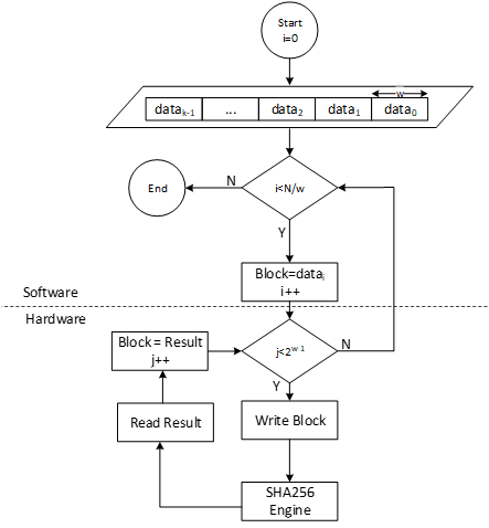
LMS parameters
LMS parameters are shown in the following table:
| Parameter | Description | Value |
|---|---|---|
| n | The number of bytes of the output of the hash function. | {24, 32} |
| w | The width (in bits) of the Winternitz coefficients. | {1, 2, 4, 8} |
| p | The number of n-byte string elements that make up the LM-OTS signature. | {265, 133, 67, 34} |
| H | A cryptographic hash function. | SHA256 |
| h | The height of the tree. | {5, 10, 15, 20, 25} |
- SHA256 is used for n=32 and SHA256/192 is used for n=24.
- SHAKE256 is not supported in this architecture.
- Value of p is determined based on w. If w=1, p is equal to 265, and so on.
Winternitz Chain Accelerator
The Winternitz hash chain can be accelerated in hardware to enhance the performance of the design. For that, a configurable architecture is proposed that can reuse SHA256 engine. The LMS accelerator architecture is shown in the following figure, while H is SHA256 engine.
Figure 45: Winternitz chain architecture
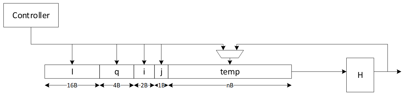
Signal descriptions
The LMS accelerator integrated into SHA256 architecture inputs and outputs are described as follows.
| Name | Input or output | Description |
|---|---|---|
| clk | input | All signal timings are related to the rising edge of clk. |
| reset_n | input | The reset signal is active LOW and resets the core. This is the only active LOW signal. |
| init | input | The core is initialized and processes the first block of message. |
| next | input | The core processes the rest of the message blocks using the result from the previous blocks. |
| mode | input | Indicates the hash type of the function. This can be: - SHA256/224 - SHA256 |
| zeroize | input | The core clears all internal registers to avoid any SCA information leakage. |
| WNTZ_MODE | input | SHA256 core is configured in Winternitz verification mode. |
| WNTZ_W[3:0] | input | Winternitz W value. |
| WNTZ_N_MODE | input | Winternitz n value(SHA192/SHA256 --> n = 24/32) |
| block[511:0] | input | The input padded block of message. |
| ready | output | When HIGH, the signal indicates the core is ready. |
| digest[255:0] | output | The hashed value of the given block. |
| digest_valid | output | When HIGH, the signal indicates the result is ready. |
Address map
The address map for LMS accelerator integrated into SHA256 is shown here: sha256_reg — clp Reference (chipsalliance.github.io).
PCR vault
- Platform Configuration Register (PCR) vault is a register file that stores measurements to be used by the microcontroller.
- PCR entries are read-only registers of 384 bits each.
- Control bits allow for entries to be cleared by FW, which sets their values back to 0.
- A lock bit can be set by FW to prevent the entry from being cleared. The lock bit is sticky and only resets on a powergood cycle.
| PCRV register | Address Offset | Description |
|---|---|---|
| PCR Control[31:0] | 0x1001a000 | 32 Control registers, 32 bits each |
| PCR Entry[31:0][11:0][31:0] | 0x1001a600 | 32 PCR entries, 384 bits each |
PCR vault functional block
PCR entries are hash extended using a hash extension function. The hash extension function takes the data currently in the PCR entry specified, concatenates data provided by the FW, and performs a SHA384 function on that data, storing the result back into the same PCR entry.
PCR hash extend function
FW provides the PCR entry to use as source and destination of the hash extend. HW copies the PCR into the start of the SHA block and locks those dwords from FW access. FW then provides the new data, and runs the SHA function as usual. After initialization, the locked dwords are unlocked.
FW must set a last cycle flag before running the last iteration of the SHA engine. This could be the first “init” cycle, or the Nth “next” cycle. This flag allows HW to copy the final resulting hash output back to the source PCR.
PCR signing
- PCR signing uses the key in key slot index 7 for PCR signing
- HW implements a HW function called GEN_PCR_HASH
- HW reads all the PCRs from all the PCR slots and hash extends them along with the NONCE that Caliptra FW provides
- PCR Hash = Hash(PCR[0], …, PCR[31], Nonce)
- HW also implements a HW function called SIGN_PCR. This function takes the PCR digest that was generated by the previous routine and signs it using the key in key slot 7, following the same ECC sign flow defined in the ECC section.
- The resulting PCR DIGEST is used only once for signing by the HW. If a new PCR signing is required, GEN_PCR_HASH needs to be redone.
Key vault
Key Vault (KV) is a register file that stores the keys to be used by the microcontroller, but this register file is not observed by the microcontroller. Each cryptographic function has a control register and functional block designed to read from and write to the KV.
| KV register | Description |
|---|---|
| Key Control[31:0] | 32 Control registers, 32 bits each |
| Key Entry[31:0][11:0][31:0] | 32 Key entries, 384 bits each No read or write access |
Key vault functional block
Keys and measurements are stored in 512b register files. These have no read or write path from the microcontroller. The entries are read through a passive read mux driven by each cryptographic block. Locked entries return zeroes.
Entries in the KV must be cleared via control register, or by de-assertion of pwrgood.
Each entry has a control register that is writable by the microcontroller.
The destination valid field is programmed by FW in the cryptographic block generating the key, and it is passed here at generation time. This field cannot be modified after the key is generated and stored in the KV.
| KV Entry Ctrl Fields | Reset | Description |
|---|---|---|
| Lock wr[0] | core_only_rst_b | Setting the lock wr field prevents the entry from being written by the microcontroller. Keys are always locked. After a lock is set, it cannot be reset until cptra_rst_b is de-asserted. |
| Lock use[1] | core_only_rst_b | Setting the lock use field prevents the entry from being used in any cryptographic blocks. After the lock is set, it cannot be reset until cptra_rst_b is de-asserted. |
| Clear[2] | cptra_rst_b | If unlocked, setting the clear bit causes KV to clear the associated entry. The clear bit is reset after entry is cleared. |
| Copy[3] | cptra_rst_b | ENHANCEMENT: Setting the copy bit causes KV to copy the key to the entry written to Copy Dest field. |
| Copy Dest[8:4] | cptra_rst_b | ENHANCEMENT: Destination entry for the copy function. |
| Dest_valid[16:9] | hard_reset_b | KV entry can be used with the associated cryptographic block if the appropriate index is set. [0] - HMAC KEY [1] - HMAC BLOCK [2] - SHA BLOCK [2] - ECC PRIVKEY [3] - ECC SEED [7:5] - RSVD |
| last_dword[20:19] | hard_reset_b | Store the offset of the last valid dword, used to indicate the last cycle for read operations. |
Key vault cryptographic functional block
A generic block is instantiated in each cryptographic block to enable access to KV.
Each input to a cryptographic engine can have a key vault read block associated with it. The KV read block takes in a key vault read control register that drives an FSM to copy an entry from the key vault into the appropriate input register of the cryptographic engine.
Each output generated by a cryptographic engine can have its result copied to a slot in the key vault. The KV write block takes in a key vault write control register. This register drives an FSM to copy the result from the cryptographic engine into the appropriate key vault entry. It also programs a control field for that entry to indicate where that entry can be used.
After programming the key vault read control, FW needs to query the associated key vault read status to confirm that the requested key was copied successfully. After valid is set and the error field reports success, the key is ready to be used.
Similarly, after programming the key vault write control and initiating the cryptographic function that generates the key to be written, FW needs to query the associated key vault write status to confirm that the requested key was generated and written successfully.
When a key is read from the key vault, the API register is locked and any result generated from the cryptographic block is not readable by firmware. The digest can only be sent to the key vault by appropriately programming the key vault write controls. After the cryptographic block completes its operation, the lock is cleared and the key is cleared from the API registers.
If multiple iterations of the cryptographic function are required, the key vault read and write controls must be programmed for each iteration. This ensures that the lock is set and the digest is not readable.
The following tables describe read, write, and status values for key vault blocks.
| KV Read Ctrl Reg | Description |
|---|---|
| read_en[0] | Indicates that the read data is to come from the key vault. Setting this bit to 1 initiates copying of data from the key vault. |
| read_entry[5:1] | Key vault entry to retrieve the read data from the engine. |
| pcr_hash_extend[6] | Requested entry is a PCR. This is used only for the SHA engine to hash extend. It is not functional in any other cryptographic engine. |
| rsvd[31:7] | Reserved field |
| KV Write Ctrl Reg | Description |
|---|---|
| write_en[0] | Indicates that the result is to be stored in the key vault. Setting this bit to 1 copies the result to the key vault when it is ready. |
| write_entry[5:1] | Key vault entry to store the result. |
| hmac_key_dest_valid[6] | HMAC KEY is a valid destination. |
| hmac_block_dest_valid[7] | HMAC BLOCK is a valid destination. |
| sha_block_dest_valid[8] | SHA BLOCK is a valid destination. |
| ecc_pkey_dest_valid[9] | ECC PKEY is a valid destination. |
| ecc_seed_dest_valid[10] | ECC SEED is a valid destination. |
| rsvd[31:11] | Reserved field |
| KV Status Reg | Description |
|---|---|
| ready[0] | Key vault control is idle and ready for a command. |
| valid[1] | Requested flow is done. |
| error[9:2] | SUCCESS - 0x0 - Key Vault flow was successful KV_READ_FAIL - 0x1 - Key Vault Read flow failed KV_WRITE_FAIL - 0x2 - Key Vault Write flow failed |
De-obfuscation engine
To protect software intellectual property from different attacks and, particularly, for thwarting an array of supply chain threats, code obfuscation is employed. Hence, the de-obfuscation engine is implemented to decrypt the code.
Advanced Encryption Standard (AES) is used as a de-obfuscation function to encrypt and decrypt data [4]. The hardware implementation is based on Secworks/aes [1]. The implementation supports the two variants: 128- and 256-bit keys with a block/chunk size of 128 bits.
The AES algorithm is described as follows:
- The key is fed to an AES core to compute and initialize the round key
- The message is broken into 128-bit chunks by the host
- For each chunk:
- The message is fed to the AES core
- The AES core and its working mode (enc/dec) are triggered by the host
- The AES core status is changed to ready after encryption or decryption processing
- The result digest can be read before processing the next message chunks
Key vault de-obfuscation block operation
A de-obfuscation engine (DOE) is used in conjunction with AES cryptography to de-obfuscate the UDS and field entropy.
- The obfuscation key is driven to the AES key. The data to be decrypted (either obfuscated UDS or obfuscated field entropy) is fed into the AES data.
- An FSM manually drives the AES engine and writes the decrypted data back to the key vault.
- FW programs the DOE with the requested function (UDS or field entropy de-obfuscation), and the destination for the result.
- After de-obfuscation is complete, FW can clear out the UDS and field entropy values from any flops until cptra_pwrgood de-assertion.
The following tables describe DOE register and control fields.
| DOE Register | Address | Description |
|---|---|---|
| IV | 0x10000000 | 128 bit IV for DOE flow. Stored in big-endian representation. |
| CTRL | 0x10000010 | Controls for DOE flows. |
| STATUS | 0x10000014 | Valid indicates the command is done and results are stored in key vault. Ready indicates the core is ready for another command. |
| DOE Ctrl Fields | Reset | Description |
|---|---|---|
| COMMAND[1:0] | Cptra_rst_b | 2’b00 Idle 2’b01 Run UDS flow 2’b10 Run FE flow 2’b11 Clear Obf Secrets |
| DEST[4:2] | Cptra_rst_b | Destination register for the result of the de-obfuscation flow. Field entropy writes into DEST and DEST+1 Key entry only, can’t go to PCR . |
Key vault de-obfuscation flow
- ROM loads IV into DOE. ROM writes to the DOE control register the destination for the de-obfuscated result and sets the appropriate bit to run UDS and/or the field entropy flow.
- DOE state machine takes over and loads the Caliptra obfuscation key into the key register.
- Next, either the obfuscated UDS or field entropy are loaded into the block register 4 DWORDS at a time.
- Results are written to the KV entry specified in the DEST field of the DOE control register.
- State machine resets the appropriate RUN bit when the de-obfuscated key is written to KV. FW can poll this register to know when the flow is complete.
- The clear obf secrets command flushes the obfuscation key, the obfuscated UDS, and the field entropy from the internal flops. This should be done by ROM after both de-obfuscation flows are complete.
Data vault
Data vault is a set of generic scratch pad registers with specific lock functionality and clearable on cold and warm resets.
- 48B scratchpad registers that are lockable but cleared on cold reset (10 registers)
- 48B scratchpad registers that are lockable but cleared on warm reset (10 registers)
- 4B scratchpad registers that are lockable but cleared on cold reset (8 registers)
- 4B scratchpad registers that are lockable but cleared on warm reset (10 registers)
- 4B scratchpad registers that are cleared on warm reset (8 registers)
Cryptographic blocks fatal and non-fatal errors
The following table describes cryptographic errors.
| Errors | Error type | Description |
|---|---|---|
| ECC_R_ZERO | HW_ERROR_NON_FATAL | Indicates a non-fatal error in ECC signing if the computed signature R is equal to 0. FW should change the message or privkey to perform a valid signing. |
| CRYPTO_ERROR | HW_ERROR_FATAL | Indicates a fatal error due to multiple cryptographic operations occurring simultaneously. FW must only operate one cryptographic engine at a time. |
Terminology
The following terminology is used in this document.
| Abbreviation | Description |
|---|---|
| AES | Advanced Encryption Standard |
| BMC | Baseboard Management Controller |
| CA | Certificate Authority |
| CDI | Composite Device Identifier |
| CPU | Central Processing Unit |
| CRL | Certificate Revocation List |
| CSR | Certificate Signing Request |
| CSP | Critical Security Parameter |
| DICE | Device Identifier Composition Engine |
| DME | Device Manufacturer Endorsement |
| DPA | Differential Power Analysis |
| DRBG | Deterministic Random Bit Generator |
| DWORD | 32-bit (4-byte) data element |
| ECDSA | Elliptic Curve Digital Signature Algorithm |
| FMC | FW First Mutable Code |
| FSM | Finite State Machine |
| GPU | Graphics Processing Unit |
| HMAC | Hash-based message authentication code |
| IDevId | Initial Device Identifier |
| iRoT | Internal RoT |
| IV | Initial Vector |
| KAT | Known Answer Test |
| KDF | Key Derivation Function |
| LDevId | Locally Significant Device Identifier |
| MCTP | Management Component Transport Protocol |
| NIC | Network Interface Card |
| NIST | National Institute of Standards and technology |
| OCP | Open Compute Project |
| OTP | One-time programmable |
| PCR | Platform Configuration Register |
| PKI | Public Key infrastructure |
| PUF | Physically unclonable function |
| RNG | Random Number Generator |
| RoT | Root of Trust |
| RTI | RoT for Identity |
| RTM | RoT for Measurement |
| RTR | RoT for Reporting |
| SCA | Side-Channel Analysis |
| SHA | Secure Hash Algorithm |
| SoC | System on Chip |
| SPA | Simple Power Analysis |
| SPDM | Security Protocol and Data Model |
| SSD | Solid State Drive |
| TCB | Trusted Computing Base |
| TCI | TCB Component Identifier |
| TCG | Trusted Computing Group |
| TEE | Trusted Execution Environment |
| TRNG | True Random Number Generator |
| UECC | Uncorrectable Error Correction Code |
References
- J. Strömbergson, "Secworks," [Online]. Available at https://github.com/secworks.
- NIST, Federal Information Processing Standards Publication (FIPS PUB) 180-4 Secure Hash Standard (SHS).
- OpenSSL [Online]. Available at https://www.openssl.org/docs/man3.0/man3/SHA512.html.
- N. W. Group, RFC 3394, Advanced Encryption Standard (AES) Key Wrap Algorithm, 2002.
- NIST, Federal Information Processing Standards Publication (FIPS) 198-1, The Keyed-Hash Message Authentication Code, 2008.
- N. W. Group, RFC 4868, Using HMAC-SHA256, HMAC-SHA384, and HMAC-SHA512 with IPsec, 2007.
- RFC 6979, Deterministic Usage of the Digital Signature Algorithm (DSA) and Elliptic Curve Digital Signature Algorithm (ECDSA), 2013.
- TCG, Hardware Requirements for a Device Identifier Composition Engine, 2018.
- Coron, J.-S.: Resistance against differential power analysis for elliptic curve cryptosystems. In: Ko¸c, C¸ .K., Paar, C. (eds.) CHES 1999. LNCS, vol. 1717, pp. 292–302.
- Schindler, W., Wiemers, A.: Efficient side-channel attacks on scalar blinding on elliptic curves with special structure. In: NISTWorkshop on ECC Standards (2015).
- National Institute of Standards and Technology, "Digital Signature Standard (DSS)", Federal Information Processing Standards Publication (FIPS PUB) 186-4, July 2013.
- NIST SP 800-90A, Rev 1: "Recommendation for Random Number Generation Using Deterministic Random Bit Generators", 2012. |
- CHIPS Alliance, “RISC-V VeeR EL2 Programmer’s Reference Manual” [Online] Available at https://github.com/chipsalliance/Cores-VeeR-EL2/blob/main/docs/RISC-V_VeeR_EL2_PRM.pdf.
- “The RISC-V Instruction Set Manual, Volume I: User-Level ISA, Document Version 20191213”, Editors Andrew Waterman and Krste Asanovi ́c, RISC-V Foundation, December 2019. Available at https://riscv.org/technical/specifications/.
- “The RISC-V Instruction Set Manual, Volume II: Privileged Architecture, Document Version 20211203”, Editors Andrew Waterman, Krste Asanovi ́c, and John Hauser, RISC-V International, December 2021. Available at https://riscv.org/technical/specifications/.
[1] Caliptra.** **Spanish for “root cap” and describes the deepest part of the root
5f85fb4
![]()
Caliptra Integration Specification
Version 1.1
Scope
This document describes the Caliptra hardware implementation requirements, details, and release notes. This document is intended for a high-level overview of the IP used in Caliptra.
This document is not intended for any micro-architectural design specifications. Detailed information on each of the IP components are shared in individual documents, where applicable.
Overview
This document contains high level information on the Caliptra hardware design. The details include open-source IP information, configuration settings for open-source IP (if applicable), and IP written specifically for Caliptra.
For more information, see Caliptra: A Datacenter System on a Chip (SoC) Root of Trust (RoT).
References and related specifications
The blocks described in this document are either obtained from open-source GitHub repositories, developed from scratch, or modification of open-source implementations. Links to relevant documentation and GitHub sources are shared in the following table.
Table 1: Related specifications
| IP/Block | GitHub URL | Documentation | Link |
|---|---|---|---|
| Cores-VeeR | GitHub - chipsalliance/Cores-VeeR-EL2 | VeeR EL2 Programmer’s Reference Manual | chipsalliance/Cores-VeeR-EL2 · GitHubPDF |
| AHB Lite Bus | aignacio/ahb_lite_bus: AHB Bus lite v3.0 (github.com) | AHB Lite Protocol Figure 1: SoC interface block diagram | ahb_lite_bus/docs at master · aignacio/ahb_lite_bus (github.com) ahb_lite_bus/diagram_ahb_bus.png at master · aignacio/ahb_lite_bus (github.com) |
| SHA 256 | secworks/sha256: Hardware implementation of the SHA-256 cryptographic hash function (github.com) | ||
| SHA 512 | |||
| SPI Controller | https://github.com/pulp-platform/axi_spi_master |
Caliptra Core
For information on the Caliptra Core, see the High level architecture section of Caliptra: A Datacenter System on a Chip (SoC) Root of Trust (RoT).
SoC interface definition
The following figure shows the SoC interface definition.
Figure 1: SoC Interface Block Diagram
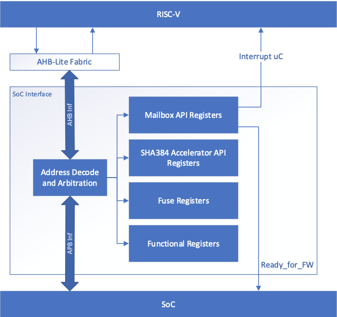
Integration parameters
The following table describes integration parameters.
Table 2: Integration parameters
| Parameter name | Width | Defines file | Description |
|---|---|---|---|
| CPTRA_SET_MBOX_PAUSER_INTEG | 5 | soc_ifc_pkg.sv | Each bit hardcodes the valid PAUSER for mailbox at integration time. |
| CPTRA_MBOX_VALID_PAUSER | [4:0][31:0] | soc_ifc_pkg.sv | Each parameter corresponds to a hardcoded valid PAUSER value for mailbox, set at integration time. Must set corresponding bit in the CPTRA_SET_MBOX_PAUSER_INTEG parameter for this valid pauser override to be used. |
| CPTRA_DEF_MBOX_VALID_PAUSER | 32 | soc_ifc_pkg.sv | Sets the default valid PAUSER for mailbox accesses. This PAUSER is valid at all times. |
| CPTRA_SET_FUSE_PAUSER_INTEG | 1 | soc_ifc_pkg.sv | Sets the valid PAUSER for fuse accesses at integration time. |
| CPTRA_FUSE_VALID_PAUSER | 32 | soc_ifc_pkg.sv | Overrides the programmable valid PAUSER for fuse accesses when CPTRA_SET_FUSE_PAUSER_INTEG is set to 1. |
Table 3: Integration Defines
| Defines | Defines file | Description |
|---|---|---|
| CALIPTRA_INTERNAL_TRNG | config_defines.svh | Defining this enables the internal TRNG source. |
| CALIPTRA_INTERNAL_UART | config_defines.svh | Defining this enables the internal UART. |
| CALIPTRA_INTERNAL_QSPI | config_defines.svh | Defining this enables the internal QSPI. |
| USER_ICG | config_defines.svh | If added by an integrator, provides the name of the custom clock gating module that is used in clk_gate.sv. USER_ICG replaces the clock gating module, CALIPTRA_ICG, defined in caliptra_icg.sv. This substitution is only performed if integrators also define TECH_SPECIFIC_ICG. |
| TECH_SPECIFIC_ICG | config_defines.svh | Defining this causes the custom, integrator-defined clock gate module (indicated by the USER_ICG macro) to be used in place of the native Caliptra clock gate module. |
| USER_EC_RV_ICG | config_defines.svh | If added by an integrator, provides the name of the custom clock gating module that is used in the RISC-V core. USER_EC_RV_ICG replaces the clock gating module, TEC_RV_ICG, defined in beh_lib.sv. This substitution is only performed if integrators also define TECH_SPECIFIC_EC_RV_ICG. |
| TECH_SPECIFIC_EC_RV_ICG | config_defines.svh | Defining this causes the custom, integrator-defined clock gate module (indicated by the USER_EC_RV_ICG macro) to be used in place of the native RISC-V core clock gate module. |
Interface
The following tables describe the interface signals.
Table 4: Clocks and resets
| Signal name | Width | Driver | Synchronous (as viewed from Caliptra’s boundary) | Description |
|---|---|---|---|---|
| cptra_pwrgood | 1 | Input | Asynchronous Assertion Synchronous deassertion to clk | Active high power good indicator. Deassertion hard resets Caliptra. |
| cptra_rst_b | 1 | Input | Asynchronous Assertion Synchronous deassertion to clk | Active low asynchronous reset. |
| clk | 1 | Input | Convergence and validation done at 400MHz. All other frequencies are up to the user. |
Table 5: APB Interface
| Signal name | Width | Driver | Synchronous (as viewed from Caliptra’s boundary) | Description |
|---|---|---|---|---|
| PADDR | CALIPTRA_APB_ADDR_WIDTH | Input | Synchronous to clk | Address bus |
| PPROT | 3 | Input | Synchronous to clk | Protection level |
| PSEL | 1 | Input | Synchronous to clk | Select line |
| PENABLE | 1 | Input | Synchronous to clk | Indicates the second and subsequent cycles. |
| PWRITE | 1 | Input | Synchronous to clk | Indicates transfer is a write when high or a read when low. |
| PWDATA | CALIPTRA_APB_DATA_WIDTH | Input | Synchronous to clk | Write data bus |
| PAUSER | CALIPTRA_APB_USER_WIDTH | Input | Synchronous to clk | Sideband signal indicating requestor ID for transfer. |
| PREADY | 1 | Output | Synchronous to clk | Used to extend an APB transfer by completer. |
| PRDATA | CALIPTRA_APB_DATA_WIDTH | Output | Synchronous to clk | Read data bus |
| PSLVERR | 1 | Output | Synchronous to clk | Transfer error |
Table 6: QSPI signals
| Signal name | Width | Driver | Synchronous (as viewed from Caliptra’s boundary) | Description |
|---|---|---|---|---|
| qspi_clk_o | 1 | Output | QSPI clock | |
| qspi_cs_no | 2 | Output | Synchronous to qspi_clk_o | QSPI chip select |
| qspi_d_i | 4 | Input | Synchronous to qspi_clk_o | QSPI data lanes for receiving data. |
| qspi_d_o | 4 | Output | Synchronous to qspi_clk_o | QSPI data output lanes for sending opcode and address. |
| qspi_d_en_o | 4 | Output | Synchronous to qspi_clk_o | QSPI enable pins to control data direction. |
Table 7: Mailbox notifications
| Signal name | Width | Driver | Synchronous (as viewed from Caliptra’s boundary) | Description |
|---|---|---|---|---|
| ready_for_fuses | 1 | Output | Synchronous to clk | Indicates that Caliptra is ready for fuse programming. |
| ready_for_fw_push | 1 | Output | Synchronous to clk | Indicates that Caliptra is ready for firmware. |
| ready_for_runtime | 1 | Output | Synchronous to clk | Indicates that Caliptra firmware is ready for RT flow. |
| mailbox_data_avail | 1 | Output | Synchronous to clk | Indicates that the mailbox has data for SoC to read (reflects the value of the register). |
| mailbox_flow_done | 1 | Output | Synchronous to clk | Indicates that the mailbox flow is complete (reflects the value of the register). |
Table 8: SRAM interface
| Signal name | Width | Driver | Synchronous (as viewed from Caliptra’s boundary) | Description |
|---|---|---|---|---|
| mbox_sram_cs | 1 | Output | Synchronous to clk | Chip select for mbox SRAM |
| mbox_sram_we | 1 | Output | Synchronous to clk | Write enable for mbox SRAM |
| mbox_sram_addr | MBOX_ADDR_W | Output | Synchronous to clk | Addr lines for mbox SRAM |
| mbox_sram_wdata | MBOX_DATA_W | Output | Synchronous to clk | Write data for mbox SRAM |
| mbox_sram_rdata | MBOX_DATA_W | Input | Synchronous to clk | Read data for mbox SRAM |
| imem_cs | 1 | Output | Synchronous to clk | Chip select for imem SROM |
| imem_addr | IMEM_ADDR_WIDTH | Output | Synchronous to clk | Addr lines for imem SROM |
| imem_rdata | IMEM_DATA_WIDTH | Input | Synchronous to clk | Read data for imem SROM |
| iccm_clken | ICCM_NUM_BANKS | Input | Synchronous to clk | Per-bank clock enable |
| iccm_wren_bank | ICCM_NUM_BANKS | Input | Synchronous to clk | Per-bank write enable |
| iccm_addr_bank | ICCM_NUM_BANKS x (ICCM_BITS-4) | Input | Synchronous to clk | Per-bank address |
| iccm_bank_wr_data | ICCM_NUM_BANKS x 39 | Input | Synchronous to clk | Per-bank input data |
| iccm_bank_dout | ICCM_NUM_BANKS x 39 | Output | Synchronous to clk | Per-bank output data |
| dccm_clken | DCCM_NUM_BANKS | Input | Synchronous to clk | Per-bank clock enable |
| dccm_wren_bank | DCCM_NUM_BANKS | Input | Synchronous to clk | Per-bank write enable |
| dccm_addr_bank | DCCM_NUM_BANKS x (DCCM_BITS-4) | Input | Synchronous to clk | Per-bank address |
| dccm_wr_data_bank | DCCM_NUM_BANKS x DCCM_FDATA_WIDTH | Input | Synchronous to clk | Per-bank input data |
| dccm_bank_dout | DCCM_NUM_BANKS x DCCM_FDATA_WIDTH | Output | Synchronous to clk | Per-bank output data |
Table 9: JTAG interface
| Signal name | Width | Driver | Synchronous (as viewed from Caliptra’s boundary) | Description |
|---|---|---|---|---|
| jtag_tck | 1 | input | ||
| jtag_tms | 1 | input | Synchronous to jtag_tck | |
| jtag_tdi | 1 | input | Synchronous to jtag_tck | |
| jtag_trst_n | 1 | input | Asynchronous assertion Synchronous deassertion to jtag_tck | |
| jtag_tdo | 1 | output | Synchronous to jtag_tck |
Table 10: UART interface
| Signal name | Width | Driver | Synchronous (as viewed from Caliptra’s boundary) | Description |
|---|---|---|---|---|
| uart_tx | 1 | output | UART transmit pin | |
| uart_rx | 1 | input | UART receive pin |
Table 11: Security and miscellaneous
| Signal name | Width | Driver | Synchronous (as viewed from Caliptra’s boundary) | Description |
|---|---|---|---|---|
| CPTRA_OBF_KEY | 256 | Input Strap | Asynchronous | Obfuscation key is driven by SoC at integration time. Ideally this occurs just before tape-in and the knowledge of this key must be protected unless PUF is driving this. The key is latched by Caliptra on caliptra powergood deassertion. It is cleared after its use and can only re-latched on a power cycle (powergood deassertion to assertion). |
| SECURITY_STATE | 3 | Input Strap | Synchronous to clk | Security state that Caliptra should take (for example, manufacturing, secure, unsecure, etc.). The key is latched by Caliptra on cptra_noncore_rst_b deassertion. Any time the state changes to debug mode, all keys, assets, and secrets stored in fuses or key vault are cleared. Cryptography core states are also flushed if they were being used. |
| scan_mode | 1 | Input Strap | Synchronous to clk | Must be set before entering scan mode. This is a separate signal than the scan chain enable signal that goes into scan cells. This allows Caliptra to flush any assets or secrets present in key vault and flops if the transition is happening from a secure state. |
| GENERIC_INPUT_WIRES | 64 | Input | Synchronous to clk | Placeholder of input wires for late binding features. These values are reflected into registers that are exposed to firmware. |
| GENERIC_OUTPUT_WIRES | 64 | Output | Synchronous to clk | Placeholder of output wires for late binding features. Firmware can set the wires appropriately via register writes. |
| CALIPTRA_ERROR_FATAL | 1 | Output | Synchronous to clk | Indicates a fatal error from Caliptra. |
| CALIPTRA_ERROR_NON_FATAL | 1 | Output | Synchronous to clk | Indicates a non fatal error from Caliptra. |
| BootFSM_BrkPoint | 1 | Input Strap | Asynchronous | Stops the BootFSM to allow TAP writes set up behavior. Examples of these behaviors are skipping or running ROM flows, or stepping through BootFSM. |
| eTRNG_REQ | 1 | Output | Synchronous to clk | External source mode: TRNG_REQ to SoC. SoC writes to TRNG architectural registers with a NIST-compliant entropy. Internal source mode: TRNG_REQ to SoC. SoC enables external RNG digital bitstream input into iTRNG_DATA/iTRNG_VALID. |
| iTRNG_DATA | 4 | Input | Synchronous to clk | External source mode: Not used. Internal source mode only: Physical True Random Noise Source (PTRNG for "Number Generator") digital bit stream from SoC, which is sampled when iTRNG_VALID is high. See the Hardware Specification for details on PTRNG expectations and iTRNG entropy capabilities. |
| iTRNG_VALID | 1 | Input | Synchronous to clk | External source mode: Not used. Internal source mode only: RNG bit valid. This is valid per transaction. iTRNG_DATA can be sampled whenever this bit is high. The expected iTRNG_VALID output rate is about 50KHz. |
Architectural registers and fuses
Control registers and fuses are documented on GitHub.
- External Registers: caliptra_top_reg — caliptra_top_reg Reference (chipsalliance.github.io)
- Internal Registers - clp — clp Reference (chipsalliance.github.io)
Fuses
Fuses are writable only one time and require a cptra_pwrgood to be recycled to be written again.
After all fuses are written, the fuse done register at the end of the fuse address space must be set to 1 to lock the fuse writes and to proceed with the boot flow.
Although fuse values (and the fuse done register) persist across a warm reset, SoC is still required to perform a write to the fuse done register while in the BOOT_FUSE state in order to complete the bringup from reset. See 6.1 Boot FSM for further details.
Interface rules
The following figure shows the reset rules and timing for cold boot flows.
Figure 2: Reset rules and timing diagram
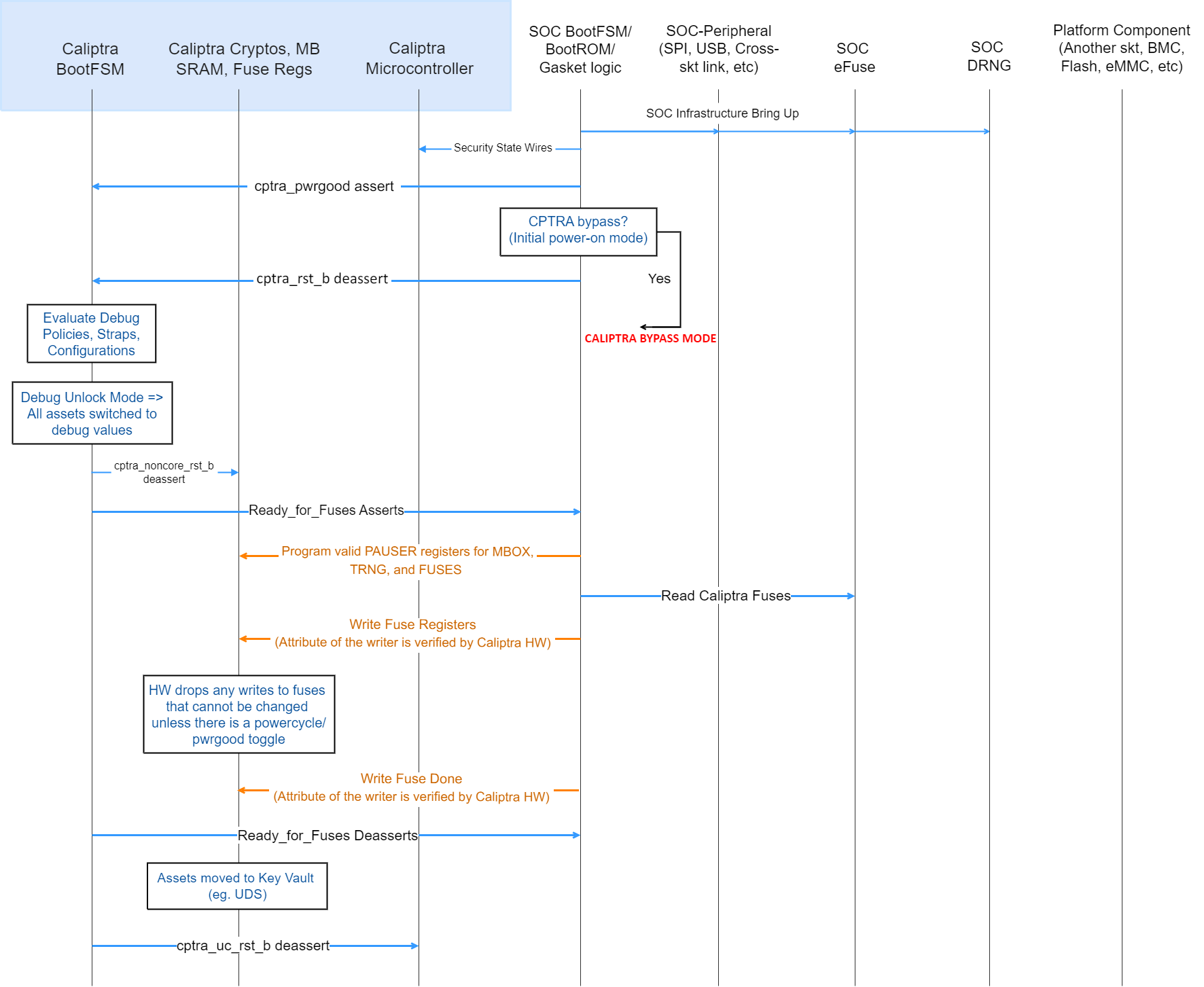
Deassertion of cptra_pwrgood indicates a power cycle that results in returning Caliptra to its default state. All resettable flops are reset.
Deassertion of cptra_rst_b indicates a warm reset cycle that resets all but the “sticky” registers (fuses, error logging, etc.).
Assertion of BootFSM_BrkPoint stops the boot flow from releasing Caliptra from reset after fuse download. Writing a 1 to the GO field of the CPTRA_BOOTFSM_GO register allows the boot flow to proceed.
APB arbitration
Caliptra is a client on the APB bus, incapable of initiating transfers. If SoCs have multiple APBs or other proprietary-fabric protocols that require any special fabric arbitration, that arbitration is done at SoC level.
Undefined address accesses
All accesses that are outside of the defined address space of Caliptra are responded to by Caliptra’s SoC interface:
- All reads to undefined addresses get completions with zero data.
- All writes to undefined addresses are dropped.
- All other undefined opcodes are silently dropped.
- Access to mailbox memory region with invalid PAUSER are dropped.
- Access to a fuse with invalid PAUSER are dropped.
- PSLVERR is asserted for any of the above conditions.
All accesses must be 32-bit aligned. Misaligned writes are dropped and reads return 0x0.
Undefined mailbox usages
A trusted/valid requester that locks the mailbox and never releases the lock will cause the mailbox to be locked indefinitely.
Caliptra firmware internally has the capability to force release the mailbox based on various timers but there is no architectural requirement to use this capability.
Straps
Straps are signal inputs to Caliptra that are sampled once on reset exit, and the latched value persists throughout the remaining uptime of the system. Straps are sampled on either caliptra pwrgood signal deassertion or cptra_noncore_rst_b deassertion – refer to interface table for list of straps.
Obfuscation key
SoC drives the key at the tape-in time of the SoC using an Engineering Change Order (ECO) and must be protected from common knowledge. For a given SoC construction, this can be driven using a PUF too.
The key must follow the security rules defined in the Caliptra architectural specification.
SoC must ensure that there are no SCAN cells on the flops that latch this key internally to Caliptra.
Late binding interface signals
The interface signals GENERIC_INPUT_WIRES and GENERIC_OUTPUT_WIRES are placeholders on the SoC interface reserved for late binding features. This may include any feature that is required for correct operation of the design in the final integrated SoC and that may not be accommodated through existing interface signaling (such as the mailbox).
While these late binding interface pins are generic in nature until assigned a function, integrators must not define non-standard use cases for these pins. Defining standard use cases ensures that the security posture of Caliptra in the final implementation is not degraded relative to the consortium design intent. Bits in GENERIC_INPUT_WIRES that don't have a function defined in Caliptra must be tied to a 0-value. These undefined input bits shall not be connected to any flip flops (which would allow run-time transitions on the value).
Each wire connects to a register in the SoC Interface register bank through which communication to the internal microprocessor may be facilitated. Each signal is 64 bits in size.
Activity on any bit of the GENERIC_INPUT_WIRES triggers a notification interrupt to the microcontroller indicating a bit toggle.
The following table describes the allocation of functionality on GENERIC_INPUT_WIRES. All bits not listed in this table must be tied to 0.
Table 12: GENERIC_INPUT_WIRES function binding
| Bit | Name | Description |
|---|---|---|
| 0 | Zeroization status | Used by SoC to provide zeroization status of fuses. |
| 63:1 | RESERVED | No allocated function. |
SoC interface operation
The Caliptra mailbox is the primary communication method between Caliptra and the SoC that Caliptra is integrated into.
The Caliptra mailbox uses an APB interface to communicate with the SoC. The SoC can write to and read from various memory mapped register locations over the APB interface in order to pass information to Caliptra.
Caliptra in turn also uses the mailbox to pass information back to the SoC. The interface does not author any transaction on the APB interface. The interface only signals to the SoC that data is available in the mailbox and it is the responsibility of the SoC to read that data from the mailbox.
Boot FSM
The Boot FSM detects that the SoC is bringing Caliptra out of reset. Part of this flow involves signaling to the SoC that Caliptra is ready for fuses. After fuses are populated and the SoC indicates that it is done downloading fuses, Caliptra can wake up the rest of the IP by deasserting the internal reset. The following figure shows the boot FSM state.
Figure 3: Mailbox Boot FSM state diagram
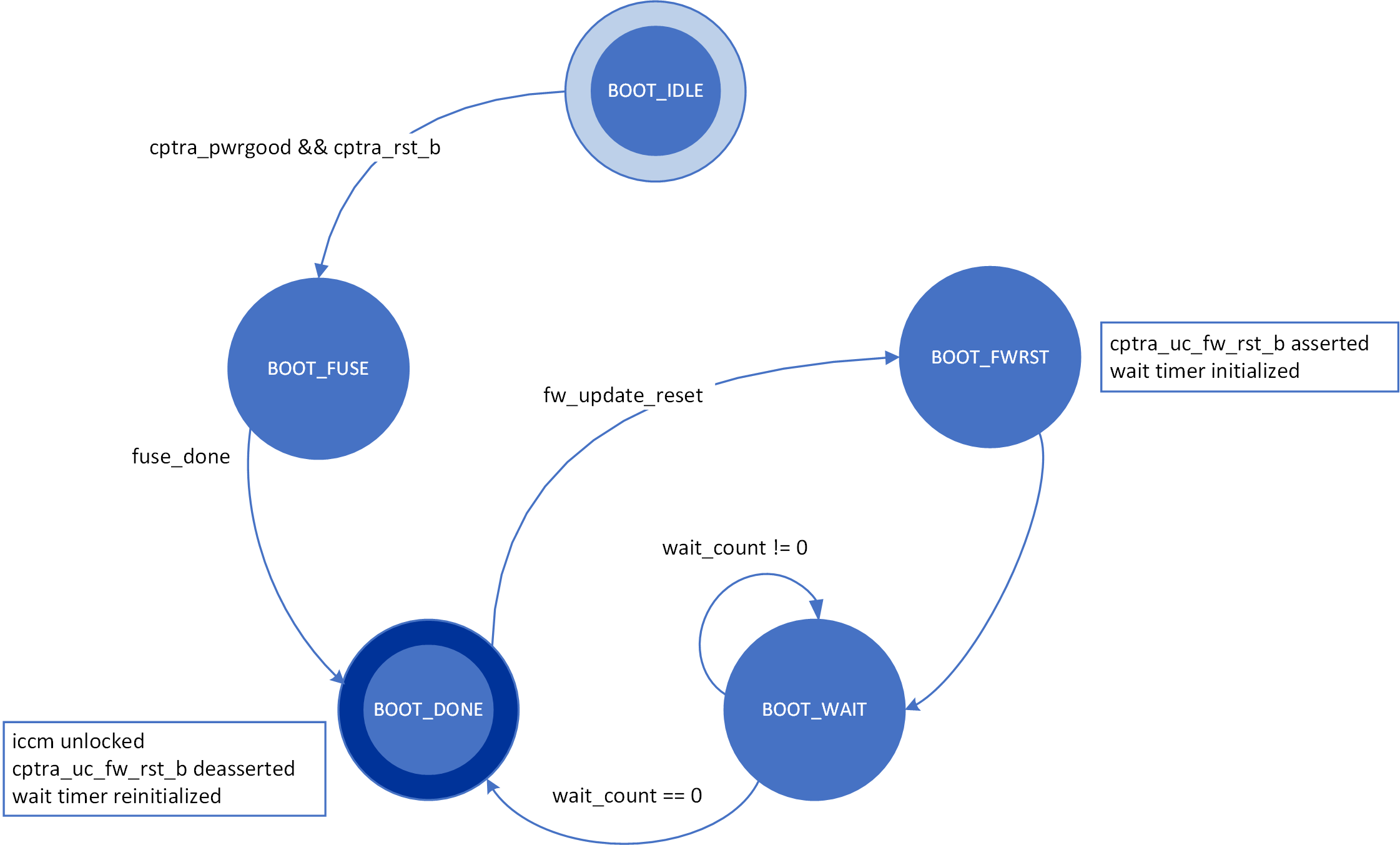
The boot FSM first waits for the SoC to assert cptra_pwrgood and deassert cptra_rst_b. The SoC should wait a minimum of 10 clocks after asserting cptra_pwrgood before deasserting cptra_rst_b. In the BOOT_FUSE state, Caliptra signals to the SoC that it is ready for fuses. After the SoC is done writing fuses, it sets the fuse done register and the FSM advances to BOOT_DONE.
BOOT_DONE enables Caliptra reset deassertion through a two flip-flop synchronizer.
SoC access mechanism
The SoC communicates with the mailbox through an APB Interface. The SoC acts as the requester with the Caliptra mailbox as the receiver.
The PAUSER bits are used by the SoC to identify which device is accessing the mailbox.
Mailbox
The Caliptra mailbox is a 128 KiB buffer used for exchanging data between the SoC and the Caliptra microcontroller.
When a mailbox is populated by the SoC, initiation of the operation by writing the execute bit triggers an interrupt to the microcontroller. This interrupt indicates that a command is available in the mailbox. The microcontroller is responsible for reading from and responding to the command.
When a mailbox is populated by the microcontroller, an output wire to the SoC indicates that a command is available in the mailbox. The SoC is responsible for reading from and responding to the command.
Mailboxes are generic data-passing structures with a specific protocol that defines legal operations. This protocol for writing to and reading from the mailbox is enforced in hardware as described in the Caliptra mailbox errors section. How the command and data are interpreted by the microcontroller and SoC are not enforced in this specification.
Sender Protocol
Sending data to the mailbox:
- Requester queries the mailbox by reading the LOCK control register.
- If LOCK returns 0, LOCK is granted and will be set to 1.
- If LOCK returns 1, MBOX is locked for another device.
- Requester writes the command to the COMMAND register.
- Requester writes the data length in bytes to the DLEN register.
- Requester writes data packets to the MBOX DATAIN register.
- Requester writes to the EXECUTE register.
- Requester reads the STATUS register. Status can return:
- CMD_BUSY - 2’b00 – Indicates the requested command is still in progress
- DATA_READY - 2’b01 – Indicates the return data is in the mailbox for requested command
- CMD_COMPLETE- 2’b10 – Indicates the successful completion of the requested command
- CMD_FAILURE- 2’b11 – Indicates the requested command failed
- Requester reads the response if DATA_READY was the status.
- Requester resets the EXECUTE register to release the lock.
Notes on behavior:
Once LOCK is granted, the mailbox is locked until that device has concluded its operation. Caliptra has access to an internal mechanism to terminate a lock early or release the lock if the device does not proceed to use it or to recover from deadlock scenarios. The following figure shows the sender protocol flow.
Figure 4: Sender protocol flow chart
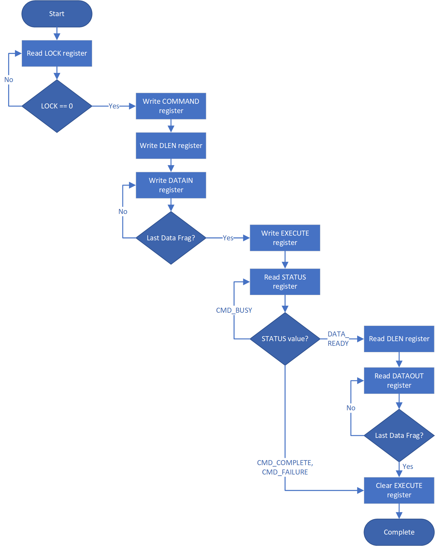
Receiver Protocol
Upon receiving indication that mailbox has been populated, the appropriate device can read the mailbox. This is indicated by a dedicated wire that is asserted when Caliptra populates the mailbox for SoC consumption.
Caliptra will not initiate any mailbox commands that require a response from the SoC. Caliptra initiated mailbox commands are “broadcast” and available to any user on the SoC. SoC will not be able to write the DLEN or DATAIN register while processing a Caliptra initiated mailbox command.
Receiving data from the mailbox:
- On mailbox_data_avail assertion, the receiver reads the COMMAND register.
- Receiver reads the DLEN register.
- Receiver reads the CMD register.
- Receiver reads the MBOX DATAOUT register.
- Continue reading MBOX DATAOUT register until DLEN bytes are read.
- If a response is required, the receiver can populate the mailbox with the response by updating the DLEN register and writing to DATAIN with the response. (NOTE: The new DLEN value will not take effect until control is returned to the sender via write to the status register).
- Set the mailbox status register appropriately to hand control back to the sender.
- The sender will reset the EXECUTE register.
- This releases the LOCK on the mailbox.
The following figure shows the receiver protocol flow.
Figure 5: Receiver protocol flowchart
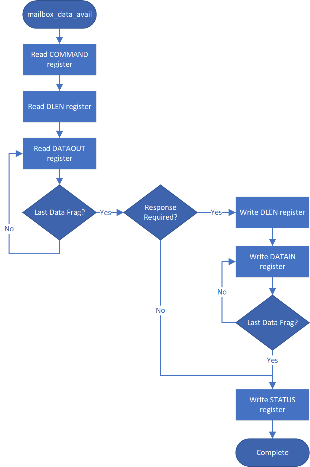
Mailbox arbitration
From a mailbox protocol perspective, as long as CPTRA_VALID_PAUSER registers carry valid requestors, mailbox lock can be obtained by any of those valid requestors but only one of them at any given time. While the mailbox flow is happening, all other requestors will not get a grant.
A request for lock that is denied due to firmware having the lock results in an interrupt to the firmware. Firmware can optionally use this interrupt to release the lock.
There is no fair arbitration scheme between SoC and microcontroller. It is first come, first served. When the mailbox is locked for microcontroller use and SoC has unsuccessfully requested the mailbox (due to mailbox actively being used), the mailbox generates an interrupt to the microcontroller as a notification.
Further, there is no arbitration between various PAUSER attributes. PAUSER attributes exist for security and filtering reasons only.
MAILBOX PAUSER attribute register
It is strongly recommended that these PAUSER registers are either set at integration time through integration parameters or be programmed by the SoC ROM before any mutable firmware or ROM patches are applied.
Programmable registers
Caliptra provides 5 programmable registers that SoC can set at boot time to limit access to the mailbox peripheral. The default PAUSER set by the integration parameter CPTRA_DEF_MBOX_VALID_PAUSER is valid at all times. CPTRA_MBOX_VALID_PAUSER registers become valid once the corresponding lock bit CPTRA_MBOX_PAUSER_LOCK is set.
Table 13: PAUSER register definition
| Register | Description |
|---|---|
| CPTRA_MBOX_VALID_PAUSER[4:0][31:0] | 5 registers for programming PAUSER values that are considered valid for accessing the mailbox protocol. Requests with PAUSER attributes that are not in this list will be ignored. |
| CPTRA_MBOX_PAUSER_LOCK[4:0] | 5 registers, bit 0 of each will lock and mark VALID for the corresponding VALID_PAUSER register. |
Parameter override
Another option for limiting access to the mailbox peripheral are the integration time parameters that override the programmable PAUSER registers. At integration time, the CPTRA_SET_MBOX_PAUSER_INTEG parameters can be set to 1 which enables the corresponding CPTRA_MBOX_VALID_PAUSER parameters to override the programmable register.
Table 14: PAUSER Parameter definition
| Parameter | Description |
|---|---|
| CPTRA_SET_MBOX_PAUSER_INTEG[4:0] | Setting to 1 enables the corresponding CPTRA_MBOX_VALID_PAUSER parameter. |
| CPTRA_MBOX_VALID_PAUSER[4:0] | Value to override programmable PAUSER register at integration time if corresponding CPTRA_SET_MBOX_PAUSER_INTEG parameter is set to 1. |
Caliptra mailbox protocol
After the SoC side has written the EXECUTE register, the mailbox sends an interrupt to the microcontroller.
The microcontroller reads the COMMAND and DLEN registers, as well as the data populated in the mailbox.
The microcontroller can signal back to SoC through functional registers, and populate COMMAND, DLEN, and MAILBOX as well.
Caliptra mailbox errors
Mailbox is responsible for only accepting writes from the device that requested and locked the mailbox.
If the SoC violates this protocol, the mailbox flags a protocol violation and enters an error state. Two protocol violations are detected:
- Access without lock: Writes to any mailbox register by SoC or reads from the dataout register, without having first acquired the lock, are a violation.
- If any agent currently has the lock, accesses by agents other than the one holding the lock are ignored.
- If no agent currently has the lock, the violation results in a flagged error.
- Out of order access: SoC must follow the rules for the sender and receiver protocol that define access ordering and progression for a mailbox command.
- If, after acquiring the lock, an SoC agent performs any register write (or read from the dataout register) outside of the prescribed ordering, this is a flagged violation.
- Such access by any SoC agent that does not have the lock is ignored.
After a mailbox protocol violation is flagged, it is reported to the system in several ways:
-
The mailbox FSM enters the ERROR state in response to an out of order access violation, and the new FSM state is readable via the mailbox status register. The LOCK value is preserved on entry to the ERROR state. The access without lock violation does not result in a state change. After entering the ERROR state, the mailbox may only be restored to the IDLE state by:
- System reset
- Write to the force unlock register by firmware inside Caliptra (via internal bus)
Either of these mechanisms will also clear the mailbox LOCK.
-
Mailbox protocol violations are reported as fields in the HW ERROR non-fatal register. These events also cause assertion of the cptra_error_non_fatal interrupt signal to SoC. Upon detection, SoC may acknowledge the error by clearing the error field in this register via bus write.
-
Mailbox protocol violations generate an internal interrupt to the Caliptra microcontroller. Caliptra firmware is aware of the protocol violation.
The following table describes APB transactions that cause the Mailbox FSM to enter the ERROR state, given that the register “mbox_user” contains the value of the APB PAUSER that was used to originally acquire the mailbox lock.
Table 15: Mailbox protocol error trigger conditions
| FSM state | SoC HAS LOCK | APB PAUSER eq mbox_user | Error state trigger condition |
|---|---|---|---|
| MBOX_RDY_FOR_CMD | 1 | true | Read from mbox_dataout. Write to any register other than mbox_cmd. |
| MBOX_RDY_FOR_CMD | 1 | false | - |
| MBOX_RDY_FOR_CMD | 0 | - | - |
| MBOX_RDY_FOR_DLEN | 1 | true | Read from mbox_dataout. Write to any register other than mbox_dlen. |
| MBOX_RDY_FOR_DLEN | 1 | false | - |
| MBOX_RDY_FOR_DLEN | 0 | - | - |
| MBOX_RDY_FOR_DATA | 1 | true | Read from mbox_dataout. Write to any register other than mbox_datain or mbox_execute. |
| MBOX_RDY_FOR_DATA | 1 | false | - |
| MBOX_RDY_FOR_DATA | 0 | - | - |
| MBOX_EXECUTE_UC | 1 | true | Read from mbox_dataout. Write to any register. |
| MBOX_EXECUTE_UC | 1 | false | - |
| MBOX_EXECUTE_UC | 0 | - | - |
| MBOX_EXECUTE_SOC | 1 | true | Write to any register other than mbox_execute. |
| MBOX_EXECUTE_SOC | 1 | false | - |
| MBOX_EXECUTE_SOC | 0 | true/false* | Write to any register other than mbox_status. |
* mbox_user value is not used when Caliptra has lock and is sending a Caliptra to SoC mailbox operation.
SoC SHA acceleration block
Overview
The SHA acceleration block is in the SoC interface. The SoC can access the accelerator’s hardware API and stream data to be hashed over the APB interface.
SHA acceleration block uses a similar protocol to the mailbox, but has its own dedicated registers.
SHA_LOCK register is set on read. A read of 0 indicates the SHA was unlocked and will now be locked for the requesting user.
SHA_MODE register sets the mode of operation for the SHA.
See the Hardware specification for additional details.
- 2’b00 - SHA384 streaming mode
- 2’b01 - SHA512 streaming mode
- 2’b10 - SHA384 mailbox mode (Caliptra only, invalid for SoC requests)
- 2’b11 - SHA512 mailbox mode (Caliptra only, invalid for SoC requests)
SoC Sender Protocol
Sending data to the SHA accelerator:
- Requester queries the accelerator by reading the SHA_LOCK control register.
- If SHA_LOCK returns 0, SHA_LOCK is granted and is set to 1.
- If SHA_LOCK returns 1, it is locked for another device.
- Requester writes the SHA_MODE register to the appropriate mode of operation.
- Requester writes the data length in bytes to the SHA_DLEN register.
- Requester writes data packets to the SHA_DATAIN register until SHA_DLEN bytes are written.
- Requester writes the SHA_EXECUTE register, this indicates that it is done streaming data.
- Requesters can poll the SHA_STATUS register for the VALID field to be asserted.
- Once VALID is asserted, the completed hash can be read from the SHA_DIGEST register.
- Requester must write 1 to the LOCK register to release the lock.
TRNG REQ HW API
For SoCs that choose to not instantiate Caliptra’s embedded TRNG, we provide a TRNQ REQ HW API.
While the use of this API is convenient for early enablement, the current Caliptra hardware is unable to provide the same security guarantees with an external TRNG. In particular, it is highly advisable to instantiate an internal TRNG if ROM glitch protection is important.
- Caliptra asserts TRNG_REQ wire (this may be because Caliptra’s internal hardware or firmware made the request for a TRNG).
- SoC writes the TRNG architectural registers.
- SoC write a done bit in the TRNG architectural registers.
- Caliptra deasserts TRNG_REQ.
Having an interface that is separate from the SoC mailbox ensures that this request is not intercepted by any SoC firmware agents (which communicate with SoC mailbox). It is a requirement for FIPS compliance that this TRNG HW API is always handled by SoC hardware gasket logic (and not some SoC ROM or firmware code).
TRNG DATA register is tied to TRNG VALID PAUSER. SoC can program the TRNG VALID PAUSER and lock the register using TRNG_PAUSER_LOCK[LOCK]. This ensures that TRNG DATA register is read-writeable by only the PAUSER programmed into the TRNG_VALID_PAUSER register. If the CPTRA_TNRG_PAUSER_LOCK.LOCK is set to ‘0, then any agent can write to the TRNG DATA register. If the lock is set, only an agent with a specific TRNG_VALID_PAUSER can write.
The ROM and firmware currently time out on the TRNG interface after 250,000 attempts to read a DONE bit. This bit is set in the architectural registers, as referenced in 3 in the preceding list.
SRAM implementation
Overview
SRAMs are instantiated at the SoC level. Caliptra provides the interface to export SRAMs from internal components.
SRAM repair logic (for example, BIST) and its associated fuses, which are proprietary to companies and their methodologies, is implemented external to the Caliptra boundary.
SRAMs must NOT go through BIST or repair flows across a “warm reset”. SoC shall perform SRAM repair during a powergood cycling event ("cold reset") and only prior to deasserting cptra_rst_b. During powergood cycling events, SoC shall also initialize all entries in the SRAM to a 0 value, prior to deasserting caliptra_rst_b.
Mailbox SRAM is implemented with ECC protection. Data width for the mailbox is 32-bits, with 7 parity bits for a Hamming-based SECDED (single-bit error correction and double-bit error detection).
RISC-V internal memory export
To support synthesis flexibility and ease memory integration to various fabrication processes, all SRAM blocks inside the RISC-V core are exported to an external location in the testbench. A single unified interface connects these memory blocks to their parent logic within the RISC-V core. Any memory implementation may be used to provide SRAM functionality in the external location in the testbench, provided the implementation adheres to the interface requirements connected to control logic inside the processor. Memories behind the interface are expected to be implemented as multiple banks of SRAM, from which the RISC-V processor selects the target using an enable vector. The I-Cache has multiple ways, each containing multiple banks of memory, but I-Cache is disabled in Caliptra and this may be removed for synthesis.
The following memories are exported:
- Instruction Closely-Coupled Memory (ICCM)
- Data Closely Coupled Memory (DCCM)
Table 4 indicates the signals contained in the memory interface. Direction is relative to the exported memory wrapper that is instantiated outside of the Caliptra subsystem (that is, from the testbench perspective).
SRAM timing behavior
- [Writes] Input wren signal is asserted simultaneously with input data and address. Input data is stored at the input address 1 clock cycle later.
- [Reads] Input clock enable signal is asserted simultaneously with input address. Output data is available 1 clock cycle later from a flip-flop register stage.
- [Writes] Input wren signal is asserted simultaneously with input data and address. Data is stored at the input address 1 clock cycle later.
The following figure shows the SRAM interface timing.
Figure 6: SRAM interface timing
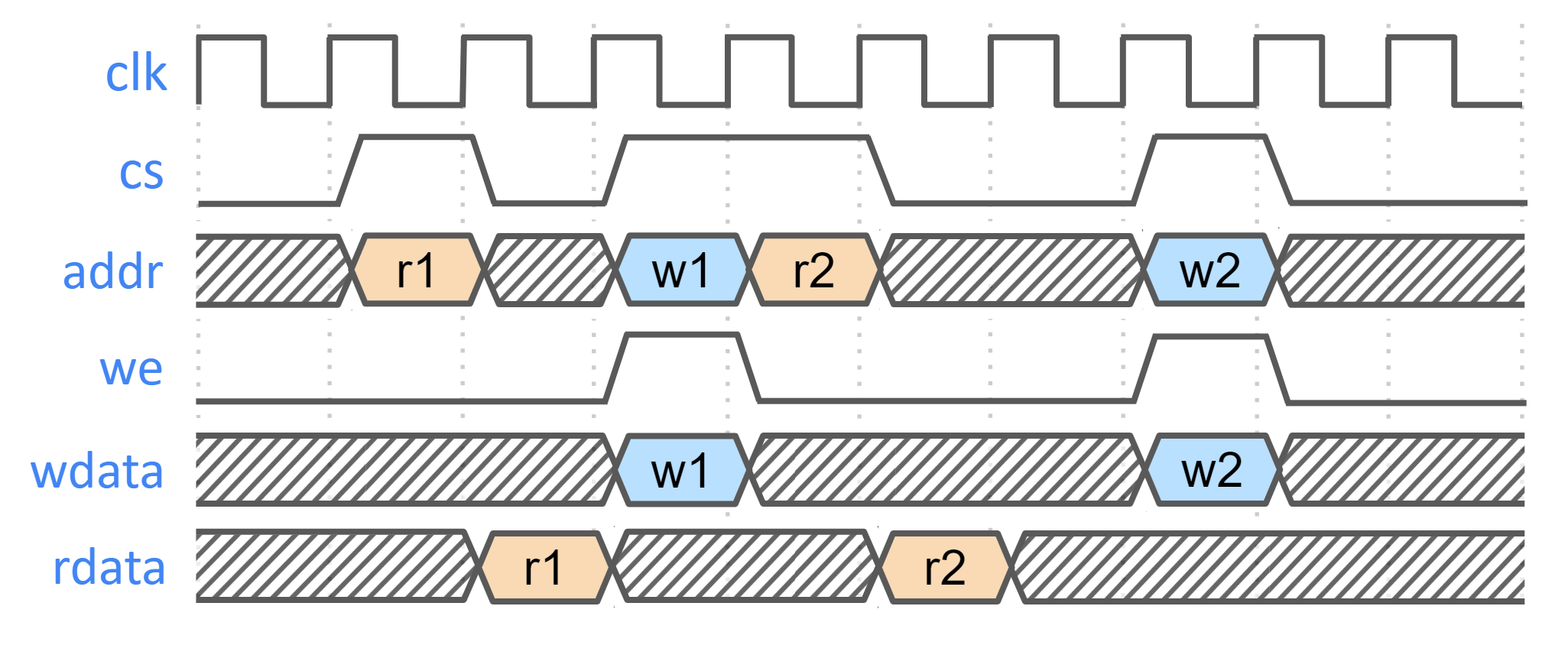
SRAM parameterization
Parameterization for ICCM/DCCM memories is derived from the configuration of the VeeR RISC-V core that has been selected for Caliptra integration. Parameters defined in the VeeR core determine signal dimensions at the Caliptra top-level interface and drive requirements for SRAM layout. For details about interface parameterization, see the Interface section. The following configuration options from the RISC-V Core dictate this behavior:
Table 16: SRAM parameterization
| Parameter | Value | Description |
|---|---|---|
| ICCM_ENABLE | 1 | Configures ICCM to be present in VeeR core. |
| ICCM_NUM_BANKS | 4 | Determines the number of physical 39-bit (32-bit data + 7-bit ECC) SRAM blocks that are instantiated in the ICCM. |
| ICCM_INDEX_BITS | 13 | Address bit width for each ICCM Bank that is instantiated. |
| ICCM_SIZE | 128 | Capacity of the ICCM in KiB. Total ICCM capacity in bytes is given by 4 * ICCM_NUM_BANKS * 2ICCM_INDEX_BITS. |
| DCCM_ENABLE | 1 | Configures DCCM to be present in VeeR core. |
| DCCM_NUM_BANKS | 4 | Determines the number of physical 39-bit (32-bit data + 7-bit ECC) SRAM blocks that are instantiated in the DCCM. |
| DCCM_INDEX_BITS | 13 | Address bit width for each DCCM Bank that is instantiated. |
| DCCM_SIZE | 128 | Capacity of the DCCM in KiB. Total DCCM capacity in bytes is given by 4 * DCCM_NUM_BANKS * 2DCCM_INDEX_BITS. |
Example SRAM machine check reliability integration
This section describes an example implementation of integrator machine check reliability.
This example is applicable to scenarios where an integrator may need control of or visibility into SRAM errors for purposes of reliability or functional safety. In such cases, integrators may introduce additional layers of error injection, detection, and correction logic surrounding SRAMs. The addition of such logic is transparent to the correct function of Caliptra, and removes integrator dependency on Caliptra for error logging or injection.
Note that the example assumes that data and ECC codes are in non-deterministic bit-position in the exposed SRAM interface bus. Accordingly, redundant correction coding is shown in the integrator level logic (i.e., integrator_ecc(calitpra_data, caliptra_ecc)). If the Caliptra data and ECC are deterministically separable at the Caliptra interface, the integrator would have discretion to store the ECC codes directly and calculate integrator ECC codes for the data alone.
Figure 7: Example machine check reliability implementation
Error detection and logging
- Caliptra IP shall interface to ECC protected memories.
- Caliptra IP calculates and applies its own ECC code, which produces a total of 39-bit data written to external or INTEGRATOR instantiated SRAMs.
- Each 39-bit bank memory internally calculates 8-bit ECC on a write and stores 47 bits of data with ECC into SRAM.
- On read access syndrome is calculated based on 39-bit data.
- If parity error is detected and syndrome is valid, then the error is deemed single-bit and correctable.
- If no parity error is detected but syndrome == 0 or the syndrome is invalid, the error is deemed uncorrectable.
- On both single and double errors, the read data is modified before being returned to Caliptra.
- Since single-bit errors shall be corrected through INTEGRATOR instantiated logic, Caliptra never sees single-bit errors from SRAM.
- Double-bit or uncorrectable errors would cause unpredictable data to be returned to Caliptra. Since this condition shall be detected and reported to MCRIP, there is no concern or expectation that Caliptra will operate correctly after a double error.
- On detection, single errors are reported as transparent to MCRIP, double errors are reported as fatal.
- Along with error severity, MCRIP logs physical location of the error.
- After MCRIP logs an error, it has a choice to send out in-band notification to an external agent.
- MCRIP logs can be queried by SoC software.
Error injection
- MCRIP supports two error injection modes: intrusive and non-intrusive.
- Intrusive error injection:
- Can force a single or double error to be injected, which would result in incorrect data to be returned on read access.
- The intrusive error injection mode is disabled in Production fused parts via Security State signal.
- Non-intrusive error injection:
- Allows external software to write into MCRIP error log registers.
- The non-intrusive error injection does not interfere with the operation of memories.
- The non-intrusive error injection is functional in Production fused parts.
Caliptra error and recovery flow
- Caliptra Stuck:
- SoC BC timeout mechanism with 300us timeout.
- Caliptra reports non-fatal error during boot flow:
- cptra_error_non_fatal is an output Caliptra signal, which shall be routed to SoC interrupt controller.
- SoC can look at the Caliptra non-fatal error register for error source.
- Assume Caliptra can report a non-fatal error at any time.
- SoC should monitor the error interrupt or check it before sending any mailbox command.
- In the event of a non-fatal error during boot (that is, prior to a ready for RT signal), SoC should enter recovery flow and attempt to boot again using alternate boot part/partition.
- If SoC sees that a non-fatal error has occurred AFTER receiving the ready for RT signal, SoC may attempt to recover Caliptra by executing the “Run Self-Test” mailbox command (not yet defined).
- If this command completes successfully, SoC may continue using Caliptra as before.
- If this command is unsuccessful, Caliptra is in an error state for the remainder of the current boot.
- Non-fatal ECC errors are never reported by Caliptra; SoC needs to monitor MCRIP for non-fatal Caliptra ECC errors.
- Caliptra reports fatal error during boot flow:
- cptra_error_fatal is an output Caliptra signal, which shall be routed to SoC interrupt controller.
- SoC can look at the Caliptra fatal error register for error source.
- Assume Caliptra can report a fatal error at any time.
- Fatal errors are generally hardware in nature. SoC may attempt to recover by full reset of the entire SoC, or can move on and know that Caliptra will be unavailable for the remainder of the current boot.
- We cannot assume that uncorrectable errors will be correctly detected by Caliptra, ECC fatal errors shall be reported by SoC MCRIP.
SoC integration requirements
The following table describes SoC integration requirements.
For additional information, see Caliptra assets and threats.
Table 17: SoC integration requirements
| Category | Requirement | Definition of done | Rationale |
|---|---|---|---|
| Obfuscation Key | SoC backend flows shall generate obfuscation key with appropriate NIST compliance as dictated in the Caliptra RoT specification. | Statement of conformance | Required by UDS and Field Entropy threat model |
| Obfuscation Key | If not driven through PUF, SoC backend flows shall ECO the obfuscation key before tapeout. | Statement of conformance | Required by UDS and Field Entropy threat model |
| Obfuscation Key | Rotation of the obfuscation key (if not driven through PUF) between silicon steppings of a given product (for example, A0 vs. B0 vs. PRQ stepping) is dependent on company-specific policies. | Statement of conformance | Required by UDS and Field Entropy threat model |
| Obfuscation Key | SoC backend flows should not insert obfuscation key flops into the scan chain. | Synthesis report | Required by UDS and Field Entropy threat model |
| Obfuscation Key | For defense in depth, it is strongly recommended that debofuscation key flops are not on the scan chain. Remove the following signals from the scan chain: cptra_scan_mode_Latched_d cptra_scan_mode_Latched_f field_storage.internal_obf_key | Statement of conformance | Caliptra HW threat model |
| Obfuscation Key | SoC shall ensure that obfuscation key is available (and wires are stable) before Caliptra reset is de-asserted. | Statement of conformance | Functionality and security |
| Obfuscation Key | SoC shall implement protections for obfuscation key generation logic and protect against debug/sw/scandump visibility. 1. Any flops outside of Caliptra that store obfuscation key or parts of the key should be excluded from scandump. 2. SoC shall ensure that the obfuscation key is sent only to Caliptra through HW wires, and it is not visible anywhere outside of Caliptra. | Statement of conformance | Required for Caliptra threat model |
| DFT | Before scan is enabled (separate signal that SoC implements on scan insertion), SoC shall set Caliptra's scan_mode indication to '1 to allow secrets/assets to be flushed. | Statement of conformance | Required by Caliptra threat model |
| DFT | Caliptra’s TAP should be a TAP endpoint. | Statement of conformance | Functional requirement |
| Mailbox | SoC shall provide an access path between the mailbox and the application CPU complex on SoCs with such complexes (for example, Host CPUs and Smart NICs). See the Sender Protocol section for details about error conditions. | Statement of conformance | Required for Project Kirkland and TDISP TSM |
| Fuses | SoC shall burn non-field fuses during manufacturing. Required vs. optional fuses are listed in the architectural specification. | Test on silicon | Required for UDS threat model |
| Fuses | SoC shall expose an interface for burning field fuses. Protection of this interface is the SoC vendor’s responsibility. | Test on silicon | Required for Field Entropy |
| Fuses | SoC shall write fuse registers and fuse done via immutable logic or ROM code. | Statement of conformance | Required for Caliptra threat model |
| Fuses | SoC shall expose an API for programming Field Entropy as described in the architecture documentation. SoC shall ensure that Field Entropy can only be programmed via this API and shall explicitly prohibit burning of discrete Field Entropy bits and re-burning of already burned Field Entropy entries. | Test on silicon | Required for Field Entropy |
| Fuses | SoC shall ensure that any debug read paths for fuses are disabled in PRODUCTION lifecycle state. | Test on silicon | Required for Field Entropy |
| Fuses | SoC shall ensure that UDS_SEED and Field Entropy supplied to Caliptra come directly from OTP fuses and there are no debug paths to inject new values. | Statement of conformance | Required for Caliptra threat model |
| Fuses | SoC shall add integrity checks for Caliptra fuses as per SoC policy. | Statement of conformance | Reliability |
| Fuses | SoC should apply shielding/obfuscation measures to protect fuse macro. | Statement of conformance | Required for Caliptra threat model |
| Fuses | SoCs that intend to undergo FIPS 140-3 zeroization shall expose zeroization API as described in zeroization requirements in architecture specification. SoC shall apply appropriate authentication for this API to protect against denial of service and side channel attacks. | Test on silicon | FIPS 140-3 certification |
| Security State | SoC shall drive security state wires in accordance with the SoC's security state. | Statement of conformance | Required for Caliptra threat model |
| Security State | If SoC is under debug, then SoC shall drive debug security state to Caliptra. | Statement of conformance | Required for Caliptra threat model |
| Resets and Clocks | SoC shall start input clock before caliptra_pwrgood assertion. | Statement of conformance | Functional |
| Resets and Clocks | SoC reset logic shall assume reset assertions are asynchronous and deassertions are synchronous. | Statement of conformance | Functional |
| Resets and Clocks | SoC shall ensure Caliptra's powergood is tied to SoC’s own powergood or any other reset that triggers SoC’s cold boot flow. | Statement of conformance | Required for Caliptra threat model |
| Resets and Clocks | SoC shall ensure Caliptra clock is derived from an on-die oscillator circuit. | Statement of conformance | Required for Caliptra threat model |
| Resets and Clocks | SoC shall ensure that any programmable Caliptra clock controls are restricted to the SoC Manager. | Statement of conformance | Required for Caliptra threat model |
| Resets and Clocks | SoC should defend against external clock stop attacks. | Statement of conformance | Required for Caliptra threat model |
| Resets and Clocks | SoC should defend against external clock glitching attacks. | Statement of conformance | Required for Caliptra threat model |
| Resets and Clocks | SoC should defend against external clock overclocking attacks. | Statement of conformance | Required for Caliptra threat model |
| TRNG | SoC shall either provision Caliptra with a dedicated TRNG or shared TRNG. It is highly recommended to use dedicated ITRNG | Statement of conformance | Required for Caliptra threat model and Functional |
| TRNG | SoC shall provision the Caliptra embedded TRNG with an entropy source if that is used (vs. SoC-shared TRNG API support). | Statement of conformance | Functional |
| TRNG | If the TRNG is shared, then upon TRNG_REQ, SoC shall use immutable logic or code to program Caliptra's TRNG registers. | Statement of conformance | Required for Caliptra threat model and Functional |
| SRAMs | SoC shall ensure timing convergence with 1-cycle read path for SRAMs. | Synthesis report | Functional |
| SRAMs | SoC shall size SRAMs to account for SECDED. | Statement of conformance | Functional |
| SRAMs | SoC shall write-protect fuses that characterize the SRAM. | Statement of conformance | Required for Caliptra threat model |
| SRAMs | SoC shall ensure SRAM content is only destroyed on powergood cycling. | Statement of conformance | Functional (Warm Reset, Hitless Update) |
| SRAMs | SoC shall only perform SRAM repair on powergood events and prior to caliptra_rst_b deassertion. SoC shall also ensure that SRAMs are initialized with all 0 data during powergood events, and prior to caliptra_rst_b deassertion. | Statement of conformance | Functional (Warm Reset, Hitless Update) |
| Backend convergence | Caliptra supports frequencies up to 400MHz using an industry standard, moderately advanced technology node as of 2023 September. | Statement of conformance | Functional |
| Power saving | Caliptra clock gating shall be controlled by Caliptra firmware alone. SoC is provided a global clock gating enable signal (and a register) to control. | Statement of conformance | Required for Caliptra threat model |
| Power saving | SoC shall not power-gate Caliptra independently of the entire SoC. | Statement of conformance | Required for Caliptra threat model |
| PAUSER | SoC shall drive PAUSER input in accordance with the IP integration spec. | Statement of conformance | Required for Caliptra threat model |
| Error reporting | SoC shall report Caliptra error outputs. | Statement of conformance | Telemetry and monitoring |
| Error reporting | SoC shall only recover Caliptra fatal errors via SoC power-good reset. | Statement of conformance | Required for Caliptra threat model |
| TRNG PAUSER Programming rules | If SoC doesn’t program the CPTRA_TRNG_PAUSER_LOCK[LOCK], then Caliptra HW will not accept TRNG data from any SoC entity. | Security | Required for Caliptra threat model |
| TRNG PAUSER Programming rules | If SoC programs CPTRA_TRNG_VALID_PAUSER and sets CPTRA_TRNG_PAUSER_LOCK[LOCK], then Caliptra HW will accept TRNG data only from the entity that is programmed into the PAUSER register. | Security | Required for Caliptra threat model |
| TRNG PAUSER Programming rules | It is strongly recommended that these PAUSER registers are either set at integration time through integration parameters or be programmed by the SoC ROM before any mutable FW or ROM patches are absorbed. | Security | Required for Caliptra threat model |
| MAILBOX PAUSER programming rules | 5 PAUSER attribute registers are implemented at SoC interface. | Security | Required for Caliptra threat model |
| MAILBOX PAUSER programming rules | At boot time, a default SoC or PAUSER can access the mailbox. The value of this PAUSER is an integration parameter, CPTRA_DEF_MBOX_VALID_PAUSER. | Security | Required for Caliptra threat model |
| MAILBOX PAUSER programming rules | The value of CPTRA_MBOX_VALID_PAUSER[4:0] register can be programmed by SoC. After it is locked, it becomes a valid PAUSER for accessing the mailbox. | Security | Required for Caliptra threat model |
| MAILBOX PAUSER programming rules | CPTRA_SET_MBOX_PAUSER_INTEG parameter can be set along with the corresponding CPTRA_MBOX_VALID_PAUSER parameter at integration time. If set, these integration parameters take precedence over the CPTRA_MBOX_VALID_PAUSER[4:0] register. | Security | Required for Caliptra threat model |
| MAILBOX PAUSER programming rules | SoC logic (ROM, HW) that is using the Caliptra mailbox right out of cold reset, without first configuring the programmable mailbox PAUSER registers, must send the mailbox accesses with the default PAUSER, CPTRA_DEF_MBOX_VALID_PAUSER. | Security | Required for Caliptra threat model |
| MAILBOX PAUSER programming rules | For CPTRA_MBOX_VALID_PAUSER[4:0], the corresponding lock bits MUST be programmed to ‘1. This enables the mailbox to accept transactions from non-default PAUSERS. | Security | Required for Caliptra threat model |
| MAILBOX PAUSER programming rules | It is strongly recommended that mailbox PAUSER registers are either set at integration time through integration parameters or are programmed by the SoC ROM before any mutable FW or ROM patches are applied. | Security | Required for Caliptra threat model |
| FUSE PAUSER programming rules | 1 PAUSER attribute register is implemented at SoC interface: CPTRA_FUSE_VALID_PAUSER. | Security | Required for Caliptra threat model |
| FUSE PAUSER programming rules | CPTRA_FUSE_PAUSER_LOCK locks the programmable valid pauser register, and marks the programmed value as valid. | Security | Required for Caliptra threat model |
| FUSE PAUSER programming rules | Integrators can choose to harden the valid pauser for fuse access by setting the integration parameter, CPTRA_FUSE_VALID_PAUSER, to the desired value in RTL, and by setting CPTRA_SET_FUSE_PAUSER_INTEG to 1. If set, these integration parameters take precedence over the CPTRA_FUSE_VALID_PAUSER register. | Security | Required for Caliptra threat model |
| Manufacturing | SoC shall provision an IDevID certificate with fields that conform to the requirements described in Provisioning IDevID during manufacturing. | Statement of conformance | Functionality |
| Manufacturing | Caliptra relies on obfuscation for confidentiality of UDS_SEED. It is strongly advised to implement manufacturing policies to protect UDS_SEED as defense in depth measures. 1, Prevent leakage of UDS_SEED on manufacturing floor. 2. Implement policies to prevent cloning (programming same UDS_SEED into multiple devices). 3. Implement policies to prevent signing of spurious IDEVID certs. | Statement of conformance | Required for Caliptra threat model |
| Chain of trust | SoC shall ensure all mutable code and configuration measurements are stashed into Caliptra. A statement of conformance lists what is considered mutable code and configuration vs. what is not. The statement also describes the start of the boot sequence of the SoC and how Caliptra is incorporated into it. | Statement of conformance | Required for Caliptra threat model |
| Chain of trust | SoC shall limit the mutable code and configuration that persists across the Caliptra powergood reset. A statement of conformance lists what persists and why this persistence is necessary. | Statement of conformance | Required for Caliptra threat model |
| Implementation | SoC shall apply size-only constraints on cells tagged with the "u__size_only__" string and shall ensure that these are not optimized in synthesis and PNR | Statement of conformance | Required for Caliptra threat model |
| GLS FEV | GLS FEV must be run to make sure netlist and RTL match and none of the countermeasures are optimized away. See the following table for example warnings from synthesis runs to resolve through FEV | GLS simulations pass | Functional requirement |
Table 18: Caliptra synthesis warnings for FEV evaluation
| Module | Warning | Line No. | Description |
|---|---|---|---|
| sha512_acc_top | Empty netlist for always_comb | 417 | Unused logic (no load) |
| ecc_scalar_blinding | Netlist for always_ff block does not contain flip flop | 301 | Output width is smaller than internal signals, synthesis optimizes away the extra internal flops with no loads |
| sha512_masked_core | "masked_carry" is read before being assigned. Synthesized result may not match simulation | 295, 312 | |
| ecc_montgomerymultiplier | Netlist for always_ff block does not contain flip flop | 274, 326 | Output width is smaller than internal signals, synthesis optimizes away the extra internal flops with no loads |
| Multiple modules | Signed to unsigned conversion occurs |
Integrator RTL modification requirements
Several files contain code that may be specific to an integrator's implementation and should be overridden. This overridable code is either configuration parameters with integrator-specific values or modules that implement process-specific functionality. Code in these files should be modified or replaced by integrators using components from the cell library of their fabrication vendor. The following table describes recommended modifications for each file.
Table 19: Caliptra integrator custom RTL file list
| File | Description |
|---|---|
| config_defines.svh | Enable Caliptra internal TRNG (if applicable). Declare name of custom clock gate module by defining USER_ICG. Enable custom clock gate by defining TECH_SPECIFIC_ICG. |
| soc_ifc_pkg.sv | Define PAUSER default behavior and (if applicable) override values. See Integration Parameters. |
| caliptra_icg.sv | Replace with a technology-specific clock gater. Modifying this file is not necessary if integrators override the clock gate module that is used by setting TECH_SPECIFIC_ICG. |
| beh_lib.sv | Replace rvclkhdr/rvoclkhdr with a technology-specific clock gater. Modifying this file may not be necessary if integrators override the clock gate module that is used by setting TECH_SPECIFIC_EC_RV_ICG. |
| beh_lib.sv | Replace rvsyncss (and rvsyncss_fpga if the design will be implemented on an FPGA) with a technology-specific sync cell. |
| caliptra_prim_flop_2sync.sv | Replace with a technology-specific sync cell. |
| caliptra_2ff_sync.sv | Replace with a technology-specific sync cell. |
| dmi_jtag_to_core_sync.v | Replace with a technology-specific sync cell. This synchronizer implements edge detection logic using a delayed flip flop on the output domain to produce a pulse output. Integrators must take care to ensure logical equivalence when replacing this logic with custom cells. |
CDC analysis and constraints
Clock Domain Crossing (CDC) analysis is performed on the Caliptra core IP. The following are the results and recommended constraints for Caliptra integrators using standard CDC analysis EDA tools.
In an unconstrained environment, several CDC violations are anticipated. CDC analysis requires the addition of constraints to identify valid synchronization mechanisms and/or static/pseudo-static signals.
Analysis of missing synchronizers
- All of the signals, whether single-bit or multi-bit, originate from the rvjtag_tap module internal register on TCK clock, and the Sink/Endpoint is the rvdff register, which is in CalitpraClockDomain clock.
- JTAG does a series of “jtag writes” for each single “register write”.
- We only need to synchronize the controlling signal for this interface.
- Inside the dmi_wrapper, the dmi_reg_en and dmi_reg_wr_en comes from dmi_jtag_to_core_sync, which is a 2FF synchronizer.
The following code snippet and schematic diagram illustrate JTAG originating CDC violations.
Figure 8: Schematic diagram and code snippet showing JTAG-originating CDC violations
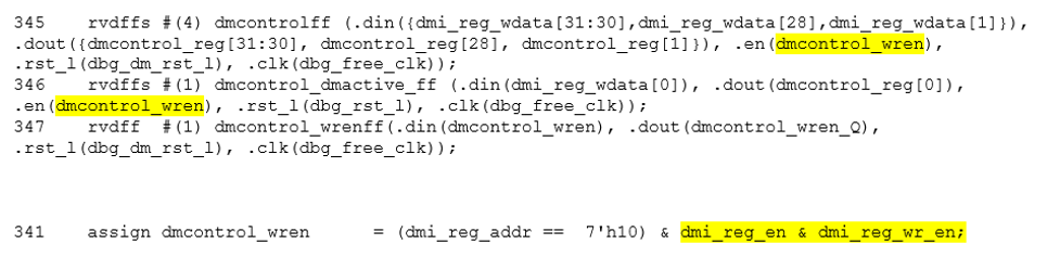
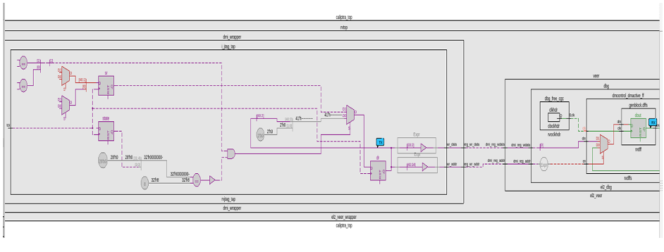
CDC analysis conclusions
- Missing synchronizers appear to be the result of “inferred” and/or only 2-FF instantiated synchronizers.
- dmi_jtag_to_core_sync.v contains inferred 2FF synchronizers on the control signals “dmi_reg_wr_en” and “dmi_reg_rd_en”.
- 2FF synchronizer inferences are considered non-compliant and should be replaced by an explicitly instantiated synchronization module, which is intended to be substituted on a per-integrator basis.
- cdc report scheme two_dff -severity violation
- Multi-bit signals are effectively pseudo-static and are qualified by synchronized control qualifiers.
- Pseudo-static: wr_data, wr_addr
- cdc signal reg_wr_data -module dmi_wrapper -stable
- cdc signal reg_wr_addr -module dmi_wrapper -stable
- Pseudo-static: wr_data, wr_addr
- The core clock frequency must be at least twice the TCK clock frequency for the JTAG data to pass correctly through the synchronizers.
CDC constraints
- cdc report scheme two_dff -severity violation
- cdc signal reg_wr_data -module dmi_wrapper -stable
- cdc signal reg_wr_addr -module dmi_wrapper -stable
- cdc signal rd_data -module dmi_wrapper -stable
RDC analysis and constraints
Reset Domain Crossing (RDC) analysis is performed on the Caliptra core IP. The following are the results and recommended constraints for Caliptra integrators using standard RDC analysis EDA tools.
In an unconstrained environment, several RDC violations are anticipated. RDC analysis requires the addition of constraints to identify valid synchronization mechanisms from one reset domain to another.
Constraining reset domains
Reset domains
The following table identifies the major reset domains in Caliptra core IP design.
Table 20: Reset definitions (functional resets are marked in bold)
| Reset name | Reset type | Reset polarity | Definition point | Reset generated by |
|---|---|---|---|---|
| CPTRA_PWRGD | Async | Active Low | cptra_pwrgood | Primary Input |
| CPTRA_RST | Async | Active Low | cptra_rst_b | Primary Input |
| CPTRA_UC_RST | Async | Active Low | caliptra_top.soc_ifc_top1.i_soc_ifc_boot_fsm.cptra_uc_rst_b | Generated by Boot FSM |
| CPTRA_NON_CORE_RST | Async | Active Low | caliptra_top.soc_ifc_top1.i_soc_ifc_boot_fsm.cptra_noncore_rst_b | Generated by Boot FSM |
| RISCV_VEER_CORE_RST | Async | Active Low | caliptra_top.rvtop.veer.core_rst_l | AND of BOOT_FSM_CPTRA_UC_RST and RISCV_VEER_DBG_CORE_RST Functionally same as CPTRA_UC_RST |
| RISCV_VEER_DBG_DM_RST | Async | Active Low | caliptra_top.rvtop.veer.dbg.dbg_dm_rst_l | AND of CPTRA_PWRGD and a bit controlled from JTAG TAP Functionally same as CPTRA_PWRGD |
| CPTRA_JTAG_RST | Async | Active Low | jtag_trst_n | Primary Input |
Reset structure
The reset definitions can be visually represented as shown in the following diagram.
Figure 9: Reset tree for Caliptra
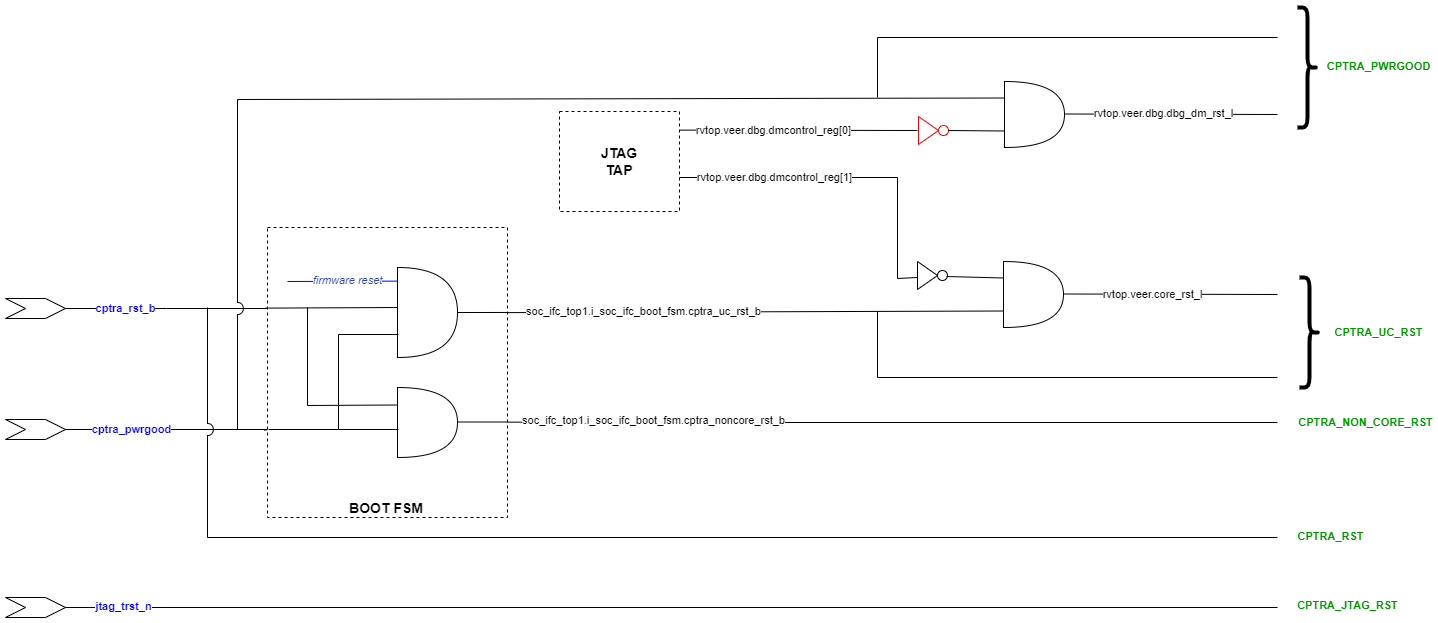
RDC false paths
The following table shows the false paths between various reset groups.
Table 21: Reset domain crossing false paths
| Launch flop reset | Capture flop reset | Comment |
|---|---|---|
| CPTRA_PWRGD | all other groups | CPTRA_PWRGD is the deepest reset domain, so all RDC paths from CPTRA_PWRGD can be set as false paths |
| CPTRA_RST | CPTRA_UC_RST | Boot FSM is reset by CPTRA_RST |
| CPTRA_RST | CPTRA_NON_CORE_RST | Boot FSM is reset by CPTRA_RST |
| CPTRA_NON_CORE_RST | CPTRA_RST | CPTRA_NON_CORE_RST can be asserted only by asserting CPTRA_RST |
| CPTRA_NON_CORE_RST | CPTRA_UC_RST | CPTRA_NON_CORE_RST can be asserted only by asserting CPTRA_RST Asserting CPTRA_RST means CPTRA_UC_RST will be asserted |
Reset sequencing scenarios
The resets defined in Table 20 have the following sequencing phases, which are applicable for different reset scenarios: cold boot, cold reset, warm reset and firmware reset.
The reset sequencing is illustrated in the following waveform.
Figure 10: Reset sequencing waveform for Caliptra
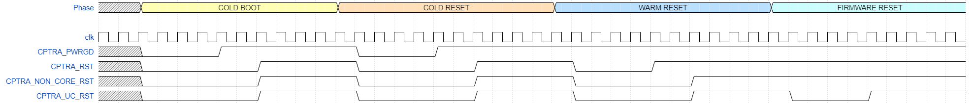
Reset ordering
The following table defines the order in which resets can get asserted. A ">>" in a cell at row X and column Y indicates that if the reset in row X is asserted, the reset in row Y is also asserted. For rest of the cells (in which symbol ">>" is not present) the preceding assumption is not true and so the paths between those resets are potential RDC violations. The black cells are ignored because they are between the same resets.
Table 22: Reset sequence ordering constraints
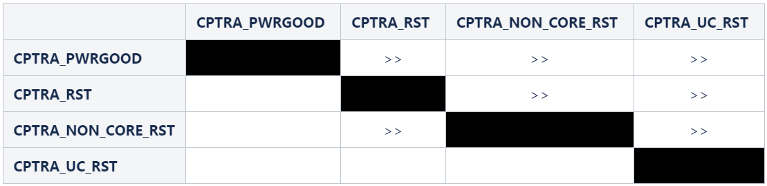
Reset constraints and assumptions
The following set of constraints and assumptions must be provided before running RDC structural analysis of Caliptra Core IP.
- Caliptra Core IP assumes the primary reset inputs are already synchronized to their respective clocks. The integrator must add external reset synchronizers to achieve the same.
- cptra_pwrgood and cptra_rst_b resets must be synchronized to cptra_clk
- Deassertion of jtag_trst_n reset must be synchronized to jtag_clk. The signal can be asserted asynchronously.
- The following debug register, which is driven from JTAG, is not toggled during functional flow.
- u_caliptra.rvtop.veer.dbg.dmcontrol_reg[0] = 0
- Set scan_mode to 0 for functional analysis.
- Stamp or create functional resets for cptra_noncore_rst_b and cptra_uc_rst_b at the definition points, as mentioned in Table 20.
- Create funtional reset grouping - This step must be customized as per the EDA tool, which is being used for RDC analysis. The goal of this customization is to achieve the following three sequencing requirements/constraints.
- Gate all clocks when cptra_noncore_rst_b is asserted. This ensures that the capture flop clock is gated while the source flop's reset is getting asserted, thereby preventing the capture flop from becoming metastable. The result is when cptra_noncore_rst_b is going to be asserted, the following signals are constrained to be at 1 at around that time.
- soc_ifc_top1.i_soc_ifc_boot_fsm.rdc_clk_dis
- soc_ifc_top1.i_soc_ifc_boot_fsm.arc_IDLE
- Gate Veer core clock when cptra_uc_rst_b is asserted. This ensures that the capture flop clock is gated while the source flop's reset is getting asserted, thereby preventing the capture flop from becoming metastable. The result is when cptra_uc_rst_b is going to be asserted, the following signal is constrained to be at 1 at around that time.
- soc_ifc_top1.i_soc_ifc_boot_fsm.fw_update_rst_window
- Quiesce the AHB bus before cptra_uc_rst_b is asserted. Since the firmware reset request is triggered by software, it can ensure that all AHB transcations are flushed out before initiating a reset request. This is done by generating a signal, fw_update_rst_window, which is asserted (driven to 1) around the firmware reset assertion edge. When fw_update_rst_window is asserted, the force_bus_idle signal of the AHB decoder is driven to 1, which ensures that all AHB requestes are driven low. So when cptra_uc_rst_b is going to get asserted, the following signals are constrained to be at 0 at around that time.
- doe.doe_inst.i_doe_reg.s_cpuif_req
- ecc_top1.ecc_reg1.s_cpuif_req
- hmac.hmac_inst.i_hmac_reg.s_cpuif_req
- key_vault1.kv_reg1.s_cpuif_req
- pcr_vault1.pv_reg1.s_cpuif_req
- data_vault1.dv_reg1.s_cpuif_req
- sha512.sha512_inst.i_sha512_reg.s_cpuif_req
- soc_ifc_top1.i_ahb_slv_sif_soc_ifc.dv
- sha256.sha256_inst.i_sha256_reg.s_cpuif_req
- csrng.u_reg.u_ahb_slv_sif.dv
- entropy_src.u_reg.u_ahb_slv_sif.dv
- Gate all clocks when cptra_noncore_rst_b is asserted. This ensures that the capture flop clock is gated while the source flop's reset is getting asserted, thereby preventing the capture flop from becoming metastable. The result is when cptra_noncore_rst_b is going to be asserted, the following signals are constrained to be at 1 at around that time.
- Constrain the RDC false paths as per Table 21.
RDC violations and waivers
Considering the given constraints, three sets of crossings were identified as RDC violations. All of them can be waived as explained in Table 23. Note that the report may differ across EDA tools due to variations in structural analysis, which can be influenced by a range of settings.
Table 23: Reset domain crossing violations
| Sl no | Launch reset | Launch flop | Capture reset | Capture flop |
|---|---|---|---|---|
| 1 | cptra_uc_rst_b | rvtop.veer.dec.tlu.exthaltff.genblock.dff.dout[7] | cptra_noncore_rst_b | cg.user_soc_ifc_icg.clk_slcg_0_generated_icg.p_clkgate.vudpi0.q |
| 2 | cptra_uc_rst_b | rvtop.veer.dec.tlu.exthaltff.genblock.dff.dout[7] | cptra_noncore_rst_b | cg.user_icg.clk_slcg_0_generated_icg.p_clkgate.vudpi0.q |
| 3 | cptra_uc_rst_b | rvtop.veer.Gen_AXI_To_AHB.lsu_axi4_to_ahb* | cptra_noncore_rst_b | entropy_src.u_entropy_src_core.u_caliptra_prim_packer_fifo_bypass.data_q* |
| 4 | cptra_uc_rst_b | rvtop.veer.Gen_AXI_To_AHB.lsu_axi4_to_ahb* | cptra_noncore_rst_b | entropy_src.u_entropy_src_core.u_caliptra_prim_packer_fifo_precon.data_q* |
For violations in Sl No 1 and 2, the schematic for the crossing is shown in the following figure.
Figure 11: Schematic for RDC violations #1 and #2
This violation can be waived because if the CPU is halted, there is no way to trigger a firmware update reset as it is initiated by the microcontroller itself. Thus, it can be ensured that on cptra_uc_rst_b, cpu_halt_status will be at the reset value already, which in turn ensures that there are no glitches on the output clock of CG.
For violations in Sl No 3 and 4, the schematic for the crossing is shown in the following figure.
Figure 12: Schematic for RDC violations #3 and #4
In the preceding schematic, an RDC crossing violation is identified at the data_q flop, which is located on the right-hand side of the figure. The analysis for prim_packer_fifo_bypass is elaborated here, with the same scenario applying to prim_packer_fifo_recon.
The fifo load and wr_data equations are as follows:
assign pfifo_bypass_push = !es_bypass_mode ? 1'b0 : fw_ov_mode_entropy_insert ? fw_ov_fifo_wr_pulse : pfifo_postht_not_empty; assign pfifo_bypass_wdata = fw_ov_mode_entropy_insert ? fw_ov_wr_data : pfifo_postht_rdata;The following scenarios can occur.
Table 24: Reset domain crossing scenarios for #3 and #4 crossing
| #Case | es_bypass_mode | fw_ov_mode_entropy_insert | pfifo_bypass_push | pfifo_bypass_wdata | Comment |
|---|---|---|---|---|---|
| 1 | 0 | don't care | 0 | don't care | No RDC violations, since the recirculation mux on data_q (pink on lower right side) prevents the flop from loading. |
| 2 | 1 | 0 | pfifo_postht_rdata | pfifo_postht_rdata | No RDC violations, since recirculation mux switches to the leg that is on the same reset domain (shown in purple on left side) |
| 3 | 0 | 1 | fw_ov_fifo_wr_pulse | fw_ov_wr_data | RDC violations are suppressed because fw_ov_fifo_wr_pulse = 0 (the red data lines on cptra_uc_rst_b are not able to reach data_q because load_data is 0) |
Referring to the preceding table, if it can be ensured that fw_ov_fifo_wr_pulse is 0 when cptra_uc_rst_b is asserted, RDC crossings (Case #3) can be avoided. This condition is described in the preceding Constraints section.
Synthesis findings
Synthesis experiments have so far found the following:
- Design converges at 400MHz 0.72V using an industry standard, moderately advanced technology node as of 2023 September.
- Design converges at 100MHz using TSMC 40nm process.
Note: Any synthesis warnings of logic optimization must be reviewed and accounted for.
Netlist synthesis data
The following table illustrates representative netlist synthesis results using industry standard EDA synthesis tools and tool configurations.
These metrics are inclusive of VeeR core, Caliptra logic, imem/dmem RAM, ROM.
The area is expressed in units of square microns.
The target foundry technology node is an industry standard, moderately advanced technology node as of 2024 June.
Table 25: Netlist synthesis data
| IP Name | Date | Path Group | Target Freq | QoR WNS | QoR Achieveable Freq |
|---|---|---|---|---|---|
| CALIPTRA_WRAPPER | 6/11/2024 | CALIPTRACLK | 500MHz | -0.09 | 500MHz |
| CALIPTRA_WRAPPER | 6/11/2024 | JTAG_TCK | 100MHz | 4606.5 | 100MHz |
| CALIPTRA_WRAPPER | 6/11/2024 | clock_gating_default | 500MHz | 3.36 | 500MHz |
| CALIPTRA_WRAPPER | 6/11/2024 | io_to_flop | 500MHz | 429.8 | 500MHz |
| CALIPTRA_WRAPPER | 6/11/2024 | flop_to_io | 500MHz | 0.10 | 500MHz |
| IP Name | Date | Stdcell Area | Macro Area | Memory Area | Total Area | Flop Count | No Clock Regs/Pins Count | FM Status | FM Eqv Pts | FM Non-Eqv Pts | FM Abort Pts | FM FM Non-Comp Pts |
|---|---|---|---|---|---|---|---|---|---|---|---|---|
| CALIPTRA_WRAPPER | 6/11/2024 | 93916 | 0 | 239937 | 341725 | 164505 | 0 | SUCCEEDED | 166241 | 0 | 0 | 0 |
Recommended LINT rules
A standardized set of lint rules is used to sign off on each release. The lint policy may be provided directly to integrators upon request to ensure lint is clean in the SoC.
Terminology
The following terminology is used in this document.
Table 26: Terminology
| Abbreviation | Description |
|---|---|
| AHB | AMBA Advanced High-Performance Bus |
| APB | AMBA Advanced Peripheral Bus |
| AES | Advanced Encryption Standard |
| BMD | Boot Media Dependent |
| BMI | Boot Media Integrated |
| ECC | Elliptic Curve Cryptography |
| ECO | Engineering Change Order (used to implement logic changes to a hardware design post-synthesis) |
| QSPI | Quad Serial Peripheral Interface |
| RISC | Reduced Instruction Set Computer |
| SHA | Secure Hashing Algorithm |
| SPI | Serial Peripheral Interface |
| UART | Universal Asynchronous Receiver Transmitter |
Core Registers
Redirecting to external documentation...
Click here if not redirected ↗
51ff0a8
Caliptra - ROM Specification v1.0
Scope
Caliptra is an open-source Hardware Root of Trust for Measurement (RTM). This document is the architecture specification for Caliptra Read Only Memory Code (ROM). As an architecture specification for ROM, this document describes the following topics:
-
Provide high level architecture and requirements
-
Describe ROM DICE Layering Architecture
-
Describe ROM functionality
-
Define ROM boot flows
- Cold Reset Flow
- Warm Reset Flow
- Update Reset Flow
- Unknown/Spurious Reset Flow
-
Cryptographic Derivations
Glossary
| Term | Description |
|---|---|
| CDI | Compound Device Identity |
| CSR | Certificate Signing Request |
| DCCM | Data Closely Coupled Memory |
| DICE | Device Identifier Composition Engine |
| FHT | Firmware Handoff Table |
| FMC | First Mutable Code |
| FW | Firmware |
| ICCM | Instruction Closely Coupled Memory |
| IDEVID | Initial Device ID DICE Layer |
| RoT | Root of Trust |
| RT | Runtime |
| RTM | Root of Trust for Measurement |
| TCI | Trusted Component Identifier |
| UDS | Unique Device Secret |
| SVN | Security Version Number |
| X509 | Digital Certificate Standard |
Fuse and architectural registers
Following are the main FUSE & Architectural Registers used by the Caliptra ROM for DICE Derivations:
| Register | Width (bits) | Description |
|---|---|---|
| CPTRA_SECURITY_STATE | 32 | Security State of the device. Contains two fields: LIFECYCLE_STATE: Unprovisioned, Manufacturing or Production DEBUG_ENABLED: Boolean indicating if debug is enabled or not |
| FUSE_UDS_SEED | 384 | Obfuscated UDS |
| FUSE_FIELD_ENTROPY | 384 | Obfuscated Field Entropy |
| FUSE_KEY_MANIFEST_PK_HASH | 384 | Hash of the four ECC and thirty-two LMS Manufacturer Public Keys |
| FUSE_KEY_MANIFEST_PK_HASH_MASK | 32 | Manufacturer ECC Public Key Revocation Mask |
| FUSE_LMS_REVOCATION | 32 | Manufacturer LMS Public Key Revocation Mask |
| FUSE_LMS_VERIFY | 32 | LMS Verification flag: 0 - Verify Caliptra firmware images with ECDSA-only 1 - Verify Caliptra firmware images with both ECDSA and LMS |
| FUSE_OWNER_PK_HASH | 384 | Owner ECC and LMS Public Key Hash |
| FUSE_FMC_KEY_MANIFEST_SVN | 32 | FMC Security Version Number |
| FUSE_RUNTIME_SVN | 128 | Runtime Security Version Number |
| FUSE_ANTI_ROLLBACK_DISABLE | 1 | Disable SVN checking for FMC & Runtime when bit is set |
| FUSE_IDEVID_CERT_ATTR | 768 | FUSE containing information for generating IDEVID CSR Word 0: X509 Key Id Algorithm (2 bits) 1: SHA1, 2: SHA256, 2: SHA384, 3: Fuse Word 1,2,3,4,5: Subject Key Id Words 7,8: Unique Endpoint ID |
| CPTRA_DBG_MANUF_SERVICE_REG | 16 | Manufacturing Services: Bit 0: IDEVID CSR upload Bit 1: Random Number Generator Unavailable Bit 15:8: FIPS test hook code Bit 30: Fake ROM enable in production lifecycle mode Bit 31: Fake ROM image verify enable |
Firmware image bundle
The Caliptra Firmware image has two main components:
The firmware manifest is a combination of preamble and a signed header. It has public keys, signatures and table of contents which refer to the various firmware images contained in the bundle.

Firmware manifest
Firmware manifest consists of preamble, header and table of contents.
Preamble
It is the unsigned portion of the manifest. Preamble contains the signing public keys and signatures. ROM is responsible for parsing the preamble. ROM performs the following steps:
- Loads the preamble from the mailbox.
- Calculates the hash of the four Manufacturer ECC and thirty-two LMS (if LMS verification is enabled) Public Keys in the preamble and compares it against the hash in the fuse (FUSE_KEY_MANIFEST_PK_HASH). If the hashes do not match, the boot fails.
- Selects the appropriate Manufacturer Public Key(s) based on fuse (FUSE_KEY_MANIFEST_PK_HASH_MASK for ECC public key, FUSE_LMS_REVOCATION for LMS public key)
Note: All fields are little endian unless specified
| Field | Size (bytes) | Description |
|---|---|---|
| Firmware Manifest Marker | 4 | Magic Number marking the start of the package manifest. The value must be 0x434D414E (‘CMAN’ in ASCII) |
| Firmware Manifest Size | 4 | Size of the full manifest structure |
| Manufacturer ECC Public Key 1 | 96 | ECC P-384 public key used to verify the Firmware Manifest Header Signature. X-Coordinate: Public Key X-Coordinate (48 bytes) Y-Coordinate: Public Key Y-Coordinate (48 bytes) |
| Manufacturer ECC Public Key 2 | 96 | ECC P-384 public key used to verify the Firmware Manifest Header Signature. X-Coordinate: Public Key X-Coordinate (48 bytes) Y-Coordinate: Public Key Y-Coordinate (48 bytes) |
| Manufacturer ECC Public Key 3 | 96 | ECC P-384 public key used to verify the Firmware Manifest Header Signature. X-Coordinate: Public Key X-Coordinate (48 bytes) Y-Coordinate: Public Key Y-Coordinate (48 bytes) |
| Manufacturer ECC Public Key 4 | 96 | ECC P-384 public key used to verify the Firmware Manifest Header Signature. X-Coordinate: Public Key X-Coordinate (48 bytes) Y-Coordinate: Public Key Y-Coordinate (48 bytes) |
| Manufacturer LMS Public Key 1 | 48 | LMS public key used to verify the Firmware Manifest Header Signature. tree_type: LMS Algorithm Type (4 bytes) otstype: LMS Ots Algorithm Type (4 bytes) id: (16 bytes) digest: (24 bytes) |
| Manufacturer LMS Public Key 2 | 48 | LMS public key used to verify the Firmware Manifest Header Signature. tree_type: LMS Algorithm Type (4 bytes) otstype: LMS Ots Algorithm Type (4 bytes) id: (16 bytes) digest: (24 bytes) |
| ...<Manufacturer LMS Public Key 32> | ||
| ECC Public Key Index Hint | 4 | The hint to ROM to indicate which ECC public key it should first use. |
| LMS Public Key Index Hint | 4 | The hint to ROM to indicate which LMS public key it should first use. |
| Manufacturer ECC Signature | 96 | Manufacturer ECDSA P-384 signature of the Firmware Manifest header hashed using SHA2-384. R-Coordinate: Random Point (48 bytes) S-Coordinate: Proof (48 bytes) |
| Manufacturer LMS Signature | 1620 | Manufacturer LMS signature of the Firmware Manifest header hashed using SHA2-384. q: Leaf of the Merkle tree where the OTS public key appears (4 bytes) ots: Lmots Signature (1252 bytes) tree_type: Lms Algorithm Type (4 bytes) tree_path: Path through the tree from the leaf associated with the LM-OTS signature to the root. (360 bytes) |
| Owner ECC Public Key | 96 | ECC P-384 public key used to verify the Firmware Manifest Header Signature. X-Coordinate: Public Key X-Coordinate (48 bytes) Y-Coordinate: Public Key Y-Coordinate (48 bytes) |
| Owner LMS Public Key | 48 | LMS public key used to verify the Firmware Manifest Header Signature. tree_type: LMS Algorithm Type (4 bytes) otstype: LMS Ots Algorithm Type (4 bytes) id: (16 bytes) digest: (24 bytes) |
| Owner ECC Signature | 96 | Manufacturer ECDSA P-384 signature of the Firmware Manifest header hashed using SHA2-384. R-Coordinate: Random Point (48 bytes) S-Coordinate: Proof (48 bytes) |
| Owner LMS Signature | 1620 | Owner LMS signature of the Firmware Manifest header hashed using SHA2-384. q: Leaf of the Merkle tree where the OTS public key appears (4 bytes) ots: Lmots Signature (1252 bytes) tree_type: Lms Algorithm Type (4 bytes) tree_path: Path through the tree from the leaf associated with the LM-OTS signature to the root. (360 bytes) |
| Reserved | 8 | Reserved 8 bytes |
Header
The header contains the security version and SHA2-384 hash of the table of contents. Header is the only signed component in the image. Signing the header is enough as the table of contents contains the hashes of the individual firmware images. This technique reduces the number of signature verifications required to be performed during boot.
| Field | Size (bytes) | Description |
|---|---|---|
| Revision | 8 | 8-byte version of the firmware image bundle |
| Vendor ECC public key index | 4 | The hint to ROM to indicate which ECC public key it should first use. |
| Vendor LMS public key index | 4 | The hint to ROM to indicate which LMS public key it should first use. |
| Flags | 4 | Feature flags. Bit0: - Interpret the pl0_pauser field. If not set, all PAUSERs are PL1 Bit1-Bit31: Reserved |
| TOC Entry Count | 4 | Number of entries in TOC. |
| PL0 PAUSER | 4 | The PAUSER with PL0 privileges. |
| TOC Digest | 48 | SHA2-384 Digest of table of contents. |
| Vendor Data | 40 | Vendor Data. Not Before: Vendor Start Date [ASN1 Time Format] For LDEV-Id certificate (15 bytes) Not After: Vendor End Date [ASN1 Time Format] For LDEV-Id certificate (15 bytes) Reserved: (10 bytes) |
| Owner Data | 40 | Owner Data. Not Before: Owner Start Date [ASN1 Time Format] For LDEV-Id certificate. Takes preference over vendor start date (15 bytes) Not After: Owner End Date [ASN1 Time Format] For LDEV-Id certificate. Takes preference over vendor end date (15 bytes) Reserved: (10 bytes) |
Table of contents
It contains the image information and SHA-384 hash of individual firmware images.
| Field | Size (bytes) | Description |
|---|---|---|
| TOC Entry Id | 4 | TOC Entry Id. The fields can have following values: 0x0000_0001: FMC 0x0000_0002: Runtime |
| Image Type | 4 | Image Type that defines format of the image section 0x0000_0001: Executable |
| Image Revision | 20 | Git Commit hash of the build |
| Image Version | 4 | Firmware release number |
| Image SVN | 4 | Security Version Number for the Image. This field is compared against the fuses (FMC SVN or RUNTIME SVN. |
| Image Minimum SVN | 4 | Minimum Security Version Number for the Image. This field is compared against the fuses (FMC SVN or RUNTIME SVN. |
| Image Load Address | 4 | Load address |
| Image Entry Point | 4 | Entry point to start the execution from |
| Image Offset | 4 | Offset from beginning of the image |
| Image Size | 4 | Image Size |
| Image Hash | 48 | SHA2-384 hash of image |
Image
| Field | Size (bytes) | Description |
|---|---|---|
| Data | N | Image content |
Cryptographic primitives
The following sections define the various cryptographic primitives used by Caliptra ROM:
| Group | Operation | Description |
|---|---|---|
| Deobfuscation Engine | doe_decrypt_uds(kv_slot, iv) | Decrypt UDS to the specified key vault slot with specified initialization vector Input: kv_slot - key vault slot to decrypt the uds to iv - initialization vector |
doe_decrypt_fe(kv_slot, iv) | Decrypt Field Entropy to the specified key vault slot with specified initialization vector Input: kv_slot - key vault slot to decrypt the field entropy to iv - initialization vector | |
doe_clear_secrets() | Clear UDS Fuse Register, Field Entropy Fuse Register and Obfuscation key | |
| Hashed Message Authentication Code | hmac384_mac(key,data,mac_kv_slot) | Calculate the mac using a caller provided key and data. The resultant mac is stored in key vault slot Input: key - caller specified key data - data mac_kv_slot - key vault slot to store the mac to |
hmac384_mac(kv_slot,data,mac_kv_slot) | Calculate the mac using a caller provided key and data. The resultant mac is stored in key vault slot Input: kv_slot - key vault slot to use the key from data - data mac_kv_slot - key vault slot to store the mac to | |
| Elliptic Curve Cryptography | ecc384_keygen(seed_kv_slot, priv_kv_slot) -> pub_key | Generate ECC384 Key Pair. Input: seed_key_slot - key vault slot to use as seed for key generation priv_kv_slot - key vault slot to store the private key to Output: pub-key - public key associated with the private key |
ecc384_sign(priv_kv_slot, data) -> sig | ECC384 signing operation Input: priv_kv_slot - key vault slot to use a private key from data - data to sign Output: sig - signature | |
ecc384_verify(pub_key, data, sig) -> CaliptraResult<Array4xN<12, 48>> | ECC384 verify operation Input: pub-key -public key data - data to verify sig - signature Output: Ecc384Result - verify.r value on success, else an error | |
| Secure Hash Algorithm | sha384_digest(data) -> digest | Calculate the digest of the data Input: data - data to verify Output: digest - digest of the data |
| Key Vault | kv_clear(kv_slot) | Key Vault slot to clear Input: kv_slot - key vault slot to clear |
| Data Vault | dv48_store(data, dv_slot) | Store the 48-byte data in the specified data vault slot Input: data - data to store dv_slot - data vault slot |
dv48_lock_wr(dv_slot) | Write Lock the 48-byte data vault slot Input dv_slot - data vault slot | |
dv4_store(data, dv_slot) | Store the 4- byte data in the specified data vault slot Input data - data to store dv_slot - data vault slot | |
dv4_lock_wr(dv_slot) | Write Lock the 4-byte data vault slot Input dv_slot - data vault slot | |
| Platform Configuration Registers | pcr_extend(pcr_slot, data) | Perform PCR extend operation on a PCR with specified data Input: pcr_slot - PCR slot to hash extend data – data |
pcr_read(pcr_slot) -> measurement | Read the PCR slot Input: pcr_slot - PCR slot to read Output: measurement - Accumulated measurement | |
pcr_lock_clear(pcr_slot) | Lock for Clear PCR slot Input: pcr_slot - pcr slot | |
pcr_clear(pcr_slot) | Clear PCR slot Input: pcr_slot - pcr slot | |
| X509 | gen_tbs(type, pub_key) -> tbs | Generate X509 Certificate or CSR To Be Signed portionInput: type - Can be IDEVID_CSR, LDEVID_CERT or ALIAS_FMC_CERT pub-key -public key Output: tbs - DER encoded To Be Signed portion |
Well known cryptographic constants
| Constant | Size (bytes) | Description |
|---|---|---|
| DOE_IV | 16 | Initialization vector specified by the ROM for deobfuscating the UDS and Field Entropy. |
Cold reset flow

ROM performs all the necessary crypto derivations on cold reset. No crypto derivations are performed during warm reset or update reset.
Note that KvSlot3 is generally used as a temporary location for derived keying material during ECC keygen.
Initialization
The initialization step involves a traditional startup script for microcontroller. The initialization script performs following:
- Resets instruction counter
- Disables interrupts
- Clears all general purpose registers
- Sets up memory region attributes (Cacheable & Side effects)
- Sets up stack pointer
- Sets up NMI and Exception handler
- Zeros ICCM & DCCM memories (to initialize ECC)
- Jumps to Rust entry point
Decrypt secrets
DICE Unique Device Secret (UDS) is stored in an SOC backed fuse (or derived from PUF). The raw UDS is not directly used. UDS is deobfuscated using Deobfuscation Engine. UDS is provisioned by the Silicon Vendor.
Field Entropy is used to mitigate certain classes of supply chain attacks. Field Entropy is programmed by the owner of the device in a secure environment in the owner’s facility. Field Entropy programmed in fuses is not directly used. Field Entropy is put through the deobfuscation engine to randomize it.
Both UDS and Field Entropy are available only during cold reset of Caliptra.
Pre-conditions:
- Caliptra subsystem is being cold reset
- Obfuscation Key loaded in deobfuscation engine
- UDS and Field Entropy loaded in Caliptra Fuse Registers
- Keys Slot 0 - 31 are empty and Usage Bits are all cleared
- PCR 0 - 31 are all cleared
- Data Vault is all cleared
Actions:
-
Decrypt UDS to Key Vault Slot 0
doe_decrypt_uds(KvSlot0, DOE_IV) -
Decrypt Field Entropy to Key Vault Slot 1
doe_decrypt_uds(KvSlot1, DOE_IV) -
Clear class secrets (Clears UDS, Field Entropy and Obfuscation Key cleared)
doe_clear_secrets()
Post-conditions:
- UDS Fuse Register and Field Entropy Fuse register cleared
- Obfuscation Key cleared from Deobfuscation Engine
- Vault State is as follows:
| Slot | Key Vault | PCR Bank | Data Vault 48 Byte (Sticky) | Data Vault 4 Byte (Sticky) |
|---|---|---|---|---|
| 0 | UDS (48 bytes) | |||
| 1 | Field Entropy (32 bytes) |
Initial Device ID DICE layer
Initial Device ID Layer is used to generate Manufacturer CDI & Private Key. This layer represents the manufacturer or silicon vendor DICE Identity. During manufacturing, ROM can be requested to create Certificate Signing Request (CSR) via JTAG.
Pre-conditions:
- UDS is loaded in Key Vault Slot 0
Actions:
-
Derive the CDI using ROM specified label and UDS in Slot 0 as data and store the resultant mac in KeySlot6
hmac384_kdf(KvSlot0, b"idevid_cdi", KvSlot6) -
Clear the UDS in key vault
kv_clear(KvSlot0) -
Derive ECC Key Pair using CDI in Key Vault Slot6 and store the generated private key in KeySlot7
IDevIDSeed = hmac384_kdf(KvSlot6, b"idevid_keygen", KvSlot3)IDevIdPubKey = ecc384_keygen(KvSlot3, KvSlot7)kv_clear(KvSlot3)
(Note: Steps 4-7 are performed if CSR download is requested via CPTRA_DBG_MANUF_SERVICE_REG register)
-
Generate the
To Be SignedDER Blob of the IDevId CSRIDevIdTbs = gen_tbs(IDEVID_CSR, IDevIdPubKey) -
Sign the IDevID
To Be SignedDER Blob with IDevId Private Key in Key Vault Slot 7IDevIdTbsDigest = sha384_digest(IDevIdTbs)IDevIdCertSig = ecc384_sign(KvSlot7, IDevIdTbsDigest) -
Verify the signature of IDevID
To Be SignedBlobIDevIdTbsDigest = sha384_digest(IDevIdTbs)Result = ecc384_verify(IDevIdPubKey, IDevIdTbsDigest, IDevIdCertSig) -
Upload the CSR to mailbox and wait for JTAG to read the CSR out of the mailbox.
Post-conditions:
- Vault state as follows:
| Slot | Key Vault | PCR Bank | Data Vault 48 Byte (Sticky) | Data Vault 4 Byte (Sticky) |
|---|---|---|---|---|
| 1 | Field Entropy (32 bytes) | |||
| 6 | IDevID CDI (48 bytes) | |||
| 7 | IDevID Private Key (48 bytes) |
Local Device ID DICE layer
Local Device ID Layer derives the Owner CDI & ECC Keys. This layer represents the owner DICE Identity as it is mixed with the Field Entropy programmed by the Owner.
Pre-conditions:
- Field Entropy is loaded in Key Vault Slot 1
- IDevID CDI is stored in Key Vault Slot 6
- IDevID Private Key is stored in Key Vault Slot 7
Actions:
-
Derive the CDI using IDevID CDI in Key Vault Slot6 as HMAC Key and Field Entropy stored in Key Vault Slot1 as data. The resultant mac is stored back in Slot 6
hmac384_mac(KvSlot6, b"ldevid_cdi", KvSlot6)hmac384_mac(KvSlot6, KvSlot1, KvSlot6)
(Note: this uses a pair of HMACs to incorporate the diversification label, rather than a single KDF invocation, due to hardware limitations when passing KV data to the HMAC hardware as a message.)
-
Clear the Field Entropy in Key Vault Slot 1
kv_clear(KvSlot1) -
Derive ECC Key Pair using CDI in Key Vault Slot6 and store the generated private key in KeySlot5.
LDevIDSeed = hmac384_kdf(KvSlot6, b"ldevid_keygen", KvSlot3)LDevIdPubKey = ecc384_keygen(KvSlot3, KvSlot5)kv_clear(KvSlot3) -
Store and lock (for write) the LDevID Public Key in Data Vault (48 bytes) Slot 2 and Slot 3
dv48_store(LDevIdPubKey.X, Dv48Slot2)dv48_lock_wr(Dv48Slot2)dv48_store(LDevIdPubKey.Y, Dv48Slot3)dv48_lock_wr(Dv48Slot3) -
Generate the
To Be SignedDER Blob of the LDevId CertificateLDevIdTbs = gen_cert_tbs(LDEVID_CERT, IDevIdPubKey, LDevIdPubKey) -
Sign the LDevID
To Be SignedDER Blob with IDevId Private Key in Key Vault Slot 7LDevIdTbsDigest = sha384_digest(LDevIdTbs)LDevIdCertSig = ecc384_sign(KvSlot7, LDevIdTbsDigest) -
Clear the IDevId Private Key in Key Vault Slot 7
kv_clear(KvSlot7) -
Verify the signature of LDevID
To Be SignedBlobLDevIdTbsDigest = sha384_digest(LDevIdTbs)Result = ecc384_verify(LDevIdPubKey, LDevIdTbsDigest, LDevIdCertSig) -
Store and lock (for write) the LDevID Certificate Signature in the sticky Data Vault (48 bytes) Slot 0 & Slot 1
dv48_store(LDevIdCertSig.R, Dv48Slot0)dv48_lock_wr(Dv48Slot0)dv48_store(LDevIdCertSig.S, Dv48Slot1)dv48_lock_wr(Dv48Slot1)
Post-conditions:
- Vault state as follows:
| Slot | Key Vault | PCR Bank | Data Vault 48 Byte (Sticky) | Data Vault 4 Byte (Sticky) |
|---|---|---|---|---|
| 0 | 🔒LDevID Cert Signature R | |||
| 1 | 🔒LDevID Cert Signature S | |||
| 2 | 🔒LDevID Pub Key X | |||
| 3 | 🔒LDevID Pub Key Y | |||
| 5 | LDevID Private Key (48 bytes) | |||
| 6 | LDevID CDI (48 bytes) |
Handling commands from mailbox
ROM supports the following set of commands before handling the FW_DOWNLOAD command (described in section 9.6). Once the FW_DOWNLOAD is issued, ROM stops processing any additional mailbox commands.
- STASH_MEASUREMENT: Up to eight measurements can be sent to the ROM for recording. Sending more than eight measurements will result in an FW_PROC_MAILBOX_STASH_MEASUREMENT_MAX_LIMIT fatal error. Format of a measurement is documented at Stash Measurement command.
- VERSION: Get version info about the module. Version command.
- SELF_TEST_START: This command is used to invoke the FIPS Known-Answer-Tests (aka KAT) on demand. Self Test Start command.
- SELF_TEST_GET_RESULTS: This command is used to check if a SELF_TEST command is in progress. Self Test Get Results command.
- SHUTDOWN: This command is used clear the hardware crypto blocks including the keyvault. Shutdown command.
- CAPABILITIES: This command is used to query the ROM capabilities. Capabilities is a 128-bit value with individual bits indicating a specific capability. Currently, the only capability supported is ROM_BASE (bit 0). Capabilities command.
Downloading images from mailbox
The following is the sequence of the steps that are required to download the parts of firmware image from mailbox.
- ROM asserts READY_FOR_FIRMWARE signal.
- Poll for the execute bit to be set. This bit is set as the last step to transfer the control of the command to the Caliptra ROM.
- Read the command register and ensure the command is FW_DOWNLOAD.
- Read the data length register and validate the value in it.
- Read N dwords from the mailbox DATAOUT register. Execute the command.
- Once the entire data is processed, clear the execute bit.
- This should be the last step. Clearing this bit transfers the control back to the originator of the command.
- On failure, a non-zero status code will be reported in the
CPTRA_FW_ERROR_NON_FATALregister

Image validation
See Firmware Image Validation Process.
Alias FMC DICE layer & PCR extension
Alias FMC Layer includes the measurement of the FMC and other security states. This layer is used to assert a composite identity which includes the security state, FMC measurement along with the previous layer identities.
Pre-conditions:
- LDevID CDI is stored in Key Vault Slot 6
- LDevID Private Key is stored in Key Vault Slot 5
- Firmware Image Bundle is successfully loaded and verified from the Mailbox
- ROM has following information from Firmware Image Bundle
- FMC_DIGEST - Digest of the FMC
- FMC_SVN - SVN for FMC
- MANUFACTURER_PK - Manufacturer Public Key(s) used to verify the firmware image bundle
- MANUFACTURER_PK_INDEX - Index of the MANUFACTURER_PK in the firmware image bundle
Actions:
-
PCR0 is the Current PCR. PCR 1 is the Journey PCR. PCR0 is cleared by ROM upon each cold and update resets, before it is extended with FMC measurements. PCR0 and PCR1 are locked for clear by the ROM on every reset. Subsequent layers may continue to extend PCR0 as runtime updates are performed.
pcr_clear(Pcr0) pcr_extend(Pcr0 && Pcr1, [ CPTRA_SECURITY_STATE.LIFECYCLE_STATE, CPTRA_SECURITY_STATE.DEBUG_ENABLED, FUSE_ANTI_ROLLBACK_DISABLE, ECC_VENDOR_PK_INDEX, FMC_SVN, FMC_FUSE_SVN (or 0 if `FUSE_ANTI_ROLLBACK_DISABLE`), LMS_VENDOR_PK_INDEX, ROM_VERIFY_CONFIG, OWNER_PK_HASH_FROM_FUSES (0 or 1), ]) pcr_extend(Pcr0 && Pcr1, MANUFACTURER_PK) pcr_extend(Pcr0 && Pcr1, OWNER_PK) pcr_extend(Pcr0 && Pcr1, FMC_TCI) pcr_lock_clear(Pcr0 && Pcr1) -
CDI for Alias is derived from PCR0. For the Alias FMC CDI Derivation, LDevID CDI in Key Vault Slot6 is used as HMAC Key and contents of PCR0 are used as data. The resultant mac is stored back in Slot 6.
Pcr0Measurement = pcr_read(Pcr0)hmac384_kdf(KvSlot6, b"fmc_alias_cdi", Pcr0Measurement, KvSlot6) -
Derive Alias FMC ECC Key Pair using CDI in Key Vault Slot6 and store the generated private key in KeySlot7.
AliasFmcSeed = hmac384_kdf(KvSlot6, b"fmc_alias_keygen", KvSlot3)AliasFmcPubKey = ecc384_keygen(KvSlot3, KvSlot7)kv_clear(KvSlot3) -
Store and lock (for write) the FMC Public Key in Data Vault (48 bytes) Slot 6 & Slot 7
dv48_store(FmcPubKey.X, Dv48Slot6)dv48_lock_wr(Dv48Slot6)dv48_store(FmcPubKey.Y, Dv48Slot7)dv48_lock_wr(Dv48Slot7) -
Generate the
To Be SignedDER Blob of the Alias FMC CertificateAliasFmcTbs = gen_cert_tbs(ALIAS_FMC_CERT, LDevIdPubKey, AliasFmcPubKey) -
Sign the Alias FMC
To Be SignedDER Blob with LDevId Private Key in Key Vault Slot 5AliasFmcTbsDigest = sha384_digest(AliasFmcTbs)AliasFmcTbsCertSig = ecc384_sign(KvSlot5, AliasFmcTbsDigest) -
Clear the LDevId Private Key in Key Vault Slot 5
kv_clear(KvSlot5) -
Verify the signature of Alias FMC
To Be SignedBlobAliasFmcTbsDigest = sha384_digest(AliasFmcTbs)Result = ecc384_verify(AliasFmcPubKey, AliasFmcDigest , AliasFmcTbsCertSig) -
Store and lock (for write) the LDevID Certificate Signature in the sticky Data Vault (48 bytes) Slot 4 and Slot 5
dv48_store(FmcTbsCertSig.R, Dv48Slot4)dv48_lock_wr(Dv48Slot4)dv48_store(FmcTbsCertSig.S, Dv48Slot5)dv48_lock_wr(Dv48Slot5) -
Lock critical state needed for warm and update reset in Data Vault
dv48_store(FMC_DIGEST, Dv48Slot8)dv48_lock_wr(Dv48Slot8)dv4_store(FMC_SVN, Dv4Slot0)dv4_lock_wr(Dv4Slot0)dv48_store(FUSE_OWNER_PK_HASH, Dv48Slot9)dv48_lock_wr(Dv48Slot9)dv4_store(MANUFACTURER_ECC_PK_INDEX, Dv4Slot3)dv4_lock_wr(Dv4Slot3)dv4_store(MANUFACTURER_LMS_PK_INDEX, Dv4Slot4)dv4_lock_wr(Dv4Slot4)Note: If LMS validation is not enabled, a value of 0xFFFFFFFF is stored.dv4_store(ROM_COLD_BOOT_STATUS, Dv4Slot1)dv4_lock_wr(Dv4Slot1)Note: A value of 0x140 is stored on a successful cold boot.
Post-conditions:
- Vault state as follows:
| Slot | Key Vault | Data Vault 48 Byte (Sticky) | Data Vault 4 Byte (Sticky) |
|---|---|---|---|
| 0 | 🔒LDevID Cert Signature R | 🔒FMC SVN | |
| 1 | 🔒LDevID Cert Signature S | 🔒ROM Cold Boot Status | |
| 2 | 🔒LDevID Pub Key X | 🔒FMC Entry Point | |
| 3 | 🔒LDevID Pub Key Y | 🔒Manufacturer ECC Public Key Index | |
| 4 | 🔒Alias FMC Cert Signature R | 🔒Manufacturer LMS Public Key Index | |
| 5 | 🔒Alias FMC Cert Signature S | ||
| 6 | Alias FMC CDI (48 bytes) | 🔒Alias FMC Pub Key X | |
| 7 | Alias FMC Private Key (48 bytes) | 🔒Alias FMC Pub Key Y | |
| 8 | 🔒FMC Digest | ||
| 9 | 🔒Owner PK Hash |
Warm reset flow

Update reset flow

*(Note: Please note that Image validation for the update reset flow has some differences as compared to the cold boot flow. Please refer to the Image Validation Section for further details.)
Unknown/spurious reset flow

Firmware image validation process
The basic flow for validating the firmware involves the following:
- Validate the manufacturing keys in the preamble
- Validate the owner keys in the preamble
- Select the manufacturer keys
- Once both the validations are complete, download the header from the mailbox.
- Validate the Manifest Header using the selected Manufacturer keys against the manufacturer signature.
- Validate the Manifest Header using the owner key(s) against the owner signature.
- On the completion of the last two validations, it is assured that the header portion is authentic.
- Load both the TOC entries from the mailbox.
- Validate the downloaded TOC data against the TOC hash in the header.
- This marks the TOC data as valid. The next step is to use the TOC Hash to validate image sections.
- Download the FMC Image portion of the Image.
- Validate the FMC Image against the hash in the TOC entry for the FMC.
- If this is a cold reset, the FMC version number should be stored in a register.
- Download the RT Image part of the firmware Image.
- Validate the RT Image against the hash in the TOC entry for the RT.
- If all the above validations are complete, the entire image is validated.
- Let the SOC know that the firmware download command is complete.
- On failure, a non-zero status code will be reported in the
CPTRA_FW_ERROR_FATALregister
Overall validation flow

Pre-conditions
The following are the pre-conditions that should be satisfied:
- Caliptra has transitioned through the BOOTFSM and all the fuses that are required for the validation are already populated by SOC.
- The FUSES programmed by the soc are
- fuse_key_manifest_pk_hash : This fuse contains the hash of the manufacturer keys present in preamble.
- fuse_key_manifest_pk_hash_mask : This is the bitmask of the ECC keys which are revoked.
- fuse_lms_revocation : This is the bitmask of the LMS keys which are revoked.
- fuse_owner_pk_hash : The hash of the owner public key(s) in preamble.
- fuse_lms_verify: This fuse indicates if verification with LMS key is enabled.
- fuse_key_manifest_svn : Used in FMC validation to make sure that the version number is good.
- fuse_runtime_svn : Used in RT validation to make sure that the runtime image's version number is good.
- The SOC has written the data to the mailbox.
- The SOC has written the data length in the DLEN mailbox register.
- The SOC has put the FW_DOWNLOAD command in the command register.
- The SOC has set the execute bit in the mailbox execute register.
( NOTE: At this time the interrupts are not enabled. Writing a execute bit will not generate an interrupt. The validation and update flow will need to be invoked externally.)
Preamble validation: Validate the manufacturing keys
- Load the preamble bytes from the mailbox.
- There are four ECC and thirty-two LMS manufacturing keys in the preamble.
- fuse_key_manifest_pk_hash is the fuse that contains the hash of all the ECC and LMS manufacturing keys.
- To validate the key region, take the hash of all the ECC and LMS keys and compare it against the hash in fuse.
- If the hash does not match, fail the image validation.
- If the hash matches, all the ECC and LMS keys are validated.
Preamble validation: Manufacturing key selection
- Since there are four ECC key slots in the preamble, we will need to select one key out of four.
- fuse_key_manifest_pk_hash_mask is the mask which revokes an ECC key.
- If bit-0 is set, that key is disabled. All other higher bits which are zeros, are still enabled.
- If all the bits are zeros, all the keys are enabled.
- If bit-0 and bit-1 are set, all higher slot bits (2 and 3) are enabled.
- Select the key using the Public Key Index Hint field in the preamble. This key should not be disabled using the fuse_key_manifest_pk_hash_mask fuse.
- If the key is disabled, fail the validation.
- If the key is enabled, select the key.
- Repeat the above procedure for LMS keys using the fuse_lms_revocation for key revocation.
- At this time, we have validated all the four ECC and thirty-two LMS keys and selected the ECC and LMS key that will be used for validation of the header against the manufacturer header signature field.
Preamble validation: Validate the owner key
- There is one slot each for the owner ECC and LMS keys in the image preamble.
- fuse_owner_pk_hash contains the hash of the owner public keys.
- The validation of owner public keys is done by hashing the owner public keys from the preamble and comparing the hash against the value in the fuse_owner_pk_hash.
- If the hash matches, the owner public keys are valid.
- If the hash match fails, fail the image validation.
Preamble validation steps

Header validation
- Load the header portion of the firmware image from the mailbox.
- Header is the only signed component. There are two signatures generated for the header.
- First signature is generated using one of the manufacturing keys.
- Second signature is generated using the owner public key.
- To validate the header, hash and then verify that the ECC manufacturer signature in the preamble is for the hash.
- If the manufacturer signature matches, proceed with the owner signature validation. If the signature does not match, fail the validation. Repeat the same procedure with LMS manufacturer key if LMS verification is enabled.
- The hash is already generated. Verify the signature for the above hash using the ECC owner public key. Repeat the same procedure with LMS owner key if LMS verification is enabled.
Header validation steps

Table of contents validation
- At this point all the previous steps of validation are complete.
- The Preamble and the header are validated.
- Load both the TOCs (FMC TOC and RT TOC) from the mailbox.
- Generate the hash of the entire TOC data.
- Compare the hash of the TOC data with the hash in the header.
- If the hash matches, the TOC data is valid.
- Ensure that Fw.Svn >= Fuse.Svn.
*(Note: Same SVN Validation is done for the FMC and RT)
Table of contents validation steps

Validating image sections
- Once the TOC is validated, the image section associated with each TOC needs validation.
- The hash for each image section is stored in the TOC data.
- Load the FMC Image section. The Offset and the size of the section is present in TOC.
- Calculate the SHA-384 hash of the FMC image section.
- Compare the hash with the hash available in the FMC TOC.
- If the hash matches, the FMC image section is validated. If the hash does not match, reject the image.
- Load the RT Image section from the mail box. The offset and the size of the section is present in the TOC.
- Calculate the SHA-384 hash of the RT image section.
- Compare the hash with the hash in the RT TOC.
- If the hash matches, the RT image section is validated. If the hash does not match, reject the image.
Image section validation steps

Differences in operating mode of the validation code
- The validation code operates in three modes.
- Cold Boot Mode
- Warm Boot Mode
- Update Reset Mode
- Cold Boot Mode
- Validation of the entire image is done using the steps described above.
- Save the hash of the FMC portion of the image in a separate register.
- Copy the FMC and RT image's text and data section in the appropriate ICCM and DCCM memory regions.
- The data vault is saved with the following values:-
- LDevId Dice Signature.
- LDevId Dice Public Key.
- Fmc Dice Signature.
- Fmc Public Key.
- Digest of the FMC part of the image.
- Digest of the ECC and LMS owner public keys portion of preamble.
- FMC SVN.
- ROM Cold Boot Status.
- Fmc Entry Point.
- ECC Vendor public key index.
- LMS Vendor public key index.
- Warm Boot Mode
- In this mode there is no validation or load required for any parts of the image.
- All the contents of ICCM and DCCM are preserved.
- Update Reset Mode
- The image is exactly the same as the initial image which was verified on the cold boot, except that the RT part of the image is changed.
- We need to validate the entire image exactly as described in the cold boot flow. In addition to that, also validate the image to make sure that no other part (except the RT image section) is altered.
- The validation flow will look like the following:
- Validate the preamble exactly like in cold boot flow.
- Validate the vendor public key indices from the values in data vault (value saved during cold boot). Fail the validation if there is a mismatch. This is done to make sure that the key being used is the same key that was used during cold boot.
- Validate the owner public key digest against the owner public key digest in data vault (value saved during cold boot). This ensures that the owner keys have not changed since last cold boot.
- Validate the header exactly like in cold boot.
- Validate the toc exactly like in cold boot.
- We still need to make sure that the digest of the FMC which was stored in the data vault register at cold boot still matches the FMC image section.
- Validate the preamble exactly like in cold boot flow.
- If validation fails during ROM boot, the new RT image will not be copied from the mailbox. ROM will boot the existing FMC/Runtime images. Validation errors will be reported via the CPTRA_FW_ERROR_NON_FATAL register.
Fake ROM
Fake ROM is a variation of the ROM intended to be used in the verification/enabling stages of development. The purpose is to greatly reduce the boot time for pre-Si environments by eliminating certain steps from the boot flow. Outside of these omissions, the behavior is intended to be the same as normal ROM.
Fake ROM is only available in production mode if the enable bit is set in the CPTRA_DBG_MANUF_SERVICE_REG (see section above).
Differences from normal ROM:
Fake ROM reduces boot time by doing the following:
- Skipping the DICE cert derivation and instead providing a static, "canned" cert chain for LDEV and FMC Alias
- Skipping the known answer tests (KATs)
- Skipping verification of the FW image received - This can optionally still be performed, see CPTRA_DBG_MANUF_SERVICE_REG
How to use:
- Fake ROM is provided in the release along with the normal collateral.
- The image builder exposes the argument "fake" that can be used to generate the fake versions
To fully boot to runtime, the fake version of FMC should also be used. Details can be found in the FMC readme.
51ff0a8
Caliptra - FMC Specification v1.0
Scope
Caliptra is an open-source Hardware Root of Trust for Measurement (RTM). This document is the architecture specification for Caliptra First Mutable Code (FMC). As an architecture specification for FMC, this document describes the following topics:
- Provide high level requirements
- Describe FMC load and measurement flow
- Describe FMC functionality
- Define FMC boot flows
Glossary
| Term | Description |
|---|---|
| DCCM | Data Closely Coupled Memory |
| DICE | Device Identifier Composition Engine |
| FHT | Firmware Handoff Table |
| FMC | First Mutable Code |
| FW | Firmware |
| ICCM | Instruction Closely Coupled Memory |
| PCR | Platform Configuration Register |
| RoT | Root of Trust |
| RT | Runtime |
| RTM | Root of Trust for Measurement |
| TCI | Trusted Component Identifier |
| SVN | Security Version Number |
Overview
First Mutable Code (FMC) is the first field-updatable firmware module in the Caliptra boot sequence. It is loaded, cryptographically verified, and executed by the Caliptra ROM.
Pre-conditions / assumptions
It is assumed that the Caliptra ROM has already performed a series of steps to prepare the Caliptra environment before calling the FMC entry point. The following is a brief overview of those expectations. Further details can be found in the Caliptra ROM Specification.
- ROM is responsible for initializing its ROM-based FIPS Crypto Module
(Note that this requirement is dependent on the chosen FIPS boundary. It only applies if there is a discrete FIPS ROM module that is isolated from the rest of the ROM. This is not expected to be the case for the first generation of Caliptra.) - ROM is responsible for locating the image containing all of Caliptra’s mutable firmware and loading it into ICCM.
- ROM is responsible for authentication of the Manifest and each individual FW Module loaded to ICCM.
- ROM is responsible for ensuring that the Anti-Rollback Protection is enforced for all mutable firmware modules.
- ROM is responsible for creating Caliptra’s initial DICE identity and extending it with measurements of the FMC Module.
- ROM jumps to the Caliptra FMC entry point.
At the time the Caliptra FMC entry point is executed, the Caliptra memory space will look like one of the following diagrams (dependent upon selected FIPS Crypto boundary):
Current POR: All Caliptra FW in FIPS boundary

Alternate: Caliptra ROM and FW each have discrete FIPS modules

Alternate: Caliptra ROM implements FIPS Module used by all other components

FMC responsibilities
FMC can be thought of as essentially a small, mutable extension of the ROM. Its primary purpose is to bridge execution from the immutable ROM code, prepare the environment for the main runtime firmware, and then execute that runtime firmware. As such, the code should be kept to the bare minimum needed to perform that task. “Feature-creep” in this area is undesirable, and all efforts shall be made to avoid it.
- FMC must initialize the FW-based FIPS Crypto Module that is loaded alongside it. This initialization must be completed before any cryptographic operations can
be performed.
(Note that this requirement is dependent on the chosen FIPS boundary. It only applies if there is a discrete FIPS firmware module that is loaded separately from the FMC FW module. This is not expected to be the case for the first generation of Caliptra.) - FMC must measure the Runtime Firmware Module using services from the FIPS Crypto Module.
- FMC must extend the Caliptra DICE identity to the Runtime Firmware Module using FIPS Crypto services, generating artifacts CDIRT, AliasKeyPairRT, and certifying PublicKeyRT.
- At any time during its flow, the FMC MAY be required to execute a workaround for an RTL or ROM bug that was discovered after Caliptra hardware was frozen. The nature, feasibility, and timing of such a workaround will be dependent on the specific details of the bug.
- FMC must make the CDIRT, AliasKeyPairRT, and CertRT available to the Runtime Firmware Module, while making its own CDIFMC and PrivateKeyFMC unavailable.
- FMC must execute the Runtime Firmware Module.
Firmware handoff table
The Firmware Handoff Table is a data structure that is resident at a well-known location in DCCM. It is initially populated by ROM and modified by FMC as a way to pass parameters and configuration information from one firmware layer to the next.
Table revisions with the same Major Version must remain backward compatible (i.e. fields may be added to the end of the table, or fields may be deprecated, but fields may not be changed or removed). Table revisions with different Major Versions may or may not be compatible.
Note: All fields are little-endian unless otherwise specified.
| Field | Size (bytes) | Written By | Description |
|---|---|---|---|
| fht_marker | 4 | ROM | Magic Number marking start of FHT. Value must be 0x54484643, ‘CFHT’ when viewed as little-endian ASCII. |
| fht_major_ver | 2 | ROM | Major version of FHT. |
| fht_minor_ver | 2 | ROM, FMC | Minor version of FHT. Initially written by ROM but may be changed to a higher version by FMC. |
| manifest_load_addr | 4 | ROM | Physical base address of Manifest in DCCM SRAM. |
| fips_fw_load_addr_hdl | 4 | ROM | Handle of base address of FIPS Module in ROM or ICCM SRAM. May be 0xFF if there is no discrete module. |
| rt_fw_entry_point_hdl | 4 | ROM | Handle of entry point of Runtime FW Module value in data vault. SRAM. |
| fmc_tci_dv_hdl | 4 | ROM | Handle of FMC TCI value in the Data Vault. |
| fmc_cdi_kv_hdl | 4 | ROM | Handle of FMC CDI value in the Key Vault. Value of 0xFF indicates not present. |
| fmc_priv_key_kv_hdl | 4 | ROM | Handle of FMC Private Alias Key in the Key Vault. |
| fmc_pub_key_x_dv_hdl | 4 | ROM | Handle of FMC Public Alias Key X Coordinate in the Data Vault. |
| fmc_pub_key_y_dv_hdl | 4 | ROM | Handle of FMC Public Alias Key Y Coordinate in the Data Vault |
| fmc_cert_sig_r_dv_hdl | 4 | ROM | Handle of FMC Certificate Signature R Component in the Data Vault. |
| fmc_cert_sig_s_dv_hdl | 4 | ROM | Handle of FMC Certificate Signature S Component in the Data Vault. |
| fmc_svn_dv_hdl | 4 | ROM | Handle of FMC SVN value in the Data Vault. |
| rt_tci_dv_hdl | 4 | ROM | Handle of RT TCI value in the Data Vault. |
| rt_cdi_kv_hdl | 4 | FMC | Handle of RT CDI value in the Key Vault. |
| rt_priv_key_kv_hdl | 4 | FMC | Handle of RT Private Alias Key in the Key Vault. |
| rt_svn_dv_hdl | 4 | FMC | Handle of RT SVN value in the Data Vault. |
| rt_min_svn_dv_hdl | 4 | FMC | Handle of Min RT SVN value in the Data Vault. |
| ldevid_tbs_addr | 4 | ROM | Local Device ID TBS Address. |
| fmcalias_tbs_addr | 4 | ROM | FMC Alias TBS Address. |
| ldevid_tbs_size | 2 | ROM | Local Device ID TBS Size. |
| fmcalias_tbs_size | 2 | ROM | FMC Alias TBS Size. |
| pcr_log_addr | 4 | ROM | PCR Log Address. |
| pcr_log_index | 4 | ROM | Last empty PCR log entry slot index. |
| meas_log_addr | 4 | ROM | Measurement Log Address. |
| meas_log_index | 4 | ROM | Last empty Measurement log entry slot index. |
| fuse_log_addr | 4 | ROM | Fuse Log Address. |
| rt_dice_pub_key | 96 | FMC | RT Alias DICE Public Key. |
| rt_dice_sign | 96 | FMC | RT Alias DICE signature. |
| ldevid_cert_sig_r_dv_hdl | 4 | ROM | Handle of LDevId Certificate Signature R Component in the Data Vault. |
| ldevid_cert_sig_s_dv_hdl | 4 | ROM | Handle of LDevId Certificate Signature S Component in the Data Vault. |
| idev_dice_pub_key | 96 | ROM | Initial Device ID Public Key. |
| rom_info_addr | 4 | ROM | Address of ROMInfo struct describing the ROM digest and git commit. |
| rtalias_tbs_size | 2 | FMC | RT Alias TBS Size. |
| reserved | 1650 | Reserved for future use. |
FHT is currently defined to be 2048 bytes in length.
fht_marker
This is a "magic number" used to identify the start of the table, allowing the FMC or RT firmware modules to determine that the FHT has been populated. The expected value 0x54484643 will appear as ASCII ‘CFHT’ when viewed as a hex dump.
fht_major_ver & fht_minor_ver
The Major and Minor version numbers of the Firmware Handoff Table. All FHT versions with the same Major version number must remain backward compatible. Therefore, fields must remain at constant offsets, and no fields may be redefined. It is possible to deprecate existing fields or define new fields within the reserved space at the end of the table by incrementing the Minor version number
For example, a Caliptra ROM is be frozen with FHT version 1.0. During later stages of development, it is found that an additional 4 byte data field must be passed from FMC to Runtime. During boot, the ROM will populate the FHT as version 1.0. When FMC executes, it will update the table version to 1.1 and add the additional data to the first 4 bytes of the reserved space at the end of the FHT.
manifest_load_addr
This is the physical address of the location in SRAM where ROM has placed a complete copy of the Firmware Manifest. This must remain resident such that firmware is able to re-run firmware integrity checks on-demand (required by FIPS 140-3).
fips_fw_load_addr_hdl
Future feature, not currently supported. This field provides the Handle of the DV entry that stores the physical address of the location in ROM or SRAM where a discrete FIPS Crypto module resides. If a discrete FIPS module does not exist, then this field shall be 0xFF and ROM, FMC, and RT FW must all carry their own code for accessing crypto resources and keys.
rt_fw_entry_point_hdl
This field provides the Handle of the DV entry that stores the physical address of the Entry Point of Runtime FW Module in ICCM SRAM.
fmc_tci_dv_hdl
This field provides the Handle into the Data Vault where the TCIFMC is stored. TCIFMC is a SHA-384 Hash of the FMC Module.
fmc_cdi_kv_hdl
This field provides the Handle into the Key Vault where the CDIFMC is stored.
fmc_priv_key_kv_hdl
This field provides the Handle into the Key Vault where the PrivateKeyFMC is stored.
fmc_pub_key_x_dv_hdl, fmc_pub_key_y_dv_hdl
These fields provide the indices into the Data Vault where the PublicKeyFMC X and Y coordinates are stored.
fmc_cert_sig_r_dv_hdl, fmc_cert_sig_s_dv_hdl
These fields provide the indices into the Data Vault where the SignatureFMC R and S coordinates are stored.
fmc_svn_dv_hdl
This field provides the Handle into the Data Vault where the SVNFMC is stored.
rt_tci_dv_hdl
This field provides the Handle into the Data Vault where the TCIRT is stored. TCIRT is a SHA-384 Hash of the RT FW Module.
rt_cdi_kv_hdl
This field provides the Handle into the Key Vault where the CDIRT is stored.
rt_priv_key_kv_hdl
This field provides the Handle into the Key Vault where the PrivateKeyRT is stored.
rt_svn_dv_hdl
This field provides the Handle into the Data Vault where the SVNRT is stored.
rt_min_svn_dv_hdl
This field provides the Handle into the Data Vault where the Min-SVNRT is stored. Upon cold-boot this is set to SVNRT. On subsequent boots this is set to MIN(SVNRT, Min-SVNRT).
ldevid_tbs_addr
This field provides the address of the To Be Signed portion of the LDevID certificate.
fmcalias_tbs_addr
This field provides the address of the To Be Signed portion of the FMC Alias certificate.
ldevid_tbs_size
This field provides the size of the To Be Signed portion of the LDevID certificate.
fmcalias_tbs_size
This field provides the size of the To Be Signed portion of the FMC Alias certificate.
pcr_log_addr
Address in DCCM of the PCR log
pcr_log_index
Index within the PCR log of the next available log entry
meas_log_addr
Address in DCCM of the stashed measurement log
meas_log_index
Index within the measurement log of the next available log entry
fuse_log_addr
This field provides the address of the Fuse Log
rt_dice_pub_key
This field provides the Runtime Alias Public Key.
rt_dice_sign
This field provides the Runtime Alias certificate signature.
ldevid_cert_sig_r_dv_hdl, ldevid_cert_sig_s_dv_hdl
These fields provide the indices into the Data Vault where the SignatureLDevId R and S coordinates are stored.
idev_dice_pub_key
This field provides the IDevID Public Key.
rom_info_addr
This field provides the address of the RomInfo structure.
rtalias_tbs_size
This field provides the size of the To Be Signed portion of the Runtime Alias certificate.
rt_hash_chain_max_svn
This field informs firmware of the maximum RT SVN, which value was used to determine the length of RT FW's hash chain.
rt_hash_chain_kv_hdl
This field provides the Handle into the Key Vault where RT's hash chain is stored.
reserved
This area is reserved for definition of additional fields that may be added during Minor version updates of the FHT.
PCR registers
FMC has the responsibility to update 2 PCR registers.
FMC updates PCR3 to reflect the firmware update Journey with measurements of RT firmware and FW Manifest. This register is only cleared on cold reset.
FMC updates PCR2 to reflect only the Current running firmware with measurements of RT firmware and FW Manifest. This register is cleared on all reset types.
FMC locks its PCR registers before handing control to RT firmware so that they may not be cleared later in the boot.
FMC boot flow
The following list of steps are to be performed by FMC on each boot when ROM jumps to its entry point. Any failures are considered fatal.
- FMC locates the Firmware Handoff Table (FHT) responsible for passing vital configuration and other data from one firmware layer to the next. This is found at well-known address CALIPTRA_FHT_ADDR.
- FMC sanity checks FHT by verifying that fht.fht_marker == ‘CFHT’ and version is known/supported by FMC.
- FMC locates the discrete FW-based FIPS Crypto Module in ICCM using fht.fips_fw_base_addr (if not 0xFFFF_FFFF) and calls its initialization routine. Otherwise FMC utilizes the ROM-based FIPS Crypto Module or its own internal FIPS Crypto services in implementations without a discrete FW-based FIPS Crypto Module.
- FMC locates the Manifest at fht.manifest_load_addr.
- FMC reads the measurement of the Runtime FW Module, TCIRT, from the Data Vault that has previously been validated by ROM.
- FMC reads the manifest address of the Image Bundle from the HandOff Table, and calculates the SHA-384 TCIMAN
- FMC clears Current PCR
- FMC extends Current and Journey PCR registers with TCIRT.
- FMC extends Current and Journey PCR registers with TCIMAN.
- FMC locks Current and Journey PCR registers.
- FMC derives CDIRT from CDIFMC mixed with TCIRT and TCIMAN, then stores it in the Key Vault.
- FMC updates fht.rt_cdi_kv_hdl in the FHT.
- FMC derives AliasKeyPairRT from CDIRT. The Private Key is stored in the Key Vault while the Public Key X and Y coordinates are stored in the Data Vault.
- FMC updates fht.rt_priv_key_kv_hdl, fht.rt_pub_key_x_dv_hdl, and fht.rt_pub_key_y_dv_hdl in the FHT.
- FMC generates an x509 certificate with PubKeyRT as the subject and signed by PrivKeyFMC.
- FMC stores the CertRT signature in the Data Vault.
- FMC updates fht.rt_cert_sig_r_dv_hdl and fht.rt_cert_sig_r_dv_hdl in the FHT.
- FMC ensures that CDIFMC and PrivateKeyFMC are locked to block further usage until the next boot.
- FMC locates the Runtime FW Module in ICCM at fht.rt_fw_load_addr.
- FMC jumps to the Runtime FW Module entry point at fht.rt_fw_entry_point.
Pre-conditions:
- Vault state as follows:
| Slot | Key Vault | PCR Bank | Data Vault 48 Byte (Sticky) | Data Vault 4 Byte (Sticky) |
|---|---|---|---|---|
| 0 | 🔒LDevID Pub Key X | 🔒FMC SVN | ||
| 1 | 🔒LDevID Pub Key Y | 🔒Manufacturer Public Key Index | ||
| 2 | 🔒LDevID Cert Signature R | |||
| 3 | 🔒LDevID Cert Signature S | |||
| 4 | 🔒Alias FMC Pub Key X | |||
| 5 | 🔒Alias FMC Pub Key Y | |||
| 6 | Alias FMC CDI (48 bytes) | 🔒Alias FMC Cert Signature R | ||
| 7 | Alias FMC Private Key (48 bytes) | 🔒Alias FMC Cert Signature S | ||
| 8 | 🔒FMC Digest | |||
| 9 | 🔒Owner PK Hash |
*FMC Boot Sequence*
sequenceDiagram
    participant ROM as Boot ROM
    participant FIPS as FIPS Crypto
    participant FMC as FMC
    participant RT as Runtime FW

    ROM->>+ROM: Early ROM Flow
    ROM->>ROM: Authenticate FW Modules
    ROM->>ROM: Enforce Anti-Rollback Protection
    ROM->>ROM: Create fht
    ROM->>-FMC: Jump to FMC Entry Point

    FMC->>+FMC: SanityCheckFht(CALIPTRA_FHT_ADDR)
    FMC->>FMC: LocateFipsFw(fht) (if needed)
    FMC->>+FIPS: InitFipsFw() (if needed)
    FIPS-->>-FMC: return()
    FMC->>FMC: LocateManifest(fht)
    FMC->>FMC: GetRtMeasurement(fht.rt_tci_dv_hdl)

    rect rgba(0, 100, 200, .2)

    FMC->>+FIPS: ClearPcr(RtCurrent)
    FIPS-->>-FMC: return()
    FMC->>+FIPS: ExtendPcr(RtCurrent, PCR_hdl_RT, RtTci)
    FIPS-->>-FMC: return()
    FMC->>+FIPS: ExtendPcr(RtJourney, PCR_hdl_RT, RtTci)
    FIPS-->>-FMC: return()
    FMC->>+FIPS: LockPcr(RtCurrent)
    FIPS-->>-FMC: return()
    FMC->>+FIPS: LockPcr(RtJourney)
    FIPS-->>-FMC: return()

    end %% rect

    rect rgba(0, 0, 200, .2)
    note over FIPS, FMC: DICE-related derivations will be<br> defined in greater detail later

    FMC->>+FIPS: DeriveCdi(fht.FmcCdiKvhdl, "rt_alias_cdi", RtTci)
    FIPS-->>-FMC: return(fht.rt_cdi_kv_hdl)
    FMC->>+FIPS: DeriveKeyPair(fht.rt_cdi_kv_hdl, "rt_alias_keygen")
    FIPS-->>-FMC: return(fht.rt_priv_key_kv_hdl,<br> fht.rt_pub_key_x_dv_hdl,<br> fht.rt_pub_key_y_dv_hdl)
    FMC->>+FIPS: CertifyKey(fht.rt_pub_key_x_dv_hdl,<br> fht.rt_pub_key_y_dv_hdl,<br> fht.fmc_priv_key_kv_hdl)
    FIPS-->>-FMC: return(fht.rt_cert_sig_r_dv_hdl, fht.rt_cert_sig_s_dv_hdl)
    FMC->>+FIPS: LockKey(fht.fmc_cdi_kv_hdl)
    FIPS-->>-FMC: return()
    FMC->>+FIPS: LockKey(fht.fmc_priv_key_kv_hdl)
    FIPS-->>-FMC: return()

    end %% rect

    FMC->>FMC: LocateRtFw(fht)
    FMC->>-RT: Jump to Runtime Entry Point

    activate RT
    RT->>RT: RtFwInitFlow()
    deactivate RT
Post-conditions:
- Vault state as follows:
| Slot | Key Vault | PCR Bank | Data Vault 48 Byte (Sticky) | Data Vault 4 Byte (Sticky) |
|---|---|---|---|---|
| 0 | 🔒LDevID Pub Key X | 🔒FMC SVN | ||
| 1 | 🔒LDevID Pub Key Y | 🔒Manufacturer Public Key Index | ||
| 2 | 🔒LDevID Cert Signature R | |||
| 3 | 🔒LDevID Cert Signature S | |||
| 4 | Alias RT CDI (48 bytes) | 🔒Alias FMC Pub Key X | ||
| 5 | Alias RT Private Key (48 bytes) | 🔒Alias FMC Pub Key Y | ||
| 6 | Alias FMC CDI (48 bytes) | 🔒Alias FMC Cert Signature R | ||
| 7 | Alias FMC Private Key (48 bytes) | 🔒Alias FMC Cert Signature S | ||
| 8 | 🔒FMC Digest | |||
| 9 | 🔒Owner PK Hash |
Resets
FMC does not distinguish between cold boots or any other type of reset. Instead, FMC is designed such that it always performs the same set of operations regardless of which reset path caused it to be executed.
Update and recovery
FMC does not participate in Caliptra update/recovery flows. FMC is designed such that it does not perform any different steps during update and simply behaves the same as it does during other cold/warm resets.
Fake FMC
Fake FMC is a variation of the FMC intended to be used in the verification/enabling stages of development. The purpose is to greatly reduce the boot time for pre-Si environments by eliminating certain steps from the boot flow.
Differences from normal FMC: Currently, Fake FMC directly proceeds to runtime without generating the RT Alias Cert. In the future, there will be a static cert and a corresponding private key will be used by runtime to support the DICE challenge flow.
How to use:
- Fake FMC is provided in the release along with the normal collateral.
- The image builder exposes the argument "fake" that can be used to generate the fake versions
Fake FMC should be used with the Fake ROM. Details can be found in the ROM readme.
Future
- Current POR is for FIPS Crypto boundary to encompass all of Caliptra FW, including ROM, FMC, and Runtime. With this boundary, there is no need for any dedicated crypto module, and each layer of FW will include the library code it needs to access any required crypto functionality. In the future, if a more strict FIPS boundary is created, FMC will need to be changed to handle crypto operations differently. Depending on where it is implemented, it may or may not have to initilize the FIPS Crypto module, and it may need to use a different calling convention.
51ff0a8
Caliptra Runtime Firmware v1.1
This specification describes the Caliptra Runtime Firmware.
Runtime Firmware environment
This section provides an overview of the Runtime Firmware environment.
Boot and initialization
The Runtime Firmware main function SHALL perform the following on cold boot reset:
- Initialize the DICE Protection Environment (DPE)
- Initialize any SRAM structures used by Runtime Firmware
For behavior during other types of reset, see Runtime firmware updates.
If Runtime Firmware detects that Caliptra was reset during the execution of an operation, Runtime Firmware calls DISABLE_ATTESTATION because the internal state of Caliptra may
be corrupted.
Main loop
After booting, Caliptra Runtime Firmware is responsible for the following.
- Wait for mailbox interrupts. On mailbox interrupt, Runtime Firmware:
- Reads command from mailbox
- Executes command
- Writes response to mailbox and sets necessary status registers
- Sleeps until next interrupt
- On panic, Runtime Firmware:
- Saves diagnostic information
Callers must wait until Caliptra is no longer busy to call a mailbox command.
Fault handling
A mailbox command can fail to complete in the following ways:
- Hang or timeout, which result in the watchdog firing
- Unrecoverable panic
In both of these cases, the panic handler writes diagnostic panic information to registers that are readable by the SoC. Firmware then undergoes an impactless reset.
The caller is expected to check status registers upon reading responses from the mailbox.
Depending on the type of fault, the SoC may:
- Resubmit the mailbox command
- Attempt to update Runtime Firmware
- Perform a full SoC reset
- Some other SoC-specific behavior
Drivers
Caliptra Runtime Firmware will share driver code with ROM and FMC where possible; however, it will have its own copies of all of these drivers linked into the Runtime Firmware binary.
Maibox commands
All mailbox command codes are little endian.
Table: Mailbox command result codes
| Name | Value | Description |
|---|---|---|
SUCCESS | 0x0000_0000 | Mailbox command succeeded |
BAD_VENDOR_SIG | 0x5653_4947 ("VSIG") | Vendor signature check failed |
BAD_OWNER_SIG | 0x4F53_4947 ("OSIG") | Owner signature check failed |
BAD_SIG | 0x4253_4947 ("BSIG") | Generic signature check failure (for crypto offload) |
BAD_IMAGE | 0x4249_4D47 ("BIMG") | Malformed input image |
BAD_CHKSUM | 0x4243_484B ("BCHK") | Checksum check failed on input arguments |
Relevant registers:
- mbox_csr -> COMMAND: Command code to execute.
- mbox_csr -> DLEN: Number of bytes written to mailbox.
- CPTRA_FW_ERROR_NON_FATAL: Status code of mailbox command. Any result
other than
SUCCESSsignifies a mailbox command failure.
CALIPTRA_FW_LOAD
The CALIPTRA_FW_LOAD command is handled by both ROM and Runtime Firmware.
ROM behavior
On cold boot, ROM exposes the CALIPTRA_FW_LOAD mailbox command to accept
the firmware image that ROM will boot. This image includes Manifest, FMC, and Runtime
firmware.
Runtime Firmware behavior
Caliptra Runtime Firmware also exposes the CALIPTRA_FW_LOAD mailbox command for loading
impactless updates. For more information, see Runtime Firmware updates.
Command Code: 0x4657_4C44 ("FWLD")
Table: CALIPTRA_FW_LOAD input arguments
| Name | Type | Description |
|---|---|---|
| data | u8[...] | Firmware image to load. |
CALIPTRA_FW_LOAD returns no output arguments.
CAPABILITIES
Exposes a command to retrieve firmware capabilities
Command Code: 0x4341_5053 ("CAPS")
Table: CAPABILITIES input arguments
| Name | Type | Description |
|---|---|---|
| chksum | u32 | Checksum over other input arguments, computed by the caller. Little endian. |
Table: CAPABILITIES output arguments
| Name | Type | Description |
|---|---|---|
| chksum | u32 | Checksum over other output arguments, computed by Caliptra. Little endian. |
| fips_status | u32 | Indicates if the command is FIPS approved or an error. |
| capabilities | u8[16] | Firmware capabilities |
GET_IDEV_CERT
Exposes a command to reconstruct the IDEVID CERT.
Command Code: 0x4944_4543 ("IDEC")
Table: GET_IDEV_CERT input arguments
| Name | Type | Description |
|---|---|---|
| chksum | u32 | Checksum over other input arguments, computed by the caller. Little endian. |
| signature_r | u8[48] | R portion of signature of the cert. |
| signature_s | u8[48] | S portion of signature of the cert. |
| tbs_size | u32 | Size of the TBS. |
| tbs | u8[916] | TBS, with a maximum size of 916. Only bytes up to tbs_size are used. |
Table: GET_IDEV_CERT output arguments
| Name | Type | Description |
|---|---|---|
| chksum | u32 | Checksum over other output arguments, computed by Caliptra. Little endian. |
| fips_status | u32 | Indicates if the command is FIPS approved or an error. |
| cert_size | u32 | Length in bytes of the cert field in use for the IDevId certificate. |
| cert | u8[1024] | DER-encoded IDevID CERT. |
POPULATE_IDEV_CERT
Exposes a command that allows the SoC to provide a DER-encoded IDevId certificate on every boot. The IDevId certificate is added to the start of the certificate chain.
Command Code: 0x4944_4550 ("IDEP")
Table: POPULATE_IDEV_CERT input arguments
| Name | Type | Description |
|---|---|---|
| chksum | u32 | Checksum over other input arguments, computed by the caller. Little endian. |
| cert_size | u32 | Size of the DER-encoded IDevId certificate. |
| cert | u8[1024] | DER-encoded IDevID CERT. |
Table: POPULATE_IDEV_CERT output arguments
| Name | Type | Description |
|---|---|---|
| chksum | u32 | Checksum over other output arguments, computed by Caliptra. Little endian. |
| fips_status | u32 | Indicates if the command is FIPS approved or an error. |
GET_IDEV_INFO
Exposes a command to get an IDEVID public key.
Command Code: 0x4944_4549 ("IDEI")
Table: GET_IDEV_INFO input arguments
| Name | Type | Description |
|---|---|---|
| chksum | u32 | Checksum over other input arguments, computed by the caller. Little endian. |
Table: GET_IDEV_INFO output arguments
| Name | Type | Description |
|---|---|---|
| chksum | u32 | Checksum over other output arguments, computed by Caliptra. Little endian. |
| fips_status | u32 | Indicates if the command is FIPS approved or an error. |
| idev_pub_x | u8[48] | X portion of ECDSA IDevId key. |
| idev_pub_y | u8[48] | Y portion of ECDSA IDevId key. |
GET_LDEV_CERT
Exposes a command to get a self-signed LDevID certificate signed by IDevID.
Command Code: 0x4C44_4556 ("LDEV")
Table: GET_LDEV_CERT input arguments
| Name | Type | Description |
|---|---|---|
| chksum | u32 | Checksum over other input arguments, computed by the caller. Little endian. |
Table: GET_LDEV_CERT output arguments
| Name | Type | Description |
|---|---|---|
| chksum | u32 | Checksum over other output arguments, computed by Caliptra. Little endian. |
| fips_status | u32 | Indicates if the command is FIPS approved or an error. |
| data_size | u32 | Length in bytes of the valid data in the data field. |
| data | u8[...] | DER-encoded LDevID certificate. |
GET_FMC_ALIAS_CERT
Exposes a command to get a self-signed FMC alias certificate signed by LDevID.
Command Code: 0x4345_5246 ("CERF")
Table: GET_FMC_ALIAS_CERT input arguments
| Name | Type | Description |
|---|---|---|
| chksum | u32 | Checksum over other input arguments, computed by the caller. Little endian. |
Table: GET_FMC_ALIAS_CERT output arguments
| Name | Type | Description |
|---|---|---|
| chksum | u32 | Checksum over other output arguments, computed by Caliptra. Little endian. |
| fips_status | u32 | Indicates if the command is FIPS approved or an error. |
| data_size | u32 | Length in bytes of the valid data in the data field. |
| data | u8[...] | DER-encoded FMC alias certificate. |
GET_RT_ALIAS_CERT
Exposes a command to get a self-signed Runtime alias certificate signed by the FMC alias.
Command Code: 0x4345_5252 ("CERR")
Table: GET_RT_ALIAS_CERT input arguments
| Name | Type | Description |
|---|---|---|
| chksum | u32 | Checksum over other input arguments, computed by the caller. Little endian. |
Table: GET_RT_ALIAS_CERT output arguments
| Name | Type | Description |
|---|---|---|
| chksum | u32 | Checksum over other output arguments, computed by Caliptra. Little endian. |
| fips_status | u32 | Indicates if the command is FIPS approved or an error. |
| data_size | u32 | Length in bytes of the valid data in the data field. |
| data | u8[...] | DER-encoded Runtime alias certificate. |
ECDSA384_SIGNATURE_VERIFY
Verifies an ECDSA P-384 signature. The hash to be verified is taken from Caliptra's SHA384 accelerator peripheral.
In the event of an invalid signature, the mailbox command will report CMD_FAILURE and the cause will be logged as a non-fatal error.
Command Code: 0x5349_4756 ("SIGV")
Table: ECDSA384_SIGNATURE_VERIFY input arguments
| Name | Type | Description |
|---|---|---|
| chksum | u32 | Checksum over other input arguments, computed by the caller. Little endian. |
| pub_key_x | u8[48] | X portion of ECDSA verification key. |
| pub_key_y | u8[48] | Y portion of ECDSA verification key. |
| signature_r | u8[48] | R portion of signature to verify. |
| signature_s | u8[48] | S portion of signature to verify. |
Table: ECDSA384_SIGNATURE_VERIFY output arguments
| Name | Type | Description |
|---|---|---|
| chksum | u32 | Checksum over other output arguments, computed by Caliptra. Little endian. |
| fips_status | u32 | Indicates if the command is FIPS approved or an error. |
LMS_SIGNATURE_VERIFY
Verifies an LMS signature. The hash to be verified is taken from Caliptra's SHA384 accelerator peripheral.
In the event of an invalid signature, the mailbox command will report CMD_FAILURE and the cause will be logged as a non-fatal error.
The supported parameter set is limited to those used for the caliptra image signature: Table: LMS parameters
| Param Name | Value | Description |
|---|---|---|
| LMS algorithm type | 12 | 12 = LmsSha256N24H15 |
| LM-OTS algorithm type | 7 | 7 = LmotsSha256N24W4 |
| n | 24 | Bytes of output from sha256/192 hash function |
| w | 4 | Width (in bits) of the Winternitz coefficient |
| h | 15 | Height of the tree |
Command Code: 0x4C4D_5356 ("LMSV")
Table: LMS_SIGNATURE_VERIFY input arguments
| Name | Type | Description |
|---|---|---|
| chksum | u32 | Checksum over other input arguments, computed by the caller. Little endian. |
| pub_key_tree_type | u8[4] | LMS public key algorithm type. Must equal 12. |
| pub_key_ots_type | u8[4] | LM-OTS algorithm type. Must equal 7. |
| pub_key_id | u8[16] | "I" Private key identifier |
| pub_key_digest | u8[24] | "T[1]" Public key hash value |
| signature_q | u8[4] | Leaf of the Merkle tree where the OTS public key appears |
| signature_ots | u8[1252] | LM-OTS signature |
| signature_tree_type | u8[4] | LMS signature Algorithm type. Must equal 12. |
| signature_tree_path | u8[360] | Path through the tree from the leaf associated with the LM-OTS signature to the root |
Table: LMS_SIGNATURE_VERIFY output arguments
| Name | Type | Description |
|---|---|---|
| chksum | u32 | Checksum over other output arguments, computed by Caliptra. Little endian. |
| fips_status | u32 | Indicates if the command is FIPS approved or an error. |
STASH_MEASUREMENT
Makes a measurement into the DPE default context. This command is intendend for callers who update infrequently and cannot tolerate a changing DPE API surface.
- Call the DPE DeriveContext command with the DefaultContext in the locality of the PL0 PAUSER.
- Extend the measurement into PCR31 (
PCR_ID_STASH_MEASUREMENT).
Command Code: 0x4D45_4153 ("MEAS")
Table: STASH_MEASUREMENT input arguments
| Name | Type | Description |
|---|---|---|
| chksum | u32 | Checksum over other input arguments, computed by the caller. Little endian. |
| metadata | u8[4] | 4-byte measurement identifier. |
| measurement | u8[48] | Data to measure into DPE. |
| context | u8[48] | Context field for svn; e.g., a hash of the public key that authenticated the SVN. |
| svn | u32 | SVN passed to the DPE to be used in the derived child. |
Table: STASH_MEASUREMENT output arguments
| Name | Type | Description |
|---|---|---|
| chksum | u32 | Checksum over other output arguments, computed by Caliptra. Little endian. |
| fips_status | u32 | Indicates if the command is FIPS approved or an error. |
| dpe_result | u32 | Result code of DPE DeriveContext command. Little endian. |
DISABLE_ATTESTATION
Disables attestation by erasing the CDI and DICE key. This command is intended for callers who update infrequently and cannot tolerate a changing DPE API surface. It is intended for situations where Caliptra firmware cannot be loaded and the SoC must proceed with boot.
Upon receipt of this command, Caliptra's current CDI is replaced with zeroes, and the associated DICE key is re-derived from the zeroed CDI.
This command is intended to allow the SoC to continue booting for diagnostic and error reporting. All attestations produced in this mode are expected to fail certificate chain validation. Caliptra MUST undergo a cold reset in order to re-enable attestation.
Command Code: 0x4453_424C ("DSBL")
Table: DISABLE_ATTESTATION input arguments
| Name | Type | Description |
|---|---|---|
| chksum | u32 | Checksum over other input arguments, computed by the caller. Little endian. |
Table: DISABLE_ATTESTATION output arguments
| Name | Type | Description |
|---|---|---|
| chksum | u32 | Checksum over other output arguments, computed by Caliptra. Little endian. |
| fips_status | u32 | Indicates if the command is FIPS approved or an error. |
INVOKE_DPE_COMMAND
Invokes a serialized DPE command.
Command Code: 0x4450_4543 ("DPEC")
Table: INVOKE_DPE_COMMAND input arguments
| Name | Type | Description |
|---|---|---|
| chksum | u32 | Checksum over other input arguments, computed by the caller. Little endian. |
| data_size | u32 | Length in bytes of the valid data in the data field. |
| data | u8[...] | DPE command structure as defined in the DPE iRoT profile. |
Table: INVOKE_DPE_COMMAND output arguments
| Name | Type | Description |
|---|---|---|
| chksum | u32 | Checksum over other output arguments, computed by Caliptra. Little endian. |
| fips_status | u32 | Indicates if the command is FIPS approved or an error. |
| data_size | u32 | Length in bytes of the valid data in the data field. |
| data | u8[...] | DPE response structure as defined in the DPE iRoT profile. |
QUOTE_PCRS
Generates a signed quote over all Caliptra hardware PCRs that are using the Caliptra PCR quoting key. All PCR values are hashed together with the nonce to produce the quote.
Command Code: 0x5043_5251 ("PCRQ")
Table: QUOTE_PCRS input arguments
| Name | Type | Description |
|---|---|---|
| chksum | u32 | Checksum over other input arguments, computed by the caller. Little endian. |
| nonce | u8[32] | Caller-supplied nonce to be included in signed data. |
PcrValue is defined as u8[48]
Table: QUOTE_PCRS output arguments
| Name | Type | Description |
|---|---|---|
| chksum | u32 | Checksum over other output arguments, computed by Caliptra. Little endian. |
| fips_status | u32 | Indicates if the command is FIPS approved or an error. |
| PCRs | PcrValue[32] | Values of all PCRs. |
| nonce | u8[32] | Return the nonce used as input for convenience. |
| digest | u8[48] | Return the digest over the PCR values and the nonce. |
| reset_ctrs | u32[32] | Reset counters for all PCRs. |
| signature_r | u8[48] | R portion of the signature over the PCR quote. |
| signature_s | u8[48] | S portion of the signature over the PCR quote. |
EXTEND_PCR
Extends a Caliptra hardware PCR.
Command Code: 0x5043_5245 ("PCRE")
Table: EXTEND_PCR input arguments
| Name | Type | Description |
|---|---|---|
| chksum | u32 | Checksum over other input arguments, computed by the caller. Little endian. |
| index | u32 | Index of the PCR to extend. |
| value | u8[..] | Value to extend into the PCR at index. |
Table: EXTEND_PCR output arguments
| Name | Type | Description |
|---|---|---|
| chksum | u32 | Checksum over other output arguments, computed by Caliptra. Little endian. |
| fips_status | u32 | Indicates if the command is FIPS approved or an error. |
Note that extensions made into Caliptra's PCRs are not appended to Caliptra's internal PCR log.
GET_PCR_LOG
Gets Caliptra's internal PCR log.
Command Code: 0x504C_4F47 ("PLOG")
Table: GET_PCR_LOG input arguments
| Name | Type | Description |
|---|---|---|
| chksum | u32 | Checksum over other input arguments, computed by the caller. Little endian. |
Table: GET_PCR_LOG output arguments
| Name | Type | Description |
|---|---|---|
| chksum | u32 | Checksum over other output arguments, computed by Caliptra. Little endian. |
| fips_status | u32 | Indicates if the command is FIPS approved or an error. |
| data_size | u32 | Length in bytes of the valid data in the data field. |
| data | u8[...] | Internal PCR event log. |
See pcr_log.rs for the format of the log.
Note: the log contents reflect PCR extensions that are made autonomously by Caliptra during boot. The log contents are not preserved across cold or update resets. Callers who wish to verify PCRs that are autonomously extended during update reset should cache the log before triggering an update reset.
INCREMENT_PCR_RESET_COUNTER
Increments the reset counter for a PCR.
Command Code: 0x5043_5252 ("PCRR")
Table: INCREMENT_PCR_RESET_COUNTER input arguments
| Name | Type | Description |
|---|---|---|
| chksum | u32 | Checksum over other input arguments, computed by the caller. Little endian. |
| index | u32 | Index of the PCR for which to increment the reset counter. |
Table: INCREMENT_PCR_RESET_COUNTER output arguments
| Name | Type | Description |
|---|---|---|
| chksum | u32 | Checksum over other output arguments, computed by Caliptra. Little endian. |
| fips_status | u32 | Indicates if the command is FIPS approved or an error. |
DPE_TAG_TCI
Associates a unique tag with a DPE context.
Command Code: 0x5451_4754 ("TAGT")
Table: DPE_TAG_TCI input arguments
| Name | Type | Description |
|---|---|---|
| chksum | u32 | Checksum over other input arguments, computed by the caller. Little endian. |
| handle | u8[16] | DPE context handle. |
| tag | u32 | A unique tag that the handle will be associated with. |
Table: DPE_TAG_TCI output arguments
| Name | Type | Description |
|---|---|---|
| chksum | u32 | Checksum over other output arguments, computed by Caliptra. Little endian. |
| fips_status | u32 | Indicates if the command is FIPS approved or an error. |
DPE_GET_TAGGED_TCI
Retrieves the TCI measurements corresponding to the tagged DPE context.
Command Code: 0x4754_4744 ("GTGD")
Table: DPE_GET_TAGGED_TCI input arguments
| Name | Type | Description |
|---|---|---|
| chksum | u32 | Checksum over other input arguments, computed by the caller. Little endian. |
| tag | u32 | A unique tag corresponding to a DPE context. |
Table: DPE_GET_TAGGED_TCI output arguments
| Name | Type | Description |
|---|---|---|
| chksum | u32 | Checksum over other input arguments, computed by the caller. Little endian. |
| fips_status | u32 | Indicates if the command is FIPS approved or an error. |
| tci_cumulative | u8[48] | Hash of all of the input data provided to the context. |
| tci_current | u8[48] | Most recent measurement made into the context. |
FW_INFO
Retrieves information about the current Runtime Firmware, FMC, and ROM.
Command Code: 0x494E_464F ("INFO")
Table: FW_INFO input arguments
| Name | Type | Description |
|---|---|---|
| chksum | u32 | Checksum over other input arguments, computed by the caller. Little endian. |
Table: FW_INFO output arguments
| Name | Type | Description |
|---|---|---|
| chksum | u32 | Checksum over other input arguments, computed by the caller. Little endian. |
| fips_status | u32 | Indicates if the command is FIPS approved or an error. |
| pl0_pauser | u32 | PAUSER with PL0 privileges (from image header). |
| runtime_svn | u32 | Runtime SVN. |
| min_runtime_svn | u32 | Min Runtime SVN. |
| fmc_manifest_svn | u32 | FMC SVN. |
| attestation_disabled | u32 | State of attestation disable. |
| rom_revision | u8[20] | Revision (Git commit ID) of ROM build. |
| fmc_revision | u8[20] | Revision (Git commit ID) of FMC build. |
| runtime_revision | u8[20] | Revision (Git commit ID) of runtime build. |
| rom_sha256_digest | u32[8] | Digest of ROM binary. |
| fmc_sha384_digest | u32[12] | Digest of FMC binary. |
| runtime_sha384_digest | u32[12] | Digest of runtime binary. |
VERSION
FIPS command to get version info for the module
Command Code: 0x4650_5652 ("FPVR")
Table: VERSION input arguments
| Name | Type | Description |
|---|---|---|
| chksum | u32 | Checksum over other input arguments, computed by the caller. Little endian. |
Table: VERSION output arguments
| Name | Type | Description |
|---|---|---|
| chksum | u32 | Checksum over other output arguments, computed by Caliptra. Little endian. |
| fips_status | u32 | Indicates if the command is FIPS approved or an error |
| mode | u32 | Mode identifier |
| fips_rev | u32[3] | [31:0] HW rev ID, [47:32] ROM version, [63:48] FMC version, [95:64] FW version |
| name | u8[12] | 12 character module name "Caliptra RTM" |
SELF_TEST_START
FIPS command to start the self tests
Command Code: 0x4650_4C54
Table: SELF_TEST_START input arguments
| Name | Type | Description |
|---|---|---|
| chksum | u32 | Checksum over other input arguments, computed by the caller. Little endian. |
Table: SELF_TEST_START output arguments
| Name | Type | Description |
|---|---|---|
| chksum | u32 | Checksum over other output arguments, computed by Caliptra. Little endian. |
| fips_status | u32 | Indicates if the command is FIPS approved or an error |
SELF_TEST_GET_RESULTS
FIPS command to get the results of the self tests. Mailbox command will return a failure if still active.
Command Code: 0x4650_4C67
Table: SELF_TEST_GET_RESULTS input arguments
| Name | Type | Description |
|---|---|---|
| chksum | u32 | Checksum over other input arguments, computed by the caller. Little endian. |
Table: SELF_TEST_GET_RESULTS output arguments
| Name | Type | Description |
|---|---|---|
| chksum | u32 | Checksum over other output arguments, computed by Caliptra. Little endian. |
| fips_status | u32 | Indicates if the command is FIPS approved or an error |
SHUTDOWN
FIPS command to zeroize and shut down the module
Command Code: 0x4650_5344 ("FPSD")
Table: SHUTDOWN input arguments
| Name | Type | Description |
|---|---|---|
| chksum | u32 | Checksum over other input arguments, computed by the caller. Little endian. |
Table: SHUTDOWN output arguments
| Name | Type | Description |
|---|---|---|
| chksum | u32 | Checksum over other output arguments, computed by Caliptra. Little endian. |
| fips_status | u32 | Indicates if the command is FIPS approved or an error |
ADD_SUBJECT_ALT_NAME
Provides a subject alternative name otherName. Whenever CERTIFY_KEY_EXTENDED is called with the DMTF_OTHER_NAME flag after ADD_SUBJECT_ALT_NAME is called, the resulting DPE CSR or leaf certificate will contain a subject alternative name extension containing the provided otherName, which must be a DMTF device info. All such certificates produced by CERTIFY_KEY_EXTENDED will continue to have the DMTF otherName subject alternative name extension until reset.
Command Code: 0x414C_544E ("ALTN")
Table: ADD_SUBJECT_ALT_NAME input arguments
| Name | Type | Description |
|---|---|---|
| chksum | u32 | Checksum over other input arguments, computed by the caller. Little endian. |
| dmtf_device_info_size | u32 | The size of the DMTF Device Info UTF8String. |
| dmtf_device_info | u8[128] | The DMTF Device Info UTF8String. |
Table: ADD_SUBJECT_ALT_NAME output arguments
| Name | Type | Description |
|---|---|---|
| chksum | u32 | Checksum over other output arguments, computed by Caliptra. Little endian. |
| fips_status | u32 | Indicates if the command is FIPS approved or an error. |
CERTIFY_KEY_EXTENDED
Produces a DPE leaf certificate or CSR containing custom extensions provided by the SoC.
Command Code: 0x434B_4558 ("CKEX")
Table: CERTIFY_KEY_EXTENDED input arguments
| Name | Type | Description |
|---|---|---|
| chksum | u32 | Checksum over other input arguments, computed by the caller. Little endian. |
| certify_key_req | u8[72] | Certify Key Request. |
| flags | u32 | Flags determining which custom extensions to include in the certificate. |
Table: CERTIFY_KEY_EXTENDED input flags
| Name | Offset |
|---|---|
| DMTF_OTHER_NAME | 1 << 31 |
Table: CERTIFY_KEY_EXTENDED output arguments
| Name | Type | Description |
|---|---|---|
| chksum | u32 | Checksum over other output arguments, computed by Caliptra. Little endian. |
| fips_status | u32 | Indicates if the command is FIPS approved or an error. |
| certify_key_resp | u8[2176] | Certify Key Response. |
Checksum
For every command except for FW_LOAD, the request and response feature a checksum. This mitigates glitches between clients and Caliptra.
The checksum is a little-endian 32-bit value, defined as:
0 - (SUM(command code bytes) + SUM(request/response bytes))
The sum of all bytes in a request/response body, and command code, should be zero.
If Caliptra detects an invalid checksum in input parameters, it returns
BAD_CHKSUM as the result.
Caliptra also computes a checksum over all of the responses and writes it to the chksum field.
FIPS status
For every command, the firmware responds with a FIPS status of FIPS approved. There is currently no use case for any other responses or error values.
Table: FIPS status codes
| Name | Value | Description |
|---|---|---|
FIPS_APPROVED | 0x0000_0000 | Status of command is FIPS approved |
RESERVED | 0x0000_0001 - 0xFFFF_FFFF | Other values reserved, will not be sent by Caliptra |
Runtime Firmware updates
Caliptra Runtime Firmware accepts impactless updates that update Caliptra’s firmware without resetting other cores in the SoC.
Applying updates
A Runtime Firmware update is triggered by the CALIPTRA_FW_LOAD command. Upon
receiving this command, Runtime Firmware does the following:
- Locks the mailbox to writes
- Invokes impactless reset
After impactless reset is invoked, FMC loads the hash of the image from the verified Manifest into the necessary PCRs:
- Runtime Journey PCR
- Runtime Latest PCR
If ROM validation of the image fails:
- ROM SHALL NOT clear the Runtime Latest PCR. It SHALL still re-lock this PCR with the existing value.
- FMC SHALL NOT extend either of the Runtime PCRs.
Boot process after update
After an impactless update is applied, the new Runtime Firmware is able to sample a register to determine if it has undergone an Impactless Reset. In this case, the new Runtime Firmware must:
- Validate DPE state in SRAM
- Ensure the TCI tree is well-formed
- Ensure all nodes chain to the root (TYPE = RTJM, “Internal TCI” flag is set)
- Verify that the “Latest TCI” field of the TCI Node that contains the
Runtime Journey PCR (TYPE = RTJM, “Internal TCI” flag is set) matches the
“Latest” Runtime PCR value from PCRX
- Ensure
SHA384_HASH(0x00..00, TCI from SRAM) == RT_FW_JOURNEY_PCR
- Ensure
- Check that retired and inactive contexts do not have tags
- If any validations fail, Runtime Firmware executes the
DISABLE_ATTESTATIONcommand
DICE Protection Environment (DPE)
Caliptra Runtime Firmware SHALL implement a profile of the DICE Protection Environment (DPE) API.
PAUSER privilege levels
Caliptra uses PAUSER as a HW mechanism to distinguish DPE Client localities. Caliptra models PAUSER callers to its mailbox as having 1 of 2 privilege levels:
- PL0 - High privilege. Only 1 PAUSER in the SoC may be at PL0. The PL0 PAUSER is denoted in the signed Caliptra firmware image. The PL0 PAUSER may call any supported DPE commands. Only PL0 can use the CertifyKey command. Success of the CertifyKey command signifies to the caller that it is at PL0. Only PL0 can use the POPULATE_IDEV_CERT mailbox command.
- PL1 - Restricted privilege. All other PAUSERs in the SoC are PL1. Caliptra SHALL fail any calls to the DPE CertifyKey with format=X509 by PL1 callers. PL1 callers should use the CSR format instead.
PAUSER and Locality map 1:1. Consequently, only the single DPE Client associated with PL0 level, is authorized to invoke CertifyKey DPE command with format=x509. All other DPE Clients have instead restricted privileges associated to PL1 (as described above).
PAUSER privilege level active context limits
Each active context in DPE is activated from either PL0 or PL1 through the InvokeDpe mailbox command calling the DeriveContext or InitializeContext DPE commands. However, a caller could easily exhaust space in DPE's context array by repeatedly calling the aforementioned DPE commands with certain flags set.
To prevent this, we establish active context limits for each PAUSER privilege level:
- PL0 - 16 active contexts
- PL1 - 16 active contexts
If a DPE command were to activate a new context such that the total number of active contexts in a privilege level is above its active context limit, the InvokeDpe command should fail.
At boot Caliptra Runtime FW consumes part of the PL0 active contexts (initially 16) to DeriveContext for:
- RTFW Journey (RTFJ) Measurement (1)
- Mailbox Valid Pauser digest (MBVP) (1)
- ROM Stashed Measurements (max 8)
Further, it is not allowed for PL1 to call DeriveContext with the intent to change locality to PL0's locality; this would increase the number of active contexts in PL0's locality, and hence allow PL1 to DOS PL0.
DPE profile implementation
The DPE iRoT profile leaves some choices up to implementers. This section describes specific requirements for the Caliptra DPE implementation.
| Name | Value | Description |
|---|---|---|
| Profile Variant | DPE_PROFILE_IROT_P384_SHA384 | The profile variant that Caliptra implements. |
| KDF | SP800-108 HMAC-CTR | KDF to use for CDI (tcg.derive.kdf-sha384) and asymmetric key (tcg.derive.kdf-sha384-p384) derivation. |
| Simulation Context Support | Yes | Whether Caliptra implements the optional Simulation Contexts feature. |
| Supports ExtendTci | Yes | Whether Caliptra implements the optional ExtendTci command. |
| Supports Auto Init | Yes | Whether Caliptra will automatically initialize the default DPE context. |
| Supports Rotate Context | Yes | Whether Caliptra supports the optional RotateContextHandle command. |
| CertifyKey Alias Key | Caliptra Runtime Alias Key | The key that will be used to sign certificates that are produced by the DPE CertifyKey command. |
Supported DPE commands
Caliptra DPE supports the following commands:
- GetProfile
- InitializeContext
- DeriveContext
- CertifyKey
- Caliptra DPE supports two formats for CertifyKey: X.509 and PKCS#10 CSR. X.509 is only available to PL0 PAUSERs.
- Sign
- RotateContextHandle
- DestroyContext
- GetCertificateChain
DPE state atomicity
This implementation guarantees that no internal DPE state is changed if a command fails for any reason. This includes context handle rotation; single-use context handles are not rotated if a command fails.
On failure, DPE only returns a command header, with no additional command-specific response parameters. This is in line with the CBOR-based main DPE spec, which does not return a response payload on failure.
Initializing DPE
Caliptra Runtime Firmware is responsible for initializing DPE’s default context.
- Runtime Firmware SHALL initialize the default context in “internal-cdi” mode.
- Perform the following initial measurements:
- Call DeriveContext with Caliptra Journey PCR
- INPUT_DATA = PCRX (RT journey PCR as defined in the FHT)
- TYPE = “RTJM”
- CONTEXT_HANDLE = default context
- TARGET_LOCALITY = Caliptra locality (0xFFFFFFFF)
- Call DeriveContext with mailbox valid PAUSERS
- INPUT_DATA = Hash of CPTRA_VALID_PAUSER register.
- TYPE = “MBVP”
- CONTEXT_HANDLE = default context
- TARGET_LOCALITY = PL0 PAUSER
- Call DeriveContext for each STASH_MEASUREMENT call made during Caliptra ROM execution
- INPUT_DATA =
measurementparameter to STASH_MEASUREMENT - TYPE =
typeparameter to STASH_MEASUREMENT - CONTEXT_HANDLE = default context
- TARGET_LOCALITY = PL0 PAUSER
- INPUT_DATA =
- Call DeriveContext with Caliptra Journey PCR
CDI derivation
The DPE Sign and CertifyKey commands derive an asymmetric key for that handle.
DPE first collects measurements and concatenates them in a byte buffer,
MEASUREMENT_DATA:
- LABEL parameter passed to Sign or CertifyKey.
- The
TCI_NODE_DATAstructures in the path from the current TCI node to the root, inclusive, starting with the current node.
To derive a CDI for a given context, DPE shall use KeyVault hardware with the following inputs:
- CDI = Runtime Firmware CDI (from KeyVault)
- Label = LABEL parameter provided to Sign or CertifyKey
- Context =
MEASUREMENT_DATA
The CDI shall be loaded into KeyVault slot 8.
Leaf key derivation
To derive an asymmetric key for Sign and CertifyKey, Runtime Firmware does the following:
- Derives an ECC P384 keypair from KV slot 8 CDI into KV slot 9
- For CertifyKey: Requests the public key
- For Sign: Signs passed data
- Erases KeyVault slots 8 and 9
Internal representation of TCI nodes
| Byte offset | Bits | Name | Description |
|---|---|---|---|
| 0x00 | 383:0 | TCI_CURRENT | Current TCI measurement value |
| 0x30 | 383:0 | TCI_CUMULATIVE | TCI measurement value |
| 0x60 | 31:0 | TYPE | TYPE parameter to the DeriveContext call that created this node |
| 0x64 | 31:0 | LOCALITY | TARGET_LOCALITY parameter to the DeriveContext call that created this node (PAUSER) |
Certificate generation
The DPE Runtime Alias Key SHALL sign DPE leaf certificates and CSRs.
The DPE GET_CERTIFICATE_CHAIN command shall return the following certificates:
- IDevID (optionally added by the SoC via POPULATE_IDEV_CERT)
- LDevID
- FMC Alias
- Runtime Alias
DPE leaf certificate definition
| Field | Sub field | Value |
|---|---|---|
| Version | v3 | 2 |
| Serial Number | First 20 bytes of sha256 hash of DPE Alias public key | |
| Issuer Name | CN | Caliptra Runtime Alias |
| serialNumber | First 20 bytes of sha384 hash of Runtime Alias public key | |
| Validity | notBefore | notBefore from firmware manifest |
| notAfter | notAfter from firmware manifest | |
| Subject Name | CN | Caliptra DPE Leaf |
| serialNumber | SHA384 hash of Subject public key | |
| Subject Public Key Info | Algorithm | ecdsa-with-SHA384 |
| Parameters | Named Curve = prime384v1 | |
| Public Key | DPE Alias Public Key value | |
| Signature Algorithm Identifier | Algorithm | ecdsa-with-SHA384 |
| Parameters | Named Curve = prime384v1 | |
| Signature Value | Digital signature for the certificate | |
| KeyUsage | keyCertSign | 1 |
| Basic Constraints | CA | False |
| Policy OIDs | id-tcg-kp-attestLoc | |
| tcg-dice-MultiTcbInfo* | FWIDs | [0] "Journey" TCI Value |
[1] "Current" TCI Value. Latest INPUT_DATA made by DeriveContext. | ||
| Type | 4-byte TYPE field of TCI node | |
| VendorInfo | Locality of the caller (analog for PAUSER) |
*MultiTcbInfo contains one TcbInfo for each TCI Node in the path from the current TCI Node to the root. Max of 32.
DPE Certificate & CSR Visualizer
The DPE Certificate & CSR Visualizer is a 100% client-side WebAssembly (WASM) tool hosted at https://chipsalliance.github.io/caliptra-dpe/cert-printer/.
It enables parsing, inspecting, and visualizing DICE/DPE TCB (Trusted Computing Base) context derivation trees, certificates (X.509/DICE), CSRs, CMS SignedData, and binary DPE response packets directly in your browser with zero server latency. Because all WebAssembly computation executes locally inside your browser, certificate data and payload details remain strictly private and are never sent to or stored on any external server.
Features
- 100% Client-Side Privacy: Operates entirely within your local browser sandbox without transmitting or leaking certificate/CSR details to any server.
- X.509 Certificate & CSR Parsing: Decodes standard X.509 V3 certificates and PKCS#10 Certificate Signing Requests (CSRs).
- DICE MultiTcbInfo / TcbInfo Extraction: Parses
2.23.133.5.4.5(tcg-dice-MultiTcbInfo) and2.23.133.5.4.1(tcg-dice-TcbInfo) ASN.1 structures into TCB context nodes. - TCB Context Graphing: Constructs a directed acyclic graph (DAG) representing the DPE TCB context derivation chain using Mermaid.js.
- DPE Profile Inference: Inspects public key types (ECC P-256, P-384, ML-DSA), signature algorithms, and FWID OIDs (SHA-256 vs. SHA-384) to automatically infer the active DPE profile (e.g.
P256-SHA256,P384-SHA384,MLDSA-87). - Interactive Visualizer: Supports drag-and-drop file upload (
.der,.pem, binary packets) and built-in sample certificates.
Interactive Visualizer
Source Code & Repository
The source code and WebAssembly application are maintained in the chipsalliance/caliptra-dpe repository.
Additional Resources
The following documents are available across the Caliptra project repositories. Links point to the version-appropriate reference when available.
Hardware
- VeeR EL2 Programmer's Reference Manual — Latest documentation for the VeeR EL2 core
- Caliptra Subsystem Overview — Required dependencies, env variables, repository overview, simulation flow and regression tests
- TileLink-UL Bus Specification — Bus specification for comportable devices
- TileLink-UL Protocol Checker — Protocol checked description for the TileLink-UL bus
- TileLink-UL XBAR DV — TileLink-UL bus testing overview
- Power Manager Theory of Operation — Overview of Power Manager's functionality
- Power Manager Programmer's Guide
- OTP Controller Field Descriptions — Description of fields stored in the OTP memory
- OTP Controller Memory Map
- OTP Controller Registers
- OTP Controller Partitions — Description of OTP partition attributes
- OTP Controller Digests
- Analog Sensor Top Technical Specification
- Analog Sensor Top Interface Signals
- Caliptra Hands-On Guide — Required dependencies, env variables, repository overview, simulation flow and regression tests for caliptra-rtl
- UART HWIP Technical Specification — Specification, overview of the functionality and a programmer's guide
- Internal Registers for caliptra-rtl — Latest register description for caliptra-rtl components
- FV ECC Block Overview
- JTAG DPI module for OpenOCD remote_bitbang driver — Overview of a JTAG over DPI library
- UART DV — UART testing overview
- ECC — ECC proofs
- SHA256 — SHA256 testing overview
- SHA512 — SHA512 testing overview
- SHA512_MASKED — SHA512_MASKED testing overview
- HMAC — HMAC testing overview
- DOE — DOE testing overview
- HMAC DRBG — HMAC DRGB testing overview
- Adam's Bridge Hardware Specification
- Adam's Bridge Hands-On Guide — Required dependencies, env variables, repository overview, simulation flow and regression tests
- Threat Model for Securing Adams Bridge Against Side-Channel Attacks
- Caliptra — Readme of the Caliptra project
- Hardware Release Process
Software
- Caliptra firmware and software — Directory structure, building and testing for caliptra-sw
- Caliptra FMC Test Coverage — Description of FMC test cases
- Caliptra Runtime Firmware Test Coverage — Describes test cases
- Caliptra ROM Errors — Fatal and non-fatal error codes description
- Caliptra ROM Thread Model — Overview of rules to ensure minimal possibility of security issues
- Caliptra ROM Test Coverage — Describes test cases
- Generating Register Definitions — Instructions for generating register definitions from caliptra-rtl
- Emulator for Caliptra — Emulator's class and state diagrams
- Caliptra C API - libcaliptra
- Caliptra C API Examples — Example on how to interact with the Caliptra API and adapt it to the desired target
- Caliptra C API Examples - hwmodel — Example implementation of libcaliptra's hardware interface
- Caliptra Error Codes — Describes where Caliptra error codes are defined
- C and Rust bindings for Caliptra RTL (verilated) — Building and running C and Rust bindings for a verilated model of caliptra-rtl
- Caliptra Core FPGA Guide — Guide for building and running caliptra-rtl on an FPGA
- Caliptra Subsystem FPGA Guide — Guide for building and running caliptra-ss on an FPGA
- Caliptra SW Tests
- FIPS Functional Test Suite — Overview of the test suite and available test cases
- Caliptra DPE — General overview of Caliptra DPE
- Caliptra DPE Verification Tests — Description of DPE tests
- Caliptra DPE Simulator — Overview of the DPE simulator
- Caliptra MCU firmware and software — Overview of caliptra-mcu-sw
Integration
Release Notes
- Release Notes - Caliptra Subsystem
- Release Notes - Caliptra RTL
- Release Notes - Adam's Bridge
- Release Notes - VeeR EL2
Tools
- DPE Certificate & CSR Visualizer (WASM) — Client-side WebAssembly tool for parsing and visualizing DPE TCB derivation trees, certificates, and CSRs
- fuse_ctrl Partitions Generator — A script for generation of configurable blocks for the fuse_ctrl instantiation
- Caliptra fpga-boss — Helper utility used for running Caliptra firmware on ZCU104 FPGA
- Caliptra GitHub GCP Runner Infrastructure — Overview of the CI runner architecture
- file-header-fix — Utility used to ensure that all files have proper copyright headers
Governance
- Contributing to Caliptra — Guidelines for contributing to the project
- Workgroup Charter for Caliptra — A formal charter of the Caliptra CHIPS Alliance Workgroup
- Caliptra Project Security Incident Response
- Caliptra Technical Advisory Committee (TAC) Members
- Caliptra Security Assessment Report
- Caliptra Trademark Usage Policy
- Caliptra Trademark Audit Process
- Caliptra Compliant Brand Guidelines
- GitHub Rules
- Caliptra Release Checklist — Describes the release creation process
- Caliptra 2.0 Branching Strategy — Branch naming convention