System architecture
Configurations
Guineveer supports two configurations:
singlecore: Features a single VeeR EL2 core,dualcore: Features two VeeR EL2 cores and two independent SRAM modules.
Block diagram
The following diagram illustrates the key components and interconnections of the Guineveer SoC:
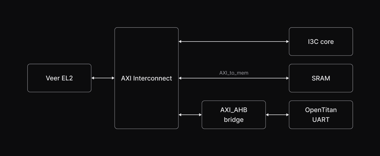
The Guineveer reference System-on-Chip (SoC) design employs the VeeR EL2 core - a 32-bit CPU that supports RISC-V’s extensions for: integer (I), compressed instruction (C), multiplication and division (M), instruction-fetch fence, CSR, and subset of bit manipulation instructions (Z).
The reference design features an AXI system bus which is used to communicate with several peripherals, including an SRAM memory module (accessed via an AXI_to_mem interface), an I3C core, and an AXI-to-AHB bridge (providing access to an OpenTitan UART peripheral).
There are two VeeR cores, each having its own memory and connection to the AXI interconnect.
The SoC is split into two clock domains: one for the I3C core, and one for the rest of the SoC. On FPGA targets, the I3C core is clocked at 160 MHz, while the rest of the SoC is clocked at 32 MHz.
The entire SoC is described in Topwrap/design.yaml, which contains connections, parameters, and modules used in the top module that will be generated by Topwrap.
Currently used peripherals and components
Peripheral |
Source |
|---|---|
VeeR EL2 |
|
AXI Interconnect |
AXI Pulp interconnect wrapper generated by Topwrap |
AXI_AHB bridge |
https://github.com/antmicro/Cores-VeeR-EL2/blob/main/design/lib/axi4_to_ahb.sv |
AXI_to_mem |
https://github.com/pulp-platform/axi/blob/master/src/axi_to_mem.sv |
AXI_cdc |
https://github.com/pulp-platform/axi/blob/master/src/axi_cdc.sv |
UART OpenTitan |
|
I3C core |
Peripheral and component configuration
VeeR EL2
The VeeR EL2 core is configured with FPGA optimizations enabled, and branch predictor, ICCM, DCCM, and I-cache disabled. The full set of configuration options used is found in the root Makefile.
I3C
The I3C core uses mostly its default configuration, with one notable difference: the input sync flip-flops are enabled, which is necessary for FPGAs to prevent glitches.
Memory map
The tables below summarize the Guineveer memory address map in diffrent configurations, including the start, end, and size for the various component types.
Singlecore
Start Address |
End Address |
Size |
Type |
|---|---|---|---|
0x0000_0000 |
0x1FFF_FFFF |
0x1FFF_FFFF |
VeeR EL2 reserved space |
0x3000_1000 |
0x3000_2000 |
0x0000_1000 |
i_axi_cdc_lsu |
0x8000_0000 |
0x8001_F400 |
0x0001_F400 |
lmem0 |
0x3000_0000 |
0x3000_1000 |
0x0000_1000 |
axi_bridge |
Dualcore
Start Address |
End Address |
Size |
Type |
|---|---|---|---|
0x0000_0000 |
0x1FFF_FFFF |
0x1FFF_FFFF |
VeeR EL2 reserved space |
0x3000_1000 |
0x3000_2000 |
0x0000_1000 |
i_axi_cdc_lsu |
0x8000_0000 |
0x8001_F400 |
0x0001_F400 |
lmem0 |
0x9000_0000 |
0x9001_F400 |
0x0001_F400 |
lmem1 |
0x3000_0000 |
0x3000_1000 |
0x0000_1000 |
axi_bridge |