35b0bc5
![]()
Caliptra Hardware Specification
Revision 2.0.3
Scope
This document defines technical specifications for a Caliptra RoT for Measurement (RTM)[1] cryptographic subsystem used in the Open Compute Project (OCP). This document, along with Caliptra: A Datacenter System on a Chip (SoC) Root of Trust (RoT), shall comprise the Caliptra technical specification.
Overview
This document provides definitions and requirements for a Caliptra cryptographic subsystem. The document then relates these definitions to existing technologies, enabling device and platform vendors to better understand those technologies in trusted computing terms.
Caliptra Core
For information on the Caliptra Core, see the High level architecture section of Caliptra: A Datacenter System on a Chip (SoC) Root of Trust (RoT).
Key Caliptra Core 2.0 Changes
- AXI subordinate replaces APB interface of Caliptra 1.x hardware
- SHA Accelerator functionality now available exclusively to Caliptra
- Caliptra uC may use internally in mailbox mode or via the Caliptra AXI DMA assist engine in streaming mode
- SHA Accelerator adds new SHA save/restore functionality
- Adams Bridge Dilithium/ML-DSA (refer to Adams bridge spec)
- Subsystem mode support (refer to Subsystem Specification for details)
- ECDH hardware support
- HMAC512 hardware support
- AXI Manager with DMA support (refer to DMA Specification)
- Manufacturing and Debug Unlock
- UDS programming
- Read logic for Secret Fuses
- Streaming Boot Support
- RISC-V core PMP support
- CSR HMAC key for manufacturing flow
Boot FSM
The Boot FSM detects that the SoC is bringing Caliptra out of reset. Part of this flow involves signaling to the SoC that Caliptra is awake and ready for fuses. After fuses are populated and the SoC indicates that it is done downloading fuses, Caliptra can wake up the rest of the IP by de-asserting the internal reset.
The following figure shows the initial power-on arc of the Mailbox Boot FSM.
Figure 1: Mailbox Boot FSM state diagram
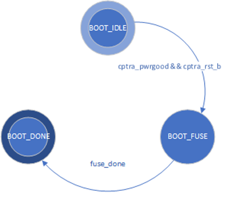
The Boot FSM first waits for the SoC to assert cptra_pwrgood and de-assert cptra_rst_b. In the BOOT_FUSE state, Caliptra signals to the SoC that it is ready for fuses. After the SoC is done writing fuses, it sets the fuse done register and the FSM advances to BOOT_DONE.
BOOT_DONE enables Caliptra reset de-assertion through a two flip-flop synchronizer.
FW update reset (Impactless FW update)
When a firmware update is initiated, Runtime FW writes to fw_update_reset register to trigger the FW update reset. When this register is written, only the RISC-V core is reset using cptra_uc_fw_rst_b pin and all AHB targets are still active. All registers within the targets and ICCM/DCCM memories are intact after the reset. Reset is deasserted synchronously after a programmable number of cycles; the minimum allowed number of wait cycles is 5, which is also the default configured value. Reset de-assertion is done through a two flip-flop synchronizer. Since ICCM is locked during runtime, the boot FSM unlocks it when the RISC-V reset is asserted. Following FW update reset deassertion, normal boot flow updates the ICCM with the new FW from the mailbox SRAM. The boot flow is modified as shown in the following figure.
Figure 2: Mailbox Boot FSM state diagram for FW update reset
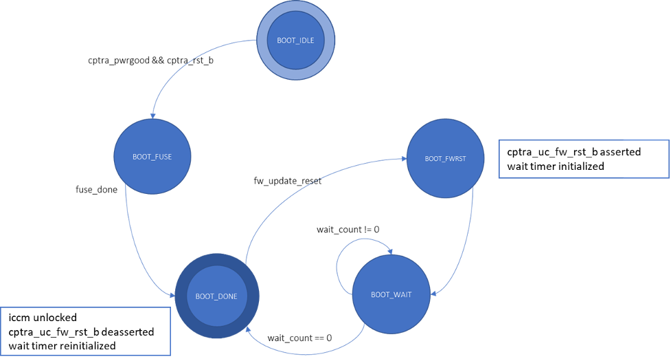
Impactless firmware updates may be initiated by writing to the fw_update_reset register after Caliptra comes out of global reset and enters the BOOT_DONE state. In the BOOT_FWRST state, only the reset to the RISC-V core is asserted and the wait timer is initialized. After the timer expires, the FSM advances from the BOOT_WAIT to BOOT_DONE state where the reset is deasserted and ICCM is unlocked.
RISC-V core
The RISC-V core is VeeR EL2 from CHIPS Alliance. It is a 32-bit CPU core that contains a 4-stage, scalar, in-order pipeline. The core supports RISC-V’s integer(I), compressed instruction(C), multiplication and division (M), instruction-fetch fence, CSR, and subset of bit manipulation instructions (Z) extensions. A link to the RISC-V VeeR EL2 Programmer’s Reference Manual is provided in the References section.
Configuration
The RISC-V core is highly configurable and has the following settings.
| Parameter | Configuration |
|---|---|
| Interface | AHB-Lite |
| DCCM | 256 KiB |
| ICCM | 256 KiB |
| I-Cache | Disabled |
| Reset Vector | 0x00000000 |
| Fast Interrupt Redirect | Enabled |
| External Interrupts | 31 |
| PMP | Enabled |
Embedded memory export
Internal RISC-V SRAM memory components are exported from the Caliptra subsystem to support adaptation to various fabrication processes. For more information, see the Caliptra Integration Specification.
Memory map address regions
The 32-bit address region is subdivided into 16 fixed-sized, contiguous 256 MB regions. The following table describes the address mapping for each of the AHB devices that the RISC-V core interfaces with.
| Subsystem | Address size | Start address | End address |
|---|---|---|---|
| ROM | 96 KiB | 0x0000_0000 | 0x0000_BFFF |
| Cryptographic | 512 KiB | 0x1000_0000 | 0x1007_FFFF |
| Peripherals | 32 KiB | 0x2000_0000 | 0x2000_7FFF |
| SoC IFC | 512 KiB | 0x3000_0000 | 0x3007_FFFF |
| RISC-V Core ICCM | 256 KiB | 0x4000_0000 | 0x4003_FFFF |
| RISC-V Core DCCM | 256 KiB | 0x5000_0000 | 0x5003_FFFF |
| RISC-V MM CSR (PIC) | 256 MiB | 0x6000_0000 | 0x6FFF_FFFF |
Cryptographic subsystem
The following table shows the memory map address ranges for each of the IP blocks in the cryptographic subsystem.
| IP/Peripheral | Target # | Address size | Start address | End address |
|---|---|---|---|---|
| Cryptographic Initialization Engine | 0 | 32 KiB | 0x1000_0000 | 0x1000_7FFF |
| ECC Secp384 | 1 | 32 KiB | 0x1000_8000 | 0x1000_FFFF |
| HMAC512 | 2 | 4 KiB | 0x1001_0000 | 0x1001_0FFF |
| Key Vault | 3 | 8 KiB | 0x1001_8000 | 0x1001_9FFF |
| PCR Vault | 4 | 8 KiB | 0x1001_A000 | 0x1001_BFFF |
| Data Vault | 5 | 8 KiB | 0x1001_C000 | 0x1001_DFFF |
| SHA512 | 6 | 32 KiB | 0x1002_0000 | 0x1002_7FFF |
| SHA256 | 10 | 32 KiB | 0x1002_8000 | 0x1002_FFFF |
| ML-DSA | 14 | 64 KiB | 0x1003_0000 | 0x1003_FFFF |
| AES | 15 | 4 KiB | 0x1001_1000 | 0x1001_1FFF |
Peripherals subsystem
The following table shows the memory map address ranges for each of the IP blocks in the peripherals’ subsystem.
| IP/Peripheral | Target # | Address size | Start address | End address |
|---|---|---|---|---|
| CSRNG | 12 | 4 KiB | 0x2000_2000 | 0x2000_2FFF |
| ENTROPY SRC | 13 | 4 KiB | 0x2000_3000 | 0x2000_3FFF |
SoC interface subsystem
The following table shows the memory map address ranges for each of the IP blocks in the SoC interface subsystem.
| IP/Peripheral | Target # | Address size | Start address | End address |
|---|---|---|---|---|
| Mailbox CSR | 7 | 4 KiB | 0x3002_0000 | 0x3002_0FFF |
| SHA512 Accelerator | 7 | 4 KiB | 0x3002_1000 | 0x3002_1FFF |
| AXI DMA | 7 | 4 KiB | 0x3002_2000 | 0x3002_2FFF |
| SOC IFC CSR | 7 | 64 KiB | 0x3003_0000 | 0x3003_FFFF |
| Mailbox SRAM Direct Access | 7 | 256 KiB | 0x3004_0000 | 0x3007_FFFF |
RISC-V core local memory blocks
The following table shows the memory map address ranges for each of the local memory blocks that interface with RISC-V core.
| IP/Peripheral | Target # | Address size | Start address | End address |
|---|---|---|---|---|
| ICCM0 (via DMA) | 9 | 256 KiB | 0x4000_0000 | 0x4003_FFFF |
| DCCM | 8 | 256 KiB | 0x5000_0000 | 0x5003_FFFF |
Interrupts
The VeeR-EL2 processor supports multiple types of interrupts, including non-maskable interrupts (NMI), software interrupts, timer interrupts, external interrupts, and local interrupts. Local interrupts are events not specified by the RISC-V standard, such as auxiliary timers and correctable errors.
Caliptra uses NMI in conjunction with a watchdog timer to support fatal error recovery and system restart. For more information, see the Watchdog timer section.
Software and local interrupts are not implemented in the first generation of Caliptra. Standard RISC-V timer interrupts are implemented using the mtime and mtimecmp registers defined in the RISC-V Privileged Architecture Specification. Both mtime and mtimecmp are included in the soc_ifc register bank, and are accessible by the internal microprocessor to facilitate precise timing tasks. Frequency for the timers is configured by the SoC using the dedicated timer configuration register, which satisfies the requirement prescribed in the RISC-V specification for such a mechanism. These timer registers drive the timer_int pin into the internal microprocessor.
Non-maskable interrupts
Caliptra's RISC-V processor has access to an internal register that allows configuration of the NMI vector. When an NMI occurs, the program counter jumps to the address indicated by the contents of this register. For more information, see NMI Vector.
External interrupts
Caliptra uses the external interrupt feature to support event notification from all attached peripheral components in the subsystem. The RISC-V processor supports multiple priority levels (ranging from 1-15), which allows firmware to configure interrupt priority per component.
Errors and notifications are allocated as interrupt events for each component, with error interrupts assigned a higher priority and expected to be infrequent.
Notification interrupts are used to alert the processor of normal operation activity, such as completion of requested operations or arrival of SoC requests through the shared interface.
Vector 0 is reserved by the RISC-V processor and may not be used, so vector assignment begins with Vector 1. Bit 0 of the interrupt port to the processor corresponds with Vector 1. The following table shows assignment of interrupt vectors to the corresponding IP block. The illustrated interrupt priority assignment is only an example, and does not correspond with actual priorities assigned in the final Caliptra firmware. These interrupt priorities are used in the validation firmware that tests the RTL, and are defined in caliptra_defines.h.
| IP/Peripheral | Interrupt vector | Interrupt priority example (Increasing, Max 15) |
|---|---|---|
| Cryptographic Initialization Engine (Errors) | 1 | 8 |
| Cryptographic Initialization Engine (Notifications) | 2 | 7 |
| ECC (Errors) | 3 | 8 |
| ECC (Notifications) | 4 | 7 |
| HMAC (Errors) | 5 | 8 |
| HMAC (Notifications) | 6 | 7 |
| Key Vault (Errors) | 7 | 8 |
| Key Vault (Notifications) | 8 | 7 |
| SHA512 (Errors) | 9 | 8 |
| SHA512 (Notifications) | 10 | 7 |
| SHA256 (Errors) | 11 | 8 |
| SHA256 (Notifications) | 12 | 7 |
| RESERVED | 13, 15, 17 | 4 |
| RESERVED | 14, 16, 18 | 3 |
| Mailbox (Errors) | 19 | 8 |
| Mailbox (Notifications) | 20 | 7 |
| SHA512 Accelerator (Errors) | 23 | 8 |
| SHA512 Accelerator (Notifications) | 24 | 7 |
| MLDSA (Errors) | 23 | 8 |
| MLDSA (Notifications) | 24 | 7 |
| AXI DMA (Errors) | 25 | 8 |
| AXI DMA (Notifications) | 26 | 7 |
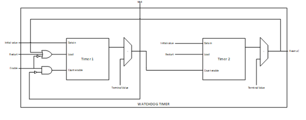
Watchdog timer
The primary function of Caliptra Watchdog Timer (WDT) is to reset the microcontroller (Caliptra), in the event of a software malfunction, by resetting the device if it has not been cleared in software. It is a two-stage timer, independent of the RISCV core.
Operation
The WDT consists of two timers. When enabled in cascade mode (done by enabling Timer 1 alone), the WDT increments Timer 1 until the counter rolls over or times out. Typically, the timer is serviced at regular intervals to prevent it from overflowing or rolling over. If Timer 1 has not timed out, Timer 2 is disabled and held at its initial value. However, when Timer 1 does roll over, it triggers an error interrupt to the RISC-V core. In parallel, Timer 2 is enabled and begins counting. If the interrupt is serviced before Timer 2 times out, the timers are reset and continue to operate normally. If Timer 2 times out, it asserts an SoC fatal error and an NMI. The SoC fatal error is also captured in the CPTRA_HW_ERROR_FATAL register, which can be cleared by the SoC by writing a 1. A warm reset is required by the SoC to reset the timers when Timer 2 times out.
The WDT timers can be configured to operate independent of each other. When the enable register for Timer 2 is set, the default configuration of cascaded timers is disabled and both timers count independently of each other. In this case, a timeout on Timer 2 causes an error interrupt to the RISC-V core similar to Timer 1. Disabling Timer 2 configures the timers back into the default cascaded mode.
Each timer has an enable bit, a restart bit, and a 64-bit timeout value register that can be programmed as needed. The restart bit is used to service the timers and restart counting. The timeout period registers can be configured to the desired upper bound of timers.
If the WDT timers are disabled and then re-enabled with a new timeout period, they must be restarted by setting the appropriate control register (restart bit). If the timers are temporarily disabled and re-enabled with the same timeout period, they resume counting and do not restart from 0.
For more details regarding the register interface to control the WDT, see the register documentation published in the RTL GitHub repository.
The following figure shows the two timers.
Figure 3: Caliptra Watchdog Timer
Prescale settings
Assuming a clock source of 500 MHz, a timeout value of 32’hFFFF_FFFF results in a timeout period of ~8.5 seconds. Two 32-bit registers are provided for each timer, allowing a 64-bit timeout period to be programmed for each timer. This accommodates a maximum timeout value of over 1000 years for the same 500 Mhz clock source.
Microcontroller interface
The Caliptra microcontroller communicates with the mailbox through its internal AHB-Lite fabric.
AHB-lite interface
AHB-lite is a subset of the full AHB specification. It is primarily used in single initiator systems. This interface connects VeeR EL2 Core (LSU initiator) to the target devices. See Caliptra Core for information.
The interface can be customized to support variable address and data widths, and a variable number of target devices. Each target device is assigned an address range within the 32-bit address memory map region. The interface includes address decoding logic to route data to the appropriate AHB target device based on the address specified.
The integration parameters for Caliptra’s AHB-lite interface are shown in the following table.
| Parameter | Value |
|---|---|
| ADDRESS_WIDTH | 32 |
| DATA_WIDTH | 64 |
| NUM_OF_SLAVES | 17 |
Each IP component in the Caliptra system uses a native AHB data width of 32-bits (1 dword). The AHB responder logic in each IP component contains width conversion logic that transforms from the fabric data width of 64-bits to this native 32-bit width. The conversion involves calculating the dword offset (either 0 or 1) relative to the native 64-bit width by evaluating bit [2] of the address line. This information is used to extract the correct 32-bits from the native write data line. If there is a data offset, data is shifted down by 32-bits; otherwise, the upper 32-bits are simply truncated. This new dword-address is passed to the internal register interface along with the dword-sized data. A similar conversion works in reverse to correctly place read data in the response data line from the responder.
As a result of this implementation, 64-bit data transfers are not supported on the Caliptra AHB fabric. Firmware running on the internal microprocessor may only access memory and registers using a 32-bit or smaller request size, as 64-bit transfer requests will be corrupted.
All AHB requests internal to Caliptra must be to an address that is aligned to the native data width of 4-bytes. Any AHB read or write by the Caliptra RISC-V processor that is not aligned to this boundary will fail to decode to the targeted register, will fail to write the submitted data, and will return read data of all zeroes. All AHB requests must also use the native size of 4 bytes (encoded in the hsize signal with a value of 2). The only exception to this is when the RISC-V processor performs byte-aligned, single-byte reads to the Mailbox SRAM using the direct-access mechanism described in SoC Mailbox. In this case, a byte-aligned address must be accompanied by the correct size indicator for a single-byte access. Read addresses for byte accesses are aligned to the 4-byte boundary in hardware, and will successfully complete with the correct data at the specified byte offset. Direct mode SRAM writes must be 4-bytes in size and must be aligned to the 4-byte boundary. Hardware writes the entire dword of data to the aligned address, so attempts to write a partial word of data may result in data corruption.
Cryptographic subsystem
For details, see the Cryptographic subsystem architecture section.
SoC mailbox
For more information on the mailbox protocol, see Mailbox in the Caliptra Integration Specification. Mailbox registers accessible to the Caliptra microcontroller are defined in internal-regs/mbox_csr.
The RISC-V processor is able to access the SoC mailbox SRAM using a direct access mode (which bypasses the defined mailbox protocol). The addresses for performing this access are described in SoC interface subsystem and in mbox_sram. In this mode, firmware must first acquire the mailbox lock. Then, reads and writes to the direct access address region will go directly to the SRAM block. Firmware must release the mailbox lock by writing to the mbox_unlock register after direct access operations are completed.
Security state
Caliptra uses the MSB of the security state input to determine whether or not Caliptra is in debug mode.
When Caliptra is in debug mode:
-
Security state MSB is set to 0.
-
Caliptra JTAG is opened for the microcontroller and HW debug.
-
Device secrets (UDS, FE, key vault, csr hmac key and obfuscation key) are programmed to debug values.
If a transition to debug mode happens during ROM operation, any values computed from the use of device secrets may not match expected values.
Transitions to debug mode trigger a hardware clear of all device secrets, and also trigger an interrupt to FW to inform of the transition. FW is responsible for initiating another hardware clear of device secrets utilizing the clear secrets register, in case any derivations were in progress and stored after the transition was detected. FW may open the JTAG after all secrets are cleared.
Debug mode values may be set by integrators in the Caliptra configuration files. The default values are shown in the following table.
| Name | Default value |
|---|---|
| Obfuscation Key Debug Value | All 0x1 |
| CSR HMAC Key Debug Value | All 0x1 |
| UDS Debug Value | All 0x1 |
| Field Entropy Debug Value | All 0x1 |
| Key Vault Debug Value 0 | All 0xA |
| Key Vault Debug Value 1 | All 0x5 |
Note: When entering debug or scan mode, all crypto engines are zeroized. Before starting any crypto operation in these modes, the status registers of all crypto engines must be checked to confirm they are ready. Failing to do so may trigger a fatal error caused by concurrent crypto operations.
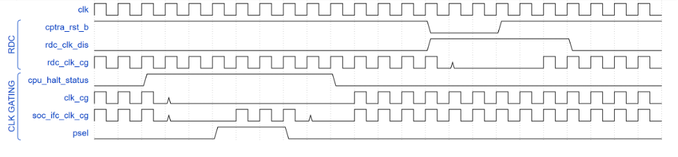
Clock gating
Caliptra provides a clock gating feature that turns off clocks when the microcontroller is halted. Clock gating is disabled by default, but can be globally enabled via the following register.
| Control register | Start address | Description |
|---|---|---|
| CPTRA_CLK_GATING_EN | 0x300300bc | Register bit to enable or disable the clock gating feature. |
When enabled, halting the microcontroller turns off clocks to all of the cryptographic subsystem, the vaults (key vault, PCR vault, and data vault), mailbox SRAM, SoC interface, and peripherals subsystem. The Watchdog timer and SoC registers run on the gated RDC clock. The RV core implements its own clock gating mechanism. Halting the core automatically turns off its clock.
There are a total of 4 clocks in Caliptra: ungated clock, gated clock, gated RDC clock, and gated SoC IFC clock. The following table shows the different modules and their designated clocks.
| Module | Clock |
|---|---|
| RV core | Clk |
| SOC IFC | Clk; clk_cg; rdc_clk_cg; soc_ifc_clk_cg |
| Crypto subsystem | Clk_cg |
| Vaults | Clk_cg |
| Peripherals subsystem | Clk_cg |
| AHB Lite IF, 2to1 Mux | Clk_cg |
| TRNG | Clk_cg |
Wake up conditions
For details on halting the core and waking up the core from the halt state, see section 5 of the RISC-V VeeR EL2 Programmer's Reference Manual.
When the RV core wakes up, all clocks are enabled. However, when the core is halted, it is possible to wake up Caliptra clocks through:
-
A change in generic_input_wires
-
Cptra_fatal_error assertion
-
Entry to debug or scan modes
-
JTAG accesses
-
AXI transactions
Activity on the AXI subordinate interface only wakes up the SoC IFC clock. All other clocks remain off until any other condition is met or the core exits the halt state.
| Cpu_halt_status | s_axi_active | Generic input wires || fatal error || debug/scan mode ||JTAG access | Expected behavior |
|---|---|---|---|
| 0 | X | X | All gated clocks active |
| 1 | 0 | 0 | All gated clocks inactive |
| 1 | 0 | 1 | All gated clocks active (as long as condition is true) |
| 1 | 1 | 0 | Soc_ifc_clk_cg active (as long as s_axi_active = 1) All other clks inactive |
| 1 | 1 | 1 | Soc_ifc_clk_cg active (as long as condition is true OR s_axi_active = 1) All other clks active (as long as condition is true) |
Usage
The following applies to the clock gating feature:
- The core should only be halted after all pending vault writes are done and cryptographic operations are complete.
- While the core is halted, any AXI transaction wakes up the SoC interface clock and leaves all other clocks disabled. If the core is still halted when the AXI transactions are done, the SoC interface clock is returned to a disabled state. .
- The RDC clock is similar to an ungated clock and is only disabled when a reset event occurs. This avoids metastability on flops. The RDC clock operates independently of core halt status.
Timing information
The following figure shows the timing information for clock gating.
Figure 10: Clock gating timing
Integrated TRNG
Caliptra implements a true random number generator (TRNG) block for local use models. Firmware is able to read a random number from the TRNG core by accessing its register block over the AHB-lite interface. This is a configuration that SoC integrators enable by defining CALIPTRA_INTERNAL_TRNG.
This TRNG block is a combination of entropy source and CSRNG implementations. For information, see the ENTROPY_SRC HWIP Technical Specification and the CSRNG HWIP Technical Specification. The core code (see entropy source and csrng) is reused from here but the interface to the module is changed to AHB-lite. This design provides an interface to an external physical random noise generator. This is also referred to as a physical true random number generator (PTRNG). The PTRNG external source is a physical true random noise source. A noise source and its relation to an entropy source are defined by SP 800-90B.
The block is instantiated based on a design parameter chosen at integration time. This is to provide options for SoC to reuse an existing TRNG to build an optimized SoC design. For the optimized scenarios, SoC needs to follow the External-TRNG REQ HW API.
The following figure shows the integrated TRNG block.
Figure 11: Integrated TRNG block
The following figure shows the CSRNG block.
Figure 12: CSRNG block
The following figure shows the entropy source block.
Figure 13: Entropy source block
Operation
Requests for entropy bits start with command requests over the AHB-lite interface to the csrng CMD_REQ register.
The following describes the fields of the command request header:
-
Application Command: Selects one of five operations to perform. The commands supported are instantiate, reseed, generate, update, and uninstantiate.
-
Command Length: Number of 32-bit words that can optionally be appended to the command. A value of zero will only transfer the command header. A value of 4'hc transfers the header plus an additional twelve 32-bit words of data.
-
Command Flag0: flag0 is associated with the current command. Setting this field to True (4’h6) enables flag0 to be enabled. Note that flag0 is used for the instantiate and reseed commands only; for all other commands, the flag0 value is ignored.
-
Generate Length: Only defined for the generate command, this field is the total number of cryptographic entropy blocks requested. Each unit represents 128 bits of entropy returned. A value of 8 would return a total of 1024 bits. The maximum size supported is 4096.
First an instantiate command is requested over the SW application interface to initialize an instance in the CSRNG module. Depending on the flag0 and clen fields in the command header, a request to the entropy_src module over the entropy interface is sent to seed the csrng. This can take a few milliseconds if the seed entropy is not immediately available.
Example instantiation:
acmd = 0x1 (Instantiate)
clen/flag0 = The seed behavior is described in the following table.
glen = Not used
| flag0 | clen | Description |
|---|---|---|
| F | 0 | Only entropy source seed is used. |
| F | 1-12 | Entropy source seed is xor'ed with provided additional data. |
| T | 0 | Seed of zero is used (no entropy source seed used). |
| T | 1-12 | Only provided additional data is used as seed. |
Next a generate command is used to request generation of cryptographic entropy bits. The glen field defines how many 128 bit words are to be returned to the application interface. After the generated bits are ready, they can be read out via the GENBITS register. This register must be read out glen * 4 times for each request made.
Example generate command:
acmd = 0x3 (Generate)
clen = 0
flag0 = false (4’h9)
glen = 4 (4 *128 = 512b)
This requires 16 reads from GENBITS to read out all of the generated entropy.
Configuration
The HW application interfaces are not supported. Only the SW application interface should be used for this design.
Physical true random noise source signal descriptions
These are the top level signals defined in caliptra_top.
| Name | Input or output | Description |
|---|---|---|
| itrng_data | input | Physical true random noise source data |
| itrng_valid | input | Valid is asserted high for one cycle when data is valid. The expected valid output rate is about 50KHz. |
The following figure shows the top level signals defined in caliptra_top.
Figure 14: caliptra_top signals
Entropy source signal descriptions
The following table provides descriptions of the entropy source signals.
| Name | Input or output | Description |
|---|---|---|
| clk_i | input | All signal timings are related to the rising edge of clk. |
| rst_ni | input | The reset signal is active LOW and resets the core. |
| entropy_src_rng_req | output | Request from the entropy_src module to the physical true random noise source to start generating data. |
| entropy_src_rng_rsp | input | Contains the internal TRNG data and a flag indicating the data is valid. Valid is asserted high for one cycle when data is valid. |
| entropy_src_hw_if_i | input | Downstream block request for entropy bits. |
| entropy_src_hw_if_o | output | 384 bits of entropy data. Valid when es_ack is asserted high. |
| cs_aes_halt_i | input | Response from csrng that all requests to AES block are halted. |
| cs_aes_halt_o | output | Request to csrng to halt requests to the AES block for power leveling purposes. |
The following figure shows the entropy source signals.
Figure 15: Entropy source signals
CSRNG signal descriptions
The following table provides descriptions for the CSRNG signals.
| Name | Input or output | Description |
|---|---|---|
| clk_i | input | All signal timings are related to the rising edge of clk. |
| rst_ni | input | The reset signal is active LOW and resets the core. |
| otp_en_csrng_sw_app_read_i | input | Enable firmware to access the ctr_drbg internal state and genbits through registers. |
| lc_hw_debug_en_i | input | Lifecycle that selects which diversification value is used for xoring with the seed from entropy_src. |
| entropy_src_hw_if_i | input | 384 bits of entropy data. Valid when es_ack is asserted high. |
| entropy_src_hw_if_o | output | Downstream block request for entropy bits. |
| cs_aes_halt_i | input | Request from entropy_src to halt requests to the AES block for power leveling purposes. |
| cs_aes_halt_o | output | Response to entropy_src that all requests to AES block are halted. |
The CSRNG may only be enabled if entropy_src is enabled. After it is disabled, CSRNG may only be re-enabled after entropy_src has been disabled and re-enabled.
FIPS considerations
The following sections illustrate the self-test parameter configuration. The
entropy_src block provides additional tests, but Caliptra focuses primarily
on the adaptive and repetition count tests, which are the ones strictly
required for FIPS compliance. Additional details can be found in NIST
publication SP 800-90B.
The TRNG must be re-initialized whenever self-test parameter changes are needed. As described in the previous section, the initialization steps are as follows:
- Disable
csrngandentropy_srcin that order. - Apply new self-test configuration.
- Enable
entropy_srcandcsrngin that order.
Adaptive self-test window and thresholds
This section details the configuration of the entropy_src, focusing on how
the test window size for the adaptive self-test is determined and how it
relates to threshold calculations.
Understanding Test Window Sizes
The adaptive self-test within the entropy_src block utilizes a
configurable test window. To clarify its interpretation, two terms are
defined:
ENTROPY_TEST_WINDOW: This refers to the test window size directly configured in the hardware registers of theentropy_srcblock.ACTUAL_TEST_WINDOW: This refers to the effective window size used for the adaptive self-test threshold calculations. Its value depends on how the test scores are aggregated.
The aggregation method is determined by the CONF.THRESHOLD_SCOPE setting in the entropy_src block.
Aggregate per symbol
When CONF.THRESHOLD_SCOPE is enabled:
- The adaptive test combines the inputs from all physical entropy lines into a single, cumulative score.
- The test essentially treats the combined input as a single binary stream, counting the occurrences of '1's.
- In this configuration:
- If
ENTROPY_TEST_WINDOWis set to 1024, then ACTUAL_TEST_WINDOW=ENTROPY_TEST_WINDOW= 1024
- If
Handle each physical noise source separately
When CONF.THRESHOLD_SCOPE is disabled:
- The adaptive test scores each individual physical noise input line independently.
- This allows for monitoring the health of each noise source.
- In this configuration (assuming, for example, 4 noise sources):
- If
ENTROPY_TEST_WINDOWis set to 4096 bits, then ACTUAL_TEST_WINDOW= (ENTROPY_TEST_WINDOW/ 4) = 1024
- If
Configuring adaptive self-test thresholds
Once the ACTUAL_TEST_WINDOW is determined, the adaptive self-test
thresholds can be configured as follows:
ADAPTP_HI_THRESHOLDS.FIPS_THRESH=adaptp_cutoffADAPTP_LO_THRESHOLDS.FIPS_THRESH=ACTUAL_TEST_WINDOW-adaptp_cutoff
Here, adaptp_cutoff represents the pre-determined cutoff value for the
adaptive proportion test, as defined by NIST SP 800-90B. See the threshold
calculations below as an example.
\(α = 2^{-40}\) (recommended)
\(H = 0.5\) (example, estimated entropy measured from hardware)
\(W\) = ACTUAL_TEST_WINDOW
adaptp_cutoff = \(1 + critbinom(W, 2^{-H}, 1 - α)\)
Note: The
critbinomfunction (critical binomial distribution function) is implemented by most spreadsheet applications.
Recommended configuration
The following configuration is recommended for the adaptive and repetition count tests:
Adaptive test
- Set
CONF.THRESHOLD_SCOPEto disabled. This allows the test to monitor and score each physical noise source individually, providing more granular health information. - Set
HEALTH_TEST_WINDOWS.FIPS_WINDOWto 4096 bits. This value serves as theENTROPY_TEST_WINDOW. With the current 4 noise source configuration, this is equivalent to 1024 bits per noise source, where each source produces 1 bit of entropy as defined in NIST SP 800-90B. - Calculate thresholds. Use an
ACTUAL_TEST_WINDOWof 1024 bits (derived from step 2) in the adaptive test threshold formulas provided earlier in this subsection.
Repetition count test
The methodology used for calculating the repetition count threshold in the ROM boot phase can be directly applied for this test as well. The threshold is applied on a per-noise-source basis.
External-TRNG REQ HW API
For SoCs that choose to not instantiate Caliptra’s integrated TRNG, Caliptra provides a TRNGREQ HW API.
- Caliptra asserts TRNG_REQ wire (FW made the request for a TRNG).
- SoC writes the TRNG architectural registers.
- SoC writes a done bit in the TRNG architectural registers.
- Caliptra desserts TRNG_REQ.
The reason to have a separate interface from the SoC mailbox is to ensure that this request is not intercepted by any SoC FW agents that communicate with the SoC mailbox. It is required for FIPS compliance that this TRNG HW API is always handled by a SoC HW gasket logic and not handled by SoC ROM/FW code.
SoC-SHA accelerator HW API
Caliptra provides a SHA accelerator HW API for Caliptra internal FW to use via mailbox or via DMA operations through the AXI subordinate interface. The SHA accelerator HW API is restricted on AXI for use by Caliptra via the AXI DMA assist block; this access restriction is enforced by checking logic on the AXI AxUSER signal associated with the request.
Using the HW API:
- A user of the HW API first locks the accelerator by reading the LOCK register. A read that returns the value 0 indicates that the resource was locked for exclusive use by the requesting user. A write of ‘1 clears the lock.
- The USER register captures the AXI USERID value of the requestor that locked the SHA accelerator. This is the only user that is allowed to control the SHA accelerator by performing AXI register writes. Writes by any other agent on the AXI subordinate interface are dropped.
- SHA supports Mailbox mode: SHA is computed on LENGTH (DLEN) bytes of data stored in the mailbox beginning at START_ADDRESS. This computation is performed when the EXECUTE register is set by the user. When the operation is completed and the result in the DIGEST register is valid, SHA accelerator sets the VALID bit of the STATUS register.
- Note that even though the mailbox size is fixed, due to SHA save/restore function enhancement, there is no limit on the size of the block that needs to be SHAd. SOC needs to follow FW API
- The SHA computation engine in the SHA accelerator requires big endian data, but the SHA accelerator can accommodate mailbox input data in either the little endian or big endian format. By default, input data is assumed to be little endian and is swizzled to big endian at the byte level prior to computation. For the big endian format, data is loaded into the SHA engine as-is. Users may configure the SHA accelerator to treat data as big endian by setting the ENDIAN_TOGGLE bit appropriately.
- See the register definition for the encodings.
- SHA engine also provides a ‘zeroize’ function through its CONTROL register to clear any of the SHA internal state. This can be used when the user wants to conceal previous state for debug or security reasons.
JTAG implementation
For specific debug flows, see the JTAG/TAP Debug section in Caliptra: A Datacenter System on a Chip (SoC) Root of Trust (RoT).
The following figure shows the JTAG implementation within the Caliptra boundary. The output of the existing DMI wrapper is used to find the non-Core (Caliptra uncore) aperture to route the JTAG commands.
Caliptra’s JTAG/TAP should be implemented as a TAP EP. JTAG is open if the debug mode is set at the time of Caliptra reset deassertion.
Note: If the debug security state switches to debug mode anytime, the security assets and keys are still flushed even though JTAG is not open.
Figure 16: JTAG implementation
Cryptographic subsystem architecture
The architecture of Caliptra cryptographic subsystem includes the following components:
- Symmetric cryptographic primitives
- De-obfuscation engine
- SHA512/384 (based on NIST FIPS 180-4 [2])
- SHA256 (based on NIST FIPS 180-4 [2])
- HMAC512 (based on NIST FIPS 198-1 [5] and RFC 4868 [6])
- Public-key cryptography
- NIST Secp384r1 Deterministic Digital Signature Algorithm (based on FIPS-186-4 [11] and RFC 6979 [7])
- Key vault
- Key slots
- Key slot management
The high-level architecture of Caliptra cryptographic subsystem is shown in the following figure.
Figure 17: Caliptra cryptographic subsystem
SHA512/SHA384
SHA512 is a function of cryptographic hash algorithm SHA-2. The hardware implementation is based on Secworks/SHA512 [1]. This implementation complies with the functionality in NIST FIPS 180-4 [2]. The implementation supports the SHA512 variants SHA-512/224, SHA-512/256, SHA384 and SHA512.
The SHA512 algorithm is described as follows:
- The message is padded by the host and broken into 1024-bit chunks
- For each chunk:
- The message is fed to the SHA512 core
- The core should be triggered by the host
- The SHA512 core status is changed to ready after hash processing
- The result digest can be read after feeding all message chunks
Operation
Padding
The message should be padded before feeding to the hash core. The input message is taken, and some padding bits are appended to it to get it to the desired length. The bits that are used for padding are simply ‘0’ bits with a leading ‘1’ (100000…000). The appended length of the message (before pre-processing), in bits, is a 128-bit big-endian integer.
The total size should be equal to 128 bits short of a multiple of 1024 since the goal is to have the formatted message size as a multiple of 1024 bits (N x 1024). The following figure shows the SHA512 input formatting.
Figure 18: SHA512 input formatting
Hashing
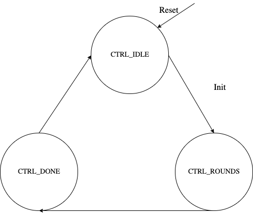
The SHA512 core performs 80 iterative operations to process the hash value of the given message. The algorithm processes each block of 1024 bits from the message using the result from the previous block. For the first block, the initial vectors (IV) are used for starting the chain processing of each 1024-bit block.
FSM
The SHA512 architecture has the finite-state machine as shown in the following figure.
Figure 19: SHA512 FSM
Signal descriptions
The SHA512 architecture inputs and outputs are described in the following table.
| Name | Inputs and outputs | Description |
|---|---|---|
| clk | input | All signal timings are related to the rising edge of clk. |
| reset_n | input | The reset signal is active LOW and resets the core. This is the only active LOW signal. |
| init | input | The core is initialized and processes the first block of message. |
| next | input | The core processes the rest of the message blocks using the result from the previous blocks. |
| mode[1:0] | input | Indicates the hash type of the function. This can be: - SHA512/224 - SHA512/256 - SHA384 - SHA512 |
| zeroize | input | The core clears all internal registers to avoid any SCA information leakage. |
| block[1023:0] | input | The input padded block of message. |
| ready | output | When HIGH, the signal indicates the core is ready. |
| digest[511:0] | output | The hashed value of the given block. |
| digest_valid | output | When HIGH, the signal indicates that the result is ready. |
Address map
The SHA512 address map is shown here: sha512_reg — clp Reference (chipsalliance.github.io)
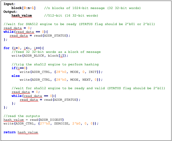
Pseudocode
The following pseudocode demonstrates how the SHA512 interface can be implemented.
Figure 20: SHA512 pseudocode
SCA countermeasure
We do not propose any countermeasure to protect the hash functions. Inherently, hash functions do not work like other cryptographic engines. Hash functions target integrity without requiring a secret key. Hence, the attacker can target only messages. Also, the attacker cannot build a CPA or DPA platform on the hash function because the same message ideally gives the same side-channel behavior.
If the attacker works on the multi-message mechanism, the attacker then needs to work with single trace attacks, which are very unlikely in ASIC/FPGA implementations. Also, our hash implementation is a noisy platform. As a result, we do not propose any SCA implementation countermeasure on the hash functions.
Performance
The SHA512 core performance is reported considering two different architectures: pure hardware architecture, and hardware/software architecture. These are described next.
Pure hardware architecture
In this architecture, the SHA512 interface and controller are implemented in hardware. The performance specification of the SHA512 architecture is shown in the following table.
| Operation | Cycle count [CCs] | Time [us] @ 400 MHz | Throughput [op/s] |
|---|---|---|---|
| Data_In transmission | 0.08 | ||
| Process | 87 | 0.22 | |
| Data_Out transmission | 16 | 0.04 | |
| Single block | 136 | 0.34 | 2,941,176 |
| Double block | 224 | 0.56 | 1,785,714 |
| 1 KiB message | 840 | 2.10 | 476,190 |
| 128 KiB message | 17,632 | 44.08 | 22,686 |
Hardware/software architecture
In this architecture, the SHA512 interface and controller are implemented in RISC-V core. The performance specification of the SHA512 architecture is shown in the following table.
| Operation | Cycle count [CCs] | Time [us]] @ 400 MHz | Throughput [op/s] |
|---|---|---|---|
| Data_In transmission | 990 | 2.48 | |
| Process | 139 | 0.35 | |
| Data_Out transmission | 387 | 0.97 | |
| Single block | 1,516 | 3.79 | 263,852 |
| Double block | 2,506 | 6.27 | 159,617 |
| 1 KiB message | 9,436 | 23.59 | 42,391 |
| 128 KiB message | 1,015,276 | 2,538.19 | 394 |
Pure software architecture
In this architecture, the SHA512 algorithm is implemented fully in software. The implementation is derived from the OpenSSL SHA512 implementation [3]. The performance numbers for this architecture are shown in the following table.
| Data size | Cycle count |
|---|---|
| 1 KiB | 147,002 |
| 4 KiB | 532,615 |
| 8 KiB | 1,046,727 |
| 12 KiB | 1,560,839 |
| 128 KiB | 16,470,055 |
SHA256
SHA256 is a function of the SHA-2 cryptographic hash algorithm. The hardware implementation is based on Secworks/SHA256 [1]. The implementation supports the two variants: SHA256/224 and SHA256.
The SHA256 algorithm is described as follows:
- The message is padded by the host and broken into 512-bit chunks
- For each chunk:
- The message is fed to the sha256 core
- The core should be triggered by the host
- The sha256 core status is changed to ready after hash processing
- The result digest can be read after feeding all message chunks
Operation
Padding
The message should be padded before feeding to the hash core. The input message is taken, and some padding bits are appended to the message to get it to the desired length. The bits that are used for padding are simply ‘0’ bits with a leading ‘1’ (100000…000). The appended length of the message (before pre-processing), in bits, is a 64-bit big-endian integer.
The total size should be equal to 64 bits, short of a multiple of 512 because the goal is to have the formatted message size as a multiple of 512 bits (N x 512).
The following figure shows SHA256 input formatting.
Figure 21: SHA256 input formatting

Hashing
The SHA256 core performs 64 iterative operations to process the hash value of the given message. The algorithm processes each block of 512 bits from the message using the result from the previous block. For the first block, the initial vectors (IV) are used to start the chain processing of each 512-bit block.
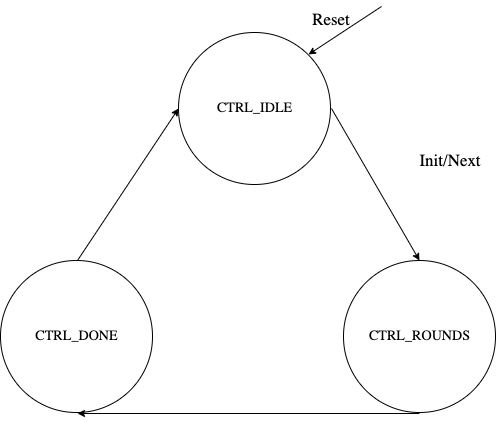
FSM
The SHA256 architecture has the finite-state machine as shown in the following figure.
Figure 22: SHA256 FSM
Signal descriptions
The SHA256 architecture inputs and outputs are described as follows.
| Name | Input or output | Description |
|---|---|---|
| clk | input | All signal timings are related to the rising edge of clk. |
| reset_n | input | The reset signal is active LOW and resets the core. This is the only active LOW signal. |
| init | input | The core is initialized and processes the first block of message. |
| next | input | The core processes the rest of the message blocks using the result from the previous blocks. |
| mode | input | Indicates the hash type of the function. This can be: - SHA256/224 - SHA256 |
| zeroize | input | The core clears all internal registers to avoid any SCA information leakage. |
| WNTZ_MODE* | input | SHA256 core is configured in Winternitz verification mode. |
| WNTZ_W[3:0]* | input | Winternitz W value. |
| WNTZ_N_MODE* | input | Winternitz n value(SHA192/SHA256 --> n = 24/32) |
| block[511:0] | input | The input padded block of message. |
| ready | output | When HIGH, the signal indicates the core is ready. |
| digest[255:0] | output | The hashed value of the given block. |
| digest_valid | output | When HIGH, the signal indicates the result is ready. |
* For more imformation about these inputs, please refer to LMS accelerator section.
Address map
The SHA256 address map is shown here: sha256_reg — clp Reference (chipsalliance.github.io).
Pseudocode
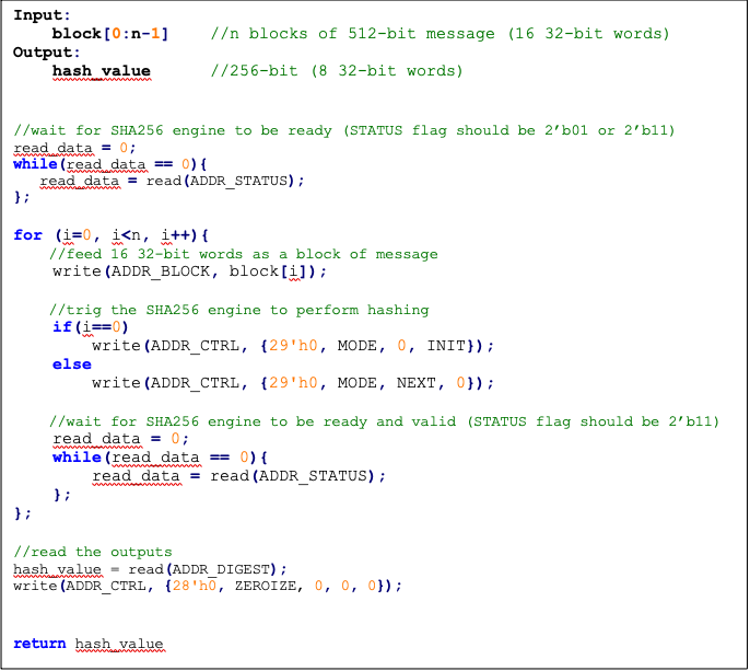
The following pseudocode demonstrates how the SHA256 interface can be implemented.
Figure 23: SHA256 pseudocode
SCA countermeasure
We do not propose any countermeasure to protect the hash functions. For more information, see SCA countermeasure in the SHA512/SHA384 section.
Performance
The SHA256 core performance is reported considering two different architectures: pure hardware architecture, and hardware/software architecture. These are described next.
Pure hardware architecture
In this architecture, the SHA256 interface and controller are implemented in hardware. The performance specification of the SHA256 architecture is reported as shown in the following table.
| Operation | Cycle count [CCs] | Time [us] @ 400 MHz | Throughput [op/s] |
|---|---|---|---|
| Data_In transmission | 17 | 0.04 | |
| Process | 66 | 0.17 | |
| Data_Out transmission | 8 | 0.02 | |
| Single block | 91 | 0.23 | 4,395,604 |
| Double block | 158 | 0.40 | 2,531,646 |
| 1 KiB message | 1163 | 2.91 | 343,938 |
Hardware/software architecture
In this architecture, the SHA256 interface and controller are implemented in RISC-V core. The performance specification of the SHA256 architecture is reported as shown in the following table.
| Operation | Cycle count [CCs] | Time [us] @ 400 MHz | Throughput [op/s] |
|---|---|---|---|
| Data_In transmission | 500 | 1.25 | |
| Process | 66 | 0.17 | |
| Data_Out transmission | 195 | 0.49 | |
| Single block | 761 | 1.90 | 525,624 |
| Double block | 1355 | 3.39 | 295,203 |
| 1 KiB message | 8761 | 21.90 | 45,657 |
HMAC512/HMAC384
Hash-based message authentication code (HMAC) is a cryptographic authentication technique that uses a hash function and a secret key. HMAC involves a cryptographic hash function and a secret cryptographic key. This implementation supports the HMAC512 variants HMAC-SHA-512-256 and HMAC-SHA-384-192 as specified in NIST FIPS 198-1 [5]. The implementation is compatible with the HMAC-SHA-512-256 and HMAC-SHA-384-192 authentication and integrity functions defined in RFC 4868 [6].
Caliptra HMAC implementation uses SHA512 as the hash function, accepts a 512-bit key, and generates a 512-bit tag.
The implementation also supports PRF-HMAC-SHA-512. The PRF-HMAC-SHA-512 algorithm is identical to HMAC-SHA-512-256, except that variable-length keys are permitted, and the truncation step is not performed.
The HMAC algorithm is described as follows:
- The key is fed to the HMAC core to be padded
- The message is broken into 1024-bit chunks by the host
- For each chunk:
- The message is fed to the HMAC core
- The HMAC core should be triggered by the host
- The HMAC core status is changed to ready after hash processing
- The result digest can be read after feeding all message chunks
Operation
Padding
The message should be padded before feeding to the HMAC core. Internally, the i_padded key is concatenated with the message. The input message is taken, and some padding bits are appended to the message to get it to the desired length. The bits that are used for padding are simply ‘0’ bits with a leading ‘1’ (100000…000).
The total size should be equal to 128 bits, short of a multiple of 1024 because the goal is to have the formatted message size as a multiple of 1024 bits (N x 1024).
Figure 24: HMAC input formatting
The following figures show examples of input formatting for different message lengths.
Figure 25: Message length of 1023 bits
When the message is 1023 bits long, padding is given in the next block along with message size.
Figure 26: 1 bit padding
When the message size is 895 bits, a padding of ‘1’ is also considered valid, followed by the message size.
Figure 27: Multi block message
Messages with a length greater than 1024 bits are broken down into N 1024-bit blocks. The last block contains padding and the size of the message.
Hashing
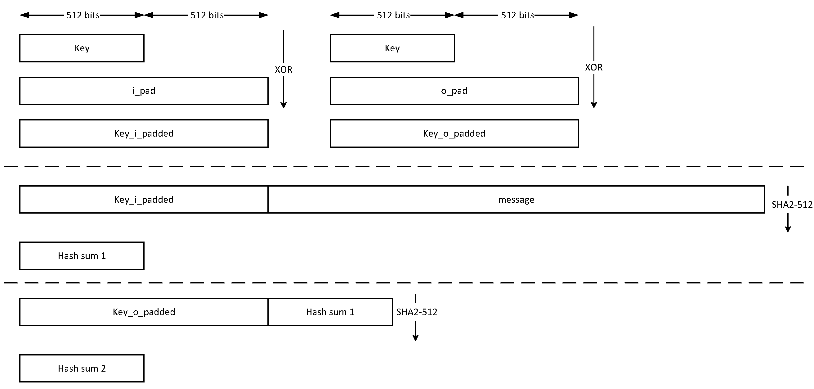
The HMAC512 core performs the sha2-512 function to process the hash value of the given message. The algorithm processes each block of the 1024 bits from the message, using the result from the previous block. This data flow is shown in the following figure.
Figure 28: HMAC-SHA-512-256 data flow
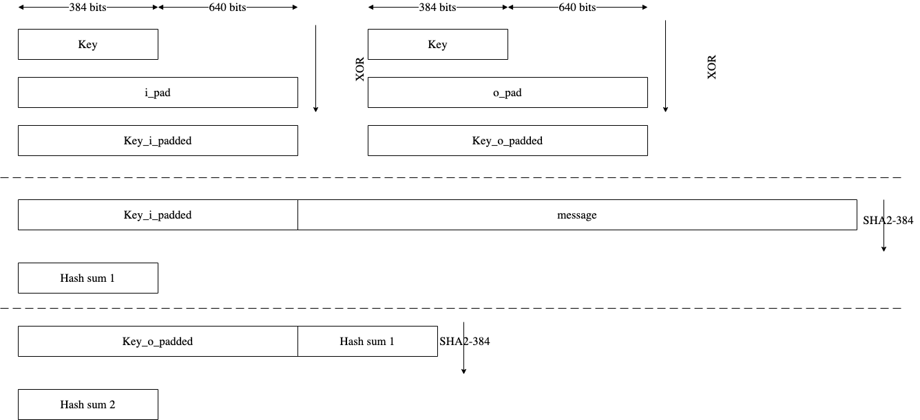
The HMAC384 core performs the sha2-384 function to process the hash value of the given message. The algorithm processes each block of the 1024 bits from the message, using the result from the previous block. This data flow is shown in the following figure.
Figure 29: HMAC-SHA-384-192 data flow
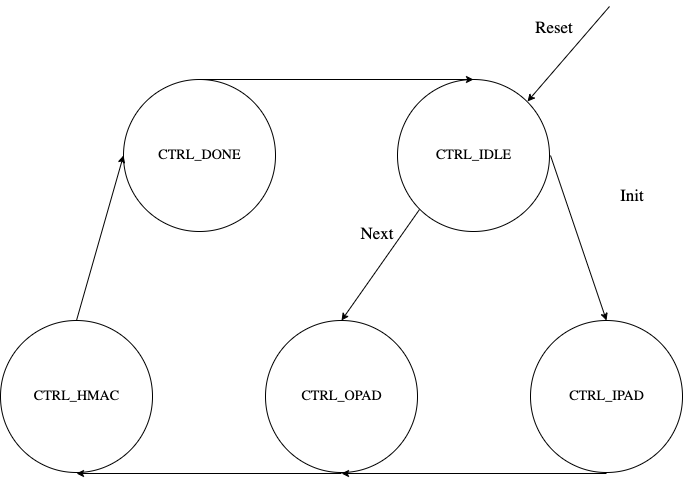
FSM
The HMAC architecture has the finite-state machine as shown in the following figure.
Figure 30: HMAC FSM
CSR Mode
When the CSR Mode register is set, the HMAC512 core uses the value latched from the cptra_csr_hmac_key interface pins in place of the API key register. These pins are latched internally after powergood assertion during DEVICE_MANUFACTURING lifecycle state. During debug mode operation this value is overridden with all 1's, and during any other lifecycle state it has a value of zero.
Signal descriptions
The HMAC architecture inputs and outputs are described in the following table.
| Name | Input or output | Description |
|---|---|---|
| clk | input | All signal timings are related to the rising edge of clk. |
| reset_n | input | The reset signal is active LOW and resets the core. This is the only active LOW signal. |
| init | input | The core is initialized and processes the key and the first block of the message. |
| next | input | The core processes the rest of the message blocks using the result from the previous blocks. |
| zeroize | input | The core clears all internal registers to avoid any SCA information leakage. |
| csr_mode | input | When set, the key comes from the cptra_csr_hmac_key interface pins. This key is valid only during MANUFACTURING mode. |
| mode | input | Indicates the hmac type of the function. This can be: - HMAC384 - HMAC512. |
| cptra_csr_hmac_key[511:0] | input | The key to be used during csr mode. |
| key[511:0] | input | The input key. |
| block[1023:0] | input | The input padded block of message. |
| LFSR_seed[383:0] | Input | The input to seed PRNG to enable the masking countermeasure for SCA protection. |
| ready | output | When HIGH, the signal indicates the core is ready. |
| tag[511:0] | output | The HMAC value of the given key or block. For PRF-HMAC-SHA-512, a 512-bit tag is required. For HMAC-SHA-512-256, the host is responsible for reading 256 bits from the MSB. |
| tag_valid | output | When HIGH, the signal indicates the result is ready. |
Address map
The HMAC address map is shown here: hmac_reg — clp Reference (chipsalliance.github.io).
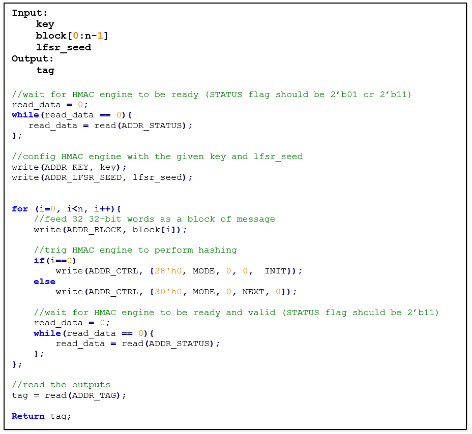
Pseudocode
The following pseudocode demonstrates how the HMAC interface can be implemented.
Figure 31: HMAC pseudocode
SCA countermeasure
In an attack model, an attacker can form hypotheses about the secret key value and compute the corresponding output values by using the Hamming Distance model as an appropriate leakage model. An attacker who has knowledge of the implementation for open-source architecture has an advantage. The attacker can capture the power consumption traces to verify their hypotheses, by partitioning the acquisitions or using Pearson’s correlation coefficient.
To protect the HMAC algorithm from side-channel attacks, a masking countermeasure is applied. This means that random values are added to the intermediate variables during the algorithm’s execution, so that the side-channel signals do not reveal any information about them.
The embedded countermeasures are based on "Differential Power Analysis of HMAC Based on SHA-2, and Countermeasures" by McEvoy et. al. To provide the required random values for masking intermediate values, a lightweight 74-bit LFSR is implemented. Based on “Spin Me Right Round Rotational Symmetry for FPGA-specific AES” by Wegener et. al., LFSR is sufficient for masking statistical randomness.
Each round of SHA512 execution needs 6,432 random bits, while one HMAC operation needs at least 4 rounds of SHA512 operations. However, the proposed architecture requires only 384-bit LFSR seed and provides first-order DPA attack protection at the cost of 10% latency overhead with negligible hardware resource overhead.
Performance
The HMAC core performance is reported considering two different architectures: pure hardware architecture, and hardware/software architecture. These are described next.
Pure hardware architecture
In this architecture, the HMAC interface and controller are implemented in hardware. The performance specification of the HMAC architecture is reported as shown in the following table.
| Operation | Cycle count [CCs] | Time [us] @ 400 MHz | Throughput [op/s] |
|---|---|---|---|
| Data_In transmission | 44 | 0.11 | - |
| Process | 254 | 0.635 | - |
| Data_Out transmission | 12 | 0.03 | - |
| Single block | 310 | 0.775 | 1,290,322 |
| Double block | 513 | 1.282 | 780,031 |
| 1 KiB message | 1,731 | 4.327 | 231,107 |
| 128 KiB message | 207,979 | 519.947 | 1,923 |
Hardware/software architecture
In this architecture, the HMAC interface and controller are implemented in RISC-V core. The performance specification of the HMAC architecture is reported as shown in the following table.
| Operation | Cycle count [CCs] | Time [us] @ 400 MHz | Throughput [op/s] |
|---|---|---|---|
| Data_In transmission | 1389 | 3.473 | - |
| Process | 253 | 0.633 | - |
| Data_Out transmission | 290 | 0.725 | - |
| Single block | 1932 | 4.83 | 207,039 |
| Double block | 3166 | 7.915 | 136,342 |
| 1 KiB message | 10,570 | 26.425 | 37,842 |
| 128 KiB message | 1,264,314 | 3,160.785 | 316 |
HMAC_DRBG
Hash-based message authentication code (HMAC) deterministic random bit generator (DRBG) is a cryptographic random bit generator that uses a HMAC function. HMAC_DRBG involves a cryptographic HMAC function and a seed. This architecture is designed as specified in section 10.1.2. of NIST SP 800-90A [12]. For ECC signing operation, the implementation is compatible with section 3.1. of RFC 6979 [7].
Caliptra HMAC_DRBG implementation uses HMAC384 as the HMAC function, accepts a 384-bit seed, and generates a 384-bit random value.
The HMAC algorithm is described as follows:
- The seed is fed to HMAC_DRBG core by the host
- For each 384-bit random value
- The core should be triggered by the host
- The HMAC_DRBG core status is changed to ready after HMAC processing
- The result digest can be read
Operation
HMAC_DRBG uses a loop of HMAC(K, V) to generate the random bits. In this algorithm, two constant values of K_init and V_init are used as follows:
        1. 	Set V_init = 0x01 0x01 0x01 ... 0x01  (V has 384-bit)
        2. 	Set K_init = 0x00 0x00 0x00 ... 0x00  (K has 384-bit)
        3. 	K_tmp = HMAC(K_init, V_init || 0x00 || entropy || nonce)
        4. 	V_tmp = HMAC(K_tmp,  V_init)
        5. 	K_new = HMAC(K_tmp,  V_tmp  || 0x01 || entropy || nonce)
        6. 	V_new = HMAC(K_new,  V_tmp)
        7. 	Set T = []
        8. 	T = T || HMAC(K_new, V_new)
        9. 	Return T if T is within the [1,q-1] range, otherwise:
        10.	K_new = HMAC(K_new,  V_new || 0x00)
        11.	V_new = HMAC(K_new,  V_new)
        12.	Jump to 8
For ECC KeyGen operation, HMAC_DRBG is used to generate privkey as follows:
Privkey = HMAC_DRBG(seed, nonce)
For ECC SIGNING operation, HMAC_DRBG is used to generate k as follows:
K = HMAC_DRBG(privkey, hashed_msg)
Signal descriptions
The HMAC_DRBG architecture inputs and outputs are described in the following table.
| Name | Input or output | Description |
|---|---|---|
| clk | input | All signal timings are related to the rising edge of clk. |
| reset_n | input | The reset signal is active LOW and resets the core. This is the only active LOW signal. |
| init | input | The core is initialized with the given seed and generates a 384-bit random value. |
| next | input | The core generates a new 384-bit random value using the result from the previous run. |
| zeroize | input | The core clears all internal registers to avoid any SCA information leakage. |
| entropy [383:0] | input | The input entropy. |
| nonce [383:0] | input | The input nonce. |
| LFSR_seed [147 :0] | input | The input to seed PRNG to enable masking countermeasure for SCA protection. |
| ready | output | When HIGH, the signal indicates the core is ready. |
| drbg [383:0] | output | The hmac_drbg value of the given inputs. |
| valid | output | When HIGH, the signal indicates the result is ready. |
Address map
The HMAC_DRBG is embedded into ECC architecture, since there is no address map to access it from FW.
SCA countermeasure
For information, see SCA countermeasure in the HMAC384 section.
ECC
The ECC unit includes the ECDSA (Elliptic Curve Digital Signature Algorithm) engine and the ECDH (Elliptic Curve Diffie-Hellman Key-Exchange) engine, offering a variant of the cryptographically secure Digital Signature Algorithm (DSA) and Diffie-Hellman Key-Exchange (DH), which uses elliptic curve (ECC). A digital signature is an authentication method in which a public key pair and a digital certificate are used as a signature to verify the identity of a recipient or sender of information.
The hardware implementation supports deterministic ECDSA, 384 Bits (Prime Field), also known as NIST-Secp384r1, described in RFC6979.
The hardware implementation also supports ECDH, 384 Bits (Prime Field), also known as NIST-Secp384r1, described in SP800-56A.
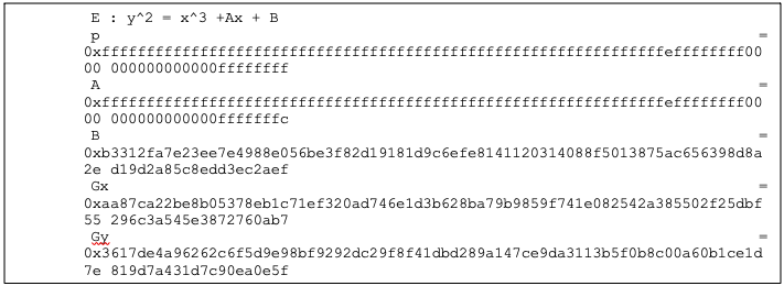
Secp384r1 parameters are shown in the following figure.
Figure 32: Secp384r1 parameters
Operation
The ECDSA consists of three operations, shown in the following figure.
Figure 33: ECDSA operations
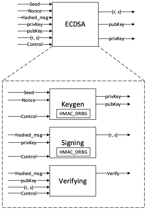
The ECDH also consists of the sharedkey generation.
KeyGen
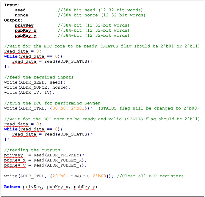
In the deterministic key generation, the paired key of (privKey, pubKey) is generated by KeyGen(seed, nonce), taking a deterministic seed and nonce. The KeyGen algorithm is as follows:
- Compute privKey = HMAC_DRBG(seed, nonce) to generate a random integer in the interval [1, n-1] where n is the group order of Secp384 curve.
- Generate pubKey(x,y) as a point on ECC calculated by pubKey=privKey × G, while G is the generator point over the curve.
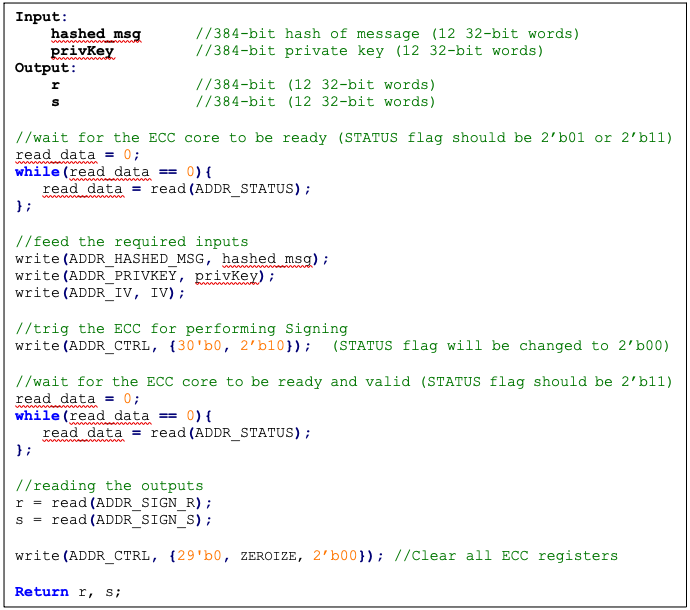
Signing
In the signing algorithm, a signature (r, s) is generated by Sign(privKey, h), taking a privKey and hash of message m, h = hash(m), using a cryptographic hash function, SHA512. The signing algorithm includes:
- Generate a random number k in the range [1..n-1], while k = HMAC_DRBG(privKey, h)
- Calculate the random point R = k × G
- Take r = Rx mod n, where Rx is x coordinate of R=(Rx, Ry)
- Calculate the signature proof: s = k-1 × (h + r × privKey) mod n
- Return the signature (r, s), each in the range [1..n-1]
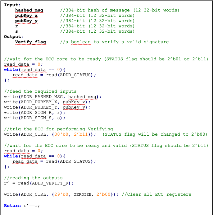
Verifying
The signature (r, s) can be verified by Verify(pubKey ,h ,r, s) considering the public key pubKey and hash of message m, h=hash(m) using the same cryptographic hash function SHA512. The output is r’ value of verifying a signature. The ECDSA verify algorithm includes:
- Calculate s1 = s−1 mod n
- Compute R' = (h × s1) × G + (r × s1) × pubKey
- Take r’ = R'x mod n, while R'x is x coordinate of R’=(R'x, R'y)
- Verify the signature by comparing whether r' == r
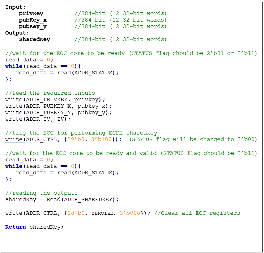
ECDH sharedkey
In ECDH sharedkey generation, the shared key is generated by ECDH_sharedkey(privKey_A, pubKey_B), taking an own prikey and other party pubkey. The ECDH sharedkey algorithm is as follows:
- Compute P = sharedkey(privkey_A, pubkey_b) where P(x,y) is a point on ECC.
- Output sharedkey = Px, where Px is x coordinate of P.
Architecture
The ECC top-level architecture is shown in the following figure.
Figure 34: ECC architecture
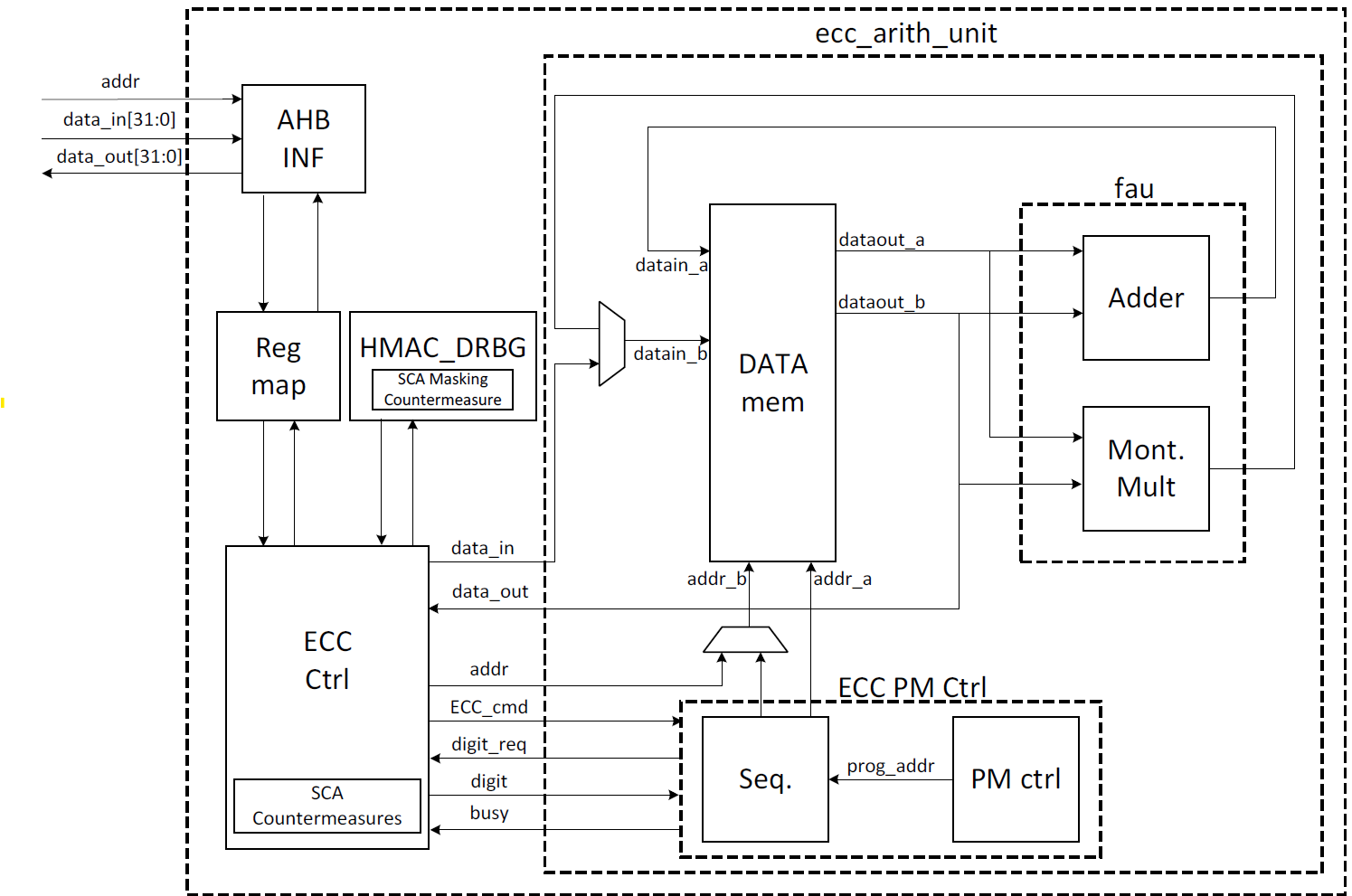
Signal descriptions
The ECC architecture inputs and outputs are described in the following table.
| Name | Input or output | Description |
|---|---|---|
| clk | input | All signal timings are related to the rising edge of clk. |
| reset_n | input | The reset signal is active LOW and resets the core. This is the only active LOW signal. |
| ctrl[1:0] | input | Indicates the AES type of the function. This can be: − 0b00: No Operation − 0b01: KeyGen − 0b10: Signing − 0b11: Verifying |
| zeroize | input | The core clears all internal registers to avoid any SCA information leakage. |
| seed [383:0] | input | The deterministic seed for HMAC_DRBG in the KeyGen operation. |
| nonce [383:0] | input | The deterministic nonce for HMAC_DRBG in the KeyGen operation. |
| privKey_in[383:0] | input | The input private key used in the signing operation. |
| pubKey_in[1:0][383:0] | input | The input public key(x,y) used in the verifying operation. |
| hashed_msg[383:0] | input | The hash of message using SHA512. |
| ready | output | When HIGH, the signal indicates the core is ready. |
| privKey_out[383:0] | output | The generated private key in the KeyGen operation. |
| pubKey_out[1:0][383:0] | output | The generated public key(x,y) in the KeyGen operation. |
| r[383:0] | output | The signature value of the given priveKey/message. |
| s[383:0] | output | The signature value of the given priveKey/message. |
| r’[383:0] | Output | The signature verification result. |
| DH_sharedkey[383:0] | output | The generated shared key in the ECDH sharedkey operation. |
| valid | output | When HIGH, the signal indicates the result is ready. |
Address map
The ECC address map is shown here: ecc_reg — clp Reference (chipsalliance.github.io).
Pseudocode
The following pseudocode blocks demonstrate example implementations for KeyGen, Signing, Verifying, and ECDH sharedkey.
KeyGen
Figure 35: KeyGen pseudocode
Signing
Figure 36: Signing pseudocode
Verifying
Figure 37: Verifying pseudocode
ECDH sharedkey
Figure 38: ECDH sharedkey pseudocode
SCA countermeasure
The described ECC has four main routines: KeyGen, Signing, Verifying, and ECDH sharedkey. Since the Verifying routine requires operation with public values rather than a secret value, our side-channel analysis does not cover this routine. Our evaluation covers the KeyGen, Signing, and ECDH sharedkey routines where the secret values are processed.
KeyGen consists of HMAC DRBG and scalar multiplication, while Signing first requires a message hashing and then follows the same operations as KeyGen (HMAC DRBG and scalar multiplication). The last step of Signing is generating “S” as the proof of signature. Since HMAC DRBG and hash operations are evaluated separately in our document, this evaluation covers scalar multiplication and modular arithmetic operations.
Scalar multiplication
To perform the scalar multiplication, the Montgomery ladder is implemented, which is inherently resistant to timing and single power analysis (SPA) attacks.
Implementation of complete unified addition formula for the scalar multiplication avoids information leakage and enhances architecture from security and mathematical perspectives.
To protect the architecture against horizontal power/electromagnetic (EM) and differential power analysis (DPA) attacks, several countermeasures are embedded in the design [9]. Since these countermeasures require random inputs, HMAC-DRBG is fed by IV to generate these random values.
Since HMAC-DRBG generates random value in a deterministic way, firmware MUST feed different IV to ECC engine for EACH keygen, signing, and ECDH sharedkey operation.
Base point randomization
This countermeasure is achieved using the randomized base point in projective coordinates. Hence, the base point G=(Gx, Gy) in affine coordinates is transformed and randomized to projective coordinates as (X, Y, Z) using a random value as follows:
This approach does not have the performance or area overhead because the architecture is variable-base-point implemented.
Scalar blinding
This countermeasure is achieved by randomizing the scalar as follows:
Based on [10], half of the bit size of is required to prevent advanced DPA attacks. Therefore, has 192 bits, and the blinded scalar has 576 bits. Hence, this countermeasure extends the Montgomery ladder iterations due to extended scalar.
This approach is achieved at the cost of 50% more latency on scalar multiplication and adding one lightweight block, including one 32*32 multiplier and an accumulator.
Note: the length of rand is configurable to have a trade-off between the required protection and performance.
Making countermeasures embedded into HMAC_DRBG
In the first step of the KeyGen operation, the privkey is generated using HMAC_DRBG by feeding the following two inputs: seed and nonce. To avoid SCA information leakage during this operation, we embed masking countermeasures into the HMAC_DRBG architecture.
Each round of SHA512 execution needs 6,432 random bits, and one HMAC operation needs at least 4 rounds of SHA512 operations. Furthermore, each HMAC_DRBG round needs at least 5 rounds of HMAC operations. However, the proposed architecture uses a lightweight LFSR and provides first-order DPA attack protection with negligible latency and hardware resource overhead.
ECDSA signing nonce leakage
Generating “S” as the proof of signature at the steps of the signing operation leaks where the hashed message is signed with private key and ephemeral key as follows:
Since the given message is known or the signature part r is known, the attacker can perform a known-plaintext attack. The attacker can sign multiple messages with the same key, or the attacker can observe part of the signature that is generated with multiple messages but the same key.
The evaluation shows that the CPA attack can be performed with a small number of traces, respectively. Thus, an arithmetic masked design for these operations is implemented.
Masking signature
This countermeasure is achieved by randomizing the privkey as follows:
Although computation of “S” seems the most vulnerable point in our scheme, the operation does not have a big contribution to overall latency. Hence, masking these operations has low overhead on the cost of the design.
Random number generator for SCA countermeasure
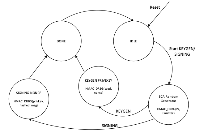
The ECC countermeasure requires several random vectors to randomize the intermediate values, as described in the preceding section. HMAC_DRBG is used to take one random vector of 384-bit (i.e., ECC_IV register) and to generate the required random vectors for different countermeasures.
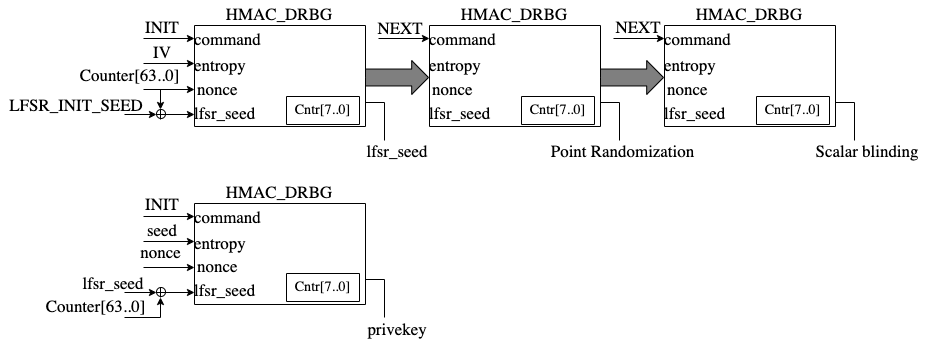
The state machine of HMAC_DRBG utilization is shown in the following figure, including three main states:
- SCA random generator: Running HMAC_DRBG with IV and an internal counter to generate the required random vectors.
- KEYGEN PRIVKEY: Running HMAC_DRBG with seed and nonce to generate the privkey in KEYGEN operation.
- SIGNING NONCE: Running HMAC_DRBG based on RFC6979 in SIGNING operation with privkey and hashed_msg.
Figure 39: HMAC_DRBG utilization
In SCA random generator state:
- This state (in KeyGen operation mode) generates 3 384-bit random vectors for the following: LFSR, base point randomization, and scalar blinding randomization.
- This state (in signing operation) generates 4 384-bit random vectors for the following: LFSR, base point randomization, scalar blinding, and masking signature randomization.
- HMAC_DRBG is initialized with IV and an internal counter. This 64-bit counter enables after reset and zeroization and contains different values depending on when ECC is called.
- HMAC_DRBG is enabled by the INIT command. To generate all required vectors, HMAC-DRBG is continued by the NEXT command that increments the built-in counter inside the HMAC-DRBG unit.
- To initialize the required seed for LFSR, LFSR_INIT_SEED is set as a constant by RTL after reset and zeroization. However, this value is updated before enabling HMAC_DRBG as follows:
- In the first execution of HMAC_DRBG after reset and zeroization, hmac_lfsr_seed is equal to LFSR_INIT_SEED XORed by internal 64-bit counter.
- In the next executions of HMAC_DRBG, hmac_lfsr_seed is equal to HMAC_DRBG output of the first execution XORed by internal 64-bit counter.
The data flow of the HMAC_DRBG operation in keygen operation mode is shown in the following figure.
Figure 40: HMAC_DRBG data flow
TVLA results
Test vector leakage assessment (TVLA) provides a robust test using a 𝑡-test. This test evaluates the differences between sets of acquisitions to determine if one set of measurement can be distinguished from the other. This technique can detect different types of leakages, providing a clear indication of leakage or lack thereof.
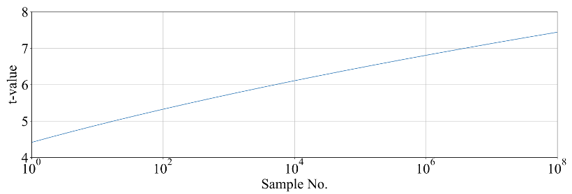
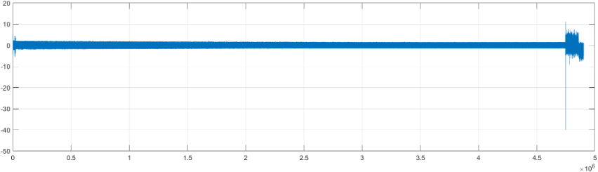
In practice, observing a t-value greater than a specific threshold (mainly 4.5) indicates the presence of leakage. However, in ECC, due to its latency, around 5 million samples are required to be captured. This latency leads to many false positives and the TVLA threshold can be considered a higher value than 4.5. Based on the following figure from “Side-Channel Analysis and Countermeasure Design for Implementation of Curve448 on Cortex-M4” by Bisheh-Niasar et. al., the threshold can be considered equal to 7 in our case.
Figure 41: TVLA threshold as a function of the number of samples per trace
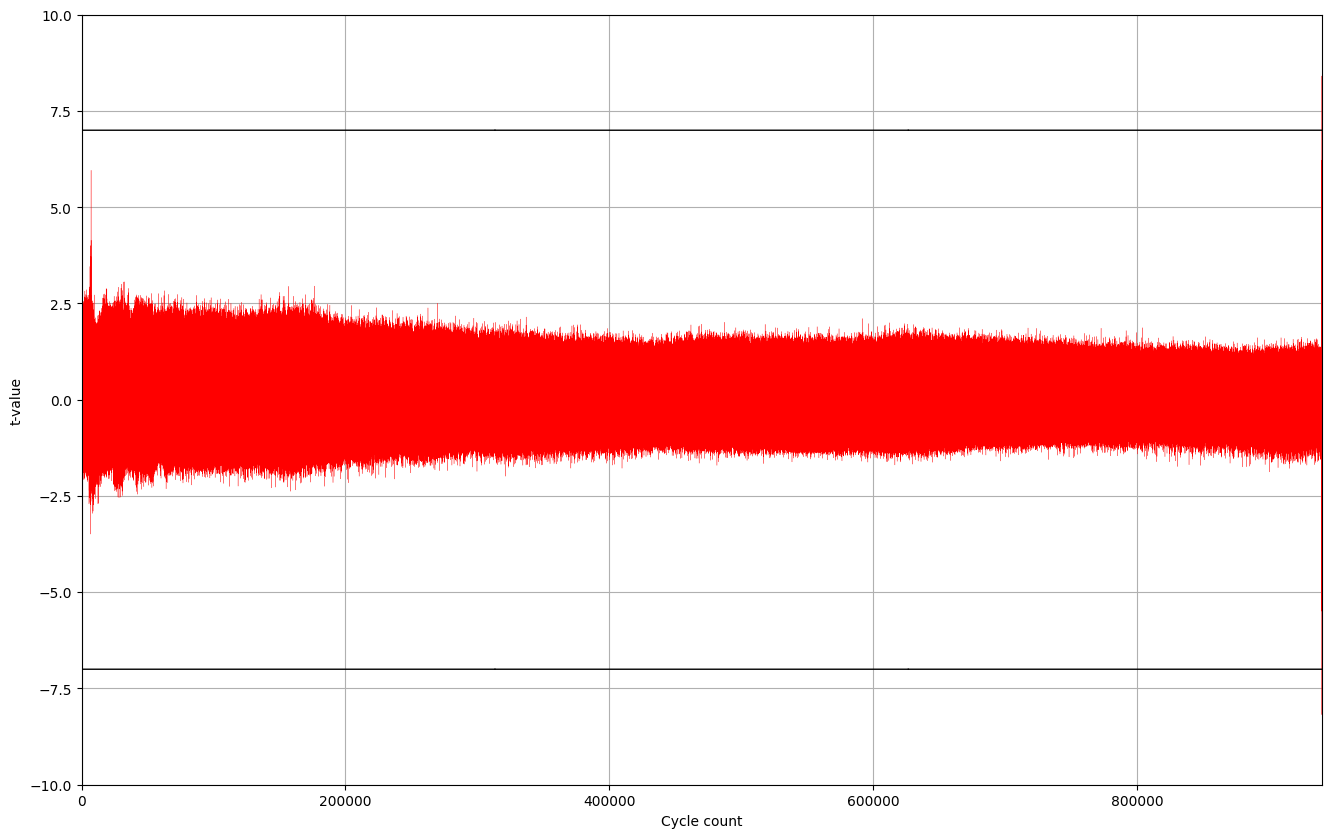
KeyGen TVLA
The TVLA results for performing seed/nonce-dependent leakage detection using 200,000 traces is shown in the following figure. Based on this figure, there is no leakage in ECC keygen by changing the seed/nonce after 200,000 operations.
Figure 42: seed/nonce-dependent leakage detection using TVLA for ECC keygen after 200,000 traces
Signing TVLA
The TVLA results for performing privkey-dependent leakage detection using 20,000 traces is shown in the following figure. Based on this figure, there is no leakage in ECC signing by changing the privkey after 20,000 operations.
Figure 43: privkey-dependent leakage detection using TVLA for ECC signing after 20,000 traces
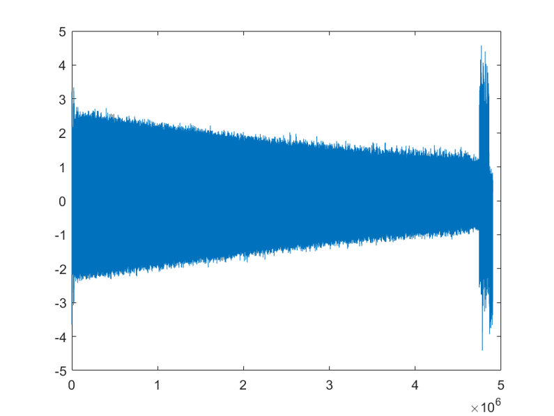
The TVLA results for performing message-dependent leakage detection using 64,000 traces is shown in the following figure. Based on this figure, there is no leakage in ECC signing by changing the message after 64,000 operations.
Figure 44: Message-dependent leakage detection using TVLA for ECC signing after 64,000 traces
The point with t-value equal to -40 is mapped to the Montgomery conversion of the message that is a publicly known value (no secret is there). By ignoring those corresponding samples, there are some sparse samples with a t-value greater than 7, as shown in the following table.
| Sample | Duration | Cycle | t-value | Operation |
|---|---|---|---|---|
| 4,746,127 | 214 | 911,381.4 | 11.2 | start of mont_conv(msg) |
| 4,746,341 | 911,422.5 | -40 | end of mont_conv(msg) | |
| 4,757,797 | 1 | 913,622.0 | 7.4 | inv_q |
| 4,768,302 | 1 | 915,639.0 | 7.8 | inv_q |
| 4,779,610 | 1 | 917,810.1 | -9.1 | inv_q |
| 4,788,120 | 1 | 919,444.0 | 7.6 | inv_q |
| 4,813,995 | 1 | 924,412.0 | 7.3 | inv_q |
| 4,822,693 | 1 | 926,082.1 | 7.5 | inv_q |
| 4,858,671 | to the end | 932,989.8 | -7.6 | Ended ECC signing |
Performance
The ECC core performance is reported in the next section.
Pure hardware architecture
In this architecture, the ECC interface and controller are implemented in hardware. The performance specification of the ECC architecture is reported as shown in the following table.
| Operation | Cycle count [CCs] | Time [ms] @ 400 MHz | Throughput [op/s] |
|---|---|---|---|
| Keygen | 909,648 | 2.274 | 439 |
| Signing | 932,990 | 2.332 | 428 |
| Verifying | 1,223,938 | 3.060 | 326 |
LMS Accelerator
LMS cryptography is a type of hash-based digital signature scheme that was standardized by NIST in 2020. It is based on the Leighton-Micali Signature (LMS) system, which uses a Merkle tree structure to combine many one-time signature (OTS) keys into a single public key. LMS cryptography is resistant to quantum attacks and can achieve a high level of security without relying on large integer mathematics.
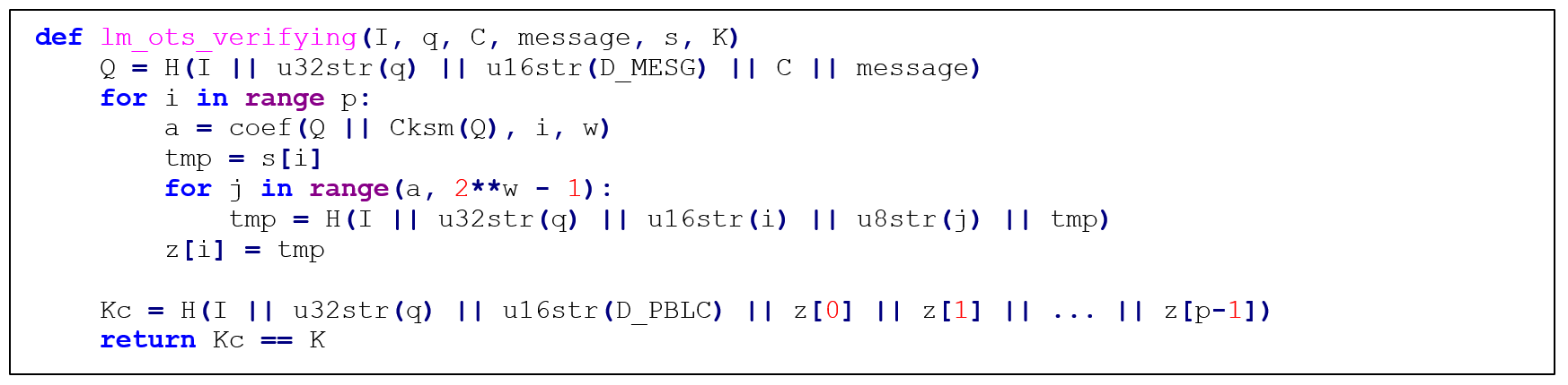
Caliptra supports only LMS verification using a software/hardware co-design approach. Hence, the LMS accelerator reuses the SHA256 engine to speedup the Winternitz chain by removing software-hardware interface overhead. The LMS-OTS verification algorithm is shown in follwoing figure:
Figure 45: LMS-OTS Verification algorithm
The high-level architecture of LMS is shown in the following figure.
Figure 46: LMS high-level architecture
LMS parameters
LMS parameters are shown in the following table:
| Parameter | Description | Value |
|---|---|---|
| n | The number of bytes of the output of the hash function. | {24, 32} |
| w | The width (in bits) of the Winternitz coefficients. | {1, 2, 4, 8} |
| p | The number of n-byte string elements that make up the LM-OTS signature. | {265, 133, 67, 34} |
| H | A cryptographic hash function. | SHA256 |
| h | The height of the tree. | {5, 10, 15, 20, 25} |
- SHA256 is used for n=32 and SHA256/192 is used for n=24.
- SHAKE256 is not supported in this architecture.
- Value of p is determined based on w. If w=1, p is equal to 265, and so on.
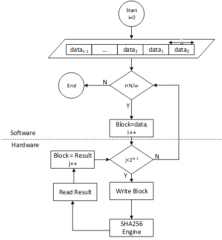
Winternitz Chain Accelerator
The Winternitz hash chain can be accelerated in hardware to enhance the performance of the design. For that, a configurable architecture is proposed that can reuse SHA256 engine. The LMS accelerator architecture is shown in the following figure, while H is SHA256 engine.
Figure 47: Winternitz chain architecture
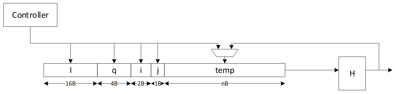
Signal descriptions
The LMS accelerator integrated into SHA256 architecture inputs and outputs are described as follows.
| Name | Input or output | Description |
|---|---|---|
| clk | input | All signal timings are related to the rising edge of clk. |
| reset_n | input | The reset signal is active LOW and resets the core. This is the only active LOW signal. |
| init | input | The core is initialized and processes the first block of message. |
| next | input | The core processes the rest of the message blocks using the result from the previous blocks. |
| mode | input | Indicates the hash type of the function. This can be: - SHA256/224 - SHA256 |
| zeroize | input | The core clears all internal registers to avoid any SCA information leakage. |
| WNTZ_MODE | input | SHA256 core is configured in Winternitz verification mode. |
| WNTZ_W[3:0] | input | Winternitz W value. |
| WNTZ_N_MODE | input | Winternitz n value(SHA192/SHA256 --> n = 24/32) |
| block[511:0] | input | The input padded block of message. |
| ready | output | When HIGH, the signal indicates the core is ready. |
| digest[255:0] | output | The hashed value of the given block. |
| digest_valid | output | When HIGH, the signal indicates the result is ready. |
Address map
The address map for LMS accelerator integrated into SHA256 is shown here: sha256_reg — clp Reference (chipsalliance.github.io).
Adams Bridge - Dilithium (ML-DSA)
Please refer to the Adams-bridge specification
Address map
Address map of ML-DSA accelerator is shown here: ML-DSA_reg — clp Reference (chipsalliance.github.io)
AES
The AES unit is a cryptographic accelerator that processes requests from the processor to encrypt or decrypt 16-byte data blocks. It supports AES-128/192/256 in various modes, including Electronic Codebook (ECB), Cipher Block Chaining (CBC), Cipher Feedback (CFB) with a fixed segment size of 128 bits (CFB-128), Output Feedback (OFB), Counter (CTR), and Galois/Counter Mode (GCM).
The AES unit is reused from here, (see aes with a shim to translate from AHB-lite to the tl-ul interface.
Additional registers have been added to support key vault integration. Keys from the key vault can be loaded into the AES unit to be used for encryption or decryption.
Operation
For more information, see the AES Programmer's Guide.
Signal descriptions
The AES architecture inputs and outputs are described in the following table.
| Name | Input or output | Description |
|---|---|---|
| clk | input | All signal timings are related to the rising edge of clk. |
| reset_n | input | The reset signal is active LOW and resets the core. This is the only active LOW signal. |
| DATA_IN | input | Input block to be encrypted or decrypted. Written in four 32-bit registers. |
| DATA_OUT | output | Output block result of encryption or decryption. Stored in four 32-bit registers. |
| CTRL_SHADOWED.MANUAL_OPERATION | input | Configures the AES core to operation in manual mode. |
| CTRL_SHADOWED.PRNG_RESEED_RATE | input | Configures the rate of reseeding the internal PRNG used for masking. |
| CTRL_SHADOWED.SIDELOAD | input | When asserted, AES core will use the key from the keyvault interface. |
| CTRL_SHADOWED.KEY_LEN | input | Configures the AES key length. Supports 128, 192, and 256-bit keys. |
| CTRL_SHADOWED.MODE | input | Configures the AES block cipher mode. |
| CTRL_SHADOWED.OPERATION | input | Configures the AES core to operate in encryption or decryption modes. |
| CTRL_GCM_SHADOWED.PHASE | input | Configures the GCM phase. |
| CTRL_GCM_SHADOWED.NUM_VALID_BYTES | input | Configures the number of valid bytes of the current input block in GCM. |
| TRIGGER.PRNG_RESEED | input | Forces a PRNG reseed. |
| TRIGGER.DATA_OUT_CLEAR | input | Clears the DATA_OUT registers with pseudo-random data. |
| TRIGGER.KEY_IV_DATA_IN_CLEAR | input | Clears the Key, IV, and DATA_INT registers with pseudo-random data. |
| TRIGGER.START | input | Triggers the encryption/decryption of one data block if in manual operation mode. |
| STATUS.ALERT_FATAL_FAULT | output | A fatal fault has ocurred and the AES unit needs to be reset. |
| STATUS.ALERT_RECOV_CTRL_UPDATE_ERR | output | An update error has occurred in the shadowed Control Register. AES operation needs to be restarted by re-writing the Control Register. |
| STATUS.INPUT_READY | output | The AES unit is ready to receive new data input via the DATA_IN registers. |
| STATUS.OUTPUT_VALID | output | The AES unit has alid output data. |
| STATUS.OUTPUT_LOST | output | All previous output data has been fully read by the processor (0) or at least one previous output data block has been lost (1). It has been overwritten by the AES unit before the processor could fully read it. Once set to 1, this flag remains set until AES operation is restarted by re-writing the Control Register. The primary use of this flag is for design verification. This flag is not meaningful if MANUAL_OPERATION=0. |
| STATUS.STALL | output | The AES unit is stalled because there is previous output data that must be read by the processor before the AES unit can overwrite this data. This flag is not meaningful if MANUAL_OPERATION=1. |
| STATUS.IDLE | output | The AES unit is idle. |
Address map
The AES address map is shown here: aes_clp_reg — clp Reference (chipsalliance.github.io).
SCA countermeasures
The AES unit employs separate SCA countermeasures for the AES cipher core used for the encryption/decryption part and for the GHASH module used for computing the integrity tag in GCM.
AES cipher core
A detailed specification of the SCA countermeasure employed in the AES cipher core is shown here: AES cipher core SCA countermeasure. The most critical building block of the SCA countermeasure, i.e., the masked AES S-Box, successfully passes formal masking verification at the netlist level using Alma: Execution-aware Masking Verification. The flow required for repeating the formal masking verification using Alma together with a Howto can be found here. The entire AES cipher core including the masked S-Boxes and as well as the PRNG generating the randomness for remasking successfully passes masking evaluation at the netlist level using PROLEAD - A Probing-Based Leakage Detection Tool for Hardware and Software. The flow required for repeating the masking evaluation using PROLEAD together with a Howto can be found here.
GHASH module
A detailed specification of the SCA countermeasure employed in the GHASH module is shown here: GHASH module SCA countermeasure.
To optimize and verify this masking countermeasure, two different types of experiments have been performed for which the results are given below.
- Formal masking verification using Alma: Execution-aware Masking Verification. These experiments led to a series of small design optimizations which have been integrated into Caliptra. The resulting design successfully passes formal masking verification at the netlist level.
- Test-vector leakage assessment (TVLA) applied to power SCA traces captured on a ChipWhisperer-based FPGA setup. These experiments confirm the formal masking verification results: No 1st-order SCA can be observed during the GHASH operation. The leakage observed at the boundary of and outside the GHASH operation can be attributed to the evaluation methodology and the handling of unmasked and uncritical data, as well as to FPGA-specific leakage effects known from literature. We are confident that the optimized SCA hardening concept effectively deters SCA attacks.
Formal masking verification using Alma
Alma is an open source, formal masking verification tool developed at TU Graz which enables formal verification of masking SCA countermeasures at the netlist level. The main advantages of this approach compared to analyzing FPGA power traces are as follows:
- The turn-around time is much faster as it does not involve FPGA bitstream generation and capturing power traces (both can take several hours).
- Netlist-based analysis tools typically enable pinpointing sources of SCA leakage and easily allow analyzing sub parts of the masked design individually. As a result, individual issues can be fixed up faster.
- The analyzed netlist is closer to the targeted ASIC implementation. During FPGA synthesis, the netlist is mapped to the logic elements such as look-up tables (LUTs) available on the selected FPGA which are fundamentally different from more simple ASIC gates.
However, formal netlist analysis tools may not be perfect and they also have limitations in terms of what can be analyzed. For example, the maximum supported netlist size depends on the complexity and number of the non-linear elements. Also, random number generators and in particular pseudo-random number generators typically need to be excluded from the analysis and random number inputs need to be assumed as ideal by tools. Thus, they don’t replace FPGA-based analysis. We use them to increase our confidence in our SCA countermeasures and to close countermeasure verification faster by reducing the number of FPGA evaluation runs.
Prerequisites
The Alma-based formal masking verification flow together with a Howto (including installation instructions) as well an open source Yosys synthesis flow are available open soure. The tool can both run on generic Yosys netlists or on proprietary and technology-specific netlists. For the latter, a slightly modified verification flow with an additional translation step is required. To verify the GHASH SCA countermeasure, the generic flow was used with the following tool versions:
- Alma (specific commit)
- Yosys 0.36 (git sha1 8f07a0d84)
- sv2v v0.0.11-28-g81d8225
- Verilator 4.214 2021-10-17 rev v4.214
Yosys Netlist Synthesis
Setup the open source Yosys synthesis flow by copying the syn_setup.example.sh file and renaming it to syn_setup.sh.
Change the LR_SYNTH_TOP_MODULE variable to aes_ghash_wrap and the LR_SYNTH_CELL_LIBRARY_PATH to the NangateOpenCellLibrary_typical.lib file in the folder where you installed the nangate45 library.
Then, start the synthesis by executing
./syn_yosys.sh
This should produce output similar to what is shown below:
8. Printing statistics.

=== aes_ghash_wrap ===

   Number of wires:             24543
   Number of wire bits:         29339
   Number of public wires:      567
   Number of public wire bits:  5363
   Number of memories:          0
   Number of memory bits:       0
   Number of processes:         0
   Number of cells:             26214
    AND2_X1                     1585
    AND3_X1                     4
    AND4_X1                     32
    AOI211_X1                   58
    AOI21_X1                    293
    AOI221_X1                   215
    AOI22_X1                    364
    DFFR_X1                     1468
    DFFS_X1                     5
    INV_X1                      584
    MUX2_X1                     1252
    NAND2_X1                    1870
    NAND3_X1                    128
    NAND4_X1                    37
    NOR2_X1                     7551
    NOR3_X1                     445
    NOR4_X1                     28
    OAI211_X1                   98
    OAI21_X1                    827
    OAI221_X1                   3
    OAI22_X1                    183
    OR2_X1                      28
    OR3_X1                      67
    OR4_X1                      2
    XNOR2_X1                    7122
    XOR2_X1                     1965

   Chip area for module '\aes_ghash_wrap': 37534.728000

====== End Yosys Stat Report ======

Warnings: 20 unique messages, 102 total

End of script. Logfile hash: 16c4d13569, CPU: user 25.11s system 0.12s, MEM: 176.29 MB peak
Yosys 0.36 (git sha1 8f07a0d84, gcc 11.4.0-1ubuntu1~22.04 -fPIC -Os)
Time spent: 66% 2x abc (47 sec), 9% 40x opt_expr (6 sec), ...
Area in kGE =  47.04
Note that the reported area is quite a bit bigger compared to the number reported in the GHASH SCA countermeasure specification The reasons are twofold:
- The
aes_ghash_wrapmodule synthesized is a wrapper module around the GHASH module in focus of this analysis. The goal of the wrapper is to separately feed in secrets (the hash subkey H and the encrypted initial counter block S) as well as randomness in a tool aware manner. As such, the wrapper includes some additional muxing resources and a counter to ease interpretation of results. - To speed up the formal analysis, the pipelined Galois-field multipliers have been instantiated with a latency of 4 instead of 32 clock cycles as on FPGA. While the latency or more precisely the processing parallelism does have an impact on the SNR, it does not have an impact on the formal netlist analysis which is performed in a so-to-say noise free environment.
Formal Netlist Analysis
After synthesizing the netlist, the following steps should be taken to perform the analysis:
-
Make sure to source the
build_consts.shscriptsource util/build_consts.shin order to set up some shell variables.
-
Enter the directory where you have downloaded Alma and load the virtual Python environment
source dev/bin/activate -
Launch the Alma tool to parse, trace (simulate) and formally verify the netlist. For simplicity, a single script is provided to launch all the required steps with a single command. Simply run
${REPO_TOP}/hw/ip/aes/pre_sca/alma/verify_aes_ghash.shThis should produce output similar to the one below:
Verifying aes_ghash_wrap using Alma
Starting yosys synthesis...
| CircuitGraph | Total: 29882 | Linear: 9091 | Non-linear: 12741 | Registers: 1473 | Mux: 3538 |
parse.py successful (47.99s)
1: Running verilator on given netlist
2: Compiling verilated netlist library
3: Compiling provided verilator testbench
4: Simulating circuit and generating VCD
| CircuitGraph | Total: 29882 | Linear: 9091 | Non-linear: 12741 | Registers: 1473 | Mux: 3538 |
tmp/tmp.vcd:24765: [WARNING] Entry for name alert_fatal_i already exists in namemap (alert_fatal_i -> Ce")
tmp/tmp.vcd:24766: [WARNING] Entry for name alert_o already exists in namemap (alert_o -> De")
tmp/tmp.vcd:24767: [WARNING] Entry for name clear_i already exists in namemap (clear_i -> Ee")
tmp/tmp.vcd:24768: [WARNING] Entry for name clk_i already exists in namemap (clk_i -> Fe")
tmp/tmp.vcd:24770: [WARNING] Entry for name cyc_ctr_o already exists in namemap (cyc_ctr_o -> Ge")
tmp/tmp.vcd:24771: [WARNING] Entry for name data_in_prev_i already exists in namemap (data_in_prev_i -> He")
tmp/tmp.vcd:24772: [WARNING] Entry for name data_out_i already exists in namemap (data_out_i -> Le")
tmp/tmp.vcd:24773: [WARNING] Entry for name first_block_o already exists in namemap (first_block_o -> Pe")
tmp/tmp.vcd:24774: [WARNING] Entry for name gcm_phase_i already exists in namemap (gcm_phase_i -> Qe")
tmp/tmp.vcd:24775: [WARNING] Entry for name ghash_state_done_o already exists in namemap (ghash_state_done_o -> Re")
tmp/tmp.vcd:24776: [WARNING] Entry for name hash_subkey_i already exists in namemap (hash_subkey_i -> Ve")
tmp/tmp.vcd:24777: [WARNING] Entry for name in_ready_o already exists in namemap (in_ready_o -> ^e")
tmp/tmp.vcd:24778: [WARNING] Entry for name in_valid_i already exists in namemap (in_valid_i -> _e")
tmp/tmp.vcd:24779: [WARNING] Entry for name load_hash_subkey_i already exists in namemap (load_hash_subkey_i -> `e")
tmp/tmp.vcd:24780: [WARNING] Entry for name num_valid_bytes_i already exists in namemap (num_valid_bytes_i -> ae")
tmp/tmp.vcd:24781: [WARNING] Entry for name op_i already exists in namemap (op_i -> be")
tmp/tmp.vcd:24782: [WARNING] Entry for name out_ready_i already exists in namemap (out_ready_i -> ce")
tmp/tmp.vcd:24783: [WARNING] Entry for name out_valid_o already exists in namemap (out_valid_o -> de")
tmp/tmp.vcd:24784: [WARNING] Entry for name prd_i already exists in namemap (prd_i -> ee")
tmp/tmp.vcd:24785: [WARNING] Entry for name rst_ni already exists in namemap (rst_ni -> me")
tmp/tmp.vcd:24786: [WARNING] Entry for name s_i already exists in namemap (s_i -> ne")
0
0
Building formula for cycle 0: vars 0 clauses 0
Checking cycle 0:
Building formula for cycle 1: vars 1024 clauses 1536
Checking cycle 1:
Building formula for cycle 2: vars 3968 clauses 6528
Checking cycle 2:
Building formula for cycle 3: vars 6298 clauses 11026
Checking cycle 3:
Building formula for cycle 4: vars 14888 clauses 34886
Checking cycle 4:
Building formula for cycle 5: vars 20924 clauses 52734
Checking cycle 5:
Building formula for cycle 6: vars 53986 clauses 143674
Checking cycle 6:
Building formula for cycle 7: vars 57570 clauses 150970
Checking cycle 7:
Building formula for cycle 8: vars 80484 clauses 169282
Checking cycle 8:
Building formula for cycle 9: vars 213770 clauses 504198
Checking cycle 9:
Building formula for cycle 10: vars 594390 clauses 1617276
Checking cycle 10:
Building formula for cycle 11: vars 1024018 clauses 2881744
Checking cycle 11:
Building formula for cycle 12: vars 1704424 clauses 4910342
Checking cycle 12:
Building formula for cycle 13: vars 1713897 clauses 4915466
Checking cycle 13:
Building formula for cycle 14: vars 1834911 clauses 5233038
Checking cycle 14:
Building formula for cycle 15: vars 2258841 clauses 6492446
Checking cycle 15:
Building formula for cycle 16: vars 2734646 clauses 7907830
Checking cycle 16:
Building formula for cycle 17: vars 5868600 clauses 18374416
Checking cycle 17:
Building formula for cycle 18: vars 5922747 clauses 18524578
Checking cycle 18:
Building formula for cycle 19: vars 6100898 clauses 19061808
Checking cycle 19:
Building formula for cycle 20: vars 6427297 clauses 20074334
Checking cycle 20:
Building formula for cycle 21: vars 6949506 clauses 21693947
Checking cycle 21:
Building formula for cycle 22: vars 6949506 clauses 21693947
Checking cycle 22:
Building formula for cycle 23: vars 6949506 clauses 21693947
Checking cycle 23:
Building formula for cycle 24: vars 7057992 clauses 21994175
Checking cycle 24:
Building formula for cycle 25: vars 7407412 clauses 23047989
Checking cycle 25:
Building formula for cycle 26: vars 7797810 clauses 24221073
Checking cycle 26:
Building formula for cycle 27: vars 10939700 clauses 34732235
Checking cycle 27:
Building formula for cycle 28: vars 11268148 clauses 35780811
Checking cycle 28:
Building formula for cycle 29: vars 11268148 clauses 35780811
Checking cycle 29:
Building formula for cycle 30: vars 11268148 clauses 35780811
Checking cycle 30:
Building formula for cycle 31: vars 11376634 clauses 36081039
Checking cycle 31:
Building formula for cycle 32: vars 11726054 clauses 37134853
Checking cycle 32:
Building formula for cycle 33: vars 12116452 clauses 38307937
Checking cycle 33:
Building formula for cycle 34: vars 15258342 clauses 48819099
Checking cycle 34:
Building formula for cycle 35: vars 15586534 clauses 49867675
Checking cycle 35:
Building formula for cycle 36: vars 15619430 clauses 49965979
Checking cycle 36:
Finished in 3948.52
The execution is secure
Notes:
-
This analysis exercises the full data path of the GHASH block and comprises the following operations (controlled by a small Verilator testbench):
- Initial clearing of all internal registers.
- Loading the hash subkey H.
- Loading the encrypted initial counter block S including the subsequent generation of repeatedly used correction terms.
- Processing a first AAD/ciphertext block including the generation of a correction term that is used for the first block only.
- Processing a second AAD/ciphertext block.
- Producing the final authentication tag.
-
The following main changes have been implemented as a result of the formal netlist analysis using Alma (refer to the countermeasure spec for details):
- The result of the final addition of Share 1 of S and the unmasked GHASH state is no longer stored into the GHASH state register but directly forwarded to the output, and the state input to this addition is blanked.
The input multiplexer (
ghash_in_mux) loses one input. - The two 3-input multiplexers selecting the operands for the addition with the GHASH state (
add_in_mux) are replaced by one-hot multiplexers with registered control signals. - The Operand B inputs of both GF multipliers are now blanked. The 3-input multiplexer selecting Operand B of the second GF multiplier is replaced by a one-hot multiplexer with registered control signal. In addition, the last input slice of Operand B for this multiplier is registered. This allows the switching the multiplexer during the last clock cycle of the multiplication to avoid some undesirable transient leakage occurring upon saving the result of the multiplication into the GHASH state register (and this new value propagating through the multiplexer into the multiplier again).
- The GF multipliers are configured to output zero instead of Operand A (the hash subkey) while busy.
- The state input for the addition required for the generation of the correction term for Share 0 is blanked.
- Between adding the correction terms to the GHASH state for the last time and between unmasking the GHASH state, a bubble cycle is added to allow signals to fully settle thereby avoiding undesirable transient effects unmasking the uncorrected state shares.
- The result of the final addition of Share 1 of S and the unmasked GHASH state is no longer stored into the GHASH state register but directly forwarded to the output, and the state input to this addition is blanked.
The input multiplexer (
-
The overall area impact of these changes is low (+0.16 kGE in Yosys + nangate45).
-
The final design successfully passes the formal masking verification. For details regarding tool parameters, check the analysis script.
ChipWhisperer-based FPGA evaluation and TVLA
To underpin the results of the formal verification flow, the hardening of the GHASH module has been analyzed on the ChipWhisperer CW310 FPGA board. For this analysis, power traces with the ChipWhisperer Husky scope were captured during GCM operations. Afterwards a Test Vector Leakage Assessment (TVLA) with the ot-sca toolset has been performed. The setup is illustrated in Figure 1.
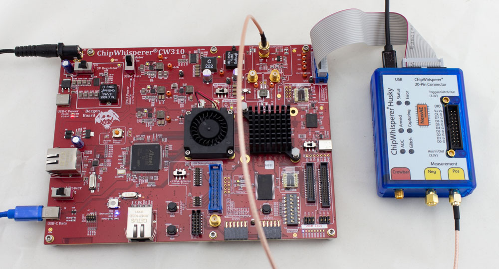 :--:
Figure 1: Target CW310 FPGA board (left) and the CW Husky scope (right).
:--:
Figure 1: Target CW310 FPGA board (left) and the CW Husky scope (right).
Setup
 :--:
Figure 2: Measurement setup. The main components are the target board, the scope, and the SCA framework.
:--:
Figure 2: Measurement setup. The main components are the target board, the scope, and the SCA framework.
Figure 2 gives a detailed overview of the measurement setup that has been utilized to capture the power traces. The SCA evaluation framework ot-sca is the central component of the measurement setup. It is responsible for communicating with the penetration testing framework that runs on the target FPGA board and with the scope. Initially, ot-sca configures the scope (sample rate, number of samples) and the pentest framework (which input, how many encryptions, where to trigger).
Based on the configuration, the pentest framework generates the cipher input, starts the encryption, and sends back the computed tag to ot-sca. The trigger is automatically set and unset by the AES hardware block to achieve an accurate & constant trigger window. In parallel, the scope waits for the trigger, captures the power consumption, and transfers the traces to the SCA evaluation framework. The ot-sca framework stores the trace as well as the cipher configuration in a database.
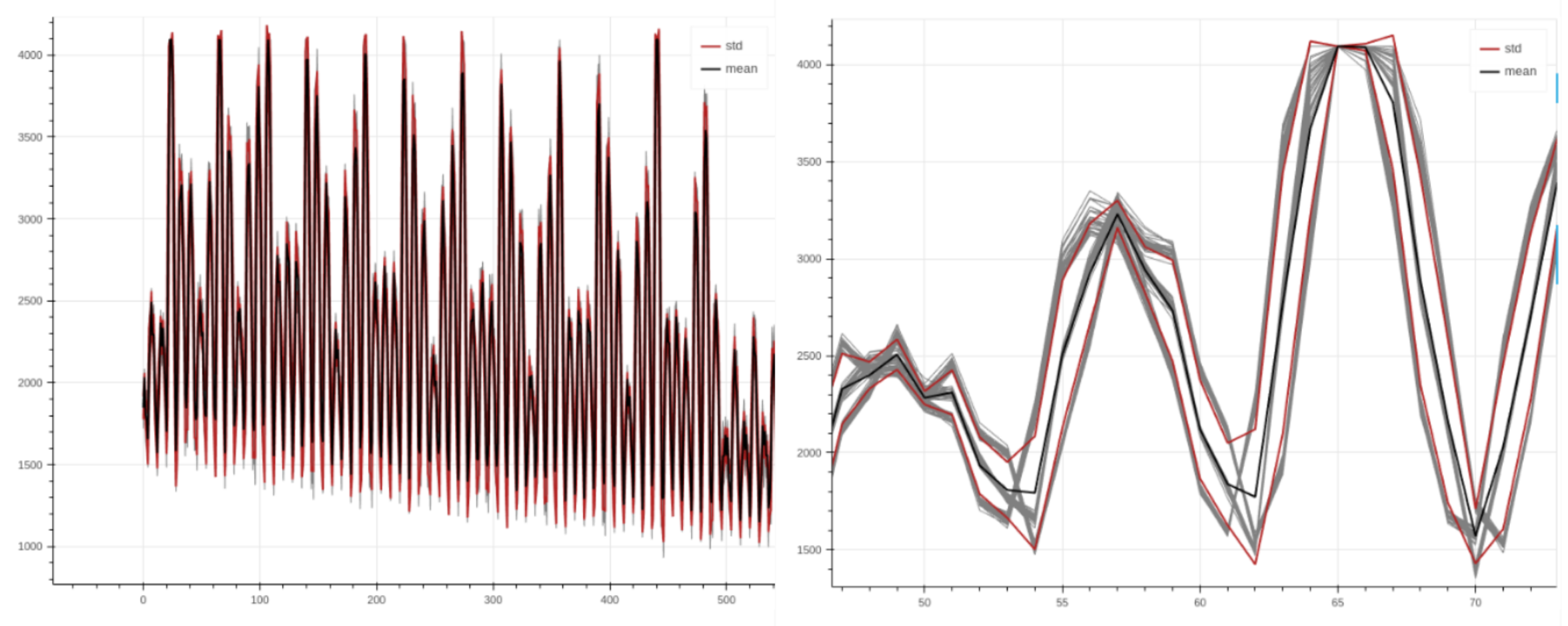 :--:
Figure 3: Power trace with AES encryption rounds visible (left). Aligned traces when zooming in (right).
:--:
Figure 3: Power trace with AES encryption rounds visible (left). Aligned traces when zooming in (right).
Figure 3 depicts power traces captured during AES-GCM encryptions with the setup above. As shown in the figure, the traces are nicely aligned, allowing to perform a sound evaluation.
Methodology
To detect whether the hardened GHASH implementation effectively mitigates SCA attacks, the Test Vector Leakage Assessment (TVLA) approach discussed by Rambus in a whitepaper is adapted for the GCM mode of AES. In TVLA, Welch’s t-test is used to determine whether it is possible to statistically distinguish two power trace sets from each other. This test returns a value t for each sample, where a value of |t| > 4.5 means that, with a high probability, a data dependent leakage was detected. However, note that this test cannot provide any information whether the leakage is actually exploitable.
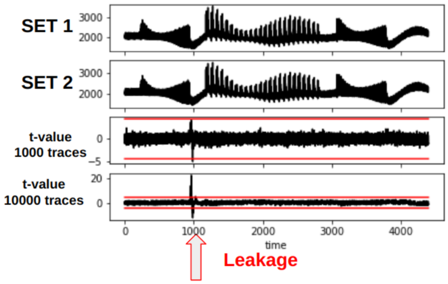 :--
Figure 4: TVLA plot showing leakage at around sample 1000. When increasing the number of traces (from 1000 to 10000), the leakage becomes more present. Note that the traces shown in this plot are taken from an arbitrary cryptographic hardware block and not AES.
:--
Figure 4: TVLA plot showing leakage at around sample 1000. When increasing the number of traces (from 1000 to 10000), the leakage becomes more present. Note that the traces shown in this plot are taken from an arbitrary cryptographic hardware block and not AES.
Figure 4 shows a TVLA plot that will be used throughout this document. The red lines mark the ± t-test border.
Dataset Generation for FvsR IV & Key
In TVLA, two different trace data sets need to be recorded. As described in the whitepaper, we generate these two trace data sets by using a fixed and a random AES-GCM cipher input set, i.e., the fixed and the random set.
| Input | Fixed Set | Random Set |
|---|---|---|
| Key | STATIC | RANDOM |
| IV | STATIC | RANDOM |
| PTX | STATIC | STATIC |
| AAD | STATIC | STATIC |
As shown in the table above, for our experiment we use a static cipher input for the fixed set. For the random set, we use a PRNG to randomly generate the secrets, i.e., key and IV, for each encryption. The dataset is generated directly on the device in the pentest framework. For each trace, ot-sca stores information to which dataset the trace belongs to.
With TVLA, the idea is to check whether we are able to distinguish power traces from the fixed and the random set.
Dataset Generation for FvsR PTX & AAD
For the second experiment, we use a static IV and key and calculate a FvsR PTX and AAD set:
| Input | Fixed Set | Random Set |
|---|---|---|
| Key | STATIC | STATIC |
| IV | STATIC | STATIC |
| PTX | STATIC | RANDOM |
| AAD | STATIC | RANDOM |
Results – FvsR IV & Key
In the following, we discuss the analysis results for each GCM phase. We start with the results for the FvsR IV & Key datasets.
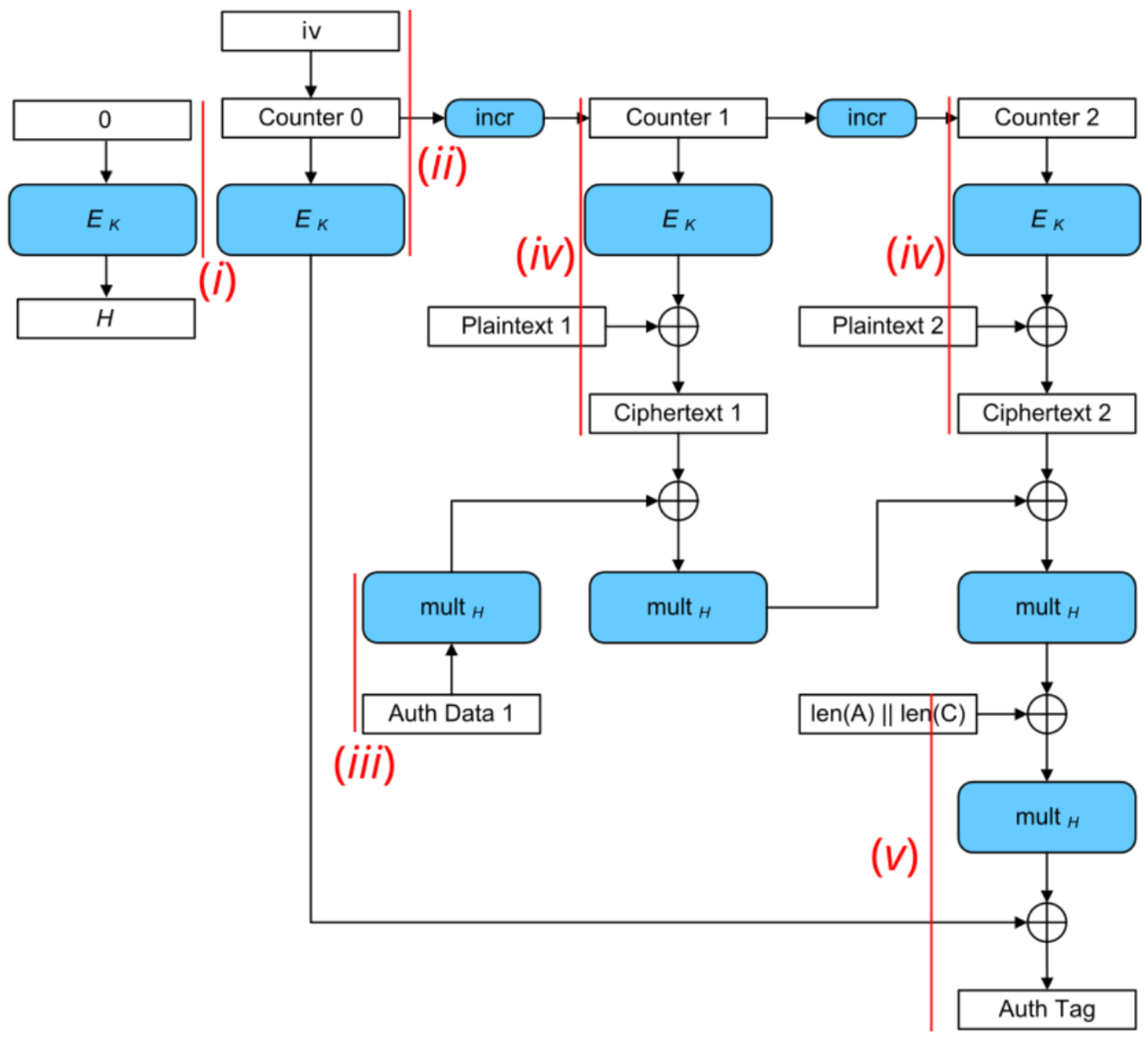 :--:
Figure 5: AES-GCM block diagram. Red lines mark the trigger windows for each analysis step.
:--:
Figure 5: AES-GCM block diagram. Red lines mark the trigger windows for each analysis step.
As shown in Figure 5, we focus on analyzing (i) the generation of the hash subkey H, (ii) the encryption of the initial counter block S, (iii) the processing of the AAD blocks, (iv) the plaintext blocks, and (v) the tag generation. Each measurement is conducted with (a) masks off and (b) masks on to analyze the effectiveness of the masking countermeasure.
i) SCA Evaluation of Generating the Hash Subkey H
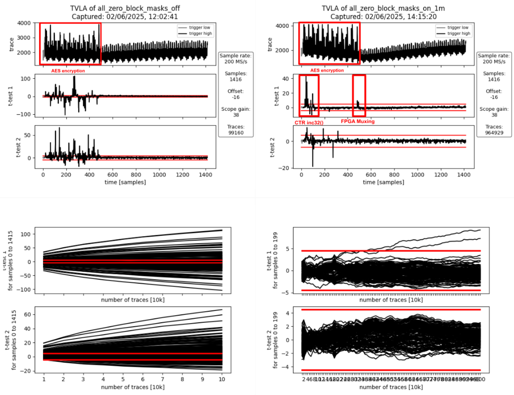 :--:
:--:
| Figure 6a: Masking Off - 100k traces - Figure 6b: Masking On - 1M traces |
Interpretation
The AES encryption is clearly visible in the form of 12 distinct peaks in the power traces shown Figures 6a and 6b. The 12 peaks correspond to first the loading of the key and the all-zero block into the AES cipher core, followed by the initial round and the 10 full AES rounds (AES-128). They spread over approximately 470 samples which corresponds to the 56 target clock cycles a full AES-128 encryption takes.
If the masking is turned off (Figure 6a), first and second-order leakage is clearly visible throughout the operation. If the masking is on (Figure 6b), there is first-order leakage 1) at the beginning as well as 2) at the end of the operation.
- The leakage at the beginning of the operation is due to incrementing the IV/CTR value (inc32 function in GCM spec) which spreads across the first two AES rounds. This produces first-order leakage as the inc32 function implementation isn’t masked. It doesn’t need to be masked as the IV is not secret, just the encrypted initial counter block S (i.e., the encrypted IV) is secret in the context of GCM.
- The leakage at the end of the operation happens when the masked output of the AES cipher core, i.e., the masked hash subkey H, gets loaded in shares into the GHASH block. When studying the RTL, one can see that there is nothing in the path between the AES cipher core and the hash subkey registers inside the GHASH block that could combine the shares and cause this leakage. The leakage is most likely due to how the FPGA implementation tool maps the flip flops of the hash subkey register shares to the available FPGA logic slices: if flip flops of the different shares get mapped to the same logic slice, the carry-chain and other muxing logic present in the logic slice can combine the various inputs thereby causing SCA leakage despite these logic outputs not being used. We’ve observed similar effects in the past and there is research giving more insight into this and other FPGA-specific issues.
To summarize, the observed first-order leakage if masking is on (Figure 6b) is not of concern for ASIC implementations.
ii) SCA Evaluation of Encrypting the Initial Counter Block
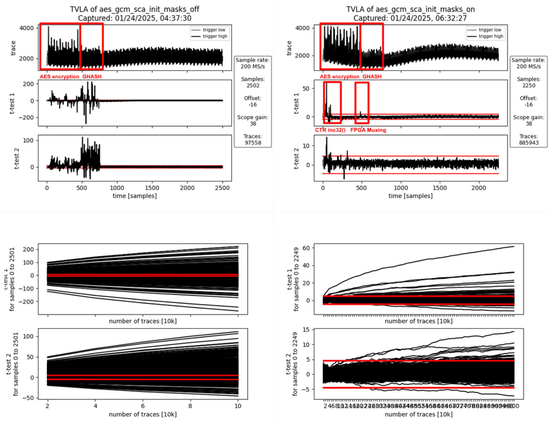 :--:
:--:
| Figure 7a: Masking Off - 100k traces - Figure 7b: Masking On - 1M traces |
Interpretation
Again, the AES encryption is clearly visible in the form of 12 peaks in the power traces shown Figures 7a and 7b. This AES encryption corresponds to the generation of the encrypted initial counter block S. The AES encryption is followed by another operation visible in the power trace: the computation of repeatedly used correction terms using the Galois-field multipliers inside GHASH. This operation takes 33 target clock cycles (approximately 275 samples).
If the masking is turned off (Figure 7a), first and second-order leakage is clearly visible throughout both operations while being more pronounced during the GHASH operation. This is because the GHASH block is smaller and thus produces less noise. If the masking is on (Figure 7b), there is first-order leakage 1) at the beginning as well as 2) between the two operations.
- As before, the leakage at the beginning of the operation is due to incrementing the IV/CTR value (inc32 function in GCM spec) which spreads across the first two AES rounds. This produces first-order leakage as the inc32 function implementation isn’t masked. It doesn’t need to be masked as the IV is not secret, just the encrypted initial counter block S (i.e., the encrypted IV) is secret in the context of GCM.
- As before, the leakage at the end of the operation happens when the masked output of the AES cipher core, i.e., the encrypted initial counter block gets loaded in shares into the GHASH block. When studying the RTL, one can see that there is nothing in the path between the AES cipher core and the GHASH state registers inside the GHASH block that could combine the shares and cause this leakage. As before, the leakage is most likely due to how the FPGA implementation tool maps the multiplexers in front of the GHASH state registers to the available FPGA logic slices: Since the multiplexers for both shares use the same control signals, the multiplexing logic can be combined even into the same look-up tables (LUTs) thereby causing SCA leakage. We’ve observed similar effects in the past and there is research giving more insight into this and other FPGA-specific issues.
To summarize, the observed first-order leakage if masking is on (FIgure 7b) is not of concern for ASIC implementations.
iii) SCA Evaluation of Processing the AAD Blocks
Processing AAD Block 0
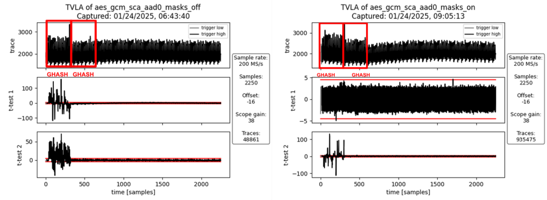 :--:
:--:
| Figure 8a: Masking Off - 50k traces - Figure 8b: Masking On - 10M traces |
Interpretation
For AAD blocks, the AES cipher core is not involved. However, during the computation of the first AAD block, the GHASH block needs to compute an additional correction term which is used for the very first block only. If the masking is turned off (Figure 8a), first- and second-order leakage is clearly visible but only for the first activity block. The second activity block involves computing the additional correction terms which requires Share 1 of the encrypted initial counter block to be multiplied by Share 1 of the hash subkey. But since the masking is off, both these values are zero for both the fixed and the random set and hence there is no SCA leakage. If the masking is turned on (Figure 8b), no SCA leakage is observable which is desirable.
Processing AAD Block 1
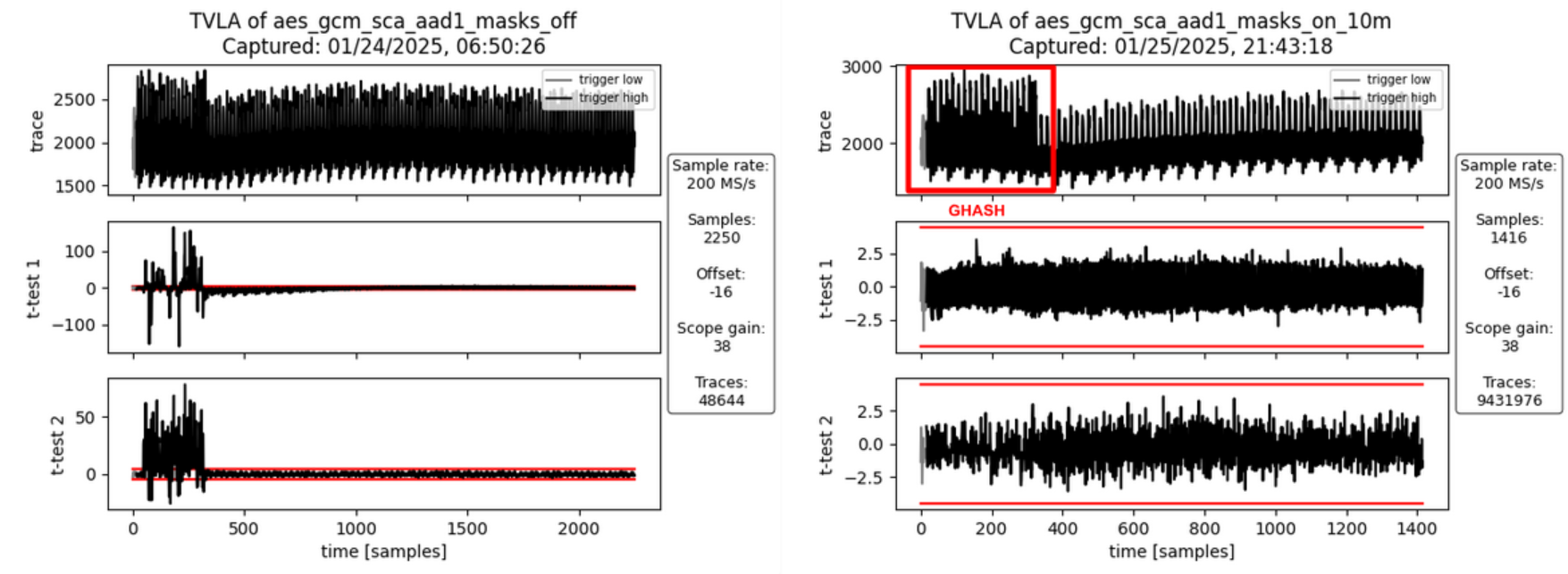 :--:
:--:
| Figure 9a: Masking Off - 50k traces - Figure 9b: Masking On - 10M traces |
Interpretation
For the second AAD block (and any subsequent AAD blocks) there is only one activity block corresponding to the Galois-field multiplication. If masking is turned off (Figure 9a), there is both first- and second-order leakage observable. If the masking is turned on (Figure 9b), no SCA leakage is observable which is desirable.
iv) SCA Evaluation of Processing the PTX Blocks
Processing PTX Block 0
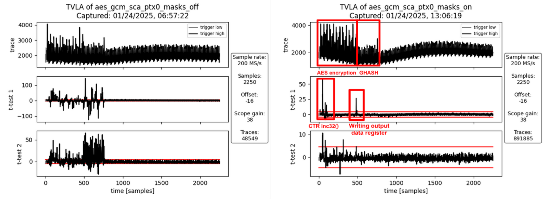 :--:
:--:
| Figure 10a: Masking Off - 50k traces - Figure 10b: Masking On - 1M traces |
Interpretation
Like in ii) SCA Evaluation of Encrypting the Initial Counter Block there is first-order leakage 1) at the beginning and 2) between the two operations if the masking is turned on (Figure 10b).
- As before, the leakage at the beginning of the operation is due to incrementing the IV/CTR value (inc32 function in GCM spec) which spreads across the first two AES rounds. This produces first-order leakage as the inc32 function implementation isn’t masked. It doesn’t need to be masked as the IV is not secret, just the encrypted initial counter block S (i.e., the encrypted IV) is secret in the context of GCM.
- The leakage between the two operations is due to the unmasking of the AES cipher core output, the addition of input data to produce the ciphertext, and writing this value to the GHASH block and the output data registers. It’s not related to the hash subkey H or the initial counter block S (i.e. the two secrets involved in the GHASH part of GCM). But since the AAD and the plaintext have been chosen to be the same for all traces in the fixed and the random sets, the traces of the fixed set only produce all the same ciphertext and thus are expected to exhibit a static power signature for this step, whereas the ciphertext of the random set is randomized through the random key and IV. However, since the ciphertext is not secret in the context of GCM, this leakage is of no concern.
To summarize, the observed first-order leakage if masking is on (FIgure 10b) is not of concern.
Processing PTX Block 1
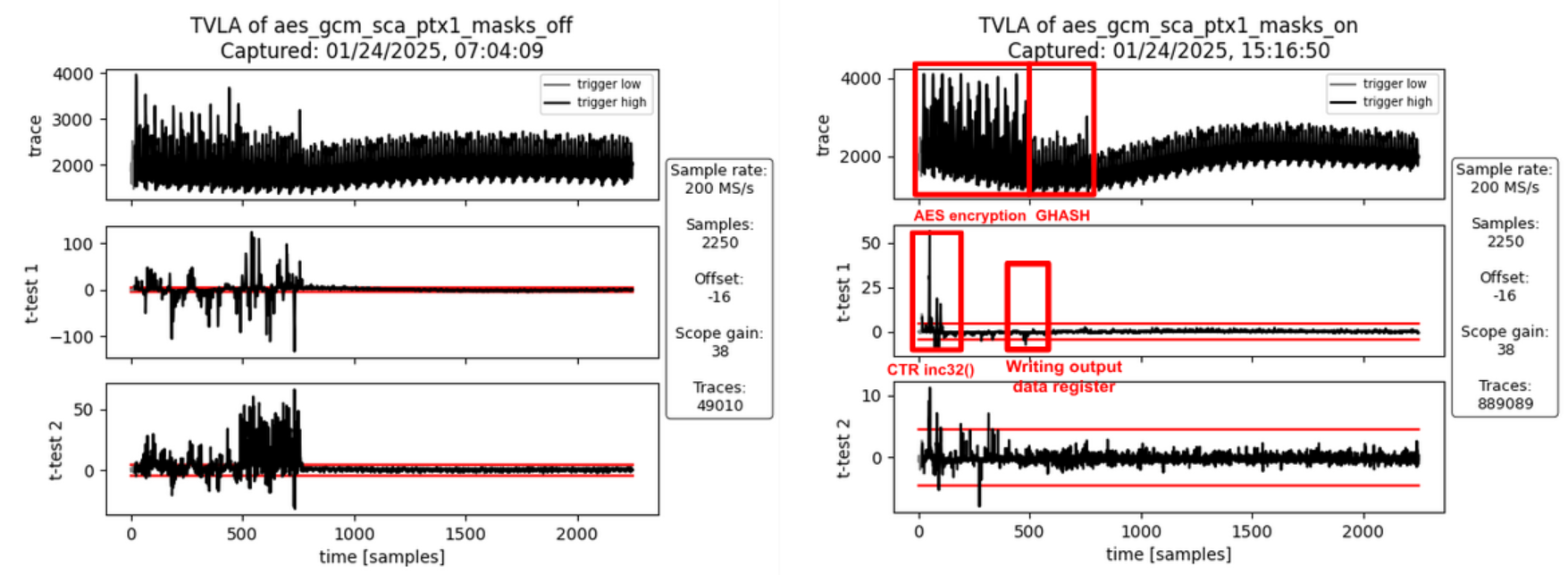 :--:
:--:
| Figure 11a: Masking Off - 50k traces - Figure 11b: Masking On - 1M traces |
Interpretation
As before (PTX Block 0), there is some first-order leakage observable when the masking is turned on. For the same reasons as before, this leakage is not of concern.
v) SCA Evaluation of the Tag Generation
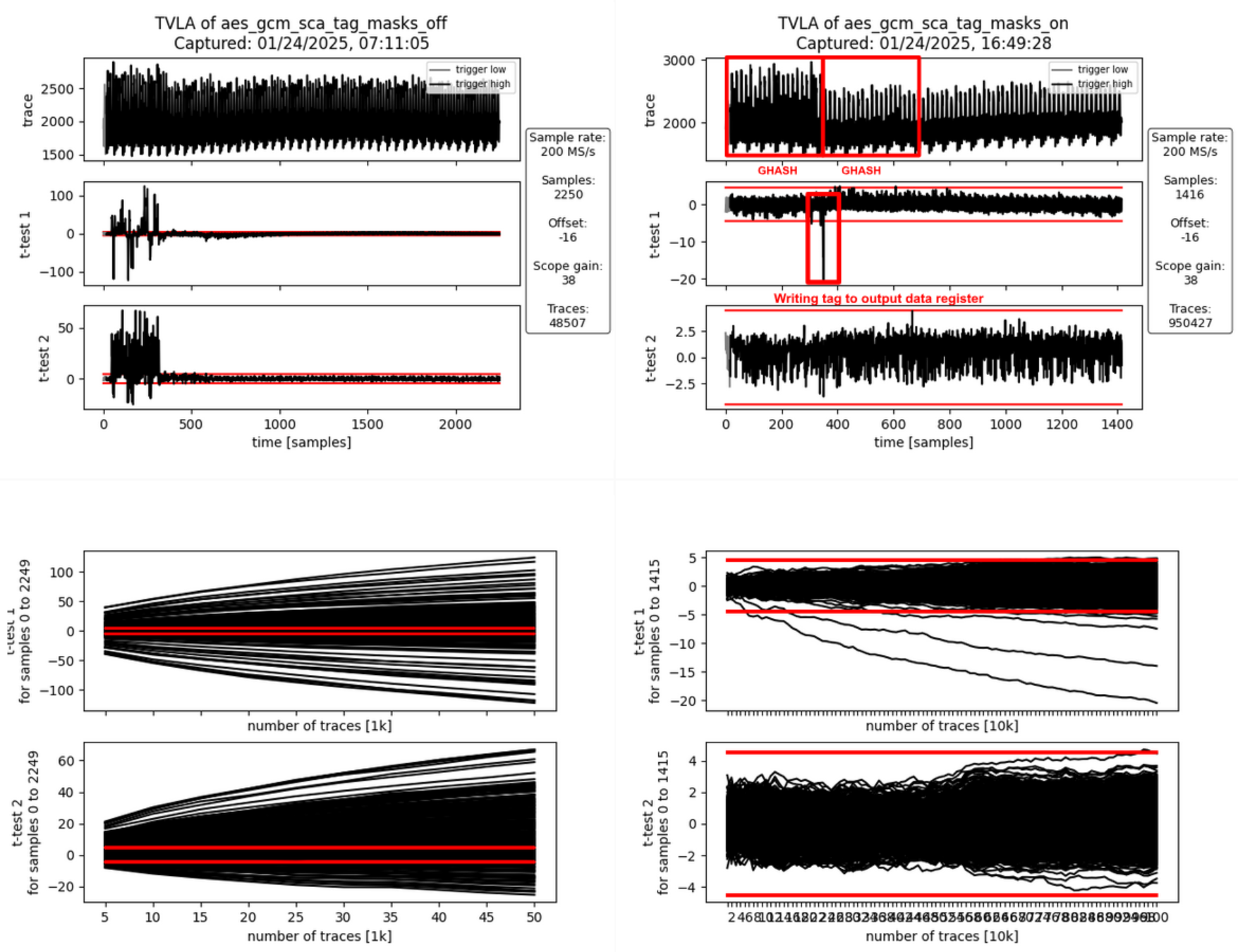 :--:
:--:
| Figure 12a: Masking Off - 50k traces - Figure 12b: Masking On - 1M traces |
Interpretation
The generation of the final authentication tag consists of two operations.
- The 128-bit block containing the AAD and ciphertext lengths is hashed and the correction terms are added. The GHASH state is unmasked (still masked with the encrypted initial counter block S) and Share 1 of S is added to write the final authentication tag to the data output registers readable by software.
- In parallel to writing the final authentication tag to the data output registers, the internal state is all cleared to random values and an additional multiplication is triggered to clear the internal state of the Galois-field multipliers and the correction term registers.
If masking is turned off (Figure 12a), there is both first- and second-order leakage observable during the first activity block (tag generation) but not during the clearing operation. If the masking is turned on (Figure 12b), some SCA leakage is observable between the two operations, i.e., when the final authentication tag is written to the output data registers. This leakage is expected as both the fixed and the random data sets use a static AAD and plaintext. This means, the tag for the fixed data set is fixed whereas the tags for the random set get randomized through the ciphertext (random due to the random key and IV).
To summarize, the observed first-order leakage if masking is on (FIgure 12b) is not of concern.
Results – FvsR PTX & AAD
In the following, we discuss the analysis results for each FvsR PTX & AAD datasets. These experiments were specifically done to investigate leakage peaks identified for the FvsR Key & IV datasets that are attributed to how the FPGA implementation tool maps flip flops and multiplexer shares to the available FPGA logic slices.
i) SCA Evaluation of Generating the Hash Subkey H
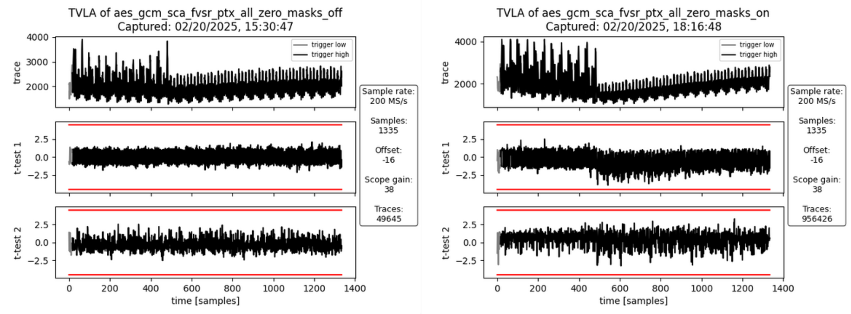 :--:
:--:
| Figure 13a: Masking Off - 50k traces - Figure 13b: Masking On - 1M traces |
Interpretation
There is no SCA leakage visible in both cases without masking (Figure 13a) and with masking turned on (Figure 13b). This is expected as the hash subkey generation doesn’t involve the plaintext and the AAD but only the key and IV. Both the fixed and random set use the same static key and IV.
This experiment was specifically done to check whether the leakage identified in Figure 6b and attributed to how the FPGA implementation tool maps the flip flops of the hash subkey register shares to the available FPGA logic slices. As expected, the leakage peak is now gone.
ii) SCA Evaluation of Encrypting the Initial Counter Block
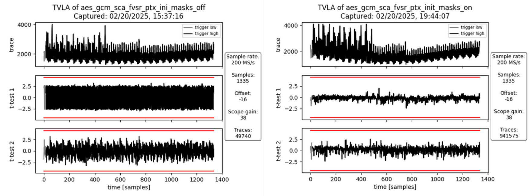 :--:
:--:
| Figure 14a: Masking Off - 50k traces - Figure 14b: Masking On - 1M traces |
Interpretation
There is no SCA leakage visible in both cases without masking (Figure 14a) and with masking turned on (Figure 14b). This is expected as the encryption of the initial counter block and the subsequent computation of repeatedly used correction terms doesn’t involve the plaintext and the AAD but only the key and IV. Both the fixed and random set use the same static key and IV.
This experiment was specifically done to check whether the leakage identified in Figure 7b and attributed to how the FPGA implementation tool maps the multiplexers in front of the GHASH state registers to the available FPGA logic slices. As expected, the leakage peak is now gone.
iv) SCA Evaluation of Processing the PTX Block 0
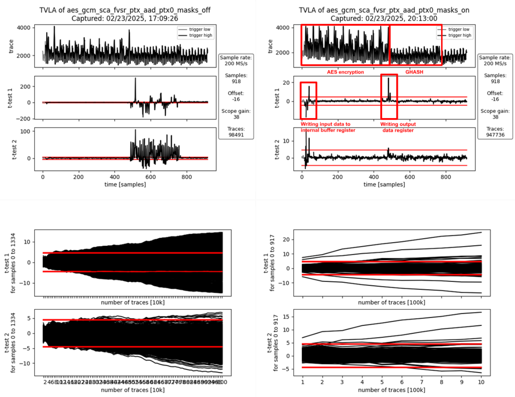 :--:
:--:
| Figure 15a: Masking Off - 100k traces - Figure 15b: Masking On - 1M traces |
Interpretation
With the masking turned off (Figure 15a), there is first-order leakage 1) at the beginning of the operation and 2) throughout the entire GHASH operation.
- The leakage at the beginning of the operation is due to the input data (the plaintext) being written to an internal buffer register. The AES cipher is operated in counter mode, meaning it doesn’t encrypt the input data but the counter value (incremented IV). Because the IV is fixed for both the fixed and the random data set, no leakage is observed during the AES encryption even if the masking is off. At the end of the AES encryption, the output of the AES cipher core is added to the content of the buffer register to produce the ciphertext which is then forwarded to the GHASH block and to the data output registers.
- The GHASH operation then processes this ciphertext. The observed leakage when the masking is off is expected.
With the masking turned on (Figure 15b), the first-order leakage at the beginning of the operation remains visible. The reason for this is that the internal register buffering the previous input data is not masked. This is of no concern as the leakage is not related to key or IV.
Another first-order leakage peak is visible between the AES encryption and the GHASH operation. This leakage is due to the unmasked AES cipher core output being added to the input data (coming from the internal buffer register) and the result being stored to the output data register. As key and IV are static and identical for both the fixed and the random data set, the cipher core output is the same for both sets. Any difference in the power signature between the two sets is due to the different plaintext / ciphertext. Again, this is to be expected and of no concern as the ciphertext is not secret in the context of GCM.
Reproducing the FPGA Experiments
Prerequisites
(i) Setting up the CW310 and CW Husky
Please follow the guide here to prepare the CW310 and CW Husky for the SCA measurements.
(ii) Generating the FPGA Bitstream
Follow the guide here to install Xilinx Vivado. Please note that a valid license is needed to generate bitstreams for the CW310 FPGA board.
Then, build the bitstream from the aes-gcm-sca-bitstream branch. This branch includes the AES-GCM and applies several optimizations (disabling certain features to reduce the area utilization) to improve the SCA measurements.
git clone https://github.com/vogelpi/opentitan.git
cd opentitan
git checkout aes-gcm-sca-bitstream
./bazelisk.sh build //hw/bitstream/vivado:fpga_cw310_test_rom
cp bazel-bin/hw/bitstream/vivado/build.fpga_cw310/synth-vivado/lowrisc_systems_chip_earlgrey_cw310_0.1.bit .
The resulting bitstream is lowrisc_systems_chip_earlgrey_cw310_0.1.bit.
(iii) Compiling the Penetration Testing Binary
The penetration testing binary that is running on the target is the framework that receives commands from the side-channel evaluation framework and triggers the AES-GCM operations.
git clone <https://github.com/vogelpi/opentitan.git>
cd opentitan
git checkout aes-gcm-review
./bazelisk.sh build //sw/device/tests/penetrationtests/firmware:firmware_fpga_cw310_test_rom
cp bazel-bin/sw/device/tests/penetrationtests/firmware/firmware_fpga_cw310_test_rom_fpga_cw310_test_rom.bin sca_ujson_fpga_cw310.bin
The resulting penetration testing binary is sca_ujson_fpga_cw310.bin.
(iv) Setting up the Side-Channel Evaluation Framework
Clone the ot-sca repository and switch to the dedicated AES-GCM branch:
git clone <https://github.com/lowRISC/ot-sca.git>
cd ot-sca
git checkout ot-sca-aes-gcm
Then, follow this guideline to prepare your machine for the measurements.
Afterwards, copy the bitstream to ot-sca/objs/lowrisc_systems_chip_earlgrey_cw310_0.1.bit and the binary to ot-sca/objs/sca_ujson_fpga_cw310.bin.
Finally, determine the port the CW310 opened on your machine (e.g., /dev/ttyACM2) and set it accordingly in the port field of the ot-sca/capture/configs/aes_gcm_sca_cw310.yaml configuration file.
Capturing Traces
After fulfilling the prerequisites, traces can be captured using ot-sca.
To configure the measurement, adapt the script located in ot-sca/capture/configs/aes_gcm_sca_cw310.yaml.
The following parameters can be changed:
husky:
  # Number of encryptions performed in one batch.
  num_segments: 35
  # Number of cycles that are captured by the CW Husky.
  num_cycles: 320
capture:
  # Number of traces to capture.
  num_traces: 100000
  # Number of traces to keep in memory before flushing to the disk.
  trace_threshold: 50000
test:
  # Values used for the fixed set.
  iv_fixed: [0xDE, 0xAD, 0xBE, 0xEF, 0xCA, 0xFE, 0xBA, 0xAD, 0xF0, 0xCA,
             0xCC, 0x1A, 0x00, 0x00, 0x00, 0x00]
  key_fixed: [0x81, 0x1E, 0x37, 0x31, 0xB0, 0x12, 0x0A, 0x78, 0x42, 0x78,
              0x1E, 0x22, 0xB2, 0x5C, 0xDD, 0xF9]
  # Static values that are used by the fixed and the random set.
  ptx_blocks: 2
  ptx_static: [[0xAA, 0xAA, 0xAA, 0xAA, 0xAA, 0xAA, 0xAA, 0xAA, 0xAA, 0xAA,
                0xAA, 0xAA, 0xAA, 0xAA, 0xAA, 0xAA], [0xBB, 0xBB, 0xBB,
                0xBB, 0xBB, 0xBB, 0xBB, 0xBB, 0xBB, 0xBB, 0xBB, 0xBB, 0xBB,
                0xBB, 0xBB, 0xBB]]
  ptx_last_block_len_bytes: 16
  aad_blocks: 2
  aad_static: [[0xCC, 0xCC, 0xCC, 0xCC, 0xCC, 0xCC, 0xCC, 0xCC, 0xCC, 0xCC,
                 0xCC, 0xCC, 0xCC, 0xCC, 0xCC, 0xCC], [0xDD, 0xDD, 0xDD,
                 0xDD, 0xDD, 0xDD, 0xDD, 0xDD, 0xDD, 0xDD, 0xDD, 0xDD,
                 0xDD, 0xDD, 0xDD, 0xDD]]
  aad_last_block_len_bytes: 16
  # Trigger configuration (select only one).
  # [Hash sub key, Init. block, AAD block, PTX block, TAG block]
  triggers: [False, False, False, False, True]
  # Which AAD or PTX block.  0 = first block.
  trigger_block: 0
  # 32-bit seed for masking on device. To switch off the masking, use 0
  # as an LFSR seed.
  lfsr_seed: 0x00000000
  #lfsr_seed: 0xdeadbeef
After tweaking the configuration, the traces can be captured by executing:
cd capture
./capture_aes_gcm.py -c configs/aes_gcm_sca_cw310.yaml -p aes_gcm_sca
Where the -c parameter is the config and -p the database where the traces are stored.
Performing the TVLA
After capturing the traces, the TVLA can be performed by switching into the ot-sca/analysis folder, copying the ot-sca/analysis/configs/tvla_cfg_kmac.yaml file to ot-sca/analysis/configs/tvla_cfg_aes_gcm.yaml, and modifying the configuration file:
project_file: ../capture/projects/aes_gcm_sca
trace_file: null
trace_start: null
trace_end: null
leakage_file: null
save_to_disk: null
save_to_disk_ttest: null
round_select: null
byte_select: null
input_histogram_file: null
output_histogram_file: null
number_of_steps: 1
ttest_step_file: null
plot_figures: true
test_type: "GENERAL_KEY"
mode: aes
filter_traces: true
trace_threshold: 50000
trace_db: ot_trace_library
By calling
./tvla.py --cfg-file tvla_cfg_aes_gcm.yaml run-tvla
the TVLA plot is generated.
PCR vault
- Platform Configuration Register (PCR) vault is a register file that stores measurements to be used by the microcontroller.
- PCR entries are read-only registers of 512 bits each.
- Control bits allow for entries to be cleared by FW, which sets their values back to 0.
- A lock bit can be set by FW to prevent the entry from being cleared. The lock bit is sticky and only resets on a powergood cycle.
| PCRV register | Address Offset | Description |
|---|---|---|
| PCR Control[31:0] | 0x1001a000 | 32 Control registers, 32 bits each |
| PCR Entry[31:0][11:0][31:0] | 0x1001a600 | 32 PCR entries, 384 bits each |
PCR vault functional block
PCR entries are hash extended using a hash extension function. The hash extension function takes the data currently in the PCR entry specified, concatenates data provided by the FW, and performs a SHA384 function on that data, storing the result back into the same PCR entry.
PCR hash extend function
FW provides the PCR entry to use as source and destination of the hash extend. HW copies the PCR into the start of the SHA block and locks those dwords from FW access. FW then provides the new data, and runs the SHA function as usual. After initialization, the locked dwords are unlocked.
FW must set a last cycle flag before running the last iteration of the SHA engine. This could be the first “init” cycle, or the Nth “next” cycle. This flag allows HW to copy the final resulting hash output back to the source PCR.
PCR signing
- PCR signing uses the key in key slot index 7 for PCR signing
- HW implements a HW function called GEN_PCR_HASH
- HW reads all the PCRs from all the PCR slots and hash extends them along with the NONCE that Caliptra FW provides
- PCR Hash = Hash(PCR[0], …, PCR[31], Nonce)
- HW also implements a HW function called SIGN_PCR. This function takes the PCR digest that was generated by the previous routine and signs it using the key in key slot 7, following the same ECC sign flow defined in the ECC section.
- The resulting PCR DIGEST is used only once for signing by the HW. If a new PCR signing is required, GEN_PCR_HASH needs to be redone.
Key vault
Key Vault (KV) is a register file that stores the keys to be used by the microcontroller, but this register file is not observed by the microcontroller. Each cryptographic function has a control register and functional block designed to read from and write to the KV.
| KV register | Description |
|---|---|
| Key Control[23:0] | 24 Control registers, 32 bits each |
| Key Entry[23:0][15:0][31:0] | 24 Key entries, 512 bits each No read or write access |
Key vault functional block
Keys and measurements are stored in 512b register files. These have no read or write path from the microcontroller. The entries are read through a passive read mux driven by each cryptographic block. Locked entries return zeroes.
Entries in the KV must be cleared via control register, or by de-assertion of pwrgood.
Each entry has a control register that is writable by the microcontroller.
The destination valid field is programmed by FW in the cryptographic block generating the key, and it is passed here at generation time. This field cannot be modified after the key is generated and stored in the KV.
| KV Entry Ctrl Fields | Reset | Description |
|---|---|---|
| Lock wr[0] | core_only_rst_b | Setting the lock wr field prevents the entry from being written by the microcontroller. Keys are always locked. After a lock is set, it cannot be reset until cptra_rst_b is de-asserted. |
| Lock use[1] | core_only_rst_b | Setting the lock use field prevents the entry from being used in any cryptographic blocks. After the lock is set, it cannot be reset until cptra_rst_b is de-asserted. |
| Clear[2] | cptra_rst_b | If unlocked, setting the clear bit causes KV to clear the associated entry. The clear bit is reset after entry is cleared. |
| Copy[3] | cptra_rst_b | ENHANCEMENT: Setting the copy bit causes KV to copy the key to the entry written to Copy Dest field. |
| Copy Dest[8:4] | cptra_rst_b | ENHANCEMENT: Destination entry for the copy function. |
| Dest_valid[16:9] | hard_reset_b | KV entry can be used with the associated cryptographic block if the appropriate index is set. [0] - HMAC KEY [1] - HMAC BLOCK [2] - MLDSA SEED [3] - ECC PRIVKEY [4] - ECC SEED [5] - AES KEY [7:6] - RSVD |
| last_dword[20:19] | hard_reset_b | Store the offset of the last valid dword, used to indicate the last cycle for read operations. |
Key vault cryptographic functional block
A generic block is instantiated in each cryptographic block to enable access to KV.
Each input to a cryptographic engine can have a key vault read block associated with it. The KV read block takes in a key vault read control register that drives an FSM to copy an entry from the key vault into the appropriate input register of the cryptographic engine.
Each output generated by a cryptographic engine can have its result copied to a slot in the key vault. The KV write block takes in a key vault write control register. This register drives an FSM to copy the result from the cryptographic engine into the appropriate key vault entry. It also programs a control field for that entry to indicate where that entry can be used.
After programming the key vault read control, FW needs to query the associated key vault read status to confirm that the requested key was copied successfully. After valid is set and the error field reports success, the key is ready to be used.
Similarly, after programming the key vault write control and initiating the cryptographic function that generates the key to be written, FW needs to query the associated key vault write status to confirm that the requested key was generated and written successfully.
When a key is read from the key vault, the API register is locked and any result generated from the cryptographic block is not readable by firmware. The digest can only be sent to the key vault by appropriately programming the key vault write controls. After the cryptographic block completes its operation, the lock is cleared and the key is cleared from the API registers.
If multiple iterations of the cryptographic function are required, the key vault read and write controls must be programmed for each iteration. This ensures that the lock is set and the digest is not readable.
The following tables describe read, write, and status values for key vault blocks.
| KV Read Ctrl Reg | Description |
|---|---|
| read_en[0] | Indicates that the read data is to come from the key vault. Setting this bit to 1 initiates copying of data from the key vault. |
| read_entry[5:1] | Key vault entry to retrieve the read data from the engine. |
| pcr_hash_extend[6] | Requested entry is a PCR. This is used only for the SHA engine to hash extend. It is not functional in any other cryptographic engine. |
| rsvd[31:7] | Reserved field |
| KV Write Ctrl Reg | Description |
|---|---|
| write_en[0] | Indicates that the result is to be stored in the key vault. Setting this bit to 1 copies the result to the key vault when it is ready. |
| write_entry[5:1] | Key vault entry to store the result. |
| hmac_key_dest_valid[6] | HMAC KEY is a valid destination. |
| hmac_block_dest_valid[7] | HMAC BLOCK is a valid destination. |
| mldsa_seed_dest_valid[8] | MLDSA SEED is a valid destination. |
| ecc_pkey_dest_valid[9] | ECC PKEY is a valid destination. |
| ecc_seed_dest_valid[10] | ECC SEED is a valid destination. |
| aes_key_dest_valid[11] | AES KEY is a valid destination. |
| rsvd[31:12] | Reserved field |
| KV Status Reg | Description |
|---|---|
| ready[0] | Key vault control is idle and ready for a command. |
| valid[1] | Requested flow is done. |
| error[9:2] | SUCCESS - 0x0 - Key Vault flow was successful KV_READ_FAIL - 0x1 - Key Vault Read flow failed KV_WRITE_FAIL - 0x2 - Key Vault Write flow failed |
De-obfuscation engine
To protect software intellectual property from different attacks and, particularly, for thwarting an array of supply chain threats, code obfuscation is employed. Hence, the de-obfuscation engine is implemented to decrypt the code.
Advanced Encryption Standard (AES) is used as a de-obfuscation function to encrypt and decrypt data [4]. The hardware implementation is based on Secworks/aes [1]. The implementation supports the two variants: 128- and 256-bit keys with a block/chunk size of 128 bits.
The AES algorithm is described as follows:
- The key is fed to an AES core to compute and initialize the round key
- The message is broken into 128-bit chunks by the host
- For each chunk:
- The message is fed to the AES core
- The AES core and its working mode (enc/dec) are triggered by the host
- The AES core status is changed to ready after encryption or decryption processing
- The result digest can be read before processing the next message chunks
Key vault de-obfuscation block operation
A de-obfuscation engine (DOE) is used in conjunction with AES cryptography to de-obfuscate the UDS and field entropy.
- The obfuscation key is driven to the AES key. The data to be decrypted (either obfuscated UDS or obfuscated field entropy) is fed into the AES data.
- An FSM manually drives the AES engine and writes the decrypted data back to the key vault.
- FW programs the DOE with the requested function (UDS or field entropy de-obfuscation), and the destination for the result.
- After de-obfuscation is complete, FW can clear out the UDS and field entropy values from any flops until cptra_pwrgood de-assertion.
The following tables describe DOE register and control fields.
| DOE Register | Address | Description |
|---|---|---|
| IV | 0x10000000 | 128 bit IV for DOE flow. Stored in big-endian representation. |
| CTRL | 0x10000010 | Controls for DOE flows. |
| STATUS | 0x10000014 | Valid indicates the command is done and results are stored in key vault. Ready indicates the core is ready for another command. |
| DOE Ctrl Fields | Reset | Description |
|---|---|---|
| COMMAND[1:0] | Cptra_rst_b | 2’b00 Idle 2’b01 Run UDS flow 2’b10 Run FE flow 2’b11 Clear Obf Secrets |
| DEST[4:2] | Cptra_rst_b | Destination register for the result of the de-obfuscation flow. Field entropy writes into DEST and DEST+1 Key entry only, can’t go to PCR . |
Key vault de-obfuscation flow
- ROM loads IV into DOE. ROM writes to the DOE control register the destination for the de-obfuscated result and sets the appropriate bit to run UDS and/or the field entropy flow.
- DOE state machine takes over and loads the Caliptra obfuscation key into the key register.
- Next, either the obfuscated UDS or field entropy are loaded into the block register 4 DWORDS at a time.
- Results are written to the KV entry specified in the DEST field of the DOE control register.
- State machine resets the appropriate RUN bit when the de-obfuscated key is written to KV. FW can poll this register to know when the flow is complete.
- The clear obf secrets command flushes the obfuscation key, the obfuscated UDS, and the field entropy from the internal flops. This should be done by ROM after both de-obfuscation flows are complete.
Data vault
Data vault is a set of generic scratch pad registers with specific lock functionality and clearable on cold and warm resets.
- 48B scratchpad registers that are lockable but cleared on cold reset (10 registers)
- 48B scratchpad registers that are lockable but cleared on warm reset (10 registers)
- 4B scratchpad registers that are lockable but cleared on cold reset (8 registers)
- 4B scratchpad registers that are lockable but cleared on warm reset (10 registers)
- 4B scratchpad registers that are cleared on warm reset (8 registers)
Cryptographic blocks fatal and non-fatal errors
The following table describes cryptographic errors.
| Errors | Error type | Description |
|---|---|---|
| ECC_R_ZERO | HW_ERROR_NON_FATAL | Indicates a non-fatal error in ECC signing if the computed signature R is equal to 0. FW should change the message or privkey to perform a valid signing. |
| CRYPTO_ERROR | HW_ERROR_FATAL | Indicates a fatal error due to multiple cryptographic operations occurring simultaneously. FW must only operate one cryptographic engine at a time. |
Terminology
The following terminology is used in this document.
| Abbreviation | Description |
|---|---|
| AES | Advanced Encryption Standard |
| BMC | Baseboard Management Controller |
| CA | Certificate Authority |
| CDI | Composite Device Identifier |
| CPU | Central Processing Unit |
| CRL | Certificate Revocation List |
| CSR | Certificate Signing Request |
| CSP | Critical Security Parameter |
| DICE | Device Identifier Composition Engine |
| DME | Device Manufacturer Endorsement |
| DPA | Differential Power Analysis |
| DRBG | Deterministic Random Bit Generator |
| DWORD | 32-bit (4-byte) data element |
| ECDSA | Elliptic Curve Digital Signature Algorithm |
| ECDH | Elliptic Curve Deffie-Hellman Key Exchange |
| FMC | FW First Mutable Code |
| FSM | Finite State Machine |
| GPU | Graphics Processing Unit |
| HMAC | Hash-based message authentication code |
| IDevId | Initial Device Identifier |
| iRoT | Internal RoT |
| IV | Initial Vector |
| KAT | Known Answer Test |
| KDF | Key Derivation Function |
| LDevId | Locally Significant Device Identifier |
| MCTP | Management Component Transport Protocol |
| NIC | Network Interface Card |
| NIST | National Institute of Standards and technology |
| OCP | Open Compute Project |
| OTP | One-time programmable |
| PCR | Platform Configuration Register |
| PKI | Public Key infrastructure |
| PUF | Physically unclonable function |
| RNG | Random Number Generator |
| RoT | Root of Trust |
| RTI | RoT for Identity |
| RTM | RoT for Measurement |
| RTR | RoT for Reporting |
| SCA | Side-Channel Analysis |
| SHA | Secure Hash Algorithm |
| SoC | System on Chip |
| SPA | Simple Power Analysis |
| SPDM | Security Protocol and Data Model |
| SSD | Solid State Drive |
| TCB | Trusted Computing Base |
| TCI | TCB Component Identifier |
| TCG | Trusted Computing Group |
| TEE | Trusted Execution Environment |
| TRNG | True Random Number Generator |
| UECC | Uncorrectable Error Correction Code |
References
- J. Strömbergson, "Secworks," [Online]. Available at https://github.com/secworks.
- NIST, Federal Information Processing Standards Publication (FIPS PUB) 180-4 Secure Hash Standard (SHS).
- OpenSSL [Online]. Available at https://www.openssl.org/docs/man3.0/man3/SHA512.html.
- N. W. Group, RFC 3394, Advanced Encryption Standard (AES) Key Wrap Algorithm, 2002.
- NIST, Federal Information Processing Standards Publication (FIPS) 198-1, The Keyed-Hash Message Authentication Code, 2008.
- N. W. Group, RFC 4868, Using HMAC-SHA256, HMAC-SHA384, and HMAC-SHA512 with IPsec, 2007.
- RFC 6979, Deterministic Usage of the Digital Signature Algorithm (DSA) and Elliptic Curve Digital Signature Algorithm (ECDSA), 2013.
- TCG, Hardware Requirements for a Device Identifier Composition Engine, 2018.
- Coron, J.-S.: Resistance against differential power analysis for elliptic curve cryptosystems. In: Ko¸c, C¸ .K., Paar, C. (eds.) CHES 1999. LNCS, vol. 1717, pp. 292–302.
- Schindler, W., Wiemers, A.: Efficient side-channel attacks on scalar blinding on elliptic curves with special structure. In: NISTWorkshop on ECC Standards (2015).
- National Institute of Standards and Technology, "Digital Signature Standard (DSS)", Federal Information Processing Standards Publication (FIPS PUB) 186-4, July 2013.
- NIST SP 800-90A, Rev 1: "Recommendation for Random Number Generation Using Deterministic Random Bit Generators", 2012. |
- CHIPS Alliance, “RISC-V VeeR EL2 Programmer’s Reference Manual” [Online] Available at https://github.com/chipsalliance/Cores-VeeR-EL2/blob/main/docs/RISC-V_VeeR_EL2_PRM.pdf.
- “The RISC-V Instruction Set Manual, Volume I: User-Level ISA, Document Version 20191213”, Editors Andrew Waterman and Krste Asanovi ́c, RISC-V Foundation, December 2019. Available at https://riscv.org/technical/specifications/.
- “The RISC-V Instruction Set Manual, Volume II: Privileged Architecture, Document Version 20211203”, Editors Andrew Waterman, Krste Asanovi ́c, and John Hauser, RISC-V International, December 2021. Available at https://riscv.org/technical/specifications/.
- NIST SP 800-56A, Rev 3: "Recommendation for Pair-Wise Key-Establishment Schemes Using Discrete Logarithm Cryptography", 2018, |
[1] Caliptra.** **Spanish for “root cap” and describes the deepest part of the root