v2.0: Caliptra_boot_fsm.png
Image not present in this version
v2.1: Caliptra_boot_fsm.png
| @@ -1,12 +1,12 @@ | |||
| 1 | 1 | <div style="font-size: 0.85em; color: #656d76; margin-bottom: 1em; padding: 0.5em; background: #f6f8fa; border-radius: 4px;"> | |
| 2 | -📄 Source: <a href="https://github.com/chipsalliance/caliptra-rtl/blob/35b0bc5691b2bd0fc180403914cfabe207379089/docs/CaliptraHardwareSpecification.md" target="_blank">chipsalliance/caliptra-rtl/docs/CaliptraHardwareSpecification.md</a> @ <code>35b0bc5</code> | ||
| 2 | +📄 Source: <a href="https://github.com/chipsalliance/caliptra-rtl/blob/d6d1728d6d31b79faf75b5553c86d298aa793ff3/docs/CaliptraHardwareSpecification.md" target="_blank">chipsalliance/caliptra-rtl/docs/CaliptraHardwareSpecification.md</a> @ <code>d6d1728</code> | ||
| 3 | 3 | </div> | |
| 4 | 4 | ||
| 5 | 5 |  | |
| 6 | 6 | ||
| 7 | 7 | <p style="text-align: center;">Caliptra Hardware Specification</p> | |
| 8 | 8 | ||
| 9 | -<p style="text-align: center;">Revision 2.0.3</p> | ||
| 9 | +<p style="text-align: center;">Revision 2.1</p> | ||
| 10 | 10 | ||
| 11 | 11 | <div style="page-break-after: always"></div> | |
| 12 | 12 | ||
| @@ -28,10 +28,10 @@ | |||
| 28 | 28 | * Caliptra uC may use internally in mailbox mode or via the Caliptra AXI DMA assist engine in streaming mode | |
| 29 | 29 | * SHA Accelerator adds new SHA save/restore functionality | |
| 30 | 30 | * Adams Bridge Dilithium/ML-DSA (refer to [Adams bridge spec](https://github.com/chipsalliance/adams-bridge/blob/main/docs/AdamsBridgeHardwareSpecification.md)) | |
| 31 | -* Subsystem mode support (refer to [Subsystem Specification](https://github.com/chipsalliance/caliptra-ss/blob/main/docs/Caliptra%202.0%20Subsystem%20Specification%201.pdf) for details) | ||
| 31 | +* Subsystem mode support (refer to [Subsystem Specification](https://github.com/chipsalliance/caliptra-ss/blob/main/docs/CaliptraSSIntegrationSpecification.md) for details) | ||
| 32 | 32 | * ECDH hardware support | |
| 33 | 33 | * HMAC512 hardware support | |
| 34 | - * AXI Manager with DMA support (refer to [DMA Specification](https://github.com/chipsalliance/caliptra-ss/blob/main/docs/CaliptraSSHardwareSpecification.md#caliptra-axi-manager--dma-assist)) | ||
| 34 | + * AXI Manager with DMA support (refer to [DMA Specification](https://github.com/chipsalliance/caliptra-ss/blob/main/docs/CaliptraSSHardwareSpecification.md#caliptra-core-axi-manager--dma-assist)) | ||
| 35 | 35 | * Manufacturing and Debug Unlock | |
| 36 | 36 | * UDS programming | |
| 37 | 37 | * Read logic for Secret Fuses | |
| @@ -39,29 +39,41 @@ | |||
| 39 | 39 | * RISC-V core PMP support | |
| 40 | 40 | * CSR HMAC key for manufacturing flow | |
| 41 | 41 | ||
| 42 | +## Key Caliptra 2.1 Changes | ||
| 43 | +* AXI Manager DMA AES feature for OCP L.O.C.K. support (refer to [DMA Specification](https://github.com/chipsalliance/caliptra-ss/blob/main/docs/CaliptraSSHardwareSpecification.md#caliptra-core-axi-manager--dma-assist)) | ||
| 44 | +* [AES Big Endian mode](#aes-endian) | ||
| 45 | +* [External Staging Area](./CaliptraIntegrationSpecification.md#external-staging-area) | ||
| 46 | +* [OCP LOCK Support](#ocp-lock-hardware-architecture) | ||
| 47 | +* [SHA3](#sha3) | ||
| 48 | +* [ML-KEM](#adams-bridge-kyber-ml-kem) | ||
| 49 | + | ||
| 50 | +## Pre-release Features | ||
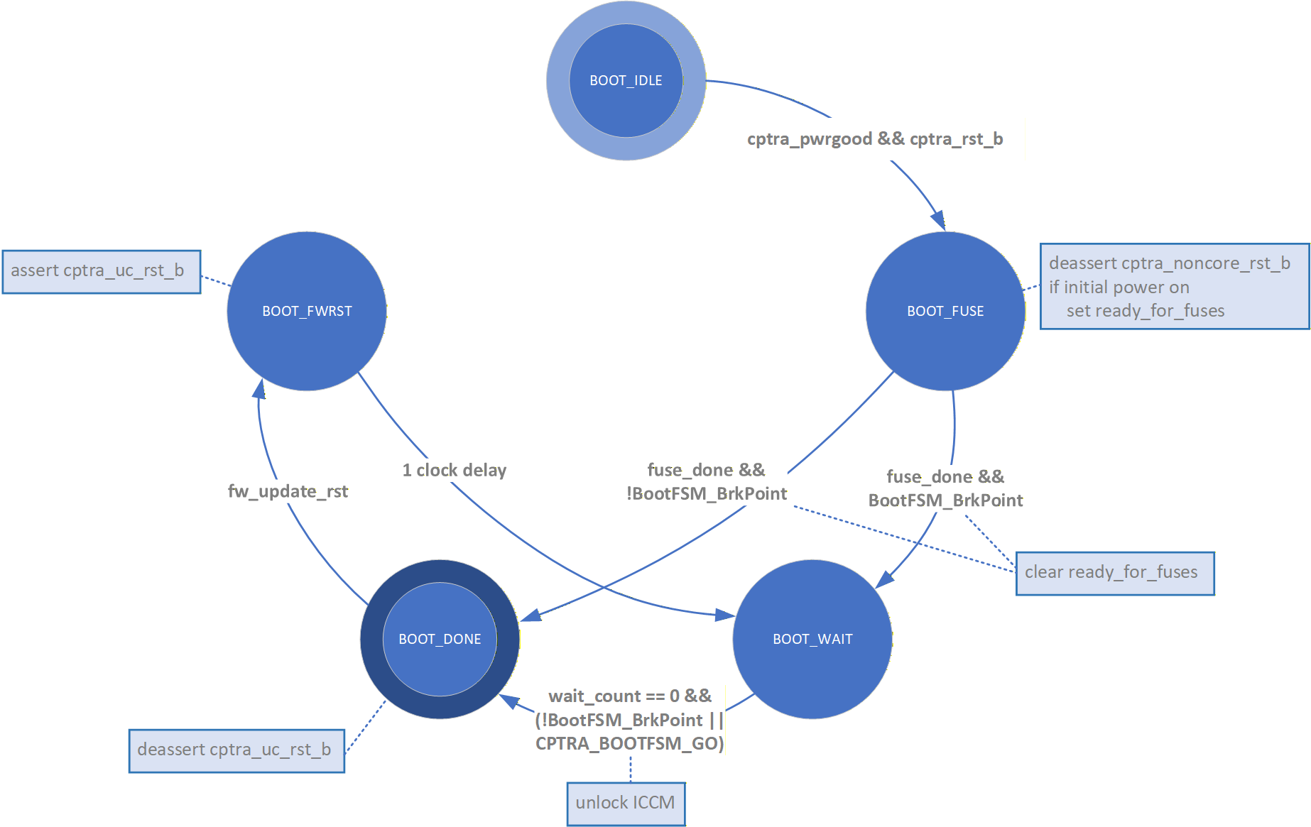
| 51 | +* [Key Vault Boot Flow Transition Enforcement](#key-vault-boot-flow-transition-enforcement) -- HW-enforced DICE key integrity monitoring and slot access control across boot phases | ||
| 52 | + | ||
| 53 | + | ||
| 42 | 54 | ## Boot FSM | |
| 43 | 55 | ||
| 44 | 56 | The Boot FSM detects that the SoC is bringing Caliptra out of reset. Part of this flow involves signaling to the SoC that Caliptra is awake and ready for fuses. After fuses are populated and the SoC indicates that it is done downloading fuses, Caliptra can wake up the rest of the IP by de-asserting the internal reset. | |
| 45 | 57 | ||
| 46 | -The following figure shows the initial power-on arc of the Mailbox Boot FSM. | ||
| 47 | - | ||
| 48 | -*Figure 1: Mailbox Boot FSM state diagram* | ||
| 49 | - | ||
| 50 | - | ||
| 58 | +The following figure shows the state transitions and associated actions in Caliptra's boot state machine. | ||
| 59 | + | ||
| 60 | +*Figure: Caliptra Boot FSM state diagram* | ||
| 61 | + | ||
| 62 | + | ||
| 51 | 63 | ||
| 52 | 64 | The Boot FSM first waits for the SoC to assert cptra\_pwrgood and de-assert cptra\_rst\_b. In the BOOT\_FUSE state, Caliptra signals to the SoC that it is ready for fuses. After the SoC is done writing fuses, it sets the fuse done register and the FSM advances to BOOT\_DONE. | |
| 53 | 65 | ||
| 54 | -BOOT\_DONE enables Caliptra reset de-assertion through a two flip-flop synchronizer. | ||
| 55 | - | ||
| 56 | -## FW update reset (Impactless FW update) | ||
| 57 | - | ||
| 58 | -When a firmware update is initiated, Runtime FW writes to fw\_update\_reset register to trigger the FW update reset. When this register is written, only the RISC-V core is reset using cptra\_uc\_fw\_rst\_b pin and all AHB targets are still active. All registers within the targets and ICCM/DCCM memories are intact after the reset. Reset is deasserted synchronously after a programmable number of cycles; the minimum allowed number of wait cycles is 5, which is also the default configured value. Reset de-assertion is done through a two flip-flop synchronizer. Since ICCM is locked during runtime, the boot FSM unlocks it when the RISC-V reset is asserted. Following FW update reset deassertion, normal boot flow updates the ICCM with the new FW from the mailbox SRAM. The boot flow is modified as shown in the following figure. | ||
| 59 | - | ||
| 60 | -*Figure 2: Mailbox Boot FSM state diagram for FW update reset* | ||
| 61 | - | ||
| 62 | - | ||
| 66 | +Once in the BOOT\_DONE state, Caliptra de-asserts resets through a two flip-flop synchronizer. | ||
| 67 | + | ||
| 68 | +### FW update reset (Impactless FW update) | ||
| 69 | + | ||
| 70 | +When a firmware update is initiated, Runtime FW writes to fw\_update\_reset register to trigger the FW update reset. When this register is written, only the RISC-V core is reset using cptra\_uc\_rst\_b pin and all AHB targets are still active. All registers within the targets and ICCM/DCCM memories are intact after the reset. Reset is deasserted synchronously after a programmable number of cycles; the minimum allowed number of wait cycles is 5, which is also the default configured value. Reset de-assertion is done through a two flip-flop synchronizer. Since ICCM is locked during runtime, the boot FSM unlocks it when the RISC-V reset is asserted. Following FW update reset deassertion, normal boot flow updates the ICCM with the new FW from the mailbox SRAM. | ||
| 63 | 71 | ||
| 64 | 72 | Impactless firmware updates may be initiated by writing to the fw\_update\_reset register after Caliptra comes out of global reset and enters the BOOT\_DONE state. In the BOOT\_FWRST state, only the reset to the RISC-V core is asserted and the wait timer is initialized. After the timer expires, the FSM advances from the BOOT\_WAIT to BOOT\_DONE state where the reset is deasserted and ICCM is unlocked. | |
| 73 | + | ||
| 74 | +### Breakpoints for Debug | ||
| 75 | + | ||
| 76 | +Integrators may connect a breakpoint input to Caliptra, which is intended to connect to a chip GPIO pin. When asserted, this pin causes the Caliptra boot FSM to follow a modified arc. Instead of transitioning immediately to the BOOT_DONE state upon completion of fuse programming, the state machine transitions from BOOT_FUSE to BOOT_WAIT. Here, the state machine halts until the Caliptra register [CPTRA_BOOTFSM_GO](https://chipsalliance.github.io/caliptra-rtl/main/internal-regs/?p=clp.soc_ifc_reg.CPTRA_BOOTFSM_GO) is set, either by AXI or TAP access. | ||
| 65 | 77 | ||
| 66 | 78 | ## RISC-V core | |
| 67 | 79 | ||
| @@ -116,8 +128,9 @@ | |||
| 116 | 128 | | Data Vault | 5 | 8 KiB | 0x1001_C000 | 0x1001_DFFF | | |
| 117 | 129 | | SHA512 | 6 | 32 KiB | 0x1002_0000 | 0x1002_7FFF | | |
| 118 | 130 | | SHA256 | 10 | 32 KiB | 0x1002_8000 | 0x1002_FFFF | | |
| 119 | -| ML-DSA | 14 | 64 KiB | 0x1003_0000 | 0x1003_FFFF | | ||
| 131 | +| ABR (MLDSA/MLKEM) | 14 | 64 KiB | 0x1003_0000 | 0x1003_FFFF | | ||
| 120 | 132 | | AES | 15 | 4 KiB | 0x1001_1000 | 0x1001_1FFF | | |
| 133 | +| SHA3 | 16 | 4 KiB | 0x1004_0000 | 0x1004_0FFF | | ||
| 121 | 134 | ||
| 122 | 135 | ||
| 123 | 136 | #### Peripherals subsystem | |
| @@ -196,8 +209,8 @@ | |||
| 196 | 209 | | Mailbox (Notifications) | 20 | 7 | | |
| 197 | 210 | | SHA512 Accelerator (Errors) | 23 | 8 | | |
| 198 | 211 | | SHA512 Accelerator (Notifications) | 24 | 7 | | |
| 199 | -| MLDSA (Errors) | 23 | 8 | | ||
| 200 | -| MLDSA (Notifications) | 24 | 7 | | ||
| 212 | +| ABR (MLDSA/MLKEM) (Errors) | 23 | 8 | | ||
| 213 | +| ABR (MLDSA/MLKEM) (Notifications) | 24 | 7 | | ||
| 201 | 214 | | AXI DMA (Errors) | 25 | 8 | | |
| 202 | 215 | | AXI DMA (Notifications) | 26 | 7 | | |
| 203 | 216 | ||
| @@ -220,7 +233,7 @@ | |||
| 220 | 233 | ||
| 221 | 234 | The following figure shows the two timers. | |
| 222 | 235 | ||
| 223 | -*Figure 3: Caliptra Watchdog Timer* | ||
| 236 | +*Figure: Caliptra Watchdog Timer* | ||
| 224 | 237 | ||
| 225 | 238 | 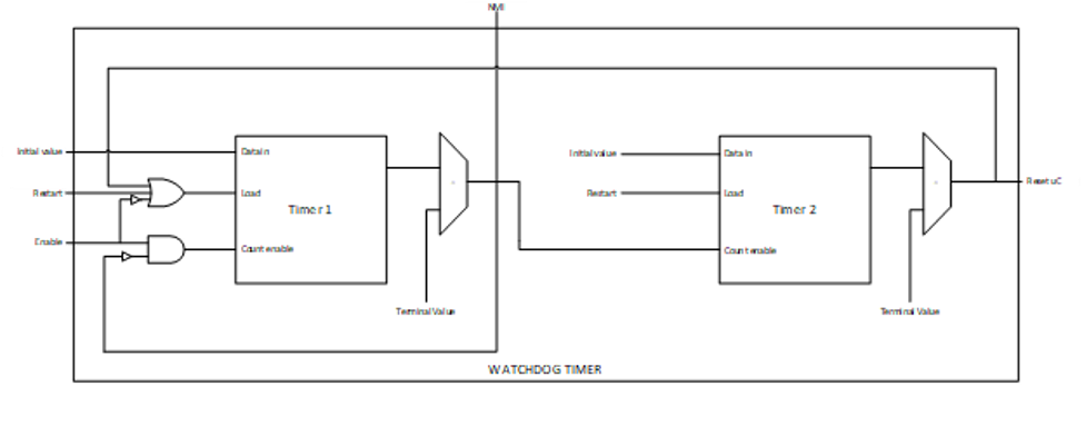 | |
| 226 | 239 | ||
| @@ -358,7 +371,7 @@ | |||
| 358 | 371 | ||
| 359 | 372 | The following figure shows the timing information for clock gating. | |
| 360 | 373 | ||
| 361 | -*Figure 10: Clock gating timing* | ||
| 374 | +*Figure: Clock gating timing* | ||
| 362 | 375 | ||
| 363 | 376 | 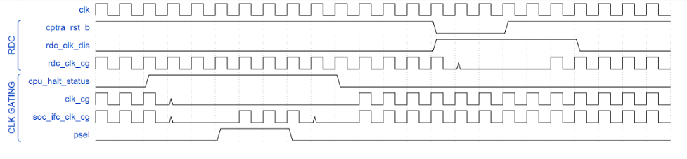 | |
| 364 | 377 | ||
| @@ -372,19 +385,19 @@ | |||
| 372 | 385 | ||
| 373 | 386 | The following figure shows the integrated TRNG block. | |
| 374 | 387 | ||
| 375 | -*Figure 11: Integrated TRNG block* | ||
| 388 | +*Figure: Integrated TRNG block* | ||
| 376 | 389 | ||
| 377 | 390 | 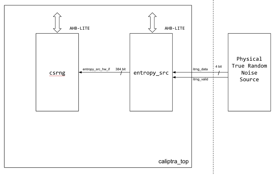 | |
| 378 | 391 | ||
| 379 | 392 | The following figure shows the CSRNG block. | |
| 380 | 393 | ||
| 381 | -*Figure 12: CSRNG block* | ||
| 394 | +*Figure: CSRNG block* | ||
| 382 | 395 | ||
| 383 | 396 | 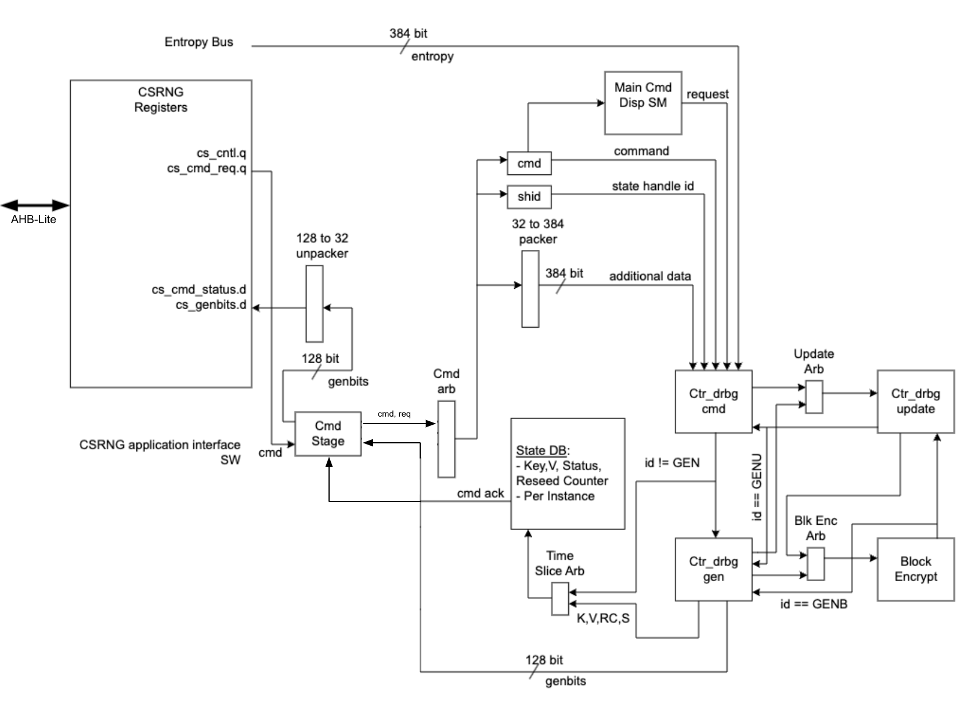 | |
| 384 | 397 | ||
| 385 | 398 | The following figure shows the entropy source block. | |
| 386 | 399 | ||
| 387 | -*Figure 13: Entropy source block* | ||
| 400 | +*Figure: Entropy source block* | ||
| 388 | 401 | ||
| 389 | 402 | 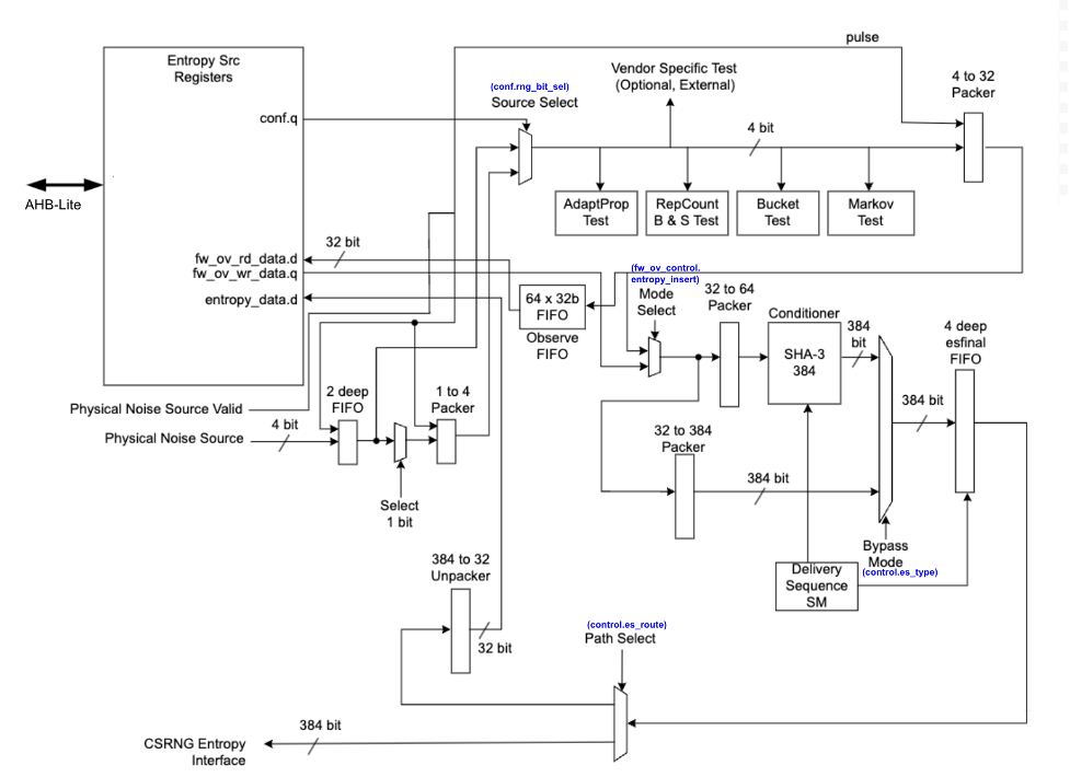 | |
| 390 | 403 | ||
| @@ -450,7 +463,7 @@ | |||
| 450 | 463 | ||
| 451 | 464 | The following figure shows the top level signals defined in caliptra\_top. | |
| 452 | 465 | ||
| 453 | -*Figure 14: caliptra\_top signals* | ||
| 466 | +*Figure: caliptra\_top signals* | ||
| 454 | 467 | ||
| 455 | 468 | 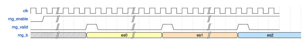 | |
| 456 | 469 | ||
| @@ -472,7 +485,7 @@ | |||
| 472 | 485 | ||
| 473 | 486 | The following figure shows the entropy source signals. | |
| 474 | 487 | ||
| 475 | -*Figure 15: Entropy source signals* | ||
| 488 | +*Figure: Entropy source signals* | ||
| 476 | 489 | ||
| 477 | 490 | 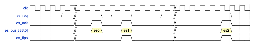 | |
| 478 | 491 | ||
| @@ -634,7 +647,54 @@ | |||
| 634 | 647 | ||
| 635 | 648 | Note: If the debug security state switches to debug mode anytime, the security assets and keys are still flushed even though JTAG is not open. | |
| 636 | 649 | ||
| 637 | -*Figure 16: JTAG implementation* | ||
| 650 | +The following table details the alias addresses for registers in soc ifc that are accessible through JTAG. | ||
| 651 | +Debug Locked registers are a subset of registers accessible when debug intent is set, when debug is unlocked, or the lifecycle state is DEVICE_MANUFACTURING. | ||
| 652 | +Debug Unlocked registers are accessible when debug is unlocked, or the lifecycle state is DEVICE_MANUFACTURING. | ||
| 653 | + | ||
| 654 | +| Register Name | JTAG Address | Accessibility | Debug Locked | Debug Unlocked | | ||
| 655 | +| ------------------------------------------- | -------------- | --------------- | -------------- | ---------------- | | ||
| 656 | +| mbox_lock | 7’h75 | RO | YES | YES | | ||
| 657 | +| mbox_cmd | 7’h76 | RW | YES | YES | | ||
| 658 | +| mbox_dlen | 7’h50 | RW | YES | YES | | ||
| 659 | +| mbox_dataout | 7’h51 | RO | YES | YES | | ||
| 660 | +| mbox_datain | 7’h62 | WO | YES | YES | | ||
| 661 | +| mbox_status | 7’h52 | RW | YES | YES | | ||
| 662 | +| mbox_execute | 7’h77 | WO | YES | YES | | ||
| 663 | +| CPTRA_BOOT_STATUS | 7’h53 | RO | YES | YES | | ||
| 664 | +| CPTRA_HW_ERRROR_ENC | 7’h54 | RO | YES | YES | | ||
| 665 | +| CPTRA_FW_ERROR_ENC | 7’h55 | RO | YES | YES | | ||
| 666 | +| SS_UDS_SEED_BASE_ADDR_L | 7’h56 | RO || YES | | ||
| 667 | +| SS_UDS_SEED_BASE_ADDR_H | 7’h57 | RO || YES | | ||
| 668 | +| CPTRA_HW_ERROR_FATAL | 7’h58 | RO | YES | YES | | ||
| 669 | +| CPTRA_FW_ERROR_FATAL | 7’h59 | RO | YES | YES | | ||
| 670 | +| CPTRA_HW_ERROR_NON_FATAL | 7’h5a | RO | YES | YES | | ||
| 671 | +| CPTRA_FW_ERROR_NON_FATAL | 7’h5b | RO | YES | YES | | ||
| 672 | +| CPTRA_DBG_MANUF_SERVICE_REG | 7’h60 | RW | YES | YES | | ||
| 673 | +| CPTRA_BOOTFSM_GO | 7’h61 | RW | YES | YES | | ||
| 674 | +| SS_DEBUG_INTENT | 7’h63 | RW || YES | | ||
| 675 | +| SS_CALIPTRA_BASE_ADDR_L | 7’h64 | RW || YES | | ||
| 676 | +| SS_CALIPTRA_BASE_ADDR_H | 7’h65 | RW || YES | | ||
| 677 | +| SS_MCI_BASE_ADDR_L | 7’h66 | RW || YES | | ||
| 678 | +| SS_MCI_BASE_ADDR_H | 7’h67 | RW || YES | | ||
| 679 | +| SS_RECOVERY_IFC_BASE_ADDR_L | 7’h68 | RW || YES | | ||
| 680 | +| SS_RECOVERY_IFC_BASE_ADDR_H | 7’h69 | RW || YES | | ||
| 681 | +| SS_OTP_FC_BASE_ADDR_L | 7’h6A | RW || YES | | ||
| 682 | +| SS_OTP_FC_BASE_ADDR_H | 7’h6B | RW || YES | | ||
| 683 | +| SS_STRAP_GENERIC_0 | 7’h6C | RW || YES | | ||
| 684 | +| SS_STRAP_GENERIC_1 | 7’h6D | RW || YES | | ||
| 685 | +| SS_STRAP_GENERIC_2 | 7’h6E | RW || YES | | ||
| 686 | +| SS_STRAP_GENERIC_3 | 7’h6F | RW || YES | | ||
| 687 | +| SS_DBG_SERVICE_REG_REQ | 7’h70 | RW | YES | YES | | ||
| 688 | +| SS_DBG_SERVICE_REG_RSP | 7’h71 | RO | YES | YES | | ||
| 689 | +| SS_DBG_UNLOCK_LEVEL0 | 7’h72 | RW || YES | | ||
| 690 | +| SS_DBG_UNLOCK_LEVEL1 | 7’h73 | RW || YES | | ||
| 691 | +| SS_STRAP_CALIPTRA_DMA_AXI_USER | 7’h74 | RW || YES | | ||
| 692 | +| SS_EXTERNAL_STAGING_AREA_BASE_ADDR_L | 7’h78 | RW || YES | | ||
| 693 | +| SS_EXTERNAL_STAGING_AREA_BASE_ADDR_H | 7’h79 | RW || YES | | ||
| 694 | + | ||
| 695 | + | ||
| 696 | + | ||
| 697 | +*Figure: JTAG implementation* | ||
| 638 | 698 | ||
| 639 | 699 |  | |
| 640 | 700 | ||
| @@ -644,18 +704,19 @@ | |||
| 644 | 704 | ||
| 645 | 705 | * Symmetric cryptographic primitives | |
| 646 | 706 | * De-obfuscation engine | |
| 647 | - * SHA512/384 (based on NIST FIPS 180-4 [2]) | ||
| 648 | - * SHA256 (based on NIST FIPS 180-4 [2]) | ||
| 649 | - * HMAC512 (based on [NIST FIPS 198-1](https://nvlpubs.nist.gov/nistpubs/FIPS/NIST.FIPS.198-1.pdf) [5] and [RFC 4868](https://tools.ietf.org/html/rfc4868) [6]) | ||
| 707 | + * SHA512/384 (based on NIST FIPS 180-4 [2]) | ||
| 708 | + * SHA256 (based on NIST FIPS 180-4 [2]) | ||
| 709 | + * HMAC512 (based on [NIST FIPS 198-1](https://nvlpubs.nist.gov/nistpubs/FIPS/NIST.FIPS.198-1.pdf) [5] and [RFC 4868](https://tools.ietf.org/html/rfc4868) [6]) | ||
| 710 | + * SHA3 (based on [NIST FIPS 202](https://doi.org/10.6028/NIST.FIPS.202) [17]) | ||
| 650 | 711 | * Public-key cryptography | |
| 651 | - * NIST Secp384r1 Deterministic Digital Signature Algorithm (based on FIPS-186-4 [11] and RFC 6979 [7]) | ||
| 712 | + * NIST Secp384r1 Deterministic Digital Signature Algorithm (based on FIPS-186-4 [11] and RFC 6979 [7]) | ||
| 652 | 713 | * Key vault | |
| 653 | - * Key slots | ||
| 654 | - * Key slot management | ||
| 714 | + * Key slots | ||
| 715 | + * Key slot management | ||
| 655 | 716 | ||
| 656 | 717 | The high-level architecture of Caliptra cryptographic subsystem is shown in the following figure. | |
| 657 | 718 | ||
| 658 | -*Figure 17: Caliptra cryptographic subsystem* | ||
| 719 | +*Figure: Caliptra cryptographic subsystem* | ||
| 659 | 720 | ||
| 660 | 721 |  | |
| 661 | 722 | ||
| @@ -680,7 +741,7 @@ | |||
| 680 | 741 | ||
| 681 | 742 | The total size should be equal to 128 bits short of a multiple of 1024 since the goal is to have the formatted message size as a multiple of 1024 bits (N x 1024). The following figure shows the SHA512 input formatting. | |
| 682 | 743 | ||
| 683 | -*Figure 18: SHA512 input formatting* | ||
| 744 | +*Figure: SHA512 input formatting* | ||
| 684 | 745 | ||
| 685 | 746 |  | |
| 686 | 747 | ||
| @@ -692,7 +753,7 @@ | |||
| 692 | 753 | ||
| 693 | 754 | The SHA512 architecture has the finite-state machine as shown in the following figure. | |
| 694 | 755 | ||
| 695 | -*Figure 19: SHA512 FSM* | ||
| 756 | +*Figure: SHA512 FSM* | ||
| 696 | 757 | ||
| 697 | 758 | 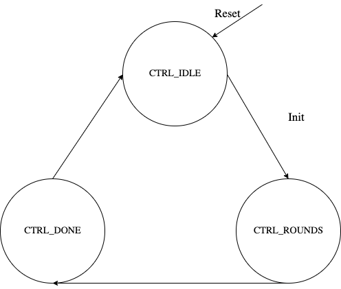 | |
| 698 | 759 | ||
| @@ -716,13 +777,13 @@ | |||
| 716 | 777 | ||
| 717 | 778 | ### Address map | |
| 718 | 779 | ||
| 719 | -The SHA512 address map is shown here: [sha512\_reg — clp Reference (chipsalliance.github.io)](https://chipsalliance.github.io/caliptra-rtl/main/internal-regs/?p=clp.sha512_reg) | ||
| 780 | +The SHA512 address map is shown here: [sha512\_reg -- clp Reference (chipsalliance.github.io)](https://chipsalliance.github.io/caliptra-rtl/main/internal-regs/?p=clp.sha512_reg) | ||
| 720 | 781 | ||
| 721 | 782 | ### Pseudocode | |
| 722 | 783 | ||
| 723 | 784 | The following pseudocode demonstrates how the SHA512 interface can be implemented. | |
| 724 | 785 | ||
| 725 | -*Figure 20: SHA512 pseudocode* | ||
| 786 | +*Figure: SHA512 pseudocode* | ||
| 726 | 787 | ||
| 727 | 788 | 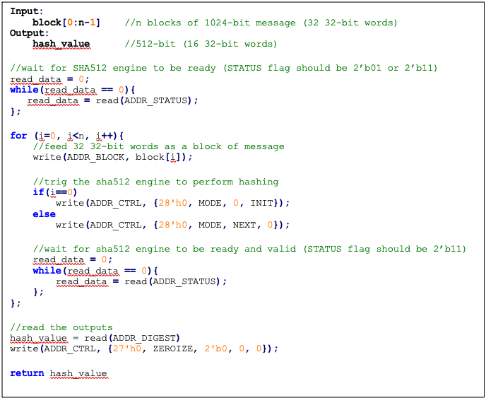 | |
| 728 | 789 | ||
| @@ -803,7 +864,7 @@ | |||
| 803 | 864 | ||
| 804 | 865 | The following figure shows SHA256 input formatting. | |
| 805 | 866 | ||
| 806 | -*Figure 21: SHA256 input formatting* | ||
| 867 | +*Figure: SHA256 input formatting* | ||
| 807 | 868 | ||
| 808 | 869 | 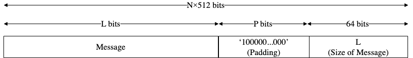 | |
| 809 | 870 | ||
| @@ -815,7 +876,7 @@ | |||
| 815 | 876 | ||
| 816 | 877 | The SHA256 architecture has the finite-state machine as shown in the following figure. | |
| 817 | 878 | ||
| 818 | -*Figure 22: SHA256 FSM* | ||
| 879 | +*Figure: SHA256 FSM* | ||
| 819 | 880 | ||
| 820 | 881 | 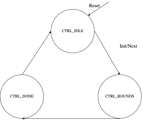 | |
| 821 | 882 | ||
| @@ -844,13 +905,13 @@ | |||
| 844 | 905 | ||
| 845 | 906 | ### Address map | |
| 846 | 907 | ||
| 847 | -The SHA256 address map is shown here: [sha256\_reg — clp Reference (chipsalliance.github.io)](https://chipsalliance.github.io/caliptra-rtl/main/internal-regs/?p=clp.sha256_reg). | ||
| 908 | +The SHA256 address map is shown here: [sha256\_reg -- clp Reference (chipsalliance.github.io)](https://chipsalliance.github.io/caliptra-rtl/main/internal-regs/?p=clp.sha256_reg). | ||
| 848 | 909 | ||
| 849 | 910 | ### Pseudocode | |
| 850 | 911 | ||
| 851 | 912 | The following pseudocode demonstrates how the SHA256 interface can be implemented. | |
| 852 | 913 | ||
| 853 | -*Figure 23: SHA256 pseudocode* | ||
| 914 | +*Figure: SHA256 pseudocode* | ||
| 854 | 915 | ||
| 855 | 916 | 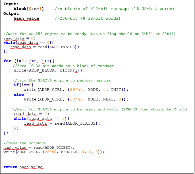 | |
| 856 | 917 | ||
| @@ -890,6 +951,164 @@ | |||
| 890 | 951 | | 1 KiB message | 8761 | 21.90 | 45,657 | | |
| 891 | 952 | ||
| 892 | 953 | ||
| 954 | +## SHA3 | ||
| 955 | + | ||
| 956 | +The SHA3 HWIP performs the hash functions, whose purpose is to check the integrity of the received message. | ||
| 957 | +It supports various SHA3 hashing functions including SHA3 Extended Output Function (XOF) known as SHAKE functions. | ||
| 958 | +The details of the operation are described in the [SHA3 specification, FIPS 202](https://csrc.nist.gov/publications/detail/fips/202/final) known as _sponge construction_. | ||
| 959 | +It has been adapted from OpenTitan and you can find documentation describing the functionality of the KMAC block it was derived from [here](https://opentitan.org/book/hw/ip/kmac/index.html). | ||
| 960 | +In the current use cases of the SHA3 HW IP, either (a) messages are not considered secret (External Mu), or (b) SCA hardening would not be meaningful (HPKE in OCP L.O.C.K.), hence there are no SCA requirements. | ||
| 961 | + | ||
| 962 | +### Features | ||
| 963 | +- Support for SHA3-224, 256, 384, 512, SHAKE[128, 256] and cSHAKE[128, 256] | ||
| 964 | +- Support byte-granularity on input message | ||
| 965 | +- Support arbitrary output length for SHAKE, cSHAKE | ||
| 966 | +- Support customization input string S, and function-name N up to 36 bytes total | ||
| 967 | +- 64b x 10 depth Message FIFO | ||
| 968 | +- Performance (at 100 MHz): | ||
| 969 | + - SHA3-224: 2.93 B/cycle, 2.34 Gbit/s - 1.19 B/cycle, 952 Mbit/s (DOM) | ||
| 970 | + - SHA3-512: 1.47 B/cycle, 1.18 Gbit/s - 0.59 B/cycle, 472 Mbit/s (DOM) | ||
| 971 | + | ||
| 972 | +### Design Details | ||
| 973 | + | ||
| 974 | +#### Keccak Round | ||
| 975 | + | ||
| 976 | +A Keccak round implements the Keccak_f function described in the SHA3 specification. | ||
| 977 | +Keccak round logic in SHA3 HWIP not only supports 1600 bit internal states but also all possible values {25, 50, 100, 200, 400, 800, 1600} based on a parameter `Width`. | ||
| 978 | +Keccak permutations in the specification allow arbitrary number of rounds. | ||
| 979 | +This module, however, supports Keccak_f which always runs `12 + 2*L` rounds, where \\[ L = log_2 {( {Width \over 25} )} \\] . | ||
| 980 | +For instance, 200 bits of internal state run 18 rounds. | ||
| 981 | +SHA3 instantiates the Keccak round module with 1600 bit. | ||
| 982 | + | ||
| 983 | + | ||
| 984 | + | ||
| 985 | +Keccak round logic has two phases inside. | ||
| 986 | +Theta, Rho, Pi functions are executed at the 1st phase. | ||
| 987 | +Chi and Iota functions run at the 2nd phase. | ||
| 988 | +The first phase and the second phase run in the same cycle. | ||
| 989 | + | ||
| 990 | +To save circuit area, the Chi function uses 800 instead 1600 DOM multipliers but the multipliers are fully pipelined. | ||
| 991 | +The Chi and Iota functions are thus separately applied to the two halves of the state and the 2nd phase takes in total three clock cycles to complete. | ||
| 992 | +In the first clock cycle of the 2nd phase, the first stage of Chi is computed for the first lane halves of the state. | ||
| 993 | +In the second clock cycle, the new first lane halves are output and written to state register. | ||
| 994 | +At the same time, the first stage of Chi is computed for the second lane halves. | ||
| 995 | +In the third clock cycle, the new second lane halves are output and written to the state register. | ||
| 996 | + | ||
| 997 | +#### Padding for Keccak | ||
| 998 | + | ||
| 999 | +Padding logic supports SHA3/SHAKE/cSHAKE algorithms. | ||
| 1000 | +cSHAKE needs the extra inputs for the Function-name `N` and the Customization string `S`. | ||
| 1001 | +Other than that, SHA3, SHAKE, and cSHAKE share similar datapath inside the padding module except the last part added next to the end of the message. | ||
| 1002 | +SHA3 adds `2'b 10`, SHAKE adds `4'b 1111`, cSHAKE adds `2'b00` then `pad10*1()` follows. | ||
| 1003 | +All are little-endian values. | ||
| 1004 | + | ||
| 1005 | +Interface between this padding logic and the MSG_FIFO follows the conventional FIFO interface. | ||
| 1006 | +So `caliptra_prim_fifo_*` can talk to the padding logic directly. | ||
| 1007 | +This module talks to Keccak round logic with a more memory-like interface. | ||
| 1008 | +The interface has an additional address signal on top of the valid, ready, and data signals. | ||
| 1009 | + | ||
| 1010 | + | ||
| 1011 | + | ||
| 1012 | +The hashing process begins when the software issues the start command to `CMD` . | ||
| 1013 | +If cSHAKE is enabled, the padding logic expands the prefix value (`N || S` above) into a block size. | ||
| 1014 | +The block size is determined by the `CFG_SHADOWED.kstrength`. | ||
| 1015 | +If the value is 128, the block size will be 168 bytes. | ||
| 1016 | +If it is 256, the block size will be 136 bytes. | ||
| 1017 | +The expanded prefix value is transmitted to the Keccak round logic. | ||
| 1018 | +After sending the block size, the padding logic triggers the Keccak round logic to run a full 24 rounds. | ||
| 1019 | + | ||
| 1020 | +If the mode is not cSHAKE, or cSHAKE mode and the prefix block has been processed, the padding logic accepts the incoming message bitstream and forward the data to the Keccak round logic in a block granularity. | ||
| 1021 | +The padding logic controls the data flow and makes the Keccak logic to run after sending a block size. | ||
| 1022 | + | ||
| 1023 | +After the software writes the message bitstream, it should issue the Process command into `CMD` register. | ||
| 1024 | +The padding logic, after receiving the Process command, appends proper ending bits with respect to the `CFG_SHADOWED.mode` value. | ||
| 1025 | +The logic writes 0 up to the block size to the Keccak round logic then ends with 1 at the end of the block. | ||
| 1026 | + | ||
| 1027 | + | ||
| 1028 | + | ||
| 1029 | +After the Keccak round completes the last block, the padding logic asserts an `absorbed` signal to notify the software. | ||
| 1030 | +At this point, the software is able to read the digest in `STATE` memory region. | ||
| 1031 | +If the output length is greater than the Keccak block rate in SHAKE and cSHAKE mode, the software may run the Keccak round manually by issuing Run command to `CMD` register. | ||
| 1032 | + | ||
| 1033 | +The software completes the operation by issuing Done command after reading the digest. | ||
| 1034 | +The padding logic clears internal variables and goes back to Idle state. | ||
| 1035 | + | ||
| 1036 | +#### Message FIFO | ||
| 1037 | + | ||
| 1038 | +The SHA3 HWIP has a compile-time configurable depth message FIFO inside. | ||
| 1039 | +The message FIFO receives incoming message bitstream regardless of its byte position in a word. | ||
| 1040 | +Then it packs the partial message bytes into the internal 64 bit data width. | ||
| 1041 | +After packing the data, the logic stores the data into the FIFO until the internal SHA3 engine consumes the data. | ||
| 1042 | + | ||
| 1043 | +##### FIFO Depth calculation | ||
| 1044 | + | ||
| 1045 | +The depth of the message FIFO is chosen to cover the throughput of the software or other producers such as DMA engine. | ||
| 1046 | +The size of the message FIFO is enough to hold the incoming data while the SHA3 engine is processing the previous block. | ||
| 1047 | +Default design parameters assume the system characteristics as below: | ||
| 1048 | + | ||
| 1049 | +- `kmac_pkg::RegLatency`: The register write takes 5 cycles. | ||
| 1050 | +- `kmac_pkg::Sha3Latency`: Keccak round latency takes 24 cycles. | ||
| 1051 | + | ||
| 1052 | +##### Empty and Full status | ||
| 1053 | + | ||
| 1054 | +Under normal operating conditions, the SHA3 engine will process data a lot faster than software can push it to the Message FIFO. | ||
| 1055 | +The Message FIFO depth observable from `STATUS.fifo_depth` will remain **0** while the `STATUS.fifo_empty` status bit is lowered for one clock cycle whenever software provides new data. | ||
| 1056 | + | ||
| 1057 | +After the SHA3 engine starts popping the data again, the Message FIFO will eventually run empty again and the `fifo_empty` status interrupt will fire. | ||
| 1058 | +Note that the `fifo_empty` status interrupt will not fire if i) one of the hardware application interfaces is using the SHA3 block, ii) the SHA3 core is not in the `Absorb` state, or iii) after software has written the `Process` command. | ||
| 1059 | + | ||
| 1060 | +If software pushes data to the Message FIFO while it is full, the write operation is blocked until there is again space in the FIFO. | ||
| 1061 | +This means the processor is effectively stalled. | ||
| 1062 | +If the SHA3 engine is currently running and software fills up the Message FIFO, the resulting stall won't take more than 100 clock cycles. | ||
| 1063 | +The stall mechanism prevents data loss and the upper bound on the wait time avoids software needing to poll the `STATUS.fifo_depth` field before writing data. | ||
| 1064 | + | ||
| 1065 | +### Programmer's guide | ||
| 1066 | + | ||
| 1067 | +The software can update the SHA3 configurations only when the IP is in the idle state. | ||
| 1068 | +The software should check `STATUS.sha3_idle` before updating the configurations. | ||
| 1069 | +The software must first program `CFG_SHADOWED.msg_endianness` and `CFG_SHADOWED.state_endianness` at the initialization stage. | ||
| 1070 | +These determine the byte order of incoming messages (msg_endianness) and the Keccak state output (state_endianness). | ||
| 1071 | + | ||
| 1072 | +#### Software Initiated SHA3 process | ||
| 1073 | + | ||
| 1074 | +This section describes the expected software process to run the SHA3 HWIP. | ||
| 1075 | +At first, the software configures `CFG_SHADOWED.kmac_en` for the operation. | ||
| 1076 | +If SHA3 is enabled, the software should configure `CFG_SHADOWED.mode` to cSHAKE and `CFG_SHADOWED.kstrength` to 128 or 256 bit security strength. | ||
| 1077 | +The software also updates `PREFIX` registers if cSHAKE mode is used. | ||
| 1078 | +Current design does not convert cSHAKE mode to SHAKE even if `PREFIX` is empty string. | ||
| 1079 | +It is the software's responsibility to change the `CFG_SHADOWED.mode` to SHAKE in case of empty `PREFIX`. | ||
| 1080 | +The SHA3 HWIP uses `PREFIX` registers as it is. | ||
| 1081 | +It means that the software should update `PREFIX` with encoded values. | ||
| 1082 | + | ||
| 1083 | +After configuring, the software notifies the SHA3 engine to accept incoming messages by issuing Start command into `CMD`. | ||
| 1084 | +If Start command is not issued, the incoming message is discarded. | ||
| 1085 | + | ||
| 1086 | +After the software pushes all messages, it issues Process command to `CMD` for SHA3 engine to complete the sponge absorbing process. | ||
| 1087 | +SHA3 hashing engine pads the incoming message as defined in the SHA3 specification. | ||
| 1088 | + | ||
| 1089 | +After the SHA3 engine completes the sponge absorbing step, it generates `kmac_done` interrupt. | ||
| 1090 | +Or the software can poll the `STATUS.squeeze` bit until it becomes 1. | ||
| 1091 | +In this stage, the software may run the Keccak round manually. | ||
| 1092 | + | ||
| 1093 | +If the desired digest length is greater than the Keccak rate, the software issues Run command for the Keccak round logic to run one full round after the software reads the current available Keccak state. | ||
| 1094 | +At this stage, SHA3 does not raise an interrupt when the Keccak round completes the software initiated manual run. | ||
| 1095 | +The software should check `STATUS.squeeze` register field for the readiness of `STATE` value. | ||
| 1096 | + | ||
| 1097 | +After the software reads all the digest values, it issues Done command to `CMD` register to clear the internal states. | ||
| 1098 | +Done command clears the Keccak state, FSM in SHA3, and a few internal variables. | ||
| 1099 | + | ||
| 1100 | +#### Endianness | ||
| 1101 | + | ||
| 1102 | +This SHA3 HWIP operates in little-endian. | ||
| 1103 | +Internal SHA3 hashing engine receives in 64-bit granularity. | ||
| 1104 | +The data written to SHA3 is assumed to be little endian. | ||
| 1105 | + | ||
| 1106 | +The software may write/read the data in big-endian order if `CFG_SHADOWED.msg_endianness` or `CFG_SHADOWED.state_endianness` is set. | ||
| 1107 | +If the endianness bit is 1, the data is assumed to be big-endian. | ||
| 1108 | +So, the internal logic byte-swap the data. | ||
| 1109 | +For example, when the software writes `0xDEADBEEF` with endianness as 1, the logic converts it to `0xEFBEADDE` then writes into MSG_FIFO. | ||
| 1110 | + | ||
| 1111 | + | ||
| 893 | 1112 | ## HMAC512/HMAC384 | |
| 894 | 1113 | ||
| 895 | 1114 | Hash-based message authentication code (HMAC) is a cryptographic authentication technique that uses a hash function and a secret key. HMAC involves a cryptographic hash function and a secret cryptographic key. This implementation supports the HMAC512 variants HMAC-SHA-512-256 and HMAC-SHA-384-192 as specified in [NIST FIPS 198-1](https://nvlpubs.nist.gov/nistpubs/FIPS/NIST.FIPS.198-1.pdf) [5]. The implementation is compatible with the HMAC-SHA-512-256 and HMAC-SHA-384-192 authentication and integrity functions defined in [RFC 4868](https://tools.ietf.org/html/rfc4868) [6]. | |
| @@ -916,25 +1135,25 @@ | |||
| 916 | 1135 | ||
| 917 | 1136 | The total size should be equal to 128 bits, short of a multiple of 1024 because the goal is to have the formatted message size as a multiple of 1024 bits (N x 1024). | |
| 918 | 1137 | ||
| 919 | -*Figure 24: HMAC input formatting* | ||
| 1138 | +*Figure: HMAC input formatting* | ||
| 920 | 1139 | ||
| 921 | 1140 |  | |
| 922 | 1141 | ||
| 923 | 1142 | The following figures show examples of input formatting for different message lengths. | |
| 924 | 1143 | ||
| 925 | -*Figure 25: Message length of 1023 bits* | ||
| 1144 | +*Figure: Message length of 1023 bits* | ||
| 926 | 1145 | ||
| 927 | 1146 |  | |
| 928 | 1147 | ||
| 929 | 1148 | When the message is 1023 bits long, padding is given in the next block along with message size. | |
| 930 | 1149 | ||
| 931 | -*Figure 26: 1 bit padding* | ||
| 1150 | +*Figure: 1 bit padding* | ||
| 932 | 1151 | ||
| 933 | 1152 | 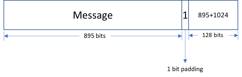 | |
| 934 | 1153 | ||
| 935 | 1154 | When the message size is 895 bits, a padding of ‘1’ is also considered valid, followed by the message size. | |
| 936 | 1155 | ||
| 937 | -*Figure 27: Multi block message* | ||
| 1156 | +*Figure: Multi block message* | ||
| 938 | 1157 | ||
| 939 | 1158 | 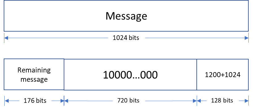 | |
| 940 | 1159 | ||
| @@ -945,13 +1164,13 @@ | |||
| 945 | 1164 | ||
| 946 | 1165 | The HMAC512 core performs the sha2-512 function to process the hash value of the given message. The algorithm processes each block of the 1024 bits from the message, using the result from the previous block. This data flow is shown in the following figure. | |
| 947 | 1166 | ||
| 948 | -*Figure 28: HMAC-SHA-512-256 data flow* | ||
| 1167 | +*Figure: HMAC-SHA-512-256 data flow* | ||
| 949 | 1168 | ||
| 950 | 1169 | 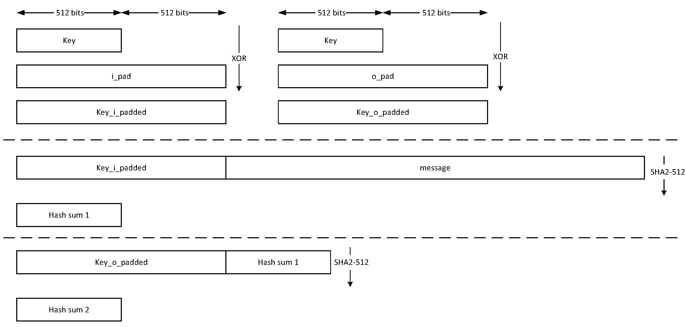 | |
| 951 | 1170 | ||
| 952 | 1171 | The HMAC384 core performs the sha2-384 function to process the hash value of the given message. The algorithm processes each block of the 1024 bits from the message, using the result from the previous block. This data flow is shown in the following figure. | |
| 953 | 1172 | ||
| 954 | -*Figure 29: HMAC-SHA-384-192 data flow* | ||
| 1173 | +*Figure: HMAC-SHA-384-192 data flow* | ||
| 955 | 1174 | ||
| 956 | 1175 | 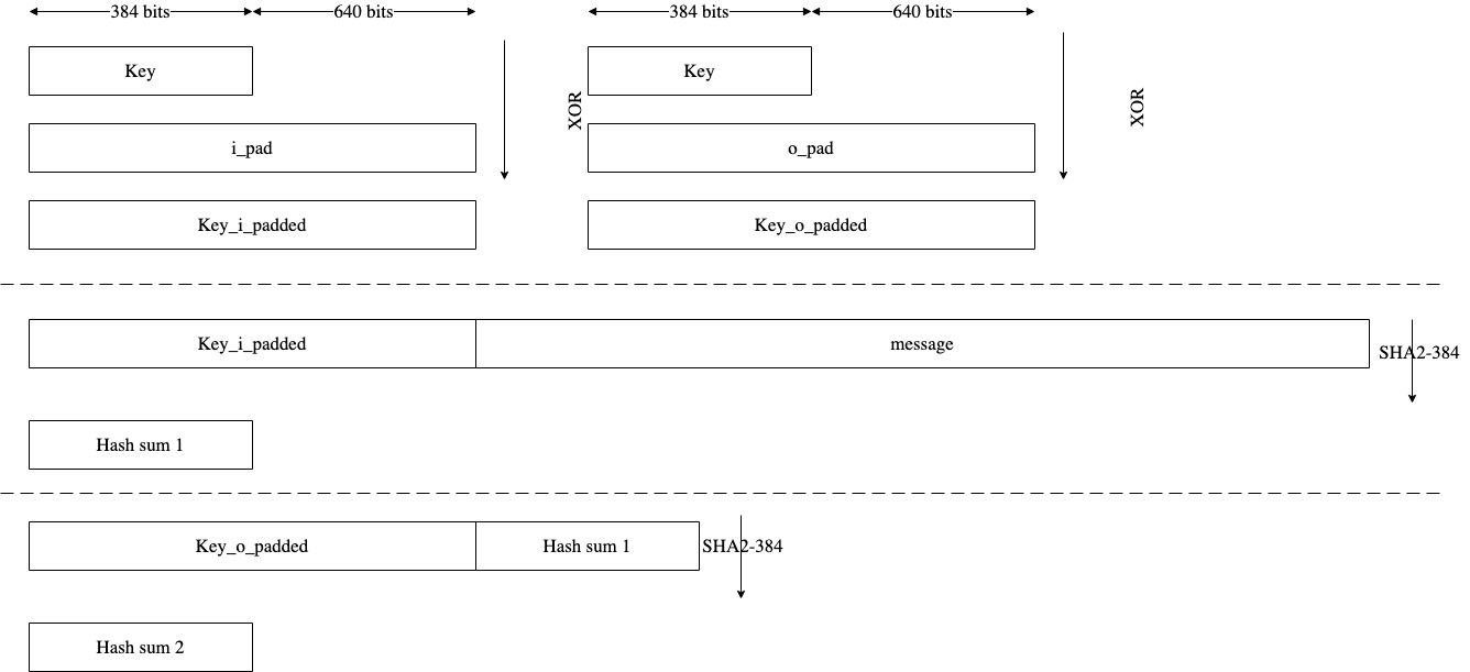 | |
| 957 | 1176 | ||
| @@ -959,7 +1178,7 @@ | |||
| 959 | 1178 | ||
| 960 | 1179 | The HMAC architecture has the finite-state machine as shown in the following figure. | |
| 961 | 1180 | ||
| 962 | -*Figure 30: HMAC FSM* | ||
| 1181 | +*Figure: HMAC FSM* | ||
| 963 | 1182 | ||
| 964 | 1183 |  | |
| 965 | 1184 | ||
| @@ -991,13 +1210,13 @@ | |||
| 991 | 1210 | ||
| 992 | 1211 | ### Address map | |
| 993 | 1212 | ||
| 994 | -The HMAC address map is shown here: [hmac\_reg — clp Reference (chipsalliance.github.io)](https://chipsalliance.github.io/caliptra-rtl/main/internal-regs/?p=clp.hmac_reg). | ||
| 1213 | +The HMAC address map is shown here: [hmac\_reg -- clp Reference (chipsalliance.github.io)](https://chipsalliance.github.io/caliptra-rtl/main/internal-regs/?p=clp.hmac_reg). | ||
| 995 | 1214 | ||
| 996 | 1215 | ### Pseudocode | |
| 997 | 1216 | ||
| 998 | 1217 | The following pseudocode demonstrates how the HMAC interface can be implemented. | |
| 999 | 1218 | ||
| 1000 | -*Figure 31: HMAC pseudocode* | ||
| 1219 | +*Figure: HMAC pseudocode* | ||
| 1001 | 1220 | ||
| 1002 | 1221 |  | |
| 1003 | 1222 | ||
| @@ -1122,7 +1341,7 @@ | |||
| 1122 | 1341 | ||
| 1123 | 1342 | Secp384r1 parameters are shown in the following figure. | |
| 1124 | 1343 | ||
| 1125 | -*Figure 32: Secp384r1 parameters* | ||
| 1344 | +*Figure: Secp384r1 parameters* | ||
| 1126 | 1345 | ||
| 1127 | 1346 |  | |
| 1128 | 1347 | ||
| @@ -1130,7 +1349,7 @@ | |||
| 1130 | 1349 | ||
| 1131 | 1350 | The ECDSA consists of three operations, shown in the following figure. | |
| 1132 | 1351 | ||
| 1133 | -*Figure 33: ECDSA operations* | ||
| 1352 | +*Figure: ECDSA operations* | ||
| 1134 | 1353 | ||
| 1135 | 1354 |  | |
| 1136 | 1355 | ||
| @@ -1175,7 +1394,7 @@ | |||
| 1175 | 1394 | ||
| 1176 | 1395 | The ECC top-level architecture is shown in the following figure. | |
| 1177 | 1396 | ||
| 1178 | -*Figure 34: ECC architecture* | ||
| 1397 | +*Figure: ECC architecture* | ||
| 1179 | 1398 | ||
| 1180 | 1399 |  | |
| 1181 | 1400 | ||
| @@ -1207,7 +1426,7 @@ | |||
| 1207 | 1426 | ||
| 1208 | 1427 | ### Address map | |
| 1209 | 1428 | ||
| 1210 | -The ECC address map is shown here: [ecc\_reg — clp Reference (chipsalliance.github.io)](https://chipsalliance.github.io/caliptra-rtl/main/internal-regs/?p=clp.ecc_reg). | ||
| 1429 | +The ECC address map is shown here: [ecc\_reg -- clp Reference (chipsalliance.github.io)](https://chipsalliance.github.io/caliptra-rtl/main/internal-regs/?p=clp.ecc_reg). | ||
| 1211 | 1430 | ||
| 1212 | 1431 | ### Pseudocode | |
| 1213 | 1432 | ||
| @@ -1215,25 +1434,25 @@ | |||
| 1215 | 1434 | ||
| 1216 | 1435 | #### KeyGen | |
| 1217 | 1436 | ||
| 1218 | -*Figure 35: KeyGen pseudocode* | ||
| 1437 | +*Figure: KeyGen pseudocode* | ||
| 1219 | 1438 | ||
| 1220 | 1439 |  | |
| 1221 | 1440 | ||
| 1222 | 1441 | #### Signing | |
| 1223 | 1442 | ||
| 1224 | -*Figure 36: Signing pseudocode* | ||
| 1443 | +*Figure: Signing pseudocode* | ||
| 1225 | 1444 | ||
| 1226 | 1445 |  | |
| 1227 | 1446 | ||
| 1228 | 1447 | #### Verifying | |
| 1229 | 1448 | ||
| 1230 | -*Figure 37: Verifying pseudocode* | ||
| 1449 | +*Figure: Verifying pseudocode* | ||
| 1231 | 1450 | ||
| 1232 | 1451 |  | |
| 1233 | 1452 | ||
| 1234 | 1453 | #### ECDH sharedkey | |
| 1235 | 1454 | ||
| 1236 | -*Figure 38: ECDH sharedkey pseudocode* | ||
| 1455 | +*Figure: ECDH sharedkey pseudocode* | ||
| 1237 | 1456 | ||
| 1238 | 1457 |  | |
| 1239 | 1458 | ||
| @@ -1299,7 +1518,7 @@ | |||
| 1299 | 1518 | 2. KEYGEN PRIVKEY: Running HMAC\_DRBG with seed and nonce to generate the privkey in KEYGEN operation. | |
| 1300 | 1519 | 3. SIGNING NONCE: Running HMAC\_DRBG based on RFC6979 in SIGNING operation with privkey and hashed\_msg. | |
| 1301 | 1520 | ||
| 1302 | -*Figure 39: HMAC\_DRBG utilization* | ||
| 1521 | +*Figure: HMAC\_DRBG utilization* | ||
| 1303 | 1522 | ||
| 1304 | 1523 |  | |
| 1305 | 1524 | ||
| @@ -1315,7 +1534,7 @@ | |||
| 1315 | 1534 | ||
| 1316 | 1535 | The data flow of the HMAC\_DRBG operation in keygen operation mode is shown in the following figure. | |
| 1317 | 1536 | ||
| 1318 | -*Figure 40: HMAC\_DRBG data flow* | ||
| 1537 | +*Figure: HMAC\_DRBG data flow* | ||
| 1319 | 1538 | ||
| 1320 | 1539 |  | |
| 1321 | 1540 | ||
| @@ -1325,7 +1544,7 @@ | |||
| 1325 | 1544 | ||
| 1326 | 1545 | In practice, observing a t-value greater than a specific threshold (mainly 4.5) indicates the presence of leakage. However, in ECC, due to its latency, around 5 million samples are required to be captured. This latency leads to many false positives and the TVLA threshold can be considered a higher value than 4.5. Based on the following figure from “Side-Channel Analysis and Countermeasure Design for Implementation of Curve448 on Cortex-M4” by Bisheh-Niasar et. al., the threshold can be considered equal to 7 in our case. | |
| 1327 | 1546 | ||
| 1328 | -*Figure 41: TVLA threshold as a function of the number of samples per trace* | ||
| 1547 | +*Figure: TVLA threshold as a function of the number of samples per trace* | ||
| 1329 | 1548 | ||
| 1330 | 1549 |  | |
| 1331 | 1550 | ||
| @@ -1335,7 +1554,7 @@ | |||
| 1335 | 1554 | The TVLA results for performing seed/nonce-dependent leakage detection using 200,000 traces is shown in the following figure. Based on this figure, there is no leakage in ECC keygen by changing the seed/nonce after 200,000 operations. | |
| 1336 | 1555 | ||
| 1337 | 1556 | ||
| 1338 | -*Figure 42: seed/nonce-dependent leakage detection using TVLA for ECC keygen after 200,000 traces* | ||
| 1557 | +*Figure: seed/nonce-dependent leakage detection using TVLA for ECC keygen after 200,000 traces* | ||
| 1339 | 1558 | ||
| 1340 | 1559 |  | |
| 1341 | 1560 | ||
| @@ -1343,13 +1562,13 @@ | |||
| 1343 | 1562 | ||
| 1344 | 1563 | The TVLA results for performing privkey-dependent leakage detection using 20,000 traces is shown in the following figure. Based on this figure, there is no leakage in ECC signing by changing the privkey after 20,000 operations. | |
| 1345 | 1564 | ||
| 1346 | -*Figure 43: privkey-dependent leakage detection using TVLA for ECC signing after 20,000 traces* | ||
| 1565 | +*Figure: privkey-dependent leakage detection using TVLA for ECC signing after 20,000 traces* | ||
| 1347 | 1566 | ||
| 1348 | 1567 |  | |
| 1349 | 1568 | ||
| 1350 | 1569 | The TVLA results for performing message-dependent leakage detection using 64,000 traces is shown in the following figure. Based on this figure, there is no leakage in ECC signing by changing the message after 64,000 operations. | |
| 1351 | 1570 | ||
| 1352 | -*Figure 44: Message-dependent leakage detection using TVLA for ECC signing after 64,000 traces* | ||
| 1571 | +*Figure: Message-dependent leakage detection using TVLA for ECC signing after 64,000 traces* | ||
| 1353 | 1572 | ||
| 1354 | 1573 |  | |
| 1355 | 1574 | ||
| @@ -1388,15 +1607,15 @@ | |||
| 1388 | 1607 | ||
| 1389 | 1608 | LMS cryptography is a type of hash-based digital signature scheme that was standardized by NIST in 2020. It is based on the Leighton-Micali Signature (LMS) system, which uses a Merkle tree structure to combine many one-time signature (OTS) keys into a single public key. LMS cryptography is resistant to quantum attacks and can achieve a high level of security without relying on large integer mathematics. | |
| 1390 | 1609 | ||
| 1391 | -Caliptra supports only LMS verification using a software/hardware co-design approach. Hence, the LMS accelerator reuses the SHA256 engine to speedup the Winternitz chain by removing software-hardware interface overhead. The LMS-OTS verification algorithm is shown in follwoing figure: | ||
| 1392 | - | ||
| 1393 | -*Figure 45: LMS-OTS Verification algorithm* | ||
| 1610 | +Caliptra supports only LMS verification using a software/hardware co-design approach. Hence, the LMS accelerator reuses the SHA256 engine to speedup the Winternitz chain by removing software-hardware interface overhead. The LMS-OTS verification algorithm is shown in following figure: | ||
| 1611 | + | ||
| 1612 | +*Figure: LMS-OTS Verification algorithm* | ||
| 1394 | 1613 | ||
| 1395 | 1614 |  | |
| 1396 | 1615 | ||
| 1397 | 1616 | The high-level architecture of LMS is shown in the following figure. | |
| 1398 | 1617 | ||
| 1399 | -*Figure 46: LMS high-level architecture* | ||
| 1618 | +*Figure: LMS high-level architecture* | ||
| 1400 | 1619 | ||
| 1401 | 1620 |  | |
| 1402 | 1621 | ||
| @@ -1421,7 +1640,7 @@ | |||
| 1421 | 1640 | ||
| 1422 | 1641 | The Winternitz hash chain can be accelerated in hardware to enhance the performance of the design. For that, a configurable architecture is proposed that can reuse SHA256 engine. The LMS accelerator architecture is shown in the following figure, while H is SHA256 engine. | |
| 1423 | 1642 | ||
| 1424 | -*Figure 47: Winternitz chain architecture* | ||
| 1643 | +*Figure: Winternitz chain architecture* | ||
| 1425 | 1644 | ||
| 1426 | 1645 |  | |
| 1427 | 1646 | ||
| @@ -1449,14 +1668,21 @@ | |||
| 1449 | 1668 | ||
| 1450 | 1669 | ### Address map | |
| 1451 | 1670 | ||
| 1452 | -The address map for LMS accelerator integrated into SHA256 is shown here: [sha256\_reg — clp Reference (chipsalliance.github.io)](https://chipsalliance.github.io/caliptra-rtl/main/internal-regs/?p=clp.sha256_reg). | ||
| 1671 | +The address map for LMS accelerator integrated into SHA256 is shown here: [sha256\_reg -- clp Reference (chipsalliance.github.io)](https://chipsalliance.github.io/caliptra-rtl/main/internal-regs/?p=clp.sha256_reg). | ||
| 1453 | 1672 | ||
| 1454 | 1673 | ## Adams Bridge - Dilithium (ML-DSA) | |
| 1455 | 1674 | ||
| 1456 | 1675 | Please refer to the [Adams-bridge specification](https://github.com/chipsalliance/adams-bridge/blob/main/docs/AdamsBridgeHardwareSpecification.md) | |
| 1457 | 1676 | ||
| 1458 | 1677 | ### Address map | |
| 1459 | -Address map of ML-DSA accelerator is shown here: [ML-DSA\_reg — clp Reference (chipsalliance.github.io)](https://chipsalliance.github.io/caliptra-rtl/main/internal-regs/?p=clp.mldsa_reg) | ||
| 1678 | +Address map of ML-DSA accelerator is shown here: [ML-DSA\_reg -- clp Reference (chipsalliance.github.io)](https://chipsalliance.github.io/caliptra-rtl/main/internal-regs/?p=clp.abr_reg) | ||
| 1679 | + | ||
| 1680 | +## Adams Bridge Kyber ML-KEM | ||
| 1681 | + | ||
| 1682 | +Please refer to the [Adams-bridge specification](https://github.com/chipsalliance/adams-bridge/blob/main/docs/AdamsBridgeHardwareSpecification.md) | ||
| 1683 | + | ||
| 1684 | +### Address map | ||
| 1685 | +Address map of ML-KEM accelerator is shown here: [ML-KEM\_reg -- clp Reference (chipsalliance.github.io)](https://chipsalliance.github.io/caliptra-rtl/main/internal-regs/?p=clp.abr_reg) | ||
| 1460 | 1686 | ||
| 1461 | 1687 | ## AES | |
| 1462 | 1688 | ||
| @@ -1469,6 +1695,12 @@ | |||
| 1469 | 1695 | ### Operation | |
| 1470 | 1696 | ||
| 1471 | 1697 | For more information, see the [AES Programmer's Guide](https://github.com/vogelpi/opentitan/blob/aes-gcm-review/hw/ip/aes/doc/programmers_guide.md). | |
| 1698 | + | ||
| 1699 | +## AES Endian | ||
| 1700 | + | ||
| 1701 | +The AES Core uses little endian for the DATA_IN and DATA_OUT registers. Caliptra allows a user to stream the data into and out of AES in big endian when AES_CLP.CTRL0.ENDIAN_SWAP is set to 1. This is done by swizzling the write and read data when a write targets DATA_IN or a read targets DATA_OUT. | ||
| 1702 | + | ||
| 1703 | +By default little endian is selected. | ||
| 1472 | 1704 | ||
| 1473 | 1705 | ### Signal descriptions | |
| 1474 | 1706 | ||
| @@ -1482,7 +1714,7 @@ | |||
| 1482 | 1714 | | DATA_OUT | output | Output block result of encryption or decryption. Stored in four 32-bit registers. | | |
| 1483 | 1715 | | CTRL_SHADOWED.MANUAL_OPERATION | input | Configures the AES core to operation in manual mode. | | |
| 1484 | 1716 | | CTRL_SHADOWED.PRNG_RESEED_RATE | input | Configures the rate of reseeding the internal PRNG used for masking. | | |
| 1485 | -| CTRL_SHADOWED.SIDELOAD | input | When asserted, AES core will use the key from the keyvault interface. | | ||
| 1717 | +| CTRL_SHADOWED.SIDELOAD | input | When asserted, AES core will use the key from the key vault interface. | | ||
| 1486 | 1718 | | CTRL_SHADOWED.KEY_LEN | input | Configures the AES key length. Supports 128, 192, and 256-bit keys. | | |
| 1487 | 1719 | | CTRL_SHADOWED.MODE | input | Configures the AES block cipher mode. | | |
| 1488 | 1720 | | CTRL_SHADOWED.OPERATION | input | Configures the AES core to operate in encryption or decryption modes. | | |
| @@ -1504,7 +1736,7 @@ | |||
| 1504 | 1736 | ||
| 1505 | 1737 | ### Address map | |
| 1506 | 1738 | ||
| 1507 | -The AES address map is shown here: [aes\_clp\_reg — clp Reference (chipsalliance.github.io)](https://chipsalliance.github.io/caliptra-rtl/main/internal-regs/?p=clp.aes_clp_reg). | ||
| 1739 | +The AES address map is shown here: [aes\_clp\_reg -- clp Reference (chipsalliance.github.io)](https://chipsalliance.github.io/caliptra-rtl/main/internal-regs/?p=clp.aes_clp_reg). | ||
| 1508 | 1740 | ||
| 1509 | 1741 | ### SCA countermeasures | |
| 1510 | 1742 | ||
| @@ -1797,19 +2029,19 @@ | |||
| 1797 | 2029 | To underpin the results of the formal verification flow, the hardening of the GHASH module has been analyzed on the ChipWhisperer [CW310](https://rtfm.newae.com/Targets/CW310%20Bergen%20Board/) FPGA board. | |
| 1798 | 2030 | For this analysis, power traces with the ChipWhisperer [Husky](https://rtfm.newae.com/Capture/ChipWhisperer-Husky/) scope were captured during GCM operations. | |
| 1799 | 2031 | Afterwards a Test Vector Leakage Assessment (TVLA) with the [ot-sca toolset](https://github.com/lowRISC/ot-sca) has been performed. | |
| 1800 | -The setup is illustrated in Figure 1. | ||
| 2032 | +The setup is illustrated in the following Figure. | ||
| 1801 | 2033 | ||
| 1802 | 2034 |  | |
| 1803 | 2035 | :--: | |
| 1804 | -**Figure 1**: Target CW310 FPGA board (left) and the CW Husky scope (right). | ||
| 2036 | +**Figure**: Target CW310 FPGA board (left) and the CW Husky scope (right). | ||
| 1805 | 2037 | ||
| 1806 | 2038 | ##### Setup | |
| 1807 | 2039 | ||
| 1808 | 2040 |  | |
| 1809 | 2041 | :--: | |
| 1810 | -**Figure 2**: Measurement setup. The main components are the target board, the scope, and the SCA framework. | ||
| 1811 | - | ||
| 1812 | -Figure 2 gives a detailed overview of the measurement setup that has been utilized to capture the power traces. | ||
| 2042 | +**Figure**: Measurement setup. The main components are the target board, the scope, and the SCA framework. | ||
| 2043 | + | ||
| 2044 | +The prior Figure gives a detailed overview of the measurement setup that has been utilized to capture the power traces. | ||
| 1813 | 2045 | The SCA evaluation framework ot-sca is the central component of the measurement setup. | |
| 1814 | 2046 | It is responsible for communicating with the penetration testing framework that runs on the target FPGA board and with the scope. | |
| 1815 | 2047 | Initially, ot-sca configures the scope (sample rate, number of samples) and the pentest framework (which input, how many encryptions, where to trigger). | |
| @@ -1821,9 +2053,9 @@ | |||
| 1821 | 2053 | ||
| 1822 | 2054 |  | |
| 1823 | 2055 | :--: | |
| 1824 | -**Figure 3**: Power trace with AES encryption rounds visible (*left*). Aligned traces when zooming in (*right*). | ||
| 1825 | - | ||
| 1826 | -Figure 3 depicts power traces captured during AES-GCM encryptions with the setup above. | ||
| 2056 | +**Figure**: Power trace with AES encryption rounds visible (*left*). Aligned traces when zooming in (*right*). | ||
| 2057 | + | ||
| 2058 | +The prior Figure depicts power traces captured during AES-GCM encryptions with the setup above. | ||
| 1827 | 2059 | As shown in the figure, the traces are nicely aligned, allowing to perform a sound evaluation. | |
| 1828 | 2060 | ||
| 1829 | 2061 | ##### Methodology | |
| @@ -1835,9 +2067,9 @@ | |||
| 1835 | 2067 | ||
| 1836 | 2068 |  | |
| 1837 | 2069 | :-- | |
| 1838 | -**Figure 4:** TVLA plot showing leakage at around sample 1000. When increasing the number of traces (from 1000 to 10000), the leakage becomes more present. Note that the traces shown in this plot are taken from an arbitrary cryptographic hardware block and not AES. | ||
| 1839 | - | ||
| 1840 | -Figure 4 shows a TVLA plot that will be used throughout this document. The red lines mark the ± *t*-test border. | ||
| 2070 | +**Figure:** TVLA plot showing leakage at around sample 1000. When increasing the number of traces (from 1000 to 10000), the leakage becomes more present. Note that the traces shown in this plot are taken from an arbitrary cryptographic hardware block and not AES. | ||
| 2071 | + | ||
| 2072 | +The prior Figure shows a TVLA plot that will be used throughout this document. The red lines mark the ± *t*-test border. | ||
| 1841 | 2073 | ||
| 1842 | 2074 | ###### Dataset Generation for FvsR IV & Key | |
| 1843 | 2075 | ||
| @@ -1878,26 +2110,26 @@ | |||
| 1878 | 2110 | ||
| 1879 | 2111 |  | |
| 1880 | 2112 | :--: | |
| 1881 | -**Figure 5:** AES-GCM block diagram. Red lines mark the trigger windows for each analysis step. | ||
| 1882 | - | ||
| 1883 | -As shown in Figure 5, we focus on analyzing (*i*) the generation of the hash subkey H, (*ii*) the encryption of the initial counter block S, (*iii*) the processing of the AAD blocks, (*iv*) the plaintext blocks, and (*v*) the tag generation. Each measurement is conducted with (*a*) masks off and (*b*) masks on to analyze the effectiveness of the masking countermeasure. | ||
| 2113 | +**Figure:** AES-GCM block diagram. Red lines mark the trigger windows for each analysis step. | ||
| 2114 | + | ||
| 2115 | +As shown in the prior Figure, we focus on analyzing (*i*) the generation of the hash subkey H, (*ii*) the encryption of the initial counter block S, (*iii*) the processing of the AAD blocks, (*iv*) the plaintext blocks, and (*v*) the tag generation. Each measurement is conducted with (*a*) masks off and (*b*) masks on to analyze the effectiveness of the masking countermeasure. | ||
| 1884 | 2116 | ||
| 1885 | 2117 | ###### i) SCA Evaluation of Generating the Hash Subkey H | |
| 1886 | 2118 | ||
| 1887 | 2119 |  | |
| 1888 | 2120 | :--: | |
| 1889 | 2121 | ||
| 1890 | -| **Figure 6a:** Masking Off - 100k traces - **Figure 6b:** Masking On - 1M traces | | ||
| 2122 | +| **Figure:** Masking Off - 100k traces - **Figure:** Masking On - 1M traces | | ||
| 1891 | 2123 | ||
| 1892 | 2124 | ||
| 1893 | 2125 | ###### Interpretation | |
| 1894 | 2126 | ||
| 1895 | -The AES encryption is clearly visible in the form of 12 distinct peaks in the power traces shown Figures 6a and 6b. | ||
| 2127 | +The AES encryption is clearly visible in the form of 12 distinct peaks in the power traces shown in the prior set of Figures. | ||
| 1896 | 2128 | The 12 peaks correspond to first the loading of the key and the all-zero block into the AES cipher core, followed by the initial round and the 10 full AES rounds (AES-128). | |
| 1897 | 2129 | They spread over approximately 470 samples which corresponds to the 56 target clock cycles a full AES-128 encryption takes. | |
| 1898 | 2130 | ||
| 1899 | -If the masking is turned off (Figure 6a), first and second-order leakage is clearly visible throughout the operation. | ||
| 1900 | -If the masking is on (Figure 6b), there is first-order leakage 1) at the beginning as well as 2) at the end of the operation. | ||
| 2131 | +If the masking is turned off (set of graphs), first and second-order leakage is clearly visible throughout the operation. | ||
| 2132 | +If the masking is on (set of graphs), there is first-order leakage 1) at the beginning as well as 2) at the end of the operation. | ||
| 1901 | 2133 | ||
| 1902 | 2134 | 1. The leakage at the beginning of the operation is due to incrementing the IV/CTR value (inc32 function in GCM spec) which spreads across the first two AES rounds. | |
| 1903 | 2135 | This produces first-order leakage as the inc32 function implementation isn’t masked. | |
| @@ -1907,26 +2139,26 @@ | |||
| 1907 | 2139 | The leakage is most likely due to how the FPGA implementation tool maps the flip flops of the hash subkey register shares to the available FPGA logic slices: if flip flops of the different shares get mapped to the same logic slice, the carry-chain and other muxing logic present in the logic slice can combine the various inputs thereby causing SCA leakage despite these logic outputs not being used. | |
| 1908 | 2140 | We’ve observed similar effects in the past and there is [research giving more insight into this and other FPGA-specific issues](https://ieeexplore.ieee.org/document/10545383). | |
| 1909 | 2141 | ||
| 1910 | -To summarize, the observed first-order leakage if masking is on (Figure 6b) is not of concern for ASIC implementations. | ||
| 2142 | +To summarize, the observed first-order leakage if masking is on is not of concern for ASIC implementations. | ||
| 1911 | 2143 | ||
| 1912 | 2144 | ###### ii) SCA Evaluation of Encrypting the Initial Counter Block | |
| 1913 | 2145 | ||
| 1914 | 2146 |  | |
| 1915 | 2147 | :--: | |
| 1916 | 2148 | ||
| 1917 | -| **Figure 7a:** Masking Off - 100k traces - **Figure 7b:** Masking On - 1M traces | | ||
| 2149 | +| **Figure:** Masking Off - 100k traces - **Figure:** Masking On - 1M traces | | ||
| 1918 | 2150 | ||
| 1919 | 2151 | ||
| 1920 | 2152 | ###### Interpretation | |
| 1921 | 2153 | ||
| 1922 | -Again, the AES encryption is clearly visible in the form of 12 peaks in the power traces shown Figures 7a and 7b. | ||
| 2154 | +Again, the AES encryption is clearly visible in the form of 12 peaks in the power traces shown in the prior set of Figures. | ||
| 1923 | 2155 | This AES encryption corresponds to the generation of the encrypted initial counter block S. | |
| 1924 | 2156 | The AES encryption is followed by another operation visible in the power trace: the computation of repeatedly used correction terms using the Galois-field multipliers inside GHASH. | |
| 1925 | 2157 | This operation takes 33 target clock cycles (approximately 275 samples). | |
| 1926 | 2158 | ||
| 1927 | -If the masking is turned off (Figure 7a), first and second-order leakage is clearly visible throughout both operations while being more pronounced during the GHASH operation. | ||
| 2159 | +If the masking is turned off (set of graphs), first and second-order leakage is clearly visible throughout both operations while being more pronounced during the GHASH operation. | ||
| 1928 | 2160 | This is because the GHASH block is smaller and thus produces less noise. | |
| 1929 | -If the masking is on (Figure 7b), there is first-order leakage 1) at the beginning as well as 2) between the two operations. | ||
| 2161 | +If the masking is on (set of graphs), there is first-order leakage 1) at the beginning as well as 2) between the two operations. | ||
| 1930 | 2162 | ||
| 1931 | 2163 | 1. As before, the leakage at the beginning of the operation is due to incrementing the IV/CTR value (inc32 function in GCM spec) which spreads across the first two AES rounds. | |
| 1932 | 2164 | This produces first-order leakage as the inc32 function implementation isn’t masked. | |
| @@ -1936,7 +2168,7 @@ | |||
| 1936 | 2168 | As before, the leakage is most likely due to how the FPGA implementation tool maps the multiplexers in front of the GHASH state registers to the available FPGA logic slices: Since the multiplexers for both shares use the same control signals, the multiplexing logic can be combined even into the same look-up tables (LUTs) thereby causing SCA leakage. | |
| 1937 | 2169 | We’ve observed similar effects in the past and there is [research giving more insight into this and other FPGA-specific issues](https://ieeexplore.ieee.org/document/10545383). | |
| 1938 | 2170 | ||
| 1939 | -To summarize, the observed first-order leakage if masking is on (FIgure 7b) is not of concern for ASIC implementations. | ||
| 2171 | +To summarize, the observed first-order leakage if masking is on is not of concern for ASIC implementations. | ||
| 1940 | 2172 | ||
| 1941 | 2173 | ###### iii) SCA Evaluation of Processing the AAD Blocks | |
| 1942 | 2174 | ||
| @@ -1945,31 +2177,31 @@ | |||
| 1945 | 2177 |  | |
| 1946 | 2178 | :--: | |
| 1947 | 2179 | ||
| 1948 | -| **Figure 8a:** Masking Off - 50k traces - **Figure 8b:** Masking On - 10M traces | | ||
| 2180 | +| **Figure:** Masking Off - 50k traces - **Figure:** Masking On - 10M traces | | ||
| 1949 | 2181 | ||
| 1950 | 2182 | ||
| 1951 | 2183 | ###### Interpretation | |
| 1952 | 2184 | ||
| 1953 | 2185 | For AAD blocks, the AES cipher core is not involved. | |
| 1954 | 2186 | However, during the computation of the first AAD block, the GHASH block needs to compute an additional correction term which is used for the very first block only. | |
| 1955 | -If the masking is turned off (Figure 8a), first- and second-order leakage is clearly visible but only for the first activity block. | ||
| 2187 | +If the masking is turned off (first set of graphs), first- and second-order leakage is clearly visible but only for the first activity block. | ||
| 1956 | 2188 | The second activity block involves computing the additional correction terms which requires Share 1 of the encrypted initial counter block to be multiplied by Share 1 of the hash subkey. | |
| 1957 | 2189 | But since the masking is off, both these values are zero for both the fixed and the random set and hence there is no SCA leakage. | |
| 1958 | -If the masking is turned on (Figure 8b), no SCA leakage is observable which is desirable. | ||
| 2190 | +If the masking is turned on (second set of graphs), no SCA leakage is observable which is desirable. | ||
| 1959 | 2191 | ||
| 1960 | 2192 | ###### Processing AAD Block 1 | |
| 1961 | 2193 | ||
| 1962 | 2194 |  | |
| 1963 | 2195 | :--: | |
| 1964 | 2196 | ||
| 1965 | -| **Figure 9a:** Masking Off - 50k traces - **Figure 9b:** Masking On - 10M traces | | ||
| 2197 | +| **Figure:** Masking Off - 50k traces - **Figure:** Masking On - 10M traces | | ||
| 1966 | 2198 | ||
| 1967 | 2199 | ||
| 1968 | 2200 | ###### Interpretation | |
| 1969 | 2201 | ||
| 1970 | 2202 | For the second AAD block (and any subsequent AAD blocks) there is only one activity block corresponding to the Galois-field multiplication. | |
| 1971 | -If masking is turned off (Figure 9a), there is both first- and second-order leakage observable. | ||
| 1972 | -If the masking is turned on (Figure 9b), no SCA leakage is observable which is desirable. | ||
| 2203 | +If masking is turned off (first set of graphs), there is both first- and second-order leakage observable. | ||
| 2204 | +If the masking is turned on (second set of graphs), no SCA leakage is observable which is desirable. | ||
| 1973 | 2205 | ||
| 1974 | 2206 | ###### iv) SCA Evaluation of Processing the PTX Blocks | |
| 1975 | 2207 | ||
| @@ -1978,12 +2210,12 @@ | |||
| 1978 | 2210 |  | |
| 1979 | 2211 | :--: | |
| 1980 | 2212 | ||
| 1981 | -| **Figure 10a:** Masking Off - 50k traces - **Figure 10b:** Masking On - 1M traces | | ||
| 2213 | +| **Figure:** Masking Off - 50k traces - **Figure:** Masking On - 1M traces | | ||
| 1982 | 2214 | ||
| 1983 | 2215 | ||
| 1984 | 2216 | ###### Interpretation | |
| 1985 | 2217 | ||
| 1986 | -Like in [ii) SCA Evaluation of Encrypting the Initial Counter Block](#ii-sca-evaluation-of-encrypting-the-initial-counter-block) there is first-order leakage 1) at the beginning and 2) between the two operations if the masking is turned on (Figure 10b). | ||
| 2218 | +Like in [ii) SCA Evaluation of Encrypting the Initial Counter Block](#ii-sca-evaluation-of-encrypting-the-initial-counter-block) there is first-order leakage 1) at the beginning and 2) between the two operations if the masking is turned on (first set of graphs). | ||
| 1987 | 2219 | ||
| 1988 | 2220 | 1. As before, the leakage at the beginning of the operation is due to incrementing the IV/CTR value (inc32 function in GCM spec) which spreads across the first two AES rounds. | |
| 1989 | 2221 | This produces first-order leakage as the inc32 function implementation isn’t masked. | |
| @@ -1993,14 +2225,14 @@ | |||
| 1993 | 2225 | But since the AAD and the plaintext have been chosen to be the same for all traces in the fixed and the random sets, the traces of the fixed set only produce all the same ciphertext and thus are expected to exhibit a static power signature for this step, whereas the ciphertext of the random set is randomized through the random key and IV. | |
| 1994 | 2226 | However, since the ciphertext is not secret in the context of GCM, this leakage is of no concern. | |
| 1995 | 2227 | ||
| 1996 | -To summarize, the observed first-order leakage if masking is on (FIgure 10b) is not of concern. | ||
| 2228 | +To summarize, the observed first-order leakage if masking is on (second set of graphs) is not of concern. | ||
| 1997 | 2229 | ||
| 1998 | 2230 | ###### Processing PTX Block 1 | |
| 1999 | 2231 | ||
| 2000 | 2232 |  | |
| 2001 | 2233 | :--: | |
| 2002 | 2234 | ||
| 2003 | -| **Figure 11a:** Masking Off - 50k traces - **Figure 11b:** Masking On - 1M traces | | ||
| 2235 | +| **Figure:** Masking Off - 50k traces - **Figure:** Masking On - 1M traces | | ||
| 2004 | 2236 | ||
| 2005 | 2237 | ||
| 2006 | 2238 | ###### Interpretation | |
| @@ -2013,7 +2245,7 @@ | |||
| 2013 | 2245 |  | |
| 2014 | 2246 | :--: | |
| 2015 | 2247 | ||
| 2016 | -| **Figure 12a:** Masking Off - 50k traces - **Figure 12b:** Masking On - 1M traces | | ||
| 2248 | +| **Figure:** Masking Off - 50k traces - **Figure:** Masking On - 1M traces | | ||
| 2017 | 2249 | ||
| 2018 | 2250 | ||
| 2019 | 2251 | ###### Interpretation | |
| @@ -2023,12 +2255,12 @@ | |||
| 2023 | 2255 | The GHASH state is unmasked (still masked with the encrypted initial counter block S) and Share 1 of S is added to write the final authentication tag to the data output registers readable by software. | |
| 2024 | 2256 | 2) In parallel to writing the final authentication tag to the data output registers, the internal state is all cleared to random values and an additional multiplication is triggered to clear the internal state of the Galois-field multipliers and the correction term registers. | |
| 2025 | 2257 | ||
| 2026 | -If masking is turned off (Figure 12a), there is both first- and second-order leakage observable during the first activity block (tag generation) but not during the clearing operation. | ||
| 2027 | -If the masking is turned on (Figure 12b), some SCA leakage is observable between the two operations, i.e., when the final authentication tag is written to the output data registers. | ||
| 2258 | +If masking is turned off (first set of graphs), there is both first- and second-order leakage observable during the first activity block (tag generation) but not during the clearing operation. | ||
| 2259 | +If the masking is turned on (second set of graphs), some SCA leakage is observable between the two operations, i.e., when the final authentication tag is written to the output data registers. | ||
| 2028 | 2260 | This leakage is expected as both the fixed and the random data sets use a static AAD and plaintext. | |
| 2029 | 2261 | This means, the tag for the fixed data set is fixed whereas the tags for the random set get randomized through the ciphertext (random due to the random key and IV). | |
| 2030 | 2262 | ||
| 2031 | -To summarize, the observed first-order leakage if masking is on (FIgure 12b) is not of concern. | ||
| 2263 | +To summarize, the observed first-order leakage if masking is on (second set of graphs) is not of concern. | ||
| 2032 | 2264 | ||
| 2033 | 2265 | ##### Results – FvsR PTX & AAD | |
| 2034 | 2266 | ||
| @@ -2040,16 +2272,16 @@ | |||
| 2040 | 2272 |  | |
| 2041 | 2273 | :--: | |
| 2042 | 2274 | ||
| 2043 | -| **Figure 13a:** Masking Off - 50k traces - **Figure 13b:** Masking On - 1M traces | | ||
| 2275 | +| **Figure:** Masking Off - 50k traces - **Figure:** Masking On - 1M traces | | ||
| 2044 | 2276 | ||
| 2045 | 2277 | ||
| 2046 | 2278 | ###### Interpretation | |
| 2047 | 2279 | ||
| 2048 | -There is no SCA leakage visible in both cases without masking (Figure 13a) and with masking turned on (Figure 13b). | ||
| 2280 | +There is no SCA leakage visible in both cases without masking (first set of graphs) and with masking turned on (second set of graphs). | ||
| 2049 | 2281 | This is expected as the hash subkey generation doesn’t involve the plaintext and the AAD but only the key and IV. | |
| 2050 | 2282 | Both the fixed and random set use the same static key and IV. | |
| 2051 | 2283 | ||
| 2052 | -This experiment was specifically done to check whether the leakage identified in Figure 6b and attributed to how the FPGA implementation tool maps the flip flops of the hash subkey register shares to the available FPGA logic slices. | ||
| 2284 | +This experiment was specifically done to check whether the leakage identified in [i) SCA Evaluation of Generating the Hash Subkey H](#i-SCA-Evaluation-of-Generating-the-Hash-Subkey-H) and attributed to how the FPGA implementation tool maps the flip flops of the hash subkey register shares to the available FPGA logic slices. | ||
| 2053 | 2285 | As expected, the leakage peak is now gone. | |
| 2054 | 2286 | ||
| 2055 | 2287 | ###### ii) SCA Evaluation of Encrypting the Initial Counter Block | |
| @@ -2057,16 +2289,16 @@ | |||
| 2057 | 2289 |  | |
| 2058 | 2290 | :--: | |
| 2059 | 2291 | ||
| 2060 | -| **Figure 14a:** Masking Off - 50k traces - **Figure 14b:** Masking On - 1M traces | | ||
| 2292 | +| **Figure:** Masking Off - 50k traces - **Figure:** Masking On - 1M traces | | ||
| 2061 | 2293 | ||
| 2062 | 2294 | ||
| 2063 | 2295 | ###### Interpretation | |
| 2064 | 2296 | ||
| 2065 | -There is no SCA leakage visible in both cases without masking (Figure 14a) and with masking turned on (Figure 14b). | ||
| 2297 | +There is no SCA leakage visible in both cases without masking (first set of graphs) and with masking turned on (second set of graphs). | ||
| 2066 | 2298 | This is expected as the encryption of the initial counter block and the subsequent computation of repeatedly used correction terms doesn’t involve the plaintext and the AAD but only the key and IV. | |
| 2067 | 2299 | Both the fixed and random set use the same static key and IV. | |
| 2068 | 2300 | ||
| 2069 | -This experiment was specifically done to check whether the leakage identified in Figure 7b and attributed to how the FPGA implementation tool maps the multiplexers in front of the GHASH state registers to the available FPGA logic slices. | ||
| 2301 | +This experiment was specifically done to check whether the leakage identified in [ii) SCA Evaluation of Encrypting the Initial Counter Block](#ii-SCA-Evaluation-of-Encrypting-the-Initial-Counter-Block) and attributed to how the FPGA implementation tool maps the multiplexers in front of the GHASH state registers to the available FPGA logic slices. | ||
| 2070 | 2302 | As expected, the leakage peak is now gone. | |
| 2071 | 2303 | ||
| 2072 | 2304 | ###### iv) SCA Evaluation of Processing the PTX Block 0 | |
| @@ -2074,12 +2306,12 @@ | |||
| 2074 | 2306 |  | |
| 2075 | 2307 | :--: | |
| 2076 | 2308 | ||
| 2077 | -| **Figure 15a:** Masking Off - 100k traces - **Figure 15b:** Masking On - 1M traces | | ||
| 2309 | +| **Figure:** Masking Off - 100k traces - **Figure:** Masking On - 1M traces | | ||
| 2078 | 2310 | ||
| 2079 | 2311 | ||
| 2080 | 2312 | ###### Interpretation | |
| 2081 | 2313 | ||
| 2082 | -With the masking turned off (Figure 15a), there is first-order leakage 1) at the beginning of the operation and 2) throughout the entire GHASH operation. | ||
| 2314 | +With the masking turned off (first set of graphs), there is first-order leakage 1) at the beginning of the operation and 2) throughout the entire GHASH operation. | ||
| 2083 | 2315 | ||
| 2084 | 2316 | 1. The leakage at the beginning of the operation is due to the input data (the plaintext) being written to an internal buffer register. | |
| 2085 | 2317 | The AES cipher is operated in counter mode, meaning it doesn’t encrypt the input data but the counter value (incremented IV). | |
| @@ -2088,7 +2320,7 @@ | |||
| 2088 | 2320 | 2. The GHASH operation then processes this ciphertext. | |
| 2089 | 2321 | The observed leakage when the masking is off is expected. | |
| 2090 | 2322 | ||
| 2091 | -With the masking turned on (Figure 15b), the first-order leakage at the beginning of the operation remains visible. The reason for this is that the internal register buffering the previous input data is not masked. | ||
| 2323 | +With the masking turned on (second set of graphs), the first-order leakage at the beginning of the operation remains visible. The reason for this is that the internal register buffering the previous input data is not masked. | ||
| 2092 | 2324 | This is of no concern as the leakage is not related to key or IV. | |
| 2093 | 2325 | ||
| 2094 | 2326 | Another first-order leakage peak is visible between the AES encryption and the GHASH operation. | |
| @@ -2267,6 +2499,50 @@ | |||
| 2267 | 2499 | * HW also implements a HW function called SIGN\_PCR. This function takes the PCR digest that was generated by the previous routine and signs it using the key in key slot 7, following the same ECC sign flow defined in the [ECC](#ecc) section. | |
| 2268 | 2500 | * The resulting PCR DIGEST is used only once for signing by the HW. If a new PCR signing is required, GEN\_PCR\_HASH needs to be redone. | |
| 2269 | 2501 | ||
| 2502 | +### ICCM write hash measurement (PCR4/PCR5) | ||
| 2503 | + | ||
| 2504 | +The SHA-512 accelerator (`sha512_acc_top`) includes an ICCM hash mode that provides hardware-only measurement of all data written to ICCM during firmware loading. This creates a tamper-evident record of what code actually landed in instruction memory, closing the gap between "firmware image was verified" and "firmware image was correctly copied." | ||
| 2505 | + | ||
| 2506 | +#### Overview | ||
| 2507 | + | ||
| 2508 | +Two dedicated PCR entries are used: | ||
| 2509 | + | ||
| 2510 | +| PCR | Name | Reset | Behavior | | ||
| 2511 | +| :-- | :--- | :---- | :------- | | ||
| 2512 | +| PCR4 | ICCM Current | Cleared on `fw_update_reset` (`iccm_unlock`) | Extended from zero on each firmware load — reflects only the currently running image | | ||
| 2513 | +| PCR5 | ICCM Journey | Cleared only on cold reset (`cptra_pwrgood`) | Extended from previous value on each firmware load — accumulates a chain of all images ever loaded | | ||
| 2514 | + | ||
| 2515 | + | ||
| 2516 | +Both PCR entries are write-protected: only the ICCM hash engine (`pv_write[1]`) can write nonzero values to PCR4 and PCR5. The normal SHA512/crypto PCR extend path (`pv_write[0]`) and firmware AHB writes are blocked from targeting these entries. Firmware may clear PCR4 or PCR5 to zero via `PCR_CTRL[n].clear` as a field escape hatch, but cannot write arbitrary values. | ||
| 2517 | + | ||
| 2518 | +#### Operation | ||
| 2519 | + | ||
| 2520 | +1. **Autonomous arming**: HW measures the ICCM region automatically. The existing per-bank ICCM-write snoop sets a sticky internal `iccm_armed` flag on the very first write it sees after reset (or after `fw_update_reset` releases the `iccm_unlock`-driven clear). On the same cycle, HW acquires the SHA accelerator lock via the LOCK register's `hwset` path, blocking any concurrent SOC access for the duration of the measurement. Firmware does not need to take any action to enable the feature; ROM simply performs the memcpy as normal. | ||
| 2521 | + | ||
| 2522 | +2. **ICCM write capture**: As ROM copies firmware from the mailbox to ICCM via CPU store instructions, each ICCM bank write is captured by the SHA accelerator and accumulated into a SHA-384 hash. The hash runs in parallel with the copy — no backpressure or stall. Data is hashed as little-endian 32-bit words (native CPU byte order). The combinational OR of the live snoop into the `iccm_mode` enable guarantees the very first dword is captured in the same cycle, before `iccm_armed` itself updates on the next clock edge. | ||
| 2523 | + | ||
| 2524 | +3. **Finalization on ICCM lock**: When ROM sets `INTERNAL_ICCM_LOCK`, the SHA accelerator finalizes the hash (padding and last compression), producing a 384-bit ICCM digest. | ||
| 2525 | + | ||
| 2526 | +4. **PCR extend**: An internal FSM then performs proper PCR extend operations: | ||
| 2527 | + - Reads PCR4 current value (zeros after clear), computes `SHA-384(PCR4 || ICCM_digest)`, writes result to PCR4 | ||
| 2528 | + - Reads PCR5 current value, computes `SHA-384(PCR5 || ICCM_digest)`, writes result to PCR5 | ||
| 2529 | + - The extend uses the same `sha512_core` instance with the same byte ordering as the normal PCR hash extend path, ensuring consistent results | ||
| 2530 | + | ||
| 2531 | +5. **Lock release**: After both PCR extends complete, the sticky `iccm_mode_done` flag latches (blocking re-trigger until the next `iccm_unlock`) and the SHA accelerator lock is released for normal firmware use. | ||
| 2532 | + | ||
| 2533 | +#### Security properties | ||
| 2534 | + | ||
| 2535 | +- HW-autonomous arming closes the bypass window where firmware could "forget" to enable the feature — the hash starts unconditionally on the first ICCM write the snoop sees | ||
| 2536 | +- ICCM measurement is single-shot per boot cycle: once `iccm_mode_done` latches, firmware cannot re-trigger it to overwrite PCR4/PCR5 | ||
| 2537 | +- The hash captures the ground truth of ICCM write data at the memory bank interface — eliminating TOCTOU gaps between verification and copy | ||
| 2538 | +- Skipping any step (trigger, copy, or lock) results in empty PCRs, causing attestation failure | ||
| 2539 | +- The feature operates correctly regardless of `boot_flow_monitor_en` — if debug-unlocked tests skip ICCM mode, PCRs stay empty and attestation fails (no security bypass) | ||
| 2540 | +- PCR4 clear mechanism (`pcr4_hwclr`) is tied to `iccm_unlock` (fires on `fw_update_reset`), ensuring fresh measurement on each firmware update | ||
| 2541 | + | ||
| 2542 | +#### Timing impact | ||
| 2543 | + | ||
| 2544 | +The SHA-384 computation runs in parallel with ROM's ICCM copy. Only finalization (~80 cycles) and the two PCR extend operations (~210 cycles total) occur after `ICCM_LOCK` is set. Total added latency: ~290 cycles, invisible to boot time. | ||
| 2545 | + | ||
| 2270 | 2546 | ## Key vault | |
| 2271 | 2547 | ||
| 2272 | 2548 | Key Vault (KV) is a register file that stores the keys to be used by the microcontroller, but this register file is not observed by the microcontroller. Each cryptographic function has a control register and functional block designed to read from and write to the KV. | |
| @@ -2292,9 +2568,9 @@ | |||
| 2292 | 2568 | | Lock wr\[0\] | core_only_rst_b | Setting the lock wr field prevents the entry from being written by the microcontroller. Keys are always locked. After a lock is set, it cannot be reset until cptra_rst_b is de-asserted. | | |
| 2293 | 2569 | | Lock use\[1\] | core_only_rst_b | Setting the lock use field prevents the entry from being used in any cryptographic blocks. After the lock is set, it cannot be reset until cptra_rst_b is de-asserted. | | |
| 2294 | 2570 | | Clear\[2\] | cptra_rst_b | If unlocked, setting the clear bit causes KV to clear the associated entry. The clear bit is reset after entry is cleared. | | |
| 2295 | -| Copy\[3\] | cptra_rst_b | ENHANCEMENT: Setting the copy bit causes KV to copy the key to the entry written to Copy Dest field. | | ||
| 2296 | -| Copy Dest\[8:4\] | cptra_rst_b | ENHANCEMENT: Destination entry for the copy function. | | ||
| 2297 | -| Dest_valid\[16:9\] | hard_reset_b | KV entry can be used with the associated cryptographic block if the appropriate index is set. <br>\[0\] - HMAC KEY <br>\[1\] - HMAC BLOCK <br>\[2\] - MLDSA SEED <br>\[3\] - ECC PRIVKEY <br>\[4\] - ECC SEED <br>\[5\] - AES KEY <br>\[7:6\] - RSVD | | ||
| 2571 | +| rsvd0\[3\] ||| | ||
| 2572 | +| rsvd1\[8:4\] ||| | ||
| 2573 | +| Dest_valid\[16:9\] | hard_reset_b | KV entry can be used with the associated cryptographic block if the appropriate index is set. <br>\[0\] - HMAC KEY <br>\[1\] - HMAC BLOCK <br>\[2\] - MLDSA SEED <br>\[3\] - ECC PRIVKEY <br>\[4\] - ECC SEED <br>\[5\] - AES KEY <br>\[6\] - MLKEM SEED <br>\[7\] - MLKEM MSG <br>\[8\] - AXI DMA DATA | | ||
| 2298 | 2574 | | last_dword\[20:19\] | hard_reset_b | Store the offset of the last valid dword, used to indicate the last cycle for read operations. | | |
| 2299 | 2575 | ||
| 2300 | 2576 | ||
| @@ -2310,7 +2586,11 @@ | |||
| 2310 | 2586 | ||
| 2311 | 2587 | Similarly, after programming the key vault write control and initiating the cryptographic function that generates the key to be written, FW needs to query the associated key vault write status to confirm that the requested key was generated and written successfully. | |
| 2312 | 2588 | ||
| 2589 | +While the crypto engine, key vault read, or key vault write blocks are active, the read and write control registers are locked. After reading the status register and confirming that the operation was successful, the next key vault control can be programmed. | ||
| 2590 | + | ||
| 2313 | 2591 | When a key is read from the key vault, the API register is locked and any result generated from the cryptographic block is not readable by firmware. The digest can only be sent to the key vault by appropriately programming the key vault write controls. After the cryptographic block completes its operation, the lock is cleared and the key is cleared from the API registers. | |
| 2592 | + | ||
| 2593 | +Key vault read errors will prevent the crypto engine from accepting new commands. The engine will require zeroization in order to clear the error and resume normal operation. | ||
| 2314 | 2594 | ||
| 2315 | 2595 | If multiple iterations of the cryptographic function are required, the key vault read and write controls must be programmed for each iteration. This ensures that the lock is set and the digest is not readable. | |
| 2316 | 2596 | ||
| @@ -2334,7 +2614,10 @@ | |||
| 2334 | 2614 | | ecc_pkey_dest_valid\[9\] | ECC PKEY is a valid destination. | | |
| 2335 | 2615 | | ecc_seed_dest_valid\[10\] | ECC SEED is a valid destination. | | |
| 2336 | 2616 | | aes_key_dest_valid\[11\] | AES KEY is a valid destination. | | |
| 2337 | -| rsvd\[31:12\] | Reserved field | | ||
| 2617 | +| mlkem_seed_dest_valid\[12\] | MLKEM SEED is a valid destination. | | ||
| 2618 | +| mlkem_msg_dest_valid\[13\] | MLKEM MSG is a valid destination. | | ||
| 2619 | +| dma_data_dest_valid\[14\] | DMA DATA is a valid destination. | | ||
| 2620 | +| rsvd\[31:15\] | Reserved field | | ||
| 2338 | 2621 | ||
| 2339 | 2622 | ||
| 2340 | 2623 | | KV Status Reg | Description | | |
| @@ -2342,6 +2625,41 @@ | |||
| 2342 | 2625 | | ready\[0\] | Key vault control is idle and ready for a command. | | |
| 2343 | 2626 | | valid\[1\] | Requested flow is done. | | |
| 2344 | 2627 | | error\[9:2\] | SUCCESS - 0x0 - Key Vault flow was successful <br>KV_READ_FAIL - 0x1 - Key Vault Read flow failed <br>KV_WRITE_FAIL - 0x2 - Key Vault Write flow failed | | |
| 2628 | + | ||
| 2629 | + | ||
| 2630 | +### Key vault endianness and byte ordering | ||
| 2631 | + | ||
| 2632 | +The Key Vault stores each entry as an array of 16 DWORDs (32-bit words), indexed KV\[0\] through KV\[15\]. The KV read and write clients perform byte and DWORD ordering transformations so that data written by one engine can be correctly consumed by another. | ||
| 2633 | + | ||
| 2634 | +The KV write client has a configurable parameter, `KV_WRITE_SWAP_DWORDS`, that controls DWORD ordering when writing result data into a KV entry. When set to 1 (default), the write client reverses DWORD order so that KV\[0\] holds the most-significant DWORD: KV\[offset\] = data\[N−1−offset\]. When set to 0, DWORDs are stored sequentially: KV\[offset\] = data\[offset\]. The KV read client always reads sequentially from KV\[0\] through KV\[15\]; each engine applies its own register-level mapping. | ||
| 2635 | + | ||
| 2636 | +#### Per-engine endianness conventions | ||
| 2637 | + | ||
| 2638 | +| Engine | Native endianness | KV write SWAP\_DWORDS | KV read register mapping | Notes | | ||
| 2639 | +| :----- | :---------------- | :-------------------- | :----------------------- | :---- | | ||
| 2640 | +| HMAC-512 | Big-endian | 1 (default) | Sequential: BLOCK\[d\] = KV\[d\], KEY\[d\] = KV\[d\] | Block read supports PAD and HMAC auto-padding. | | ||
| 2641 | +| SHA-512 | Big-endian | 1 (default) | Sequential: BLOCK\[d\] = KV\[d\] | Block read supports PAD. | | ||
| 2642 | +| ECC (P-384) | Big-endian | 1 (default) | Sequential: PRIVKEY\[d\] = KV\[d\], SEED\[d\] = KV\[d\] | -- | | ||
| 2643 | +| AES | Little-endian | 0 | Byte swap per DWORD: key\_reg\[d\]\[b\] = KV\_data\[3−b\] | CTRL0.ENDIAN\_SWAP optionally swaps bytes in FW DATA\_IN/DATA\_OUT registers. | | ||
| 2644 | +| ML-KEM | Little-endian | 0 | DWORD-reversed: SEED\_D\[d\] = KV\[N−1−d\], SEED\_Z\[i\] = KV\[2N−1−i\] | Shared key undergoes DWORD reversal in the ABR controller before the write client. | | ||
| 2645 | +| ML-DSA | Little-endian | N/A (no KV write) | DWORD-reversed: SEED\[d\] = KV\[N−1−d\] | -- | | ||
| 2646 | + | ||
| 2647 | + | ||
| 2648 | +**Write path:** HMAC, SHA-512, and ECC produce results with the most-significant DWORD at the highest internal index; the write client reversal (SWAP\_DWORDS=1) places the most-significant DWORD at KV\[0\]. AES stores its 128-bit (4 DWORD) output sequentially. The ML-KEM shared key is pre-reversed in the ABR controller (`mlkem_sharedkey_data[d] = shared_key[SHAREDKEY_NUM_DWORDS-1-d]`), producing the same KV layout as the big-endian engines despite using SWAP\_DWORDS=0. | ||
| 2649 | + | ||
| 2650 | +**Read path:** Big-endian engines (HMAC, SHA-512, ECC) use sequential mapping; register\[d\] receives KV\[d\]. AES applies a per-DWORD byte swap to convert from big-endian to its little-endian internal format. ML-KEM and ML-DSA reverse the DWORD index (`SEED[d]` is written when `kv_read_offset == N-1-d`), producing a full byte reversal of the original data. | ||
| 2651 | + | ||
| 2652 | +#### Firmware byte-ordering rules | ||
| 2653 | + | ||
| 2654 | +When firmware passes data between engines via software registers (without using KV), it must perform the following transformations. In this table, "big-endian" means the lowest-addressed register (index 0) holds the most-significant DWORD; "little-endian" means index 0 holds the least-significant DWORD. AES is little-endian but additionally byte-swaps each DWORD on the KV read path, so firmware must apply `BSWAP32` per DWORD when writing AES key registers directly. | ||
| 2655 | + | ||
| 2656 | +| Source → Destination | Transformation | Example | | ||
| 2657 | +| :--- | :--- | :--- | | ||
| 2658 | +| Big-endian → big-endian | Copy DWORDs directly | HMAC tag → ECC seed | | ||
| 2659 | +| Big-endian → little-endian | Reverse DWORD order: DEST\[i\] = SRC\[N−1−i\] | HMAC tag → ML-KEM seed | | ||
| 2660 | +| Big-endian → AES | Byte-swap each DWORD: AES\_KEY\[i\] = BSWAP32(src\[i\]) | HMAC tag → AES key | | ||
| 2661 | +| Little-endian → AES | Reverse DWORDs and byte-swap each: AES\_KEY\[i\] = BSWAP32(src\[N−1−i\]) | ML-KEM shared key → AES key | | ||
| 2662 | +| Little-endian → big-endian (non-AES) | Reverse DWORD order only: DEST\[i\] = src\[N−1−i\] | ML-KEM shared key → HMAC block | | ||
| 2345 | 2663 | ||
| 2346 | 2664 | ||
| 2347 | 2665 | ### De-obfuscation engine | |
| @@ -2363,12 +2681,12 @@ | |||
| 2363 | 2681 | ||
| 2364 | 2682 | ### Key vault de-obfuscation block operation | |
| 2365 | 2683 | ||
| 2366 | -A de-obfuscation engine (DOE) is used in conjunction with AES cryptography to de-obfuscate the UDS and field entropy. | ||
| 2367 | - | ||
| 2368 | -1. The obfuscation key is driven to the AES key. The data to be decrypted (either obfuscated UDS or obfuscated field entropy) is fed into the AES data. | ||
| 2369 | -2. An FSM manually drives the AES engine and writes the decrypted data back to the key vault. | ||
| 2370 | -3. FW programs the DOE with the requested function (UDS or field entropy de-obfuscation), and the destination for the result. | ||
| 2371 | -4. After de-obfuscation is complete, FW can clear out the UDS and field entropy values from any flops until cptra\_pwrgood de-assertion. | ||
| 2684 | +A de-obfuscation engine (DOE) is used in conjunction with AES cryptography to de-obfuscate the UDS and field entropy and HEK seed. | ||
| 2685 | + | ||
| 2686 | +1. The obfuscation key is wired to DOE engine. The data to be decrypted (either obfuscated UDS, obfuscated field entropy, or obfuscated HEK seed) is fed into the DOE data. | ||
| 2687 | +2. An FSM manually drives the DOE engine and writes the decrypted data back to the key vault. | ||
| 2688 | +3. FW programs the DOE with the requested function (UDS, field entropy, or HEK seed de-obfuscation), and the destination for the result. | ||
| 2689 | +4. After de-obfuscation is complete, FW can clear out the UDS, field entropy, and HEK seed values from any flops until cptra\_pwrgood de-assertion. | ||
| 2372 | 2690 | ||
| 2373 | 2691 | The following tables describe DOE register and control fields. | |
| 2374 | 2692 | ||
| @@ -2381,19 +2699,260 @@ | |||
| 2381 | 2699 | ||
| 2382 | 2700 | | DOE Ctrl Fields | Reset | Description | | |
| 2383 | 2701 | | :--------------- | :----------- | :------------------------------------------------------------------------------------------------------------------------------------------- | | |
| 2384 | -| COMMAND\[1:0\] | Cptra_rst_b | 2’b00 Idle <br>2’b01 Run UDS flow <br>2’b10 Run FE flow <br>2’b11 Clear Obf Secrets | | ||
| 2385 | -| DEST\[4:2\] | Cptra_rst_b | Destination register for the result of the de-obfuscation flow. Field entropy writes into DEST and DEST+1 <br>Key entry only, can’t go to PCR . | | ||
| 2702 | +| CMD\[1:0\] | Cptra_rst_b | 2’b00 Idle <br>2’b01 Run UDS flow <br>2’b10 Run FE flow <br>2’b11 Clear Obf Secrets | | ||
| 2703 | +| DEST\[6:2\] | Cptra_rst_b | Destination register for the result of the de-obfuscation flow. Field entropy writes into DEST and DEST+1 <br>Key entry only, can’t go to PCR . | | ||
| 2704 | +| CMD_EXT\[8:7\] | Cptra_rst_b | 2’b00 Idle (or running a standard, non-extended command) <br>2’b01 Run OCP LOCK HEK seed flow <br>2’b10 RESERVED <br>2’b11 RESERVED | | ||
| 2386 | 2705 | ||
| 2387 | 2706 | ||
| 2388 | 2707 | ### Key vault de-obfuscation flow | |
| 2389 | 2708 | ||
| 2390 | -1. ROM loads IV into DOE. ROM writes to the DOE control register the destination for the de-obfuscated result and sets the appropriate bit to run UDS and/or the field entropy flow. | ||
| 2709 | +1. ROM loads IV into DOE. ROM writes to the DOE control register the destination for the de-obfuscated result and sets the appropriate bit to run UDS, field entropy, and/or HEK seed flow. | ||
| 2391 | 2710 | 2. DOE state machine takes over and loads the Caliptra obfuscation key into the key register. | |
| 2392 | 2711 | 3. Next, either the obfuscated UDS or field entropy are loaded into the block register 4 DWORDS at a time. | |
| 2393 | 2712 | 4. Results are written to the KV entry specified in the DEST field of the DOE control register. | |
| 2394 | 2713 | 5. State machine resets the appropriate RUN bit when the de-obfuscated key is written to KV. FW can poll this register to know when the flow is complete. | |
| 2395 | 2714 | 6. The clear obf secrets command flushes the obfuscation key, the obfuscated UDS, and the field entropy from the internal flops. This should be done by ROM after both de-obfuscation flows are complete. | |
| 2396 | 2715 | ||
| 2716 | +## Key vault boot flow transition enforcement | ||
| 2717 | + | ||
| 2718 | +The Key Vault Boot Flow Transition Enforcement feature provides hardware-enforced integrity monitoring and access control for DICE key derivation across boot phase transitions (ROM->FMC->RT). It detects ICCM code execution transitions, validates key vault state at each boundary, and atomically applies lock/clear enforcement to key slots. | ||
| 2719 | + | ||
| 2720 | +### Overview | ||
| 2721 | + | ||
| 2722 | +The feature consists of three cooperating blocks: | ||
| 2723 | + | ||
| 2724 | +1. **Boot Flow Monitor** (in `caliptra_top`): Detects ROM->FMC and FMC->RT transitions by observing ICCM memory bank read enables against programmed address regions. | ||
| 2725 | +2. **KV Monitor** (in `kv`): Validates dest_valid permissions and crypto write counts on DICE key slots at each transition boundary. | ||
| 2726 | +3. **KV Enforcement** (in `kv`): Atomically applies lock_wr, lock_use, and slot clearing at each transition. | ||
| 2727 | + | ||
| 2728 | +*Figure: KV Boot Flow Transition Enforcement high-level block diagram* | ||
| 2729 | + | ||
| 2730 | +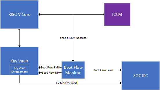 | ||
| 2731 | + | ||
| 2732 | +### Boot flow monitor | ||
| 2733 | + | ||
| 2734 | +The boot flow monitor detects firmware execution phase transitions by spying the ICCM memory interface. It compares bank-level read addresses against programmed FMC and RT region boundaries. | ||
| 2735 | + | ||
| 2736 | +#### ICCM region registers | ||
| 2737 | + | ||
| 2738 | +Four shadow-hardened registers define the FMC and RT code regions within ICCM address space: | ||
| 2739 | + | ||
| 2740 | +| Register | Address | Description | | ||
| 2741 | +| :------- | :------ | :---------- | | ||
| 2742 | +| INTERNAL_ICCM_FMC_START_ADDR | 0x30030650 | Start address of FMC region (18-bit ICCM-relative) | | ||
| 2743 | +| INTERNAL_ICCM_FMC_END_ADDR | 0x30030654 | End address of FMC region (inclusive) | | ||
| 2744 | +| INTERNAL_ICCM_RT_START_ADDR | 0x30030658 | Start address of RT region (18-bit ICCM-relative) | | ||
| 2745 | +| INTERNAL_ICCM_RT_END_ADDR | 0x3003065C | End address of RT region (inclusive) | | ||
| 2746 | +| INTERNAL_ICCM_REGION_LOCK | 0x30030660 | W1S lock -- once set, address registers cannot be modified until reset | | ||
| 2747 | + | ||
| 2748 | + | ||
| 2749 | +These registers use the `caliptra_prim_subreg_shadow` primitive for glitch hardening: | ||
| 2750 | +- **2-phase write protocol**: Each register must be written twice with the same value to commit. A single write updates only the shadow copy; the second matching write commits to the primary register. | ||
| 2751 | +- **Phase-clear-on-read**: A read operation resets the write phase to 0, preventing stale partial writes from persisting. | ||
| 2752 | +- **Error lockout**: If the shadow and committed copies diverge (storage fault), all further writes are blocked until reset. | ||
| 2753 | +- **Error reporting**: Storage faults assert `CPTRA_HW_ERROR_FATAL.shadow_storage_err[5]`. Phase-1/phase-0 mismatches assert `CPTRA_HW_ERROR_NON_FATAL.shadow_update_err[3]`. | ||
| 2754 | + | ||
| 2755 | +The effective lock for the boot flow monitor is `iccm_region_lock & iccm_all_shadows_committed` -- both the lock register must be set AND all four address registers must have completed their 2-phase writes. | ||
| 2756 | + | ||
| 2757 | +#### Transition detection | ||
| 2758 | + | ||
| 2759 | +The monitor uses MuBi4-encoded signals for glitch resistance: | ||
| 2760 | + | ||
| 2761 | +| Signal | Encoding | Meaning | | ||
| 2762 | +| :----- | :------- | :------ | | ||
| 2763 | +| `boot_flow_fmc` | MuBi4True/False | CPU has begun executing from the FMC region | | ||
| 2764 | +| `boot_flow_rt` | MuBi4True/False | CPU has begun executing from the RT region | | ||
| 2765 | +| `boot_flow_error` | MuBi4True/False | Fatal error detected in boot flow | | ||
| 2766 | + | ||
| 2767 | + | ||
| 2768 | +Transitions are one-way: once `boot_flow_fmc` becomes True, it remains True until reset. The monitor fires on the first ICCM read within the FMC region (after effective lock is set), and similarly for RT. | ||
| 2769 | + | ||
| 2770 | +#### Error conditions | ||
| 2771 | + | ||
| 2772 | +`boot_flow_error` is asserted (fatal) when any of the following occur: | ||
| 2773 | +- ICCM fetch while region lock is not set or shadow registers are not committed | ||
| 2774 | +- RT region fetch while `boot_flow_fmc` is False (illegal ROM->RT jump -- the RT transition is gated on FMC, so this fires the error without producing a transient `boot_flow_rt` pulse) | ||
| 2775 | +- ICCM fetch outside both the FMC and RT programmed regions after region lock is set (out-of-range execution) | ||
| 2776 | +- Any boot flow MuBi4 signal enters an invalid (non-True, non-False) encoding state | ||
| 2777 | + | ||
| 2778 | +#### Simulation support | ||
| 2779 | + | ||
| 2780 | +In simulation, `boot_flow_monitor_en` defaults to 0 (disabled). The testbench overrides this signal with a `force` when testing the feature. In hardware, the monitor is enabled when `debug_locked` is asserted AND `scan_mode` is deasserted. The monitor is disabled when debug is unlocked (to allow JTAG ICCM access and fake-ROM flows) and during scan mode (to prevent false transitions from clock-override activity on the ICCM banks). | ||
| 2781 | + | ||
| 2782 | +### KV monitor | ||
| 2783 | + | ||
| 2784 | +At each boot phase transition, the KV monitor validates that the expected DICE key slots are correctly populated. The monitor checks **only DICE derivation key slots** (0–9) — optional feature keys (Stable Owner Key, OCP Lock keys) are excluded from monitoring because they are conditionally derived and do not participate in the DICE trust chain. A mismatch triggers `kv_monitor_alert`, which escalates to `CPTRA_HW_ERROR_FATAL.kv_error[4]` and flushes all key entries. | ||
| 2785 | + | ||
| 2786 | +#### ROM->FMC checks (on `enter_fmc`) | ||
| 2787 | + | ||
| 2788 | +| Slot | Name | Expected dest_valid | | ||
| 2789 | +| :--- | :--- | :------------------ | | ||
| 2790 | +| 0 | SI_IDEV | AES_KEY | | ||
| 2791 | +| 1 | SI_LDEV | AES_KEY | | ||
| 2792 | +| 2 | KEY_LADDER | HMAC_KEY | | ||
| 2793 | +| 6 | FMC_CDI | HMAC_KEY | MLDSA_SEED | ECC_SEED | | ||
| 2794 | +| 7 | FMC_ECDSA | ECC_PKEY | | ||
| 2795 | +| 8 | FMC_MLDSA | MLDSA_SEED | | ||
| 2796 | + | ||
| 2797 | + | ||
| 2798 | +Additionally, per-slot crypto write counters verify **exact** expected derivation counts: | ||
| 2799 | +- Slot 6 (FMC_CDI): == 4 writes (IDevID CDI + LDevID intermediate + LDevID CDI + FMC Alias CDI) | ||
| 2800 | +- Slot 7 (FMC_ECDSA): == 2 writes (IDevID ECC keygen + FMC Alias ECC keygen) | ||
| 2801 | +- Slot 8 (FMC_MLDSA): == 2 writes (IDevID MLDSA keygen + FMC Alias MLDSA keygen) | ||
| 2802 | + | ||
| 2803 | +An exact match (rather than a minimum threshold) detects both truncated DICE chains (too few writes, indicating a skipped derivation step) and glitch-replayed operations (too many writes, which could overwrite the final safe key with an earlier intermediate value such as raw UDS). | ||
| 2804 | + | ||
| 2805 | +Write counters are 3-bit saturating counters that reset only on hard reset (`cptra_pwrgood`) or `flush_keyvault`, persisting across warm and FW update resets. Since ROM does not re-derive DICE keys on warm or FW update reset, the counters retain their cold-boot values and pass the exact-match check on subsequent transitions. | ||
| 2806 | + | ||
| 2807 | +#### FMC->RT checks (on `enter_rt`) | ||
| 2808 | + | ||
| 2809 | +| Slot | Name | Expected dest_valid | | ||
| 2810 | +| :--- | :--- | :------------------ | | ||
| 2811 | +| 4 | RT_CDI | HMAC_KEY | MLDSA_SEED | ECC_SEED | | ||
| 2812 | +| 5 | RT_ECDSA | ECC_PKEY | | ||
| 2813 | +| 9 | RT_MLDSA | MLDSA_SEED | | ||
| 2814 | + | ||
| 2815 | + | ||
| 2816 | +### KV enforcement | ||
| 2817 | + | ||
| 2818 | +Enforcement is applied continuously based on the current boot phase and atomically at transitions. | ||
| 2819 | + | ||
| 2820 | +#### Lock enforcement (continuous) | ||
| 2821 | + | ||
| 2822 | +| Condition | Slots affected | Action | | ||
| 2823 | +| :-------- | :------------- | :----- | | ||
| 2824 | +| `boot_flow_fmc` = True | 0, 1, 2, 6, 7, 8 | `lock_wr` asserted via hwset (HW-driven, cannot be cleared by SW) | | ||
| 2825 | +| `boot_flow_rt` = True | 4, 5, 9 | `lock_wr` asserted via hwset | | ||
| 2826 | +| `boot_flow_rt` = True | 6, 7, 8 | `lock_use` asserted via hwset (FMC keys cannot be used in RT) | | ||
| 2827 | + | ||
| 2828 | + | ||
| 2829 | +The `lock_wr` and `lock_use` fields have `hwset` property in the register definition, allowing hardware to set them without firmware intervention. Once set, they can only be cleared by `core_only_rst_b` de-assertion. | ||
| 2830 | + | ||
| 2831 | +#### Slot clearing (atomic, on transition edge) | ||
| 2832 | + | ||
| 2833 | +**DICE slots** — unconditionally cleared or preserved at each transition: | ||
| 2834 | + | ||
| 2835 | +| Slot | Purpose | ROM→FMC | FMC→RT | | ||
| 2836 | +| :--- | :------ | :------ | :----- | | ||
| 2837 | +| 0 | SI_IDEV | Preserved | Preserved | | ||
| 2838 | +| 1 | SI_LDEV | Preserved | Preserved | | ||
| 2839 | +| 2 | KEY_LADDER | Preserved | Preserved | | ||
| 2840 | +| 3 | TMP | Cleared | Cleared | | ||
| 2841 | +| 4 | RT_CDI | Cleared | Preserved | | ||
| 2842 | +| 5 | RT_ECDSA | Cleared | Preserved | | ||
| 2843 | +| 6 | FMC_CDI | Preserved | Preserved | | ||
| 2844 | +| 7 | FMC_ECDSA | Preserved | Preserved | | ||
| 2845 | +| 8 | FMC_MLDSA | Preserved | Preserved | | ||
| 2846 | +| 9 | RT_MLDSA | Cleared | Preserved | | ||
| 2847 | +| 10–14 | Unused | Cleared | Cleared | | ||
| 2848 | + | ||
| 2849 | + | ||
| 2850 | +**Conditionally-preserved slots** — behavior depends on active mode: | ||
| 2851 | + | ||
| 2852 | +| Slot | Purpose | Default (no optional features) | `stable_owner_key_en` | `ocp_lock_mode_en` | | ||
| 2853 | +| :--- | :------ | :----------------------------- | :-------------------- | :----------------- | | ||
| 2854 | +| 15 | Stable Owner Key | Cleared | Preserved | Cleared (mutually exclusive) | | ||
| 2855 | +| 16 | MDK | Cleared | Cleared | Preserved | | ||
| 2856 | +| 17–21 | Unused OCP range | Cleared | Cleared | Cleared | | ||
| 2857 | +| 22 | HEK seed | Cleared | Cleared | Preserved | | ||
| 2858 | +| 23 | MEK | Cleared | Cleared | **Always cleared** (DMA-accessible) | | ||
| 2859 | + | ||
| 2860 | + | ||
| 2861 | +Clearing destroys the key data and resets `dest_valid` and `last_dword` for the affected slots. | ||
| 2862 | + | ||
| 2863 | +#### Conditional slot preservation | ||
| 2864 | + | ||
| 2865 | +Two optional Caliptra features populate KV slots that must survive boot transitions when the feature is active, but must be cleared when inactive. These slots are **not monitored** (no dest_valid checks, no write counters) — the monitor is exclusively for DICE keys. Only the enforcement block (slot clearing) handles them conditionally. | ||
| 2866 | + | ||
| 2867 | +**Stable Owner Key (Slot 15)** | ||
| 2868 | + | ||
| 2869 | +The Stable Owner Root Key is conditionally derived by ROM when all three conditions are met: | ||
| 2870 | + | ||
| 2871 | +- `SUBSYSTEM_MODE_en` = 1 (Caliptra operating in subsystem mode) | ||
| 2872 | +- `OCP_LOCK_MODE_en` = 0 (OCP Lock feature is not active) | ||
| 2873 | +- `SS_STRAP_GENERIC[3][0]` = 1 (SoC strap enabling the stable owner key feature) | ||
| 2874 | + | ||
| 2875 | +The combined signal `stable_owner_key_en` is computed in `soc_ifc_top` and routed to the Key Vault. When active, slot 15 is excluded from `boot_flow_key_clear` at both ROM-to-FMC and FMC-to-RT transitions. When inactive, slot 15 is cleared normally. | ||
| 2876 | + | ||
| 2877 | +**OCP Lock Keys (Slots 16 and 22)** | ||
| 2878 | + | ||
| 2879 | +When OCP Lock mode is enabled (`ocp_lock_mode_en` = 1 from the `ss_ocp_lock_en` strap), DOE populates slot 16 (MDK) and slot 22 (HEK seed) before ROM runs. FMC and RT firmware require these keys for EPK, VEK, and MEK derivation in OCP Lock flows. | ||
| 2880 | + | ||
| 2881 | +When `ocp_lock_mode_en` is active, slots 16 and 22 are excluded from clearing at both transitions. When inactive, they are cleared normally. | ||
| 2882 | + | ||
| 2883 | +**Slot 23 (MEK) is always cleared** regardless of `ocp_lock_mode_en`. MEK has `DMA_DATA` in its `dest_valid` (it is DMA-accessible for key release), making it a security risk if it persists across transitions. RT firmware re-derives MEK when needed during OCP Lock key release flows. | ||
| 2884 | + | ||
| 2885 | +Only the specific slots that ROM or FMC actually derive (16 and 22) are preserved — not the entire OCP Lock range (16–23). Slots 17–21 and 23 are always cleared. | ||
| 2886 | + | ||
| 2887 | +**Mutual exclusion**: Stable Owner Key and OCP Lock are mutually exclusive by construction — `stable_owner_key_en` includes `~OCP_LOCK_MODE_en` in its definition. When OCP Lock is enabled, slot 15 is always cleared even if `SS_STRAP_GENERIC[3][0]` = 1. | ||
| 2888 | + | ||
| 2889 | +#### Error escalation | ||
| 2890 | + | ||
| 2891 | +Any of the following trigger all key entries to be flushed: | ||
| 2892 | +- `boot_flow_error` = MuBi4True | ||
| 2893 | +- `kv_monitor_alert` (dest_valid mismatch or write count violation) | ||
| 2894 | +- `kv_multi_write_err` (existing: multiple crypto engines writing simultaneously) | ||
| 2895 | + | ||
| 2896 | +The error is reported as `CPTRA_HW_ERROR_FATAL.kv_error[4]`, which is unmasked and always triggers an interrupt. | ||
| 2897 | + | ||
| 2898 | +### DOE lockdown | ||
| 2899 | + | ||
| 2900 | +Once the boot flow monitor detects that execution has transitioned to FMC or RT (i.e., `boot_flow_fmc` or `boot_flow_rt` is True), the DOE command register is forcibly cleared via `doe_cmd_lock`. This prevents any new de-obfuscation commands from being issued after the DICE key derivation phase is complete, closing the window for an attacker to re-derive secrets using the obfuscation key. | ||
| 2901 | + | ||
| 2902 | +### Error register summary | ||
| 2903 | + | ||
| 2904 | +| Register | Bit | Field | Trigger | | ||
| 2905 | +| :------- | :-- | :---- | :------ | | ||
| 2906 | +| CPTRA_HW_ERROR_FATAL | 4 | kv_error | Boot flow error OR KV monitor alert | | ||
| 2907 | +| CPTRA_HW_ERROR_FATAL | 5 | shadow_storage_err | ICCM region shadow register storage fault | | ||
| 2908 | +| CPTRA_HW_ERROR_NON_FATAL | 3 | shadow_update_err | ICCM region shadow register phase mismatch | | ||
| 2909 | + | ||
| 2910 | + | ||
| 2911 | +### DICE slot assignments | ||
| 2912 | + | ||
| 2913 | +The following table documents the key vault slot assignments used by the DICE key derivation chain (defined in `kv_defines_pkg.sv`): | ||
| 2914 | + | ||
| 2915 | +| Slot | Constant | Purpose | | ||
| 2916 | +| :--- | :------- | :------ | | ||
| 2917 | +| 0 | KV_SLOT_SI_IDEV | Silicon IDevID private key | | ||
| 2918 | +| 1 | KV_SLOT_SI_LDEV | Silicon LDevID private key | | ||
| 2919 | +| 2 | KV_SLOT_KEY_LADDER | Key ladder intermediate | | ||
| 2920 | +| 4 | KV_SLOT_RT_CDI | Runtime CDI | | ||
| 2921 | +| 5 | KV_SLOT_RT_ECDSA | Runtime ECDSA private key | | ||
| 2922 | +| 6 | KV_SLOT_FMC_CDI | FMC CDI (accumulates through DICE chain) | | ||
| 2923 | +| 7 | KV_SLOT_FMC_ECDSA | FMC ECDSA private key | | ||
| 2924 | +| 8 | KV_SLOT_FMC_MLDSA | FMC MLDSA private key | | ||
| 2925 | +| 9 | KV_SLOT_RT_MLDSA | Runtime MLDSA private key | | ||
| 2926 | + | ||
| 2927 | + | ||
| 2928 | +### Conditionally-preserved slot assignments | ||
| 2929 | + | ||
| 2930 | +The following slots are populated by optional features and conditionally preserved by enforcement (but not monitored): | ||
| 2931 | + | ||
| 2932 | +| Slot | Constant | Feature | Preserved when | | ||
| 2933 | +| :--- | :------- | :------ | :------------- | | ||
| 2934 | +| 15 | KV_SLOT_STABLE_OWNER | Stable Owner Root Key | `stable_owner_key_en` (subsystem mode, strap[3][0]=1, OCP Lock off) | | ||
| 2935 | +| 16 | OCP_LOCK_RT_OBF_KEY_KV_SLOT | MDK (runtime obfuscation key) | `ocp_lock_mode_en` | | ||
| 2936 | +| 22 | OCP_LOCK_HEK_SEED_KV_SLOT | HEK seed | `ocp_lock_mode_en` | | ||
| 2937 | +| 23 | OCP_LOCK_MEK_KV_SLOT | MEK (key release) | **Never** (always cleared — DMA-accessible, security risk) | | ||
| 2938 | + | ||
| 2939 | + | ||
| 2940 | +### ROM programming sequence | ||
| 2941 | + | ||
| 2942 | +ROM must perform the following steps before jumping to FMC: | ||
| 2943 | + | ||
| 2944 | +1. Complete all DICE key derivations (DOE decrypt, HMAC, ECC keygen, MLDSA keygen) | ||
| 2945 | +2. Program ICCM region registers with 2-phase writes: | ||
| 2946 | + - Write `INTERNAL_ICCM_FMC_START_ADDR` twice with the same value | ||
| 2947 | + - Write `INTERNAL_ICCM_FMC_END_ADDR` twice with the same value | ||
| 2948 | + - Write `INTERNAL_ICCM_RT_START_ADDR` twice with the same value | ||
| 2949 | + - Write `INTERNAL_ICCM_RT_END_ADDR` twice with the same value | ||
| 2950 | +3. Set `INTERNAL_ICCM_REGION_LOCK` (W1S) -- this arms the boot flow monitor | ||
| 2951 | +4. Jump to FMC entry point in ICCM | ||
| 2952 | + | ||
| 2953 | +The first instruction fetch from the FMC region triggers the ROM->FMC transition, at which point the KV monitor validates slot state and enforcement atomically applies locks and clears. | ||
| 2954 | + | ||
| 2955 | + | ||
| 2397 | 2956 | ## Data vault | |
| 2398 | 2957 | ||
| 2399 | 2958 | Data vault is a set of generic scratch pad registers with specific lock functionality and clearable on cold and warm resets. | |
| @@ -2403,6 +2962,117 @@ | |||
| 2403 | 2962 | * 4B scratchpad registers that are lockable but cleared on cold reset (8 registers) | |
| 2404 | 2963 | * 4B scratchpad registers that are lockable but cleared on warm reset (10 registers) | |
| 2405 | 2964 | * 4B scratchpad registers that are cleared on warm reset (8 registers) | |
| 2965 | + | ||
| 2966 | + | ||
| 2967 | +## OCP LOCK Hardware Architecture | ||
| 2968 | + | ||
| 2969 | +### Overview | ||
| 2970 | +The following hardware and ROM/FW enhancements support the OCP L.O.C.K. (a.k.a. **OCP LOCK**) flows defined for SSD applications. The specification is available here: | ||
| 2971 | +[OCP LOCK Spec](https://chipsalliance.github.io/Caliptra/ocp-lock/specification/HEAD) | ||
| 2972 | + | ||
| 2973 | +--- | ||
| 2974 | + | ||
| 2975 | +### Additional Registers, Straps, and Macros for OCP LOCK | ||
| 2976 | + | ||
| 2977 | +- **`SS_OCP_LOCK_CTRL.LOCK_IN_PROGRESS`** | ||
| 2978 | + A status/control bit used to enforce the new key Vvult (KV) rules required by OCP LOCK. Write-1-to-set, meaning that, once-enabled, OCP LOCK functionality will persist until the register is cleared by a cold reset. See the dedicated section below for details on the behaviors this register enables. | ||
| 2979 | + | ||
| 2980 | +- **`ss_ocp_lock_en`** (constant-value input strap) with a corresponding bit in **`CPTRA_HW_CONFIG`** register named **`OCP_LOCK_MODE_en`**: | ||
| 2981 | + - Enables Caliptra ROM to perform OCP LOCK operations (e.g., using DOE for HEK seed de-obfuscation, Key Release via AXI DMA). | ||
| 2982 | + - Allows the ROM to set `SS_OCP_LOCK_CTRL.LOCK_IN_PROGRESS`. | ||
| 2983 | + - `ss_ocp_lock_en` is a strap pin and **must be driven with a constant value by the integrator**. | ||
| 2984 | + - `CPTRA_HW_CONFIG` register samples this strap and store its value in `OCP_LOCK_MODE_en` bit | ||
| 2985 | + - This bit is only reflected in CPTRA_HW_CONFIG if CALIPTRA_MODE_SUBSYSTEM is defined | ||
| 2986 | + | ||
| 2987 | +- **HEK seed fuse register** | ||
| 2988 | + Holds the **obfuscated HEK seed**. ROM is responsible for performing the operation to de-obfuscate the HEK seed. | ||
| 2989 | + | ||
| 2990 | +- **Key release address and size straps** | ||
| 2991 | + Writable until `FUSE_WR_DONE`, then locked (same as fuses and other subsystem-mode straps). | ||
| 2992 | + - **Address strap** (`strap_ss_key_release_base_addr`): full destination address for key release; in OCP LOCK this is the destination for the MEK to be written. Firmware can derive the SFR base from this value as needed. | ||
| 2993 | + - **Size strap** (`strap_ss_key_release_key_size`): byte-count (dword-aligned count is required by HW) of the key to program to the destination address via the key release operation. Strap input values are forced to a dword value by hardware. If control firmware updates this value (prior to FUSE_WR_DONE being set), it must use a dword-aligned value. | ||
| 2994 | + | ||
| 2995 | +Refer to the [Caliptra Integration Spec](https://github.com/chipsalliance/caliptra-rtl/blob/main/docs/CaliptraIntegrationSpecification.md) for more details about macros and strap pins. | ||
| 2996 | + | ||
| 2997 | +--- | ||
| 2998 | + | ||
| 2999 | +### `SS_OCP_LOCK_CTRL.LOCK_IN_PROGRESS` Register Bit | ||
| 3000 | + | ||
| 3001 | +**When/How it is set** | ||
| 3002 | +- Set by **Caliptra ROM** after performing OCP LOCK-related derivations (HEK, MDK, etc.). | ||
| 3003 | +- Can be set **iff** (`ss_ocp_lock_en` is set to 1 **AND** `CALIPTRA_MODE_SUBSYSTEM` is defined). | ||
| 3004 | + - Once set, a value of 1 persists until the register is cleared by cold reset. | ||
| 3005 | + | ||
| 3006 | +**Enforcements/Effects** | ||
| 3007 | +- Reserves **key vault slots 0–15** for *standard* use-cases. | ||
| 3008 | +- Reserves **key vault slots 16–23** for *OCP LOCK* use-cases. | ||
| 3009 | + - Key Vault slot 16 (KV16) is reserved for holding the MDK | ||
| 3010 | + - Key Vault slot 23 (KV23) is reserved for holding the MEK | ||
| 3011 | +- Blocks interactions between *standard* slots and *LOCK* slots. This means that any crypto operation that uses a Key Vault input value (e.g. for Key, Block, Seed inputs) may not write the output to a Key Vault from a different region. E.g., When `SS_OCP_LOCK_CTRL.LOCK_IN_PROGRESS` is set, HMAC may not perform an operation that uses Key Vault slot 8 as BLOCK input and writes the output TAG to Key Vault slot 17. | ||
| 3012 | +- Enables **Key Release via AXI DMA**. | ||
| 3013 | +- Enables **AES engine to write output to Key Vault, which must use KV23**. | ||
| 3014 | + | ||
| 3015 | +> **Note:** If `SS_OCP_LOCK_CTRL.LOCK_IN_PROGRESS` is `1`, it also implies `ss_ocp_lock_en` and `CALIPTRA_MODE_SUBSYSTEM` are also `1`. | ||
| 3016 | + | ||
| 3017 | +--- | ||
| 3018 | + | ||
| 3019 | +### AES Write Path | ||
| 3020 | + | ||
| 3021 | +- **MEK** is the final OCP LOCK key. It is **decrypted and stored in KV23**. After decryption, MEK may be transferred to its destination (as specified by the input strap) **via AXI DMA**. | ||
| 3022 | +- OCP LOCK requires both the **AES write path** and a **DMA path** to the MEK destination. | ||
| 3023 | +- **Hardware enforcement:** MEK is written to **KV23**. Hardware recognizes the MEK generation request if there is an **AES-ECB decrypt** operation with **KV16 (MDK)** as the AES-ECB key and routes the result accordingly. In this case, output of the decrypted plaintext via the AES dataout register API is blocked. Any Key Vault write operation requested for the AES output that does not meet these requirements results in a Key Vault write failure status. | ||
| 3024 | + | ||
| 3025 | +--- | ||
| 3026 | + | ||
| 3027 | +### Key Vault Access Rules & Filtering (when `LOCK_IN_PROGRESS` is set) | ||
| 3028 | + | ||
| 3029 | +- **KV23 (MEK destination)**: **write-restricted to AES only**. | ||
| 3030 | +- **KV22 (HEK)**: **locked for writes until warm reset** (ROM requirement). | ||
| 3031 | +- **KV16 (MDK)**: **locked for writes until warm reset** (ROM requirement). | ||
| 3032 | +- If OCP LOCK mode is enabled: | ||
| 3033 | + - **KV23 must not be used** as input to other crypto operations—**only** as a **Key Release** source. | ||
| 3034 | + - **AES-ECB decrypt** with **key = KV16** **must** have **dest = KV23**; otherwise the destination is **FW**. | ||
| 3035 | + *Rationale:* Prevents malicious FW from writing known values into other KV slots via AES. | ||
| 3036 | +- **Additional KV behaviors** | ||
| 3037 | + - On write, hardware validates that the **destination** is legal for the **source/read**. If not valid, the Key Vault write operation returns a failing status. | ||
| 3038 | + - **No parallel crypto operations** permitted for cryptographic blocks with access to Key Vault. KV does not track this; Caliptra enforces this rule by evaluating each block's busy status indicator and signaling violations through the [CPTRA_HW_ERROR_FATAL](https://chipsalliance.github.io/caliptra-rtl/main/internal-regs/?p=clp.soc_ifc_reg.CPTRA_HW_ERROR_FATAL) register and corresponding interrupt at Caliptra top level design. | ||
| 3039 | + | ||
| 3040 | +--- | ||
| 3041 | + | ||
| 3042 | +### HEK Seed De‑obfuscation | ||
| 3043 | + | ||
| 3044 | +- Executed by **Caliptra ROM**. The DOE supports a HEK deobfuscation command that may be executed only once during a boot cycle. If Caliptra ROM does not run this flow to produce the HEK seed, it should run the flow with a dummy Key Vault slot to lock against future erroneous uses. | ||
| 3045 | +- **Hardware-supported HEK seed Deobfuscation Path:** Ratchet Fuse Register (**obfuscated HEK seed**) → **DOE** (with `OBF_KEY`) → **KV slot 22** (de-obfuscated seed). | ||
| 3046 | +- Caliptra ROM shall lock **KV22** for writes immediately it has derived the **HEK** into that slot. | ||
| 3047 | + | ||
| 3048 | +--- | ||
| 3049 | + | ||
| 3050 | +### Key Release | ||
| 3051 | + | ||
| 3052 | +Caliptra's AXI DMA supports a hardware path to write **KV23 (MEK)** to the SoC via the AXI manager interface. The following rules constrain this operation: | ||
| 3053 | +- Allowed **only** when `SS_OCP_LOCK_CTRL.LOCK_IN_PROGRESS` (sticky **W1SET**) is set by Caliptra ROM. | ||
| 3054 | +- Destination and size must match the values from the straps: | ||
| 3055 | + - `strap_ss_key_release_base_addr` | ||
| 3056 | + - `strap_ss_key_release_key_size` | ||
| 3057 | + | ||
| 3058 | +--- | ||
| 3059 | + | ||
| 3060 | +### Additional Security Hardening Specific to OCP LOCK Enhancements | ||
| 3061 | + | ||
| 3062 | +**Scan/Debug Protections** | ||
| 3063 | +- Flush **DMA FIFOs** to prevent leakage of secrets via scan chain. | ||
| 3064 | +- Flush **AES ↔ KV** interface. | ||
| 3065 | + | ||
| 3066 | +**AES/KV/DMA Robustness** | ||
| 3067 | +- **AES → KV write path:** The key can't be written to key vault unless key_size bytes are decrypted by AES. | ||
| 3068 | +- Validate **DMA `key_size`**; **error** if `key_size > 512b`. | ||
| 3069 | +- Avoid hangs when **`key_size` != KV read DWORD count**: | ||
| 3070 | + - On KV reads, if `key_size` is **smaller** than the KV entry, **drop extra data** (do not push to FIFO). | ||
| 3071 | +- **DMA KV read error**: Raised on the **first transfer cycle** from KV to DMA; DMA transitions immediately to **`DMA_ERROR`** without issuing an AXI transfer. | ||
| 3072 | +- **KV write enable sourced from AES** (during OCP LOCK) so it **cannot** be modified mid-transfer. | ||
| 3073 | +- **Enable AES ↔ KV write path** only if `SS_OCP_LOCK_CTRL.LOCK_IN_PROGRESS` is set. | ||
| 3074 | + | ||
| 3075 | + | ||
| 2406 | 3076 | ||
| 2407 | 3077 | ## Cryptographic blocks fatal and non-fatal errors | |
| 2408 | 3078 | ||
| @@ -2485,10 +3155,11 @@ | |||
| 2485 | 3155 | 9. Coron, J.-S.: Resistance against differential power analysis for elliptic curve cryptosystems. In: Ko¸c, C¸ .K., Paar, C. (eds.) CHES 1999. LNCS, vol. 1717, pp. 292–302. | |
| 2486 | 3156 | 10. Schindler, W., Wiemers, A.: Efficient side-channel attacks on scalar blinding on elliptic curves with special structure. In: NISTWorkshop on ECC Standards (2015). | |
| 2487 | 3157 | 11. National Institute of Standards and Technology, "Digital Signature Standard (DSS)", Federal Information Processing Standards Publication (FIPS PUB) 186-4, July 2013. | |
| 2488 | -12. NIST SP 800-90A, Rev 1: "Recommendation for Random Number Generation Using Deterministic Random Bit Generators", 2012. | | ||
| 3158 | +12. NIST SP 800-90A, Rev 1: "Recommendation for Random Number Generation Using Deterministic Random Bit Generators", 2012. | ||
| 2489 | 3159 | 13. CHIPS Alliance, “RISC-V VeeR EL2 Programmer’s Reference Manual” \[Online\] Available at https://github.com/chipsalliance/Cores-VeeR-EL2/blob/main/docs/RISC-V_VeeR_EL2_PRM.pdf. | |
| 2490 | 3160 | 14. “The RISC-V Instruction Set Manual, Volume I: User-Level ISA, Document Version 20191213”, Editors Andrew Waterman and Krste Asanovi ́c, RISC-V Foundation, December 2019. Available at https://riscv.org/technical/specifications/. | |
| 2491 | 3161 | 15. “The RISC-V Instruction Set Manual, Volume II: Privileged Architecture, Document Version 20211203”, Editors Andrew Waterman, Krste Asanovi ́c, and John Hauser, RISC-V International, December 2021. Available at https://riscv.org/technical/specifications/. | |
| 2492 | -16. NIST SP 800-56A, Rev 3: "Recommendation for Pair-Wise Key-Establishment Schemes Using Discrete Logarithm Cryptography", 2018, | | ||
| 3162 | +16. NIST SP 800-56A, Rev 3: "Recommendation for Pair-Wise Key-Establishment Schemes Using Discrete Logarithm Cryptography", 2018. | ||
| 3163 | +17. NIST FIPS 202: "SHA-3 Standard: Permutation-Based Hash and Extendable-Output Functions", 2015. Available at: [https://csrc.nist.gov/pubs/fips/202/final](https://doi.org/10.6028/NIST.FIPS.202). | ||
| 2493 | 3164 | ||
| 2494 | 3165 | <sup>[1]</sup> _Caliptra.** **Spanish for “root cap” and describes the deepest part of the root_ | |
Image not present in this version
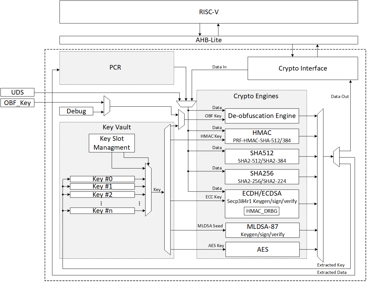
Image not present in this version
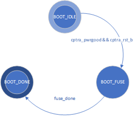
Image not present in this version
Image not present in this version

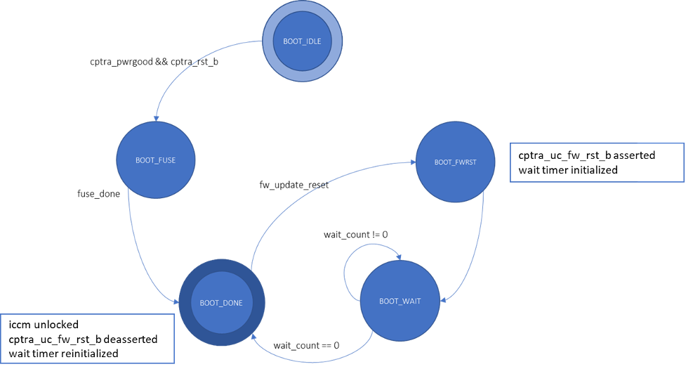
Image not present in this version