v1.2: Caliptra_CDC_JTAG_code_snippet.png
v2.0: Caliptra_CDC_JTAG_code_snippet.png
Image not present in this version
| @@ -1,12 +1,12 @@ | |||
| 1 | 1 | <div style="font-size: 0.85em; color: #656d76; margin-bottom: 1em; padding: 0.5em; background: #f6f8fa; border-radius: 4px;"> | |
| 2 | -📄 Source: <a href="https://github.com/chipsalliance/caliptra-rtl/blob/5f85fb4bc95b753a2f7d042db7dc2644ca1e8c49/docs/CaliptraIntegrationSpecification.md" target="_blank">chipsalliance/caliptra-rtl/docs/CaliptraIntegrationSpecification.md</a> @ <code>5f85fb4</code> | ||
| 2 | +📄 Source: <a href="https://github.com/chipsalliance/caliptra-rtl/blob/35b0bc5691b2bd0fc180403914cfabe207379089/docs/CaliptraIntegrationSpecification.md" target="_blank">chipsalliance/caliptra-rtl/docs/CaliptraIntegrationSpecification.md</a> @ <code>35b0bc5</code> | ||
| 3 | 3 | </div> | |
| 4 | 4 | ||
| 5 | 5 |  | |
| 6 | 6 | ||
| 7 | 7 | <p style="text-align: center;">Caliptra Integration Specification</p> | |
| 8 | 8 | ||
| 9 | -<p style="text-align: center;">Version 1.1</p> | ||
| 9 | +<p style="text-align: center;">Version 2.0.3</p> | ||
| 10 | 10 | ||
| 11 | 11 | <div style="page-break-after: always"></div> | |
| 12 | 12 | ||
| @@ -57,24 +57,26 @@ | |||
| 57 | 57 | ||
| 58 | 58 | | **Parameter name** | **Width** | **Defines file** | **Description** | | |
| 59 | 59 | | :--------- | :--------- | :--------- | :--------- | | |
| 60 | -| CPTRA_SET_MBOX_PAUSER_INTEG | 5 | soc_ifc_pkg.sv | Each bit hardcodes the valid PAUSER for mailbox at integration time. | | ||
| 61 | -| CPTRA_MBOX_VALID_PAUSER | \[4:0\]\[31:0\] | soc_ifc_pkg.sv | Each parameter corresponds to a hardcoded valid PAUSER value for mailbox, set at integration time. Must set corresponding bit in the CPTRA_SET_MBOX_PAUSER_INTEG parameter for this valid pauser override to be used. | | ||
| 62 | -| CPTRA_DEF_MBOX_VALID_PAUSER | 32 | soc_ifc_pkg.sv | Sets the default valid PAUSER for mailbox accesses. This PAUSER is valid at all times. | | ||
| 63 | -| CPTRA_SET_FUSE_PAUSER_INTEG | 1 | soc_ifc_pkg.sv | Sets the valid PAUSER for fuse accesses at integration time. | | ||
| 64 | -| CPTRA_FUSE_VALID_PAUSER | 32 | soc_ifc_pkg.sv | Overrides the programmable valid PAUSER for fuse accesses when CPTRA_SET_FUSE_PAUSER_INTEG is set to 1. | | ||
| 60 | +| CPTRA_SET_MBOX_AXI_USER_INTEG | 5 | soc_ifc_pkg.sv | Each bit hardcodes the valid AXI_USER for mailbox at integration time. | | ||
| 61 | +| CPTRA_MBOX_VALID_AXI_USER | \[4:0\]\[31:0\] | soc_ifc_pkg.sv | Each parameter corresponds to a hardcoded valid AXI_USER value for mailbox, set at integration time. Must set corresponding bit in the CPTRA_SET_MBOX_AXI_USER_INTEG parameter for this valid axi user override to be used. CANNOT use value 0xFFFFFFFF. This is reserved for Caliptra-internal usage. | | ||
| 62 | +| CPTRA_DEF_MBOX_VALID_AXI_USER | 32 | soc_ifc_pkg.sv | Sets the default valid AXI_USER for mailbox accesses. This AXI_USER is valid at all times. CANNOT use value 0xFFFFFFFF. This is reserved for Caliptra-internal usage. | | ||
| 63 | +| CPTRA_SET_FUSE_AXI_USER_INTEG | 1 | soc_ifc_pkg.sv | Sets the valid AXI_USER for fuse accesses at integration time. | | ||
| 64 | +| CPTRA_FUSE_VALID_AXI_USER | 32 | soc_ifc_pkg.sv | Overrides the programmable valid AXI_USER for fuse accesses when CPTRA_SET_FUSE_AXI_USER_INTEG is set to 1. CANNOT use value 0xFFFFFFFF. This is reserved for Caliptra-internal usage. | | ||
| 65 | 65 | ||
| 66 | 66 | ||
| 67 | 67 | *Table 3: Integration Defines* | |
| 68 | 68 | ||
| 69 | 69 | | **Defines** | **Defines file** | **Description** | | |
| 70 | 70 | | :--------- | :--------- | :--------- | | |
| 71 | -| CALIPTRA_INTERNAL_TRNG | config_defines.svh | Defining this enables the internal TRNG source. | | ||
| 72 | -| CALIPTRA_INTERNAL_UART | config_defines.svh | Defining this enables the internal UART. | | ||
| 73 | -| CALIPTRA_INTERNAL_QSPI | config_defines.svh | Defining this enables the internal QSPI. | | ||
| 71 | +| CALIPTRA_INTERNAL_TRNG | config_defines.svh | Defining this enables the internal TRNG source. This must be set to 1 in Subsystem mode. | | ||
| 72 | +| CALIPTRA_MODE_SUBSYSTEM | config_defines.svh | Defining this enables Caliptra to operate in Subsystem mode. This includes features such as the debug unlock flow, AXI DMA (for recovery flow), Subsystem-level straps, among other capabilites. See [Caliptra Subsystem Architectural Flows](https://github.com/chipsalliance/Caliptra/blob/main/doc/Caliptra.md#caliptra-subsystem-architectural-flows) for more details | | ||
| 74 | 73 | | USER_ICG | config_defines.svh | If added by an integrator, provides the name of the custom clock gating module that is used in [clk_gate.sv](../src/libs/rtl/clk_gate.sv). USER_ICG replaces the clock gating module, CALIPTRA_ICG, defined in [caliptra_icg.sv](../src/libs/rtl/caliptra_icg.sv). This substitution is only performed if integrators also define TECH_SPECIFIC_ICG. | | |
| 75 | 74 | | TECH_SPECIFIC_ICG | config_defines.svh | Defining this causes the custom, integrator-defined clock gate module (indicated by the USER_ICG macro) to be used in place of the native Caliptra clock gate module. | | |
| 76 | 75 | | USER_EC_RV_ICG | config_defines.svh | If added by an integrator, provides the name of the custom clock gating module that is used in the RISC-V core. USER_EC_RV_ICG replaces the clock gating module, TEC_RV_ICG, defined in [beh_lib.sv](../src/riscv_core/veer_el2/rtl/lib/beh_lib.sv). This substitution is only performed if integrators also define TECH_SPECIFIC_EC_RV_ICG. | | |
| 77 | 76 | | TECH_SPECIFIC_EC_RV_ICG | config_defines.svh | Defining this causes the custom, integrator-defined clock gate module (indicated by the USER_EC_RV_ICG macro) to be used in place of the native RISC-V core clock gate module. | | |
| 77 | +| CALIPTRA_AXI_DMA_ADDR_WIDTH | config_defines.svh | Defines the address width for the Caliptra AXI Manager interface, driven by Caliptra's DMA assist block. The address width value assigned to this macro should match the address width that is expected at the integrator's SoC AXI interconnect. | | ||
| 78 | +| CALIPTRA_PRIM_ROOT | environment variable | The integrator needs to set this environment variable to the path to technology specific modules for synthesis. Defaults to $CALIPTRA_ROOT/src/caliptra_prim_generic. | | ||
| 79 | +| CALIPTRA_PRIM_MODULE_PREFIX | environment variable | The integrator needs to set this environment variable to specify the module name prefix for technology specific modules for synthesus. Defaults to 'caliptra_prim_generic'. | | ||
| 78 | 80 | ||
| 79 | 81 | ||
| 80 | 82 | ## Interface | |
| @@ -90,45 +92,60 @@ | |||
| 90 | 92 | | clk | 1 | Input || Convergence and validation done at 400MHz. All other frequencies are up to the user. | | |
| 91 | 93 | ||
| 92 | 94 | ||
| 93 | -*Table 5: APB Interface* | ||
| 95 | +*Table 5: AXI Subordinate Interface* | ||
| 94 | 96 | ||
| 95 | 97 | | Signal name | Width | Driver | Synchronous (as viewed from Caliptra’s boundary) | Description | | |
| 96 | 98 | | :--------- | :--------- | :--------- | :--------- | :--------- | | |
| 97 | -| PADDR | CALIPTRA_APB_ADDR_WIDTH | Input | Synchronous to clk | Address bus | | ||
| 98 | -| PPROT | 3 | Input | Synchronous to clk | Protection level | | ||
| 99 | -| PSEL | 1 | Input | Synchronous to clk | Select line | | ||
| 100 | -| PENABLE | 1 | Input | Synchronous to clk | Indicates the second and subsequent cycles. | | ||
| 101 | -| PWRITE | 1 | Input | Synchronous to clk | Indicates transfer is a write when high or a read when low. | | ||
| 102 | -| PWDATA | CALIPTRA_APB_DATA_WIDTH | Input | Synchronous to clk | Write data bus | | ||
| 103 | -| PAUSER | CALIPTRA_APB_USER_WIDTH | Input | Synchronous to clk | Sideband signal indicating requestor ID for transfer. | | ||
| 104 | -| PREADY | 1 | Output | Synchronous to clk | Used to extend an APB transfer by completer. | | ||
| 105 | -| PRDATA | CALIPTRA_APB_DATA_WIDTH | Output | Synchronous to clk | Read data bus | | ||
| 106 | -| PSLVERR | 1 | Output | Synchronous to clk | Transfer error | | ||
| 107 | - | ||
| 108 | - | ||
| 109 | -*Table 6: QSPI signals* | ||
| 110 | - | ||
| 111 | -| Signal name | Width | Driver | Synchronous (as viewed from Caliptra’s boundary) | Description | | ||
| 112 | -| :--------- | :--------- | :--------- | :--------- | :--------- | | ||
| 113 | -| qspi_clk_o | 1 | Output || QSPI clock | | ||
| 114 | -| qspi_cs_no | 2 | Output | Synchronous to qspi_clk_o | QSPI chip select | | ||
| 115 | -| qspi_d_i | 4 | Input | Synchronous to qspi_clk_o | QSPI data lanes for receiving data. | | ||
| 116 | -| qspi_d_o | 4 | Output | Synchronous to qspi_clk_o | QSPI data output lanes for sending opcode and address. | | ||
| 117 | -| qspi_d_en_o | 4 | Output | Synchronous to qspi_clk_o | QSPI enable pins to control data direction. | | ||
| 118 | - | ||
| 119 | - | ||
| 120 | -*Table 7: Mailbox notifications* | ||
| 99 | +| araddr | AW | Input | Synchronous to clk | AR channel address | | ||
| 100 | +| arburst | 2 | Input | Synchronous to clk | AR channel burst encoding | | ||
| 101 | +| arsize | 3 | Input | Synchronous to clk | AR channel size encoding | | ||
| 102 | +| arlen | 8 | Input | Synchronous to clk | AR channel length, beats in the burst | | ||
| 103 | +| aruser | UW | Input | Synchronous to clk | AR channel user signal. Identifies the requester for mailbox and fuse access. See AXI_USER details for more information. | | ||
| 104 | +| arid | IW | Input | Synchronous to clk | AR channel id signal | | ||
| 105 | +| arlock | 1 | Input | Synchronous to clk | AR channel lock signal | | ||
| 106 | +| arvalid | 1 | Input | Synchronous to clk | AR channel valid handshake signal | | ||
| 107 | +| arready | 1 | Output | Synchronous to clk | AR channel ready handshake signal | | ||
| 108 | +| rdata | DW | Output | Synchronous to clk | R channel read response data | | ||
| 109 | +| rresp | 2 | Output | Synchronous to clk | R channel read response encoding | | ||
| 110 | +| rid | IW | Output | Synchronous to clk | R channel read response id signal | | ||
| 111 | +| ruser | UW | Output | Synchronous to clk | R channel read response user signal | | ||
| 112 | +| rlast | 1 | Output | Synchronous to clk | R channel read response last beat signal | | ||
| 113 | +| rvalid | 1 | Output | Synchronous to clk | R channel valid handhsake signal | | ||
| 114 | +| rready | 1 | Input | Synchronous to clk | R channel ready handshake signal | | ||
| 115 | +| awaddr | AW | Input | Synchronous to clk | AW channel address | | ||
| 116 | +| awburst | 2 | Input | Synchronous to clk | AW channel burst encoding | | ||
| 117 | +| awsize | 3 | Input | Synchronous to clk | AW channel size encoding | | ||
| 118 | +| awlen | 8 | Input | Synchronous to clk | AW channel length, beats in the burst | | ||
| 119 | +| awuser | UW | Input | Synchronous to clk | AW channel user signal. Identifies the requester for mailbox and fuse access. See AXI_USER details for more information. | | ||
| 120 | +| awid | IW | Input | Synchronous to clk | AW channel id signal | | ||
| 121 | +| awlock | 1 | Input | Synchronous to clk | AW channel lock signal | | ||
| 122 | +| awvalid | 1 | Input | Synchronous to clk | AW channel valid handhsake signal | | ||
| 123 | +| awready | 1 | Output | Synchronous to clk | AW channel ready handshake signal | | ||
| 124 | +| wdata | DW | Input | Synchronous to clk | W channel write data | | ||
| 125 | +| wuser | UW | Input | Synchronous to clk | W channel write user | | ||
| 126 | +| wstrb | DW/8 | Input | Synchronous to clk | W channel write strobe. Byte enable. | | ||
| 127 | +| wlast | 1 | Input | Synchronous to clk | W channel write last beat signal | | ||
| 128 | +| wvalid | 1 | Input | Synchronous to clk | W channel valid handhsake signal | | ||
| 129 | +| wready | 1 | Output | Synchronous to clk | W channel ready handshake signal | | ||
| 130 | +| bresp | 2 | Output | Synchronous to clk | B channel write response encoding | | ||
| 131 | +| bid | IW | Output | Synchronous to clk | B channel write response id signal | | ||
| 132 | +| buser | UW | Output | Synchronous to clk | B channel write response user signal | | ||
| 133 | +| bvalid | 1 | Output | Synchronous to clk | B channel valid handhsake signal | | ||
| 134 | +| bready | 1 | Input | Synchronous to clk | B channel ready handshake signal | | ||
| 135 | + | ||
| 136 | + | ||
| 137 | +*Table 6: Mailbox notifications* | ||
| 121 | 138 | ||
| 122 | 139 | | Signal name | Width | Driver | Synchronous (as viewed from Caliptra’s boundary) | Description | | |
| 123 | 140 | | :--------- | :--------- | :--------- | :--------- | :--------- | | |
| 124 | 141 | | ready_for_fuses | 1 | Output | Synchronous to clk | Indicates that Caliptra is ready for fuse programming. | | |
| 125 | -| ready_for_fw_push | 1 | Output | Synchronous to clk | Indicates that Caliptra is ready for firmware. | | ||
| 142 | +| ready_for_mb_processing | 1 | Output | Synchronous to clk | Indicates that Caliptra is ready for processing mailbox commands. | | ||
| 126 | 143 | | ready_for_runtime | 1 | Output | Synchronous to clk | Indicates that Caliptra firmware is ready for RT flow. | | |
| 127 | -| mailbox_data_avail | 1 | Output | Synchronous to clk | Indicates that the mailbox has data for SoC to read (reflects the value of the register). | | ||
| 128 | -| mailbox_flow_done | 1 | Output | Synchronous to clk | Indicates that the mailbox flow is complete (reflects the value of the register). | | ||
| 129 | - | ||
| 130 | - | ||
| 131 | -*Table 8: SRAM interface* | ||
| 144 | +| mailbox_data_avail | 1 | Output | Synchronous to clk | Indicates that the mailbox has a response for SoC to read. Signal is set when the mailbox transitions to the EXECUTE_SOC state, which is also reported in the `mbox_status` register. | | ||
| 145 | +| mailbox_flow_done | 1 | Output | Synchronous to clk | Deprecated output signal. Reflects the value from the CPTRA_FLOW_STATUS register field `mailbox_flow_done`, which is not used by firmware. For an indicator that Caliptra has completed its processing of the mailbox flow, an SoC may use the `mailbox_data_avail` signal. | | ||
| 146 | + | ||
| 147 | + | ||
| 148 | +*Table 7: Caliptra SRAM interface* | ||
| 132 | 149 | ||
| 133 | 150 | | Signal name | Width | Driver | Synchronous (as viewed from Caliptra’s boundary) | Description | | |
| 134 | 151 | | :--------- | :--------- | :--------- | :--------- | :--------- | | |
| @@ -143,49 +160,111 @@ | |||
| 143 | 160 | | iccm_clken | ICCM_NUM_BANKS | Input | Synchronous to clk | Per-bank clock enable | | |
| 144 | 161 | | iccm_wren_bank | ICCM_NUM_BANKS | Input | Synchronous to clk | Per-bank write enable | | |
| 145 | 162 | | iccm_addr_bank | ICCM_NUM_BANKS x (ICCM_BITS-4) | Input | Synchronous to clk | Per-bank address | | |
| 146 | -| iccm_bank_wr_data | ICCM_NUM_BANKS x 39 | Input | Synchronous to clk | Per-bank input data | | ||
| 147 | -| iccm_bank_dout | ICCM_NUM_BANKS x 39 | Output | Synchronous to clk | Per-bank output data | | ||
| 163 | +| iccm_bank_wr_data | ICCM_NUM_BANKS x 32 | Input | Synchronous to clk | Per-bank input data | | ||
| 164 | +| iccm_bank_wr_ecc | ICCM_NUM_BANKS x 7 | Input | Synchronous to clk | Per-bank input ecc | | ||
| 165 | +| iccm_bank_dout | ICCM_NUM_BANKS x 32 | Output | Synchronous to clk | Per-bank output data | | ||
| 166 | +| iccm_bank_ecc | ICCM_NUM_BANKS x 7 | Output | Synchronous to clk | Per-bank output ecc | | ||
| 148 | 167 | | dccm_clken | DCCM_NUM_BANKS | Input | Synchronous to clk | Per-bank clock enable | | |
| 149 | 168 | | dccm_wren_bank | DCCM_NUM_BANKS | Input | Synchronous to clk | Per-bank write enable | | |
| 150 | 169 | | dccm_addr_bank | DCCM_NUM_BANKS x (DCCM_BITS-4) | Input | Synchronous to clk | Per-bank address | | |
| 151 | -| dccm_wr_data_bank | DCCM_NUM_BANKS x DCCM_FDATA_WIDTH | Input | Synchronous to clk | Per-bank input data | | ||
| 152 | -| dccm_bank_dout | DCCM_NUM_BANKS x DCCM_FDATA_WIDTH | Output | Synchronous to clk | Per-bank output data | | ||
| 170 | +| dccm_wr_data_bank | DCCM_NUM_BANKS x DCCM_DATA_WIDTH | Input | Synchronous to clk | Per-bank input data | | ||
| 171 | +| dccm_wr_ecc_bank | DCCM_NUM_BANKS x DCCM_ECC_WIDTH | Input | Synchronous to clk | Per-bank input ecc | | ||
| 172 | +| dccm_bank_dout | DCCM_NUM_BANKS x DCCM_DATA_WIDTH | Output | Synchronous to clk | Per-bank output data | | ||
| 173 | +| dccm_bank_ecc | DCCM_NUM_BANKS x DCCM_ECC_WIDTH | Output | Synchronous to clk | Per-bank output ecc | | ||
| 174 | + | ||
| 175 | + | ||
| 176 | +*Table 8: Adams-Bridge SRAM Interface* | ||
| 177 | + | ||
| 178 | +Adams-Bridge SRAM interface is used to connect the necessary SRAM instances for Adams-Bridge. | ||
| 179 | +There are 8 SRAMs, 2 of which have 2 banks. Each SRAM has a parameterized data width and depth used to calculate the addr width. | ||
| 180 | + | ||
| 181 | +All memories are modeled as 1 read 1 write port RAMs with a flopped read data. | ||
| 182 | +See abr_1r1w_ram.sv and abr_1r1w_be_ram.sv for examples. | ||
| 183 | +Strobe width describes the number of bits enabled by each strobe. All strobed memories are byte enabled in the design. | ||
| 184 | +See [ABR Memory requirement](https://github.com/chipsalliance/adams-bridge/blob/main/docs/AdamsBridgeHardwareSpecification.md#memory-requirement) for more details. | ||
| 185 | + | ||
| 186 | +The full set of wires is encapsulated in the mldsa_mem_if construct mldsa_memory_export at the Caliptra boundary. | ||
| 187 | + | ||
| 188 | +The table below details the interface required for each SRAM. Driver direction is from the perspective of Caliptra. | ||
| 189 | + | ||
| 190 | +| Signal name | Width | Driver | Synchronous (as viewed from Caliptra’s boundary) | Description | | ||
| 191 | +| :---------- | :--------- | :--------- | :--------- | :--------- | | ||
| 192 | +| we_i | 1 | Output | Synchronous to clk | Write enable | | ||
| 193 | +| waddr_i | ADDR_W | Output | Synchronous to clk | Write address | | ||
| 194 | +| wdata_i | DATA_W | Output | Synchronous to clk | Write data | | ||
| 195 | +| wstrobe_i | DATA_W/8 | Output | Synchronous to clk | Write strobe (only for sig_z and pk memories) | | ||
| 196 | +| re_i | 1 | Output | Synchronous to clk | Read enable | | ||
| 197 | +| raddr_i | ADDR_W | Output | Synchronous to clk | Read address | | ||
| 198 | +| rdata_o | DATA_W | Input | Synchronous to clk | Read data | | ||
| 153 | 199 | ||
| 154 | 200 | ||
| 155 | 201 | *Table 9: JTAG interface* | |
| 156 | 202 | ||
| 157 | 203 | | Signal name | Width | Driver | Synchronous (as viewed from Caliptra’s boundary) | Description | | |
| 158 | 204 | | :--------- | :--------- | :--------- | :--------- | :--------- | | |
| 159 | -| jtag_tck | 1 | input ||| | ||
| 160 | -| jtag_tms | 1 | input | Synchronous to jtag_tck || | ||
| 161 | -| jtag_tdi | 1 | input | Synchronous to jtag_tck || | ||
| 162 | -| jtag_trst_n | 1 | input | Asynchronous assertion<br>Synchronous deassertion to jtag_tck || | ||
| 163 | -| jtag_tdo | 1 | output | Synchronous to jtag_tck || | ||
| 164 | - | ||
| 165 | - | ||
| 166 | -*Table 10: UART interface* | ||
| 167 | - | ||
| 205 | +| jtag_tck | 1 | Input ||| | ||
| 206 | +| jtag_tms | 1 | Input | Synchronous to jtag_tck || | ||
| 207 | +| jtag_tdi | 1 | Input | Synchronous to jtag_tck || | ||
| 208 | +| jtag_trst_n | 1 | Input | Asynchronous assertion<br>Synchronous deassertion to jtag_tck || | ||
| 209 | +| jtag_tdo | 1 | Output | Synchronous to jtag_tck || | ||
| 210 | + | ||
| 211 | + | ||
| 212 | +*Table 10: RISC-V Trace interface* | ||
| 168 | 213 | | Signal name | Width | Driver | Synchronous (as viewed from Caliptra’s boundary) | Description | | |
| 169 | 214 | | :--------- | :--------- | :--------- | :--------- | :--------- | | |
| 170 | -| uart_tx | 1 | output || UART transmit pin | | ||
| 171 | -| uart_rx | 1 | input || UART receive pin | | ||
| 172 | - | ||
| 173 | - | ||
| 174 | -*Table 11: Security and miscellaneous* | ||
| 215 | +| trace_rv_i_insn_ip | 32 | Output | Synchronous to clk | Trace signals from Caliptra RV core instance. Refer to VeeR documentation for more details. | | ||
| 216 | +| trace_rv_i_address_ip | 32 | Output | Synchronous to clk | Trace signals from Caliptra RV core instance. Refer to VeeR documentation for more details. | | ||
| 217 | +| trace_rv_i_valid_ip | 1 | Output | Synchronous to clk | Trace signals from Caliptra RV core instance. Refer to VeeR documentation for more details. | | ||
| 218 | +| trace_rv_i_exception_ip | 1 | Output | Synchronous to clk | Trace signals from Caliptra RV core instance. Refer to VeeR documentation for more details. | | ||
| 219 | +| trace_rv_i_ecause_ip | 5 | Output | Synchronous to clk | Trace signals from Caliptra RV core instance. Refer to VeeR documentation for more details. | | ||
| 220 | +| trace_rv_i_interrupt_ip | 1 | Output | Synchronous to clk | Trace signals from Caliptra RV core instance. Refer to VeeR documentation for more details. | | ||
| 221 | +| trace_rv_i_tval_ip | 32 | Output | Synchronous to clk | Trace signals from Caliptra RV core instance. Refer to VeeR documentation for more details. | | ||
| 222 | + | ||
| 223 | + | ||
| 224 | +*Table 11: Subsystem Straps and Control* | ||
| 225 | + | ||
| 226 | +| Signal name | Width | Driver | Synchronous (as viewed from Caliptra’s boundary) | Description | | ||
| 227 | +| :---------- | :--------- | :--------- | :----------------------------------------------- | :--------- | | ||
| 228 | +| strap_ss_caliptra_base_addr | 64 | Input Strap | Synchronous to clk | Used in Subsystem mode only. In Passive mode, integrators shall tie this input to 0. | | ||
| 229 | +| strap_ss_mci_base_addr | 64 | Input Strap | Synchronous to clk | Used in Subsystem mode only. In Passive mode, integrators shall tie this input to 0. | | ||
| 230 | +| strap_ss_recovery_ifc_base_addr | 64 | Input Strap | Synchronous to clk | Used in Subsystem mode only. In Passive mode, integrators shall tie this input to 0. | | ||
| 231 | +| strap_ss_otp_fc_base_addr | 64 | Input Strap | Synchronous to clk | Used in Subsystem mode only. In Passive mode, integrators shall tie this input to 0. | | ||
| 232 | +| strap_ss_uds_seed_base_addr | 64 | Input Strap | Synchronous to clk | Used in Subsystem mode only. In Passive mode, integrators shall tie this input to 0. | | ||
| 233 | +| strap_ss_prod_debug_unlock_auth_pk_hash_reg_bank_offset | 32 | Input Strap | Synchronous to clk | Used in Subsystem mode only. In Passive mode, integrators shall tie this input to 0. | | ||
| 234 | +| strap_ss_num_of_prod_debug_unlock_auth_pk_hashes | 32 | Input Strap | Synchronous to clk | Used in Subsystem mode only. In Passive mode, integrators shall tie this input to 0. | | ||
| 235 | +| strap_ss_caliptra_dma_axi_user | 32 | Input Strap | Synchronous to clk | Used in Subsystem mode only. In Passive mode, integrators shall tie this input to 0. | | ||
| 236 | +| strap_ss_strap_generic_0 | 32 | Input Strap | Synchronous to clk | Used in Subsystem mode only. In Passive mode, integrators shall tie this input to 0. | | ||
| 237 | +| strap_ss_strap_generic_1 | 32 | Input Strap | Synchronous to clk | Used in Subsystem mode only. In Passive mode, integrators shall tie this input to 0. | | ||
| 238 | +| strap_ss_strap_generic_2 | 32 | Input Strap | Synchronous to clk | Used in Subsystem mode only. In Passive mode, integrators shall tie this input to 0. | | ||
| 239 | +| strap_ss_strap_generic_3 | 32 | Input Strap | Synchronous to clk | Used in Subsystem mode only. In Passive mode, integrators shall tie this input to 0. | | ||
| 240 | +| ss_debug_intent | 1 | Input | Synchronous to clk | Sample on cold reset. Used in Subsystem mode only. Indicates that the SoC is in debug mode and a user intends to request unlock of debug mode through the TAP mailbox. In Passive mode, integrators shall tie this input to 0. | | ||
| 241 | +| ss_dbg_manuf_enable | 1 | Output | Synchronous to clk | Enables unlock of the debug interface in the Manufacturing security state, for Subsystem mode only. | | ||
| 242 | +| ss_soc_dbg_unlock_level | 64 | Output | Synchronous to clk | Enables unlock of the debug interface in the Production security state, for Subsystem mode only. | | ||
| 243 | +| ss_generic_fw_exec_ctrl | 128 | Output | Synchronous to clk | Enables SoC processors to execute firmware once authenticated by Caliptra. | | ||
| 244 | +| recovery_data_avail | 1 | Input | Synchronous to clk | Input from streaming boot interface (a.k.a. recovery interface) indicating that a payload is available in the data buffer. | | ||
| 245 | +| recovery_image_activated | 1 | Input | Synchronous to clk | Input from streaming boot interface (a.k.a. recovery interface) indicating that firmware image is activated. | | ||
| 246 | + | ||
| 247 | + | ||
| 248 | +*Table 12: Security and miscellaneous* | ||
| 175 | 249 | ||
| 176 | 250 | | Signal name | Width | Driver | Synchronous (as viewed from Caliptra’s boundary) | Description | | |
| 177 | 251 | | :--------- | :--------- | :--------- | :--------- | :--------- | | |
| 178 | -| CPTRA_OBF_KEY | 256 | Input Strap | Asynchronous | Obfuscation key is driven by SoC at integration time. Ideally this occurs just before tape-in and the knowledge of this key must be protected unless PUF is driving this. The key is latched by Caliptra on caliptra powergood deassertion. It is cleared after its use and can only re-latched on a power cycle (powergood deassertion to assertion). | | ||
| 179 | -| SECURITY_STATE | 3 | Input Strap | Synchronous to clk | Security state that Caliptra should take (for example, manufacturing, secure, unsecure, etc.). The key is latched by Caliptra on cptra_noncore_rst_b deassertion. Any time the state changes to debug mode, all keys, assets, and secrets stored in fuses or key vault are cleared. Cryptography core states are also flushed if they were being used. | | ||
| 252 | +| cptra_obf_key | 256 | Input Strap | Asynchronous | Obfuscation key is driven by SoC at integration time. Ideally this occurs just before tape-in and the knowledge of this key must be protected unless PUF is driving this. The key is latched by Caliptra upon first deassertion of the warm reset following caliptra powergood assertion. It is not resampled during subsequent warm resets, therefore the value is only captured upon a cold boot. It is cleared after its use and can only re-latched on a power cycle (powergood deassertion to assertion). | | ||
| 253 | +| cptra_csr_hmac_key | 512 | Input Strap | Asynchronous | CSR HMAC key is driven by SoC at integration time. Ideally this occurs just before tape-in and the knowledge of this key must be protected. The key is latched by Caliptra on caliptra powergood assertion during DEVICE_MANUFACTURING lifecycle state. | | ||
| 254 | +| cptra_obf_field_entropy_vld | 1 | Input | Synchronous to clk | Used in Subsystem mode only. In Passive mode, integrators shall tie this input to 0. Valid signal used to sample cptra_obf_field_entropy if it is driven by wires from the fuse controller. | | ||
| 255 | +| cptra_obf_field_entropy | 256 | Input | Synchronous to clk | Used in Subsystem mode only. In Passive mode, integrators shall tie this input to 0. Fuse controller can optionally drive the field entropy value over wires through this interface. The value is sampled after warm reset if the valid cptra_obf_field_entropy_vld is asserted. | | ||
| 256 | +| cptra_obf_uds_seed_vld | 1 | Input | Synchronous to clk | Used in Subsystem mode only. In Passive mode, integrators shall tie this input to 0. Valid signal used to sample cptra_obf_uds_seed if it is driven by wires from the fuse controller. | | ||
| 257 | +| cptra_obf_uds_seed | 512 | Input | Synchronous to clk | Used in Subsystem mode only. In Passive mode, integrators shall tie this input to 0. Fuse controller can optionally drive the uds seed value over wires through this interface. The value is sampled after warm reset if the valid cptra_obf_uds_seed_vld is asserted. | | ||
| 258 | +| security_state | 3 | Input Strap | Synchronous to clk | Security state that Caliptra should take (for example, manufacturing, secure, unsecure, etc.). The key is latched by Caliptra on cptra_noncore_rst_b deassertion. Any time the state changes to debug mode, all keys, assets, and secrets stored in fuses or key vault are cleared. Cryptography core states are also flushed if they were being used. | | ||
| 180 | 259 | | scan_mode | 1 | Input Strap | Synchronous to clk | Must be set before entering scan mode. This is a separate signal than the scan chain enable signal that goes into scan cells. This allows Caliptra to flush any assets or secrets present in key vault and flops if the transition is happening from a secure state. | | |
| 181 | -| GENERIC_INPUT_WIRES | 64 | Input | Synchronous to clk | Placeholder of input wires for late binding features. These values are reflected into registers that are exposed to firmware. | | ||
| 182 | -| GENERIC_OUTPUT_WIRES | 64 | Output | Synchronous to clk | Placeholder of output wires for late binding features. Firmware can set the wires appropriately via register writes. | | ||
| 183 | -| CALIPTRA_ERROR_FATAL | 1 | Output | Synchronous to clk | Indicates a fatal error from Caliptra. | | ||
| 184 | -| CALIPTRA_ERROR_NON_FATAL | 1 | Output | Synchronous to clk | Indicates a non fatal error from Caliptra. | | ||
| 260 | +| generic_input_wires | 64 | Input | Synchronous to clk | Placeholder of input wires for late binding features. These values are reflected into registers that are exposed to firmware. | | ||
| 261 | +| generic_output_wires | 64 | Output | Synchronous to clk | Placeholder of output wires for late binding features. Firmware can set the wires appropriately via register writes. | | ||
| 262 | +| cptra_error_fatal | 1 | Output | Synchronous to clk | Indicates a fatal error from Caliptra. | | ||
| 263 | +| cptra_error_non_fatal | 1 | Output | Synchronous to clk | Indicates a non fatal error from Caliptra. | | ||
| 185 | 264 | | BootFSM_BrkPoint | 1 | Input Strap | Asynchronous | Stops the BootFSM to allow TAP writes set up behavior. Examples of these behaviors are skipping or running ROM flows, or stepping through BootFSM. | | |
| 186 | -| eTRNG_REQ | 1 | Output | Synchronous to clk | External source mode: TRNG_REQ to SoC. SoC writes to TRNG architectural registers with a NIST-compliant entropy.<br> Internal source mode: TRNG_REQ to SoC. SoC enables external RNG digital bitstream input into iTRNG_DATA/iTRNG_VALID. | | ||
| 187 | -| iTRNG_DATA | 4 | Input | Synchronous to clk | External source mode: Not used.<br> Internal source mode only: Physical True Random Noise Source (PTRNG for "Number Generator") digital bit stream from SoC, which is sampled when iTRNG_VALID is high. See the [Hardware Specification](https://github.com/chipsalliance/caliptra-rtl/blob/main/docs/CaliptraHardwareSpecification.md#integrated-trng) for details on PTRNG expectations and iTRNG entropy capabilities. | | ||
| 188 | -| iTRNG_VALID | 1 | Input | Synchronous to clk | External source mode: Not used.<br> Internal source mode only: RNG bit valid. This is valid per transaction. iTRNG_DATA can be sampled whenever this bit is high. The expected iTRNG_VALID output rate is about 50KHz. | | ||
| 265 | +| etrng_req | 1 | Output | Synchronous to clk | External source mode: TRNG_REQ to SoC. SoC writes to TRNG architectural registers with a NIST-compliant entropy.<br> Internal source mode: TRNG_REQ to SoC. SoC enables external RNG digital bitstream input into itrng_data/itrng_valid. | | ||
| 266 | +| itrng_data | 4 | Input | Synchronous to clk | External source mode: Not used.<br> Internal source mode only: Physical True Random Noise Source (PTRNG for "Number Generator") digital bit stream from SoC, which is sampled when itrng_valid is high. See the [Hardware Specification](https://github.com/chipsalliance/caliptra-rtl/blob/main/docs/CaliptraHardwareSpecification.md#integrated-trng) for details on PTRNG expectations and iTRNG entropy capabilities. | | ||
| 267 | +| itrng_valid | 1 | Input | Synchronous to clk | External source mode: Not used.<br> Internal source mode only: RNG bit valid. This is valid per transaction. itrng_data can be sampled whenever this bit is high. The expected itrng_valid output rate is dependent on the process node technology. For 40nm, it is expected to be at least 50kHz. For latest industry standard, moderately advanced technology, it is expected to be greater than 400kHz. | | ||
| 189 | 268 | ||
| 190 | 269 | ||
| 191 | 270 | ## Architectural registers and fuses | |
| @@ -197,11 +276,19 @@ | |||
| 197 | 276 | ||
| 198 | 277 | ## Fuses | |
| 199 | 278 | ||
| 200 | -Fuses are writable only one time and require a cptra\_pwrgood to be recycled to be written again. | ||
| 279 | +Fuses may only be written during the BOOT_FUSE state of the Boot FSM and require a cptra\_pwrgood to be recycled to be written again. | ||
| 201 | 280 | ||
| 202 | 281 | After all fuses are written, the fuse done register at the end of the fuse address space must be set to 1 to lock the fuse writes and to proceed with the boot flow. | |
| 203 | 282 | ||
| 204 | -Although fuse values (and the fuse done register) persist across a warm reset, SoC is still required to perform a write to the fuse done register while in the BOOT\_FUSE state in order to complete the bringup from reset. See 6.1 Boot FSM for further details. | ||
| 283 | +Although fuse values (and the fuse done register) persist across a warm reset, SoC is still required to perform a write to the fuse done register while in the BOOT\_FUSE state in order to complete the bringup from reset. See [Boot FSM](#boot-fsm) for further details. | ||
| 284 | + | ||
| 285 | +**Note**: Starting in Caliptra 2.0 subsystem strap and other configuration registers have been added to the fuse region. Subsystem [straps](#straps) are expected to be programmed during the same time as fuses per [Caliptra spec](https://github.com/chipsalliance/Caliptra/blob/main/doc/Caliptra.md#subsystem-pre-fw-load-boot-flow). The following SS registers in the fuse region are not straps, are intended for internal use in Caliptra, and cannot be written by any SoC agents; therefore, categorizing them under the FUSE range has no effect: | ||
| 286 | + | ||
| 287 | +- `SS_DBG_MANUF_SERVICE_REG_RSP` | ||
| 288 | +- `SS_SOC_DBG_UNLOCK_LEVEL` | ||
| 289 | +- `SS_GENERIC_FW_EXEC_CTRL` | ||
| 290 | + | ||
| 291 | +The remaining register `SS_DBG_MANUF_SERVICE_REG_REQ` is initialized by the same SoC agent as fuses and is the only agent that can make subsystem debug service requests. | ||
| 205 | 292 | ||
| 206 | 293 | ## Interface rules | |
| 207 | 294 | ||
| @@ -217,22 +304,58 @@ | |||
| 217 | 304 | ||
| 218 | 305 | Assertion of BootFSM\_BrkPoint stops the boot flow from releasing Caliptra from reset after fuse download. Writing a 1 to the GO field of the CPTRA\_BOOTFSM\_GO register allows the boot flow to proceed. | |
| 219 | 306 | ||
| 220 | -### APB arbitration | ||
| 221 | - | ||
| 222 | -Caliptra is a client on the APB bus, incapable of initiating transfers. If SoCs have multiple APBs or other proprietary-fabric protocols that require any special fabric arbitration, that arbitration is done at SoC level. | ||
| 223 | - | ||
| 224 | -### Undefined address accesses | ||
| 307 | +### AXI | ||
| 308 | + | ||
| 309 | +#### Arbitration | ||
| 310 | + | ||
| 311 | +Caliptra has two interfaces attached to the AXI bus: a subordinate, incapable of initiating transfers, and a manager interface. The AXI manager is only enabled in Caliptra Subsystem mode, and must be tied to 0 in all other use-cases. The AXI subordinate is used by SoC agents to interact with the Caliptra external registers. If SoCs have multiple AXI agents or other proprietary-fabric protocols that require any special fabric arbitration, that arbitration is done at SoC level. | ||
| 312 | + | ||
| 313 | +#### AXI User | ||
| 314 | + | ||
| 315 | +AXI address user request signals (ARUSER and AWUSER, collectively "AxUSER") are used to uniquely identify AXI agents that have issued the request to Caliptra. Refer to [Mailbox AXI User Attribute Register](#mailbox-axi-user-attribute-register) and [SoC Integration Requirements](#soc-integration-requirements) for additional details. | ||
| 316 | + | ||
| 317 | +#### Unsupported features | ||
| 318 | + | ||
| 319 | +The Caliptra AXI subordinate has the following usage restrictions: | ||
| 320 | +* Single outstanding transaction is serviced at a time (read or write). Operation is half-duplex due to the underlying register access interface. | ||
| 321 | + * AXI read and write requests may be accepted simultaneously by the AXI subordinate, but internal arbitration will service them one at a time. | ||
| 322 | +* Responses are in order | ||
| 323 | +* Burst data interleaving is not supported | ||
| 324 | +* SoC agents shall not initiate AXI burst transfers to the SoC interface, except as write bursts to the mbox_datain register or read bursts from the mbox_dataout register. Such bursts shall be of the AXI "FIXED" burst type. | ||
| 325 | +* Accesses to these registers shall not be "narrow". This means that AxSIZE must be set to 0x2 and WSTRB must be set to 0xF. | ||
| 326 | + * mbox_datain | ||
| 327 | + * mbox_dataout | ||
| 328 | + * CPTRA_TRNG_DATA | ||
| 329 | +* Violations of the AXI specification by AXI managers will result in undefined behavior. Examples include: | ||
| 330 | + * AxSIZE values larger than interface width (greater than 0x2). | ||
| 331 | + * AxLEN larger than legal value (256 maximum burst size, 16 for FIXED bursts, and total burst length must be 4096 Bytes or less). | ||
| 332 | + * Number of data beats on W channel does not match burst length indicated on AWLEN. | ||
| 333 | + * RRESP or BRESP has an undefined value. | ||
| 334 | + * WLAST is driven incorrectly, driven on multiple beats, or never driven. | ||
| 335 | +* Exclusive accesses are not supported. I.e. AxLOCK must be tied to 0. | ||
| 336 | +* The following signals are unused/unconnected: | ||
| 337 | + * AxCACHE | ||
| 338 | + * AxPROT | ||
| 339 | + * AxREGION | ||
| 340 | + * AxQOS | ||
| 341 | + | ||
| 342 | +#### Undefined address accesses | ||
| 225 | 343 | ||
| 226 | 344 | All accesses that are outside of the defined address space of Caliptra are responded to by Caliptra’s SoC interface: | |
| 227 | 345 | * All reads to undefined addresses get completions with zero data. | |
| 228 | 346 | * All writes to undefined addresses are dropped. | |
| 229 | 347 | * All other undefined opcodes are silently dropped. | |
| 230 | -* Access to mailbox memory region with invalid PAUSER are dropped. | ||
| 231 | -* Access to a fuse with invalid PAUSER are dropped. | ||
| 232 | -* PSLVERR is asserted for any of the above conditions. | ||
| 348 | +* Access to mailbox memory region with invalid AXI_USER are dropped. | ||
| 349 | +* Access to a fuse with invalid AXI_USER are dropped. | ||
| 350 | +* Access to the trng with invalid AXI_USER are dropped. | ||
| 351 | +* SLVERR is asserted for any of the above conditions. | ||
| 233 | 352 | ||
| 234 | 353 | All accesses must be 32-bit aligned. Misaligned writes are dropped and reads return 0x0. | |
| 235 | 354 | ||
| 355 | +#### DMA Assist Engine | ||
| 356 | + | ||
| 357 | +Caliptra contains a DMA assist engine and AXI manager interface that is used in Subsystem mode to initiate AXI transactions to the SoC AXI interconnect. When Caliptra is integrated in passive mode the DMA assist block is not available for use; all AXI manager interfaces must be tied to 0 and must not be connected to the SoC interconnect. For details on the DMA block in Subsystem mode operation, refer to the [Caliptra Subsystem Hardware Specification](https://github.com/chipsalliance/caliptra-ss/blob/main/docs/CaliptraSSHardwareSpecification.md#caliptra-core-axi-manager--dma-assist). | ||
| 358 | + | ||
| 236 | 359 | ### Undefined mailbox usages | |
| 237 | 360 | ||
| 238 | 361 | A trusted/valid requester that locks the mailbox and never releases the lock will cause the mailbox to be locked indefinitely. | |
| @@ -241,7 +364,8 @@ | |||
| 241 | 364 | ||
| 242 | 365 | ### Straps | |
| 243 | 366 | ||
| 244 | -Straps are signal inputs to Caliptra that are sampled once on reset exit, and the latched value persists throughout the remaining uptime of the system. Straps are sampled on either caliptra pwrgood signal deassertion or cptra\_noncore\_rst\_b deassertion – refer to interface table for list of straps. | ||
| 367 | +Straps are signal inputs to Caliptra that are sampled once on reset exit, and the latched value persists throughout the remaining uptime of the system. Straps are sampled on either cptra_pwrgood signal assertion (cold reset exit) or cptra\_noncore\_rst\_b deassertion (warm reset exit) – refer to interface table for list of straps. | ||
| 368 | +In 2.0, Caliptra adds support for numerous Subsystem-level straps. These straps are initialized on warm reset deassertion to the value from the external port, but may also be rewritten by the SoC firmware at any time prior to CPTRA_FUSE_WR_DONE being set. These must be programmed by SoC FW at the same time as Caliptra [Fuses](#fuses) per [Caliptra Spec](https://github.com/chipsalliance/Caliptra/blob/main/doc/Caliptra.md#subsystem-pre-fw-load-boot-flow). Once written and locked, the values of these straps persist until a cold reset. | ||
| 245 | 369 | ||
| 246 | 370 | ### Obfuscation key | |
| 247 | 371 | ||
| @@ -251,19 +375,27 @@ | |||
| 251 | 375 | ||
| 252 | 376 | SoC must ensure that there are no SCAN cells on the flops that latch this key internally to Caliptra. | |
| 253 | 377 | ||
| 378 | +### CSR HMAC key | ||
| 379 | + | ||
| 380 | +SoC drives the key at the tape-in time of the SoC using an Engineering Change Order (ECO) and must be protected from common knowledge. | ||
| 381 | + | ||
| 382 | +The key must follow the security rules defined in the[ Caliptra architectural specification](https://chipsalliance.github.io/Caliptra/doc/Caliptra.html). | ||
| 383 | + | ||
| 384 | +SoC must ensure that there are no SCAN cells on the flops that latch this key internally to Caliptra. | ||
| 385 | + | ||
| 254 | 386 | ## Late binding interface signals | |
| 255 | 387 | ||
| 256 | -The interface signals GENERIC\_INPUT\_WIRES and GENERIC\_OUTPUT\_WIRES are placeholders on the SoC interface reserved for late binding features. This may include any feature that is required for correct operation of the design in the final integrated SoC and that may not be accommodated through existing interface signaling (such as the mailbox). | ||
| 257 | - | ||
| 258 | -While these late binding interface pins are generic in nature until assigned a function, integrators must not define non-standard use cases for these pins. Defining standard use cases ensures that the security posture of Caliptra in the final implementation is not degraded relative to the consortium design intent. Bits in GENERIC\_INPUT\_WIRES that don't have a function defined in Caliptra must be tied to a 0-value. These undefined input bits shall not be connected to any flip flops (which would allow run-time transitions on the value). | ||
| 259 | - | ||
| 260 | -Each wire connects to a register in the SoC Interface register bank through which communication to the internal microprocessor may be facilitated. Each signal is 64 bits in size. | ||
| 261 | - | ||
| 262 | -Activity on any bit of the GENERIC\_INPUT\_WIRES triggers a notification interrupt to the microcontroller indicating a bit toggle. | ||
| 263 | - | ||
| 264 | -The following table describes the allocation of functionality on GENERIC\_INPUT\_WIRES. All bits not listed in this table must be tied to 0. | ||
| 265 | - | ||
| 266 | -*Table 12: GENERIC\_INPUT\_WIRES function binding* | ||
| 388 | +The interface signals generic\_input\_wires, generic\_output\_wires, and strap\_ss\_strap\_generic\_N are placeholders on the SoC interface reserved for late binding features. This may include any feature that is required for correct operation of the design in the final integrated SoC and that may not be accommodated through existing interface signaling (such as the mailbox). | ||
| 389 | + | ||
| 390 | +While these late binding interface pins are generic in nature until assigned a function, integrators must not define non-standard use cases for these pins. Defining standard use cases ensures that the security posture of Caliptra in the final implementation is not degraded relative to the consortium design intent. Bits in generic\_input\_wires and strap\_ss\_strap\_generic\_N that don't have a function defined in Caliptra must be tied to a 0-value. These undefined input bits shall not be connected to any flip flops (which would allow run-time transitions on the value). | ||
| 391 | + | ||
| 392 | +Each wire connects to a register in the SoC Interface register bank through which communication to the internal microprocessor may be facilitated. Each of the generic wire signals is 64 bits in size. The size of the generic strap is indicated in Table 11. | ||
| 393 | + | ||
| 394 | +Activity on any bit of the generic\_input\_wires triggers a notification interrupt to the microcontroller indicating a bit toggle. | ||
| 395 | + | ||
| 396 | +The following table describes the allocation of functionality on generic\_input\_wires. All bits not listed in this table must be tied to 0. | ||
| 397 | + | ||
| 398 | +*Table 13: generic\_input\_wires function binding* | ||
| 267 | 399 | ||
| 268 | 400 | | Bit | Name | Description | | |
| 269 | 401 | | :--------- | :--------- | :--------- | | |
| @@ -271,13 +403,25 @@ | |||
| 271 | 403 | | 63:1 | RESERVED | No allocated function. | | |
| 272 | 404 | ||
| 273 | 405 | ||
| 406 | +The following table describes the allocation of functionality to strap\_ss\_strap\_generic\_N. All straps not listed in this table must be tied to 0. | ||
| 407 | + | ||
| 408 | +*Table 14: strap\_ss\_strap\_generic\_N function binding* | ||
| 409 | + | ||
| 410 | +| N | Name | Description | | ||
| 411 | +| :--------- | :--------- | :--------- | | ||
| 412 | +| 0 | strap_ss_strap_generic_0 | Provides the Caliptra ROM with a 32-bit pointer that encodes the location of the fuse controller's status register and the bit position of the idle indicator. Upper 16 bits: Bit index of the IDLE_BIT_STATUS within SOC_OTP_CTRL_STATUS. Lower 16 bits: Offset address of SOC_OTP_CTRL_STATUS within the SOC_IFC_REG space, relative to SOC_OTP_CTRL_BASE_ADDR. | | ||
| 413 | +| 1 | strap_ss_strap_generic_1 | Provides the Caliptra ROM with a 32-bit pointer to the fuse controller’s command register (CMD), enabling ROM-level control or triggering of fuse operations. | | ||
| 414 | +| 2 | RESERVED | No allocated function. | | ||
| 415 | +| 3 | RESERVED | No allocated function. | | ||
| 416 | + | ||
| 417 | + | ||
| 274 | 418 | # SoC interface operation | |
| 275 | 419 | ||
| 276 | 420 | The Caliptra mailbox is the primary communication method between Caliptra and the SoC that Caliptra is integrated into. | |
| 277 | 421 | ||
| 278 | -The Caliptra mailbox uses an APB interface to communicate with the SoC. The SoC can write to and read from various memory mapped register locations over the APB interface in order to pass information to Caliptra. | ||
| 279 | - | ||
| 280 | -Caliptra in turn also uses the mailbox to pass information back to the SoC. The interface does not author any transaction on the APB interface. The interface only signals to the SoC that data is available in the mailbox and it is the responsibility of the SoC to read that data from the mailbox. | ||
| 422 | +The Caliptra mailbox uses an AXI interface to communicate with the SoC. The SoC can write to and read from various memory mapped register locations over the AXI interface in order to pass information to Caliptra. | ||
| 423 | + | ||
| 424 | +Caliptra in turn also uses the mailbox to pass information back to the SoC. The interface does not author any transaction on the AXI interface. The interface only signals to the SoC that data is available in the mailbox and it is the responsibility of the SoC to read that data from the mailbox. | ||
| 281 | 425 | ||
| 282 | 426 | ## Boot FSM | |
| 283 | 427 | ||
| @@ -287,20 +431,20 @@ | |||
| 287 | 431 | ||
| 288 | 432 | 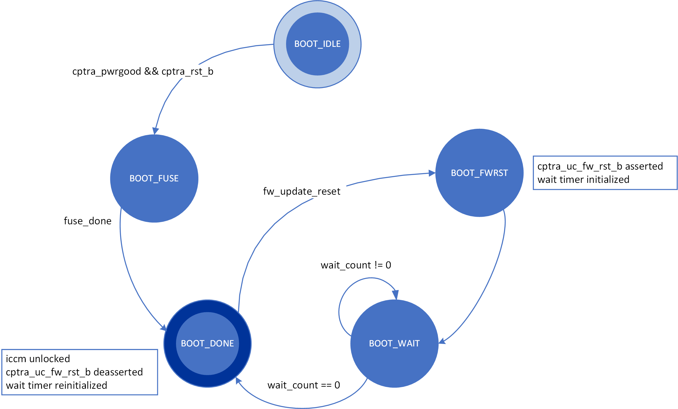 | |
| 289 | 433 | ||
| 290 | -The boot FSM first waits for the SoC to assert cptra\_pwrgood and deassert cptra\_rst\_b. The SoC should wait a minimum of 10 clocks after asserting cptra\_pwrgood before deasserting cptra\_rst\_b. | ||
| 434 | +The boot FSM first waits for the SoC to assert cptra\_pwrgood and deassert cptra\_rst\_b. The SoC first provides a stable clock to Caliptra. After a minimum of 10 clock cycles have elapsed on the stable clock, the SoC asserts cptra\_pwrgood. The SoC waits for a minimum of 10 clocks after asserting cptra\_pwrgood before deasserting cptra\_rst\_b. | ||
| 291 | 435 | In the BOOT\_FUSE state, Caliptra signals to the SoC that it is ready for fuses. After the SoC is done writing fuses, it sets the fuse done register and the FSM advances to BOOT\_DONE. | |
| 292 | 436 | ||
| 293 | 437 | BOOT\_DONE enables Caliptra reset deassertion through a two flip-flop synchronizer. | |
| 294 | 438 | ||
| 295 | 439 | ## SoC access mechanism | |
| 296 | 440 | ||
| 297 | -The SoC communicates with the mailbox through an APB Interface. The SoC acts as the requester with the Caliptra mailbox as the receiver. | ||
| 298 | - | ||
| 299 | -The PAUSER bits are used by the SoC to identify which device is accessing the mailbox. | ||
| 441 | +The SoC communicates with the mailbox through an AXI Interface. The SoC acts as the requester with the Caliptra mailbox as the receiver. | ||
| 442 | + | ||
| 443 | +The AXI_USER bits are used by the SoC to identify which device is accessing the mailbox. | ||
| 300 | 444 | ||
| 301 | 445 | ## Mailbox | |
| 302 | 446 | ||
| 303 | -The Caliptra mailbox is a 128 KiB buffer used for exchanging data between the SoC and the Caliptra microcontroller. | ||
| 447 | +The Caliptra mailbox is a 256 KiB buffer used for exchanging data between the SoC and the Caliptra microcontroller. | ||
| 304 | 448 | ||
| 305 | 449 | When a mailbox is populated by the SoC, initiation of the operation by writing the execute bit triggers an interrupt to the microcontroller. This interrupt indicates that a command is available in the mailbox. The microcontroller is responsible for reading from and responding to the command. | |
| 306 | 450 | ||
| @@ -342,7 +486,8 @@ | |||
| 342 | 486 | Caliptra will not initiate any mailbox commands that require a response from the SoC. Caliptra initiated mailbox commands are “broadcast” and available to any user on the SoC. SoC will not be able to write the DLEN or DATAIN register while processing a Caliptra initiated mailbox command. | |
| 343 | 487 | ||
| 344 | 488 | **Receiving data from the mailbox:** | |
| 345 | -1. On mailbox\_data\_avail assertion, the receiver reads the COMMAND register. | ||
| 489 | + | ||
| 490 | +1. On mailbox\_data\_avail assertion, the receiver reads the COMMAND register. | ||
| 346 | 491 | 2. Receiver reads the DLEN register. | |
| 347 | 492 | 3. Receiver reads the CMD register. | |
| 348 | 493 | 4. Receiver reads the MBOX DATAOUT register. | |
| @@ -358,42 +503,52 @@ | |||
| 358 | 503 | ||
| 359 | 504 | 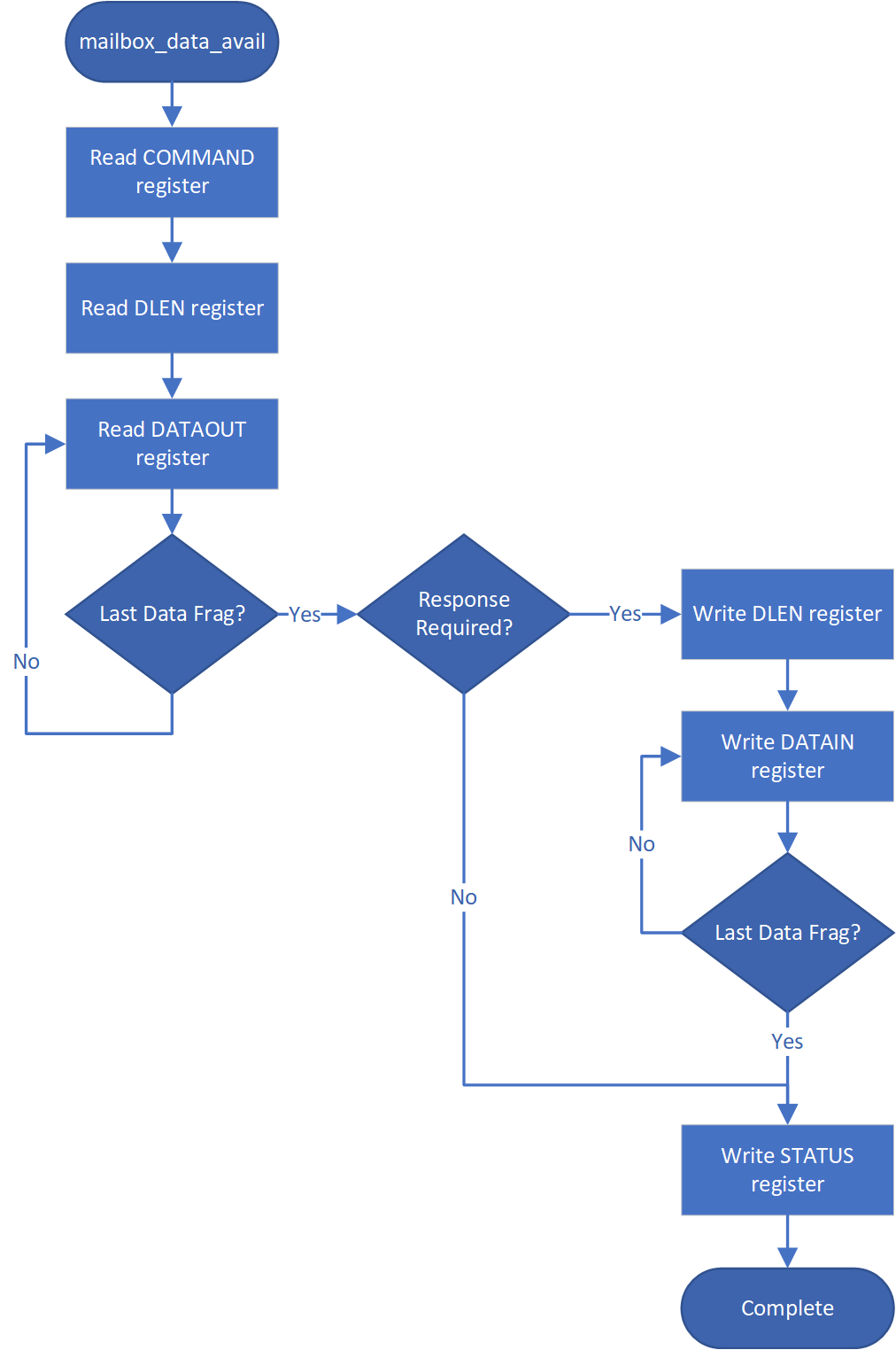 | |
| 360 | 505 | ||
| 506 | +## TAP mailbox mode | ||
| 507 | + | ||
| 508 | +When Caliptra sets the tap_mode register, the mailbox will transition from RDY_FOR_DATA to EXECUTE_TAP instead of EXECUTE_SOC. | ||
| 509 | +This will pass control of the mailbox to the TAP. TAP will follow the **Receiving data from the mailbox** protocol detailed above. | ||
| 510 | + | ||
| 511 | +When TAP acquires the mailbox lock, the mailbox will transition from RDY_FOR_DATA_to EXECUTE_UC. This transition results in the assertion of the internal interrupt signal `uc_mailbox_data_avail` to UC. | ||
| 512 | +This will pass control of the mailbox to the UC. UC will follow the **Receiving data from the mailbox** protocol detailed above. | ||
| 513 | + | ||
| 361 | 514 | ## Mailbox arbitration | |
| 362 | 515 | ||
| 363 | -From a mailbox protocol perspective, as long as CPTRA\_VALID\_PAUSER registers carry valid requestors, mailbox lock can be obtained by any of those valid requestors but only one of them at any given time. While the mailbox flow is happening, all other requestors will not get a grant. | ||
| 516 | +From a mailbox protocol perspective, as long as CPTRA\_VALID\_AXI\_USER registers carry valid requesters, mailbox lock can be obtained by any of those valid requesters but only one of them at any given time. While the mailbox flow is happening, all other requesters will not get a grant. | ||
| 364 | 517 | ||
| 365 | 518 | A request for lock that is denied due to firmware having the lock results in an interrupt to the firmware. Firmware can optionally use this interrupt to release the lock. | |
| 366 | 519 | ||
| 367 | 520 | There is no fair arbitration scheme between SoC and microcontroller. It is first come, first served. When the mailbox is locked for microcontroller use and SoC has unsuccessfully requested the mailbox (due to mailbox actively being used), the mailbox generates an interrupt to the microcontroller as a notification. | |
| 368 | 521 | ||
| 369 | -Further, there is no arbitration between various PAUSER attributes. PAUSER attributes exist for security and filtering reasons only. | ||
| 370 | - | ||
| 371 | -## MAILBOX PAUSER attribute register | ||
| 372 | - | ||
| 373 | -It is strongly recommended that these PAUSER registers are either set at integration time through integration parameters or be programmed by the SoC ROM before any mutable firmware or ROM patches are applied. | ||
| 522 | +Further, there is no arbitration between various AXI_USER attributes. AXI_USER attributes exist for security and filtering reasons only. | ||
| 523 | + | ||
| 524 | +## MAILBOX AXI USER attribute register | ||
| 525 | + | ||
| 526 | +It is strongly recommended that these AXI_USER registers are either set at integration time through integration parameters or be programmed by the SoC ROM before any mutable firmware or ROM patches are applied. | ||
| 527 | + | ||
| 528 | +SoC SHALL not use value 0xFFFFFFFF as a valid AXI user value for any of the below settings. This is reserved for Caliptra-internal usage. | ||
| 374 | 529 | ||
| 375 | 530 | ### Programmable registers | |
| 376 | 531 | ||
| 377 | -Caliptra provides 5 programmable registers that SoC can set at boot time to limit access to the mailbox peripheral. The default PAUSER set by the integration parameter CPTRA\_DEF\_MBOX\_VALID\_PAUSER is valid at all times. CPTRA\_MBOX\_VALID\_PAUSER registers become valid once the corresponding lock bit CPTRA\_MBOX\_PAUSER\_LOCK is set. | ||
| 378 | - | ||
| 379 | -*Table 13: PAUSER register definition* | ||
| 532 | +Caliptra provides 5 programmable registers that SoC can set at boot time to limit access to the mailbox peripheral. The default AXI_USER set by the integration parameter CPTRA\_DEF\_MBOX\_VALID\_AXI\_USER is valid at all times. CPTRA\_MBOX\_VALID\_AXI\_USER registers become valid once the corresponding lock bit CPTRA\_MBOX\_AXI\_USER\_LOCK is set. | ||
| 533 | + | ||
| 534 | +*Table 15: AXI\_USER register definition* | ||
| 380 | 535 | ||
| 381 | 536 | | Register | Description | | |
| 382 | 537 | | :--------- | :--------- | | |
| 383 | -| CPTRA_MBOX_VALID_PAUSER\[4:0\]\[31:0\] | 5 registers for programming PAUSER values that are considered valid for accessing the mailbox protocol. Requests with PAUSER attributes that are not in this list will be ignored. | | ||
| 384 | -| CPTRA_MBOX_PAUSER_LOCK\[4:0\] | 5 registers, bit 0 of each will lock and mark VALID for the corresponding VALID_PAUSER register. | | ||
| 538 | +| CPTRA_MBOX_VALID_AXI_USER\[4:0\]\[31:0\] | 5 registers for programming AXI_USER values that are considered valid for accessing the mailbox protocol. Requests with AXI_USER attributes that are not in this list will be ignored. | | ||
| 539 | +| CPTRA_MBOX_AXI_USER_LOCK\[4:0\] | 5 registers, bit 0 of each will lock and mark VALID for the corresponding VALID_AXI_USER register. | | ||
| 385 | 540 | ||
| 386 | 541 | ||
| 387 | 542 | ### Parameter override | |
| 388 | 543 | ||
| 389 | -Another option for limiting access to the mailbox peripheral are the integration time parameters that override the programmable PAUSER registers. At integration time, the CPTRA\_SET\_MBOX\_PAUSER\_INTEG parameters can be set to 1 which enables the corresponding CPTRA\_MBOX\_VALID\_PAUSER parameters to override the programmable register. | ||
| 390 | - | ||
| 391 | -*Table 14: PAUSER Parameter definition* | ||
| 544 | +Another option for limiting access to the mailbox peripheral are the integration time parameters that override the programmable AXI_USER registers. At integration time, the CPTRA\_SET\_MBOX\_AXI\_USER\_INTEG parameters can be set to 1 which enables the corresponding CPTRA\_MBOX\_VALID\_AXI\_USER parameters to override the programmable register. | ||
| 545 | + | ||
| 546 | +*Table 16: AXI_USER Parameter definition* | ||
| 392 | 547 | ||
| 393 | 548 | | Parameter | Description | | |
| 394 | 549 | | :--------- | :--------- | | |
| 395 | -| CPTRA_SET_MBOX_PAUSER_INTEG\[4:0\] | Setting to 1 enables the corresponding CPTRA_MBOX_VALID_PAUSER parameter. | | ||
| 396 | -| CPTRA_MBOX_VALID_PAUSER\[4:0\] | Value to override programmable PAUSER register at integration time if corresponding CPTRA_SET_MBOX_PAUSER_INTEG parameter is set to 1. | | ||
| 550 | +| CPTRA_SET_MBOX_AXI_USER_INTEG\[4:0\] | Setting to 1 enables the corresponding CPTRA_MBOX_VALID_AXI_USER parameter. | | ||
| 551 | +| CPTRA_MBOX_VALID_AXI_USER\[4:0\] | Value to override programmable AXI_USER register at integration time if corresponding CPTRA_SET_MBOX_AXI_USER_INTEG parameter is set to 1. | | ||
| 397 | 552 | ||
| 398 | 553 | ||
| 399 | 554 | ## Caliptra mailbox protocol | |
| @@ -425,11 +580,11 @@ | |||
| 425 | 580 | * Mailbox protocol violations are reported as fields in the HW ERROR non-fatal register. These events also cause assertion of the cptra\_error\_non\_fatal interrupt signal to SoC. Upon detection, SoC may acknowledge the error by clearing the error field in this register via bus write. | |
| 426 | 581 | * Mailbox protocol violations generate an internal interrupt to the Caliptra microcontroller. Caliptra firmware is aware of the protocol violation. | |
| 427 | 582 | ||
| 428 | -The following table describes APB transactions that cause the Mailbox FSM to enter the ERROR state, given that the register “mbox\_user” contains the value of the APB PAUSER that was used to originally acquire the mailbox lock. | ||
| 429 | - | ||
| 430 | -*Table 15: Mailbox protocol error trigger conditions* | ||
| 431 | - | ||
| 432 | -| FSM state | SoC HAS LOCK | APB PAUSER eq mbox_user | Error state trigger condition | | ||
| 583 | +The following table describes AXI transactions that cause the Mailbox FSM to enter the ERROR state, given that the register “mbox\_user” contains the value of the AXI USER that was used to originally acquire the mailbox lock. | ||
| 584 | + | ||
| 585 | +*Table 17: Mailbox protocol error trigger conditions* | ||
| 586 | + | ||
| 587 | +| FSM state | SoC HAS LOCK | AXI USER eq mbox_user | Error state trigger condition | | ||
| 433 | 588 | | :--------- | :--------- | :--------- | :--------- | | |
| 434 | 589 | | MBOX_RDY_FOR_CMD | 1 | true | Read from mbox_dataout. Write to any register other than mbox_cmd. | | |
| 435 | 590 | | MBOX_RDY_FOR_CMD | 1 | false | \- | | |
| @@ -454,9 +609,9 @@ | |||
| 454 | 609 | ||
| 455 | 610 | ## Overview | |
| 456 | 611 | ||
| 457 | -The SHA acceleration block is in the SoC interface. The SoC can access the accelerator’s hardware API and stream data to be hashed over the APB interface. | ||
| 458 | - | ||
| 459 | -SHA acceleration block uses a similar protocol to the mailbox, but has its own dedicated registers. | ||
| 612 | +The SHA acceleration block is in the SoC interface. The SoC can access the accelerator’s hardware API and stream data to be hashed over the AXI interface. | ||
| 613 | + | ||
| 614 | +SHA acceleration block uses a similar protocol to the mailbox, but has its own dedicated registers. Caliptra is the only permitted user of SHA acceleration, either in streaming mode (via AXI) or in mailbox mode. Use of the SHA acceleration block over AXI is only available in Caliptra Subsystem, and is only available to Caliptra, which will access it via the AXI DMA block. The SHA accelerator checks the AXI AxUSER signal to block any access that originates from an agent other than Caliptra's AXI DMA. | ||
| 460 | 615 | ||
| 461 | 616 | SHA\_LOCK register is set on read. A read of 0 indicates the SHA was unlocked and will now be locked for the requesting user. | |
| 462 | 617 | ||
| @@ -484,7 +639,7 @@ | |||
| 484 | 639 | ||
| 485 | 640 | # TRNG REQ HW API | |
| 486 | 641 | ||
| 487 | -For SoCs that choose to not instantiate Caliptra’s embedded TRNG, we provide a TRNQ REQ HW API. | ||
| 642 | +For SoCs that choose to not instantiate Caliptra’s internal TRNG, we provide a TRNQ REQ HW API. | ||
| 488 | 643 | ||
| 489 | 644 | **While the use of this API is convenient for early enablement, the current | |
| 490 | 645 | Caliptra hardware is unable to provide the same security guarantees with an | |
| @@ -498,12 +653,133 @@ | |||
| 498 | 653 | ||
| 499 | 654 | Having an interface that is separate from the SoC mailbox ensures that this request is not intercepted by any SoC firmware agents (which communicate with SoC mailbox). It is a requirement for FIPS compliance that this TRNG HW API is always handled by SoC hardware gasket logic (and not some SoC ROM or firmware code). | |
| 500 | 655 | ||
| 501 | -TRNG DATA register is tied to TRNG VALID PAUSER. SoC can program the TRNG VALID PAUSER and lock the register using TRNG\_PAUSER\_LOCK[LOCK]. This ensures that TRNG DATA register is read-writeable by only the PAUSER programmed into the TRNG\_VALID\_PAUSER register. If the CPTRA\_TNRG\_PAUSER\_LOCK.LOCK is set to ‘0, then any agent can write to the TRNG DATA register. If the lock is set, only an agent with a specific TRNG\_VALID\_PAUSER can write. | ||
| 656 | +TRNG DATA register is tied to TRNG VALID AXI USER. SoC can program the TRNG VALID AXI USER and lock the register using TRNG\_AXI\_USER\_LOCK[LOCK]. This ensures that TRNG DATA register is read-writeable by only the AXI USER programmed into the TRNG\_VALID\_AXI\_USER register. If the CPTRA\_TNRG\_AXI\_USER\_LOCK.LOCK is set to ‘0, then any agent can write to the TRNG DATA register. If the lock is set, only an agent with a specific TRNG\_VALID\_AXI\_USER can write. | ||
| 502 | 657 | ||
| 503 | 658 | The ROM and firmware currently time out on the TRNG interface after 250,000 | |
| 504 | 659 | attempts to read a DONE bit. This bit is set in the architectural registers, as | |
| 505 | 660 | referenced in 3 in the preceding list. | |
| 506 | 661 | ||
| 662 | +# Internal TRNG | ||
| 663 | + | ||
| 664 | +## TRNG self-test ROM configuration | ||
| 665 | + | ||
| 666 | +The internal TRNG is configured by the ROM to extract entropy used to | ||
| 667 | +initialize Control Flow Integrity (CFI) countermeasures. Since the ROM does not | ||
| 668 | +use entropy for any cryptographic operations, the TRNG self-tests are not | ||
| 669 | +configured for FIPS compliance, but rather to ensure that the quality of the | ||
| 670 | +entropy output is sufficient for ROM operation. | ||
| 671 | + | ||
| 672 | +The default self-test parameters are provided to the ROM via the | ||
| 673 | +`CPTRA_iTRNG_ENTROPY_CONFIG0` and `CPTRA_iTRNG_ENTROPY_CONFIG1` registers. | ||
| 674 | + | ||
| 675 | +The ROM configures self tests with the following parameters. | ||
| 676 | + | ||
| 677 | +### Adaptive test | ||
| 678 | + | ||
| 679 | +The adaptive self-test thresholds are configured as follows if the high and low | ||
| 680 | +thresholds provided in the `CPTRA_iTRNG_ENTROPY_CONFIG0` are non-zero. | ||
| 681 | + | ||
| 682 | +`entropy_src.ADAPTP_HI_THRESHOLDS.FIPS_THRESH` = `CPTRA_iTRNG_ENTROPY_CONFIG0.HIGH_THRESHOLD`\ | ||
| 683 | +`entropy_src.ADAPTP_LO_THRESHOLDS.FIPS_THRESH` = `CPTRA_iTRNG_ENTROPY_CONFIG0.HIGH_THRESHOLD` | ||
| 684 | + | ||
| 685 | +Otherwise, the ROM will use 75% and 25% of the FIPS window size for the default | ||
| 686 | +high and low thresholds. | ||
| 687 | + | ||
| 688 | +`W` = 2048 (bits)\ | ||
| 689 | +`entropy_src.ADAPTP_HI_THRESHOLDS.FIPS_THRESH` = \\(3 * (W / 4)\\) = 1536 \ | ||
| 690 | +`entropy_src.ADAPTP_LO_THRESHOLDS.FIPS_THRESH` = \\(W / 4\\) = 512 | ||
| 691 | + | ||
| 692 | +It is strongly recommended to avoid using the default values. | ||
| 693 | + | ||
| 694 | +### Repetition count test | ||
| 695 | + | ||
| 696 | +Caliptra supports two implementations of the repetition count test, one that | ||
| 697 | +counts repetitions per physical noise source (REPCNT); and, another | ||
| 698 | +that counts repetitions at the symbol level (REPCNTS). The ROM configures | ||
| 699 | +the REPCNT version. | ||
| 700 | + | ||
| 701 | +The self-test is configured as follows if the `CPTRA_iTRNG_ENTROPY_CONFIG1` | ||
| 702 | +register is not zero. | ||
| 703 | + | ||
| 704 | +`entropy_src.REPCNT_THRESHOLDS.FIPS_THRESH` = `CPTRA_iTRNG_ENTROPY_CONFIG1.REPETITION_COUNT` | ||
| 705 | + | ||
| 706 | +Otherwise, the ROM will use a default value configuration: | ||
| 707 | + | ||
| 708 | +`entropy_src.REPCNT_THRESHOLDS.FIPS_THRESH` = 41 | ||
| 709 | + | ||
| 710 | +It is strongly recommended to avoid using the default values. | ||
| 711 | + | ||
| 712 | +### Recommended TRNG self-test thresholds | ||
| 713 | + | ||
| 714 | +The thresholds should be tuned to match the entropy estimate of the | ||
| 715 | +noise source (H), which is calculated by applying a NIST-approved entropy | ||
| 716 | +estimate calculation against raw entropy extracted from the target silicon. | ||
| 717 | + | ||
| 718 | +> Important: It is important to note that the TRNG will discard samples that do | ||
| 719 | +> not pass any of the health tests. Since there is a compression function | ||
| 720 | +> requiring 2048 bits of good entropy to produce a 384 bit seed, the ROM may | ||
| 721 | +> stall if the self-test thresholds are too aggressive or if the values are | ||
| 722 | +> misconfigured. To avoid boot stall issues, it is strongly recommended to | ||
| 723 | +> characterize the noise source on target silicon and select reliable test | ||
| 724 | +> parameters. The ROM only needs to provide sufficient entropy for | ||
| 725 | +> countermeasures, so FIPS-level checks can be performed later, in a less | ||
| 726 | +> boot-timing-sensitive stage. | ||
| 727 | + | ||
| 728 | +The following sections illustrate the self-test parameter configuration. The | ||
| 729 | +`entropy_src` block provides additional tests, but Caliptra's ROM focuses | ||
| 730 | +primarily on the adaptive and repetition count (REPCNT) tests. All other tests | ||
| 731 | +are left with their reset value configuration, which is equivalent to running | ||
| 732 | +the test with the most permissive settings. | ||
| 733 | + | ||
| 734 | +### Test parameters | ||
| 735 | + | ||
| 736 | +The variable names are as defined in NIST SP 800-90B. | ||
| 737 | + | ||
| 738 | +\\(α = 2^{-40}\\) (recommended)\ | ||
| 739 | +\\(H = 0.5\\) (example, implementation specific)\ | ||
| 740 | +\\(W = 2048\\) (constant in ROM/hw) | ||
| 741 | + | ||
| 742 | +### Adaptive proportion test | ||
| 743 | + | ||
| 744 | +The test is configured with to sum all the bits per symbol, due to | ||
| 745 | +`entropy_src.CONF.THRESHOLD_SCOPE` being enabled. The test essentially treats | ||
| 746 | +the combined input as a single binary stream, counting the occurrences of '1's. | ||
| 747 | + | ||
| 748 | +> Note: The `critbinom` function (critical binomial distribution function) is | ||
| 749 | +> implemented by most spreadsheet applications. | ||
| 750 | + | ||
| 751 | +`CPTRA_iTRNG_ENTROPY_CONFIG0.high_threshold` = \\(1 + critbinom(W, 2^{-H}, 1 - α)\\)\ | ||
| 752 | +`CPTRA_iTRNG_ENTROPY_CONFIG0.high_threshold` = \\(1 + critbinom(2048, 2^{-H}, 1 - 2^{-40})\\)\ | ||
| 753 | +`CPTRA_iTRNG_ENTROPY_CONFIG0.high_threshold` = 1591 | ||
| 754 | + | ||
| 755 | +`CPTRA_iTRNG_ENTROPY_CONFIG0.low_threshold` = W - `CPTRA_iTRNG_ENTROPY_CONFIG0.high_threshold`\ | ||
| 756 | +`CPTRA_iTRNG_ENTROPY_CONFIG0.low_threshold` = 2048 - `CPTRA_iTRNG_ENTROPY_CONFIG0.high_threshold`\ | ||
| 757 | +`CPTRA_iTRNG_ENTROPY_CONFIG0.low_threshold` = 457 | ||
| 758 | + | ||
| 759 | +### Repetition count threshold | ||
| 760 | + | ||
| 761 | +The repetition count test as configured in the ROM makes no FIPS compliance | ||
| 762 | +claims due to the fact that counts are aggregated for each individual bit. | ||
| 763 | +This results in a less restrictive threshold as the test will wait for 4x more | ||
| 764 | +repetitions before failing. From an entropy quality perspective, this is | ||
| 765 | +deemed acceptable for the current Caliptra release. | ||
| 766 | + | ||
| 767 | +\\[ | ||
| 768 | +\begin{aligned} | ||
| 769 | +& RcThresh = \frac{-log_2(α)}{H} + 1 \\ | ||
| 770 | +& RcThresh = \frac{40}{H} + 1 \\ | ||
| 771 | +& RcThresh = 81 | ||
| 772 | +\end{aligned} | ||
| 773 | +\\] | ||
| 774 | + | ||
| 775 | +`CPTRA_iTRNG_ENTROPY_CONFIG1.repetition_count` = `RcThresh` = 81 | ||
| 776 | + | ||
| 777 | +### FIPS Compliance | ||
| 778 | + | ||
| 779 | +Caliptra 1.x and 2.0 do not make any FIPS conformance claims on the self-tests | ||
| 780 | +configured by the ROM and executed by the internal TRNG. This is due to the | ||
| 781 | +test configuration. See previous sections for more details. | ||
| 782 | + | ||
| 507 | 783 | # SRAM implementation | |
| 508 | 784 | ||
| 509 | 785 | ## Overview | |
| @@ -524,7 +800,7 @@ | |||
| 524 | 800 | * Instruction Closely-Coupled Memory (ICCM) | |
| 525 | 801 | * Data Closely Coupled Memory (DCCM) | |
| 526 | 802 | ||
| 527 | -Table 4 indicates the signals contained in the memory interface. Direction is relative to the exported memory wrapper that is instantiated outside of the Caliptra subsystem (that is, from the testbench perspective). | ||
| 803 | +Table 7 indicates the signals contained in the memory interface. Direction is relative to the exported memory wrapper that is instantiated outside of the Caliptra subsystem (that is, from the testbench perspective). | ||
| 528 | 804 | ||
| 529 | 805 | ## SRAM timing behavior | |
| 530 | 806 | * [Writes] Input wren signal is asserted simultaneously with input data and address. Input data is stored at the input address 1 clock cycle later. | |
| @@ -539,20 +815,20 @@ | |||
| 539 | 815 | ||
| 540 | 816 | ## SRAM parameterization | |
| 541 | 817 | ||
| 542 | -Parameterization for ICCM/DCCM memories is derived from the configuration of the VeeR RISC-V core that has been selected for Caliptra integration. Parameters defined in the VeeR core determine signal dimensions at the Caliptra top-level interface and drive requirements for SRAM layout. For details about interface parameterization, see the [Interface](#interface) section. The following configuration options from the RISC-V Core dictate this behavior: | ||
| 543 | - | ||
| 544 | -*Table 16: SRAM parameterization* | ||
| 545 | - | ||
| 546 | -| Parameter | Value | Description | | ||
| 547 | -| :--------- | :--------- | :--------- | | ||
| 548 | -| ICCM_ENABLE | 1 | Configures ICCM to be present in VeeR core. | | ||
| 549 | -| ICCM_NUM_BANKS | 4 | Determines the number of physical 39-bit (32-bit data + 7-bit ECC) SRAM blocks that are instantiated in the ICCM. | | ||
| 550 | -| ICCM_INDEX_BITS | 13 | Address bit width for each ICCM Bank that is instantiated. | | ||
| 551 | -| ICCM_SIZE | 128 | Capacity of the ICCM in KiB. Total ICCM capacity in bytes is given by 4 \* ICCM_NUM_BANKS \* 2<sup>ICCM_INDEX_BITS</sup>. | | ||
| 552 | -| DCCM_ENABLE | 1 | Configures DCCM to be present in VeeR core. | | ||
| 553 | -| DCCM_NUM_BANKS | 4 | Determines the number of physical 39-bit (32-bit data + 7-bit ECC) SRAM blocks that are instantiated in the DCCM. | | ||
| 554 | -| DCCM_INDEX_BITS | 13 | Address bit width for each DCCM Bank that is instantiated. | | ||
| 555 | -| DCCM_SIZE | 128 | Capacity of the DCCM in KiB. Total DCCM capacity in bytes is given by 4 \* DCCM_NUM_BANKS \* 2<sup>DCCM_INDEX_BITS</sup>. | | ||
| 818 | +Parameterization for ICCM/DCCM memories is derived from the configuration of the VeeR RISC-V core that has been selected for Caliptra integration. Parameters defined in the VeeR core determine signal dimensions at the Caliptra top-level interface and drive requirements for SRAM layout. For details about interface parameterization, see the [Interface](#interface) section. Complete configuration parameters of the RISC-V Core may be found in [common_defines.sv](../src/riscv_core/veer_el2/rtl/common_defines.sv). The following table explains some parameters that are used to derive interface signal widths for exported RISC-V SRAM signals. | ||
| 819 | + | ||
| 820 | +*Table 18: SRAM parameterization* | ||
| 821 | + | ||
| 822 | +| Parameter | Description | | ||
| 823 | +| :--------- | :--------- | | ||
| 824 | +| ICCM_ENABLE | Configures ICCM to be present in VeeR core. | | ||
| 825 | +| ICCM_NUM_BANKS | Determines the number of physical 39-bit (32-bit data + 7-bit ECC) SRAM blocks that are instantiated in the ICCM. | | ||
| 826 | +| ICCM_INDEX_BITS | Address bit width for each ICCM Bank that is instantiated. | | ||
| 827 | +| ICCM_SIZE | Capacity of the ICCM in KiB. Total ICCM capacity in bytes is given by 4 \* ICCM_NUM_BANKS \* 2<sup>ICCM_INDEX_BITS</sup>. | | ||
| 828 | +| DCCM_ENABLE | Configures DCCM to be present in VeeR core. | | ||
| 829 | +| DCCM_NUM_BANKS | Determines the number of physical 39-bit (32-bit data + 7-bit ECC) SRAM blocks that are instantiated in the DCCM. | | ||
| 830 | +| DCCM_INDEX_BITS | Address bit width for each DCCM Bank that is instantiated. | | ||
| 831 | +| DCCM_SIZE | Capacity of the DCCM in KiB. Total DCCM capacity in bytes is given by 4 \* DCCM_NUM_BANKS \* 2<sup>DCCM_INDEX_BITS</sup>. | | ||
| 556 | 832 | ||
| 557 | 833 | ||
| 558 | 834 | ## Example SRAM machine check reliability integration | |
| @@ -577,11 +853,11 @@ | |||
| 577 | 853 | 6. If no parity error is detected but syndrome == 0 or the syndrome is invalid, the error is deemed uncorrectable. | |
| 578 | 854 | 7. On both single and double errors, the read data is modified before being returned to Caliptra. | |
| 579 | 855 | 8. Since single-bit errors shall be corrected through INTEGRATOR instantiated logic, Caliptra never sees single-bit errors from SRAM. | |
| 580 | -9. Double-bit or uncorrectable errors would cause unpredictable data to be returned to Caliptra. Since this condition shall be detected and reported to MCRIP, there is no concern or expectation that Caliptra will operate correctly after a double error. | ||
| 856 | +9. Double-bit or uncorrectable errors would cause unpredictable data to be returned to Caliptra. Since this condition shall be detected and reported to MCRIP, there is no expectation that Caliptra will operate correctly after a double error. | ||
| 581 | 857 | 10. On detection, single errors are reported as transparent to MCRIP, double errors are reported as fatal. | |
| 582 | 858 | 11. Along with error severity, MCRIP logs physical location of the error. | |
| 583 | 859 | 12. After MCRIP logs an error, it has a choice to send out in-band notification to an external agent. | |
| 584 | -13. MCRIP logs can be queried by SoC software. | ||
| 860 | +13. MCRIP logs can be queried by SoC software. | ||
| 585 | 861 | ||
| 586 | 862 | ### Error injection | |
| 587 | 863 | ||
| @@ -594,26 +870,10 @@ | |||
| 594 | 870 | 2. The non-intrusive error injection does not interfere with the operation of memories. | |
| 595 | 871 | 3. The non-intrusive error injection is functional in Production fused parts. | |
| 596 | 872 | ||
| 597 | -### Caliptra error and recovery flow | ||
| 598 | - | ||
| 599 | -1. Caliptra Stuck: | ||
| 600 | - 1. SoC BC timeout mechanism with 300us timeout. | ||
| 601 | -2. Caliptra reports non-fatal error during boot flow: | ||
| 602 | - 1. cptra\_error\_non\_fatal is an output Caliptra signal, which shall be routed to SoC interrupt controller. | ||
| 603 | - 2. SoC can look at the Caliptra non-fatal error register for error source. | ||
| 604 | - 3. Assume Caliptra can report a non-fatal error at any time. | ||
| 605 | - 4. SoC should monitor the error interrupt or check it before sending any mailbox command. | ||
| 606 | - 5. In the event of a non-fatal error during boot (that is, prior to a ready for RT signal), SoC should enter recovery flow and attempt to boot again using alternate boot part/partition. | ||
| 607 | - 6. If SoC sees that a non-fatal error has occurred AFTER receiving the ready for RT signal, SoC may attempt to recover Caliptra by executing the “Run Self-Test” mailbox command (not yet defined). | ||
| 608 | - 7. If this command completes successfully, SoC may continue using Caliptra as before. | ||
| 609 | - 8. If this command is unsuccessful, Caliptra is in an error state for the remainder of the current boot. | ||
| 610 | - 9. Non-fatal ECC errors are never reported by Caliptra; SoC needs to monitor MCRIP for non-fatal Caliptra ECC errors. | ||
| 611 | -3. Caliptra reports fatal error during boot flow: | ||
| 612 | - 1. cptra\_error\_fatal is an output Caliptra signal, which shall be routed to SoC interrupt controller. | ||
| 613 | - 2. SoC can look at the Caliptra fatal error register for error source. | ||
| 614 | - 3. Assume Caliptra can report a fatal error at any time. | ||
| 615 | - 4. Fatal errors are generally hardware in nature. SoC may attempt to recover by full reset of the entire SoC, or can move on and know that Caliptra will be unavailable for the remainder of the current boot. | ||
| 616 | - 5. We cannot assume that uncorrectable errors will be correctly detected by Caliptra, ECC fatal errors shall be reported by SoC MCRIP. | ||
| 873 | +### Caliptra error handling flow | ||
| 874 | + | ||
| 875 | +1. Any implementation of error and recovery flows must adhere to the error handling requirements specified in [Caliptra.md](https://github.com/chipsalliance/Caliptra/blob/main/doc/Caliptra.md#error-reporting-and-handling) | ||
| 876 | +2. SoC level reporting and handling of fatal & non-fatal errors is product-specific architecture, outside the scope of Caliptra core definition. For example, a CPU and a PCIe device may handle fatal and non-fatal errors differently. | ||
| 617 | 877 | ||
| 618 | 878 | # SoC integration requirements | |
| 619 | 879 | ||
| @@ -621,7 +881,7 @@ | |||
| 621 | 881 | ||
| 622 | 882 | For additional information, see [Caliptra assets and threats](https://github.com/chipsalliance/Caliptra/blob/main/doc/Caliptra.md#caliptra-assets-and-threats). | |
| 623 | 883 | ||
| 624 | -*Table 17: SoC integration requirements* | ||
| 884 | +*Table 19: SoC integration requirements* | ||
| 625 | 885 | ||
| 626 | 886 | | Category | Requirement | Definition of done | Rationale | | |
| 627 | 887 | | :--------- | :--------- | :--------- | :--------- | | |
| @@ -632,7 +892,11 @@ | |||
| 632 | 892 | | Obfuscation Key | For defense in depth, it is strongly recommended that debofuscation key flops are not on the scan chain. <br> Remove the following signals from the scan chain: <br> cptra\_scan\_mode\_Latched\_d <br> cptra\_scan\_mode\_Latched\_f <br> field\_storage.internal\_obf\_key | Statement of conformance | Caliptra HW threat model | | |
| 633 | 893 | | Obfuscation Key | SoC shall ensure that obfuscation key is available (and wires are stable) before Caliptra reset is de-asserted. | Statement of conformance | Functionality and security | | |
| 634 | 894 | | Obfuscation Key | SoC shall implement protections for obfuscation key generation logic and protect against debug/sw/scandump visibility.<br>1. Any flops outside of Caliptra that store obfuscation key or parts of the key should be excluded from scandump.<br>2. SoC shall ensure that the obfuscation key is sent only to Caliptra through HW wires, and it is not visible anywhere outside of Caliptra. | Statement of conformance | Required for Caliptra threat model | | |
| 635 | -| DFT | Before scan is enabled (separate signal that SoC implements on scan insertion), SoC shall set Caliptra's scan\_mode indication to '1 to allow secrets/assets to be flushed. | Statement of conformance | Required by Caliptra threat model | | ||
| 895 | +| CSR HMAC Key | SoC backend flows shall generate CSR signing key with appropriate NIST compliance as dictated in the Caliptra ROT specification. | Statement of conformance | Required by Caliptra threat model | | ||
| 896 | +| CSR HMAC Key | SoC backend flows shall ECO the CSR signing key before tapeout. | Statement of conformance | Required by Caliptra threat model | | ||
| 897 | +| CSR HMAC Key | SoC backend flows should rotate CSR signing key for each project. | Statement of conformance | Required by Caliptra threat model | | ||
| 898 | +| CSR HMAC Key | SoC backend flows should not insert CSR signing key flops into the scan chain. | Statement of conformance | Required by Caliptra threat model | | ||
| 899 | +| DFT | Before scan is enabled (separate signal that SoC implements on scan insertion), SoC shall set Caliptra's scan\_mode indication to '1 for 5,000 clocks to allow secrets/assets to be flushed. | Statement of conformance | Required by Caliptra threat model | | ||
| 636 | 900 | | DFT | Caliptra’s TAP should be a TAP endpoint. | Statement of conformance | Functional requirement | | |
| 637 | 901 | | Mailbox | SoC shall provide an access path between the mailbox and the application CPU complex on SoCs with such complexes (for example, Host CPUs and Smart NICs). See the [Sender Protocol](#sender-protocol) section for details about error conditions. | Statement of conformance | Required for Project Kirkland and TDISP TSM | | |
| 638 | 902 | | Fuses | SoC shall burn non-field fuses during manufacturing. Required vs. optional fuses are listed in the architectural specification. | Test on silicon | Required for UDS threat model | | |
| @@ -646,7 +910,8 @@ | |||
| 646 | 910 | | Fuses | SoCs that intend to undergo FIPS 140-3 zeroization shall expose zeroization API as described in zeroization requirements in architecture specification. SoC shall apply appropriate authentication for this API to protect against denial of service and side channel attacks. | Test on silicon | FIPS 140-3 certification | | |
| 647 | 911 | | Security State | SoC shall drive security state wires in accordance with the SoC's security state. | Statement of conformance | Required for Caliptra threat model | | |
| 648 | 912 | | Security State | If SoC is under debug, then SoC shall drive debug security state to Caliptra. | Statement of conformance | Required for Caliptra threat model | | |
| 649 | -| Resets and Clocks | SoC shall start input clock before caliptra\_pwrgood assertion. | Statement of conformance | Functional | | ||
| 913 | +| Resets and Clocks | SoC shall start input clock before cptra\_pwrgood assertion. The clock must operate for a minimum of 10 clock cycles before SoC asserts cptra\_pwrgood. | Statement of conformance | Functional | | ||
| 914 | +| Resets and Clocks | After asserting cptra\_pwrgood, SoC shall wait for a minimum of 10 clock cycles before deasserting cptra\_rst\_b. | Statement of conformance | Functional | | ||
| 650 | 915 | | Resets and Clocks | SoC reset logic shall assume reset assertions are asynchronous and deassertions are synchronous. | Statement of conformance | Functional | | |
| 651 | 916 | | Resets and Clocks | SoC shall ensure Caliptra's powergood is tied to SoC’s own powergood or any other reset that triggers SoC’s cold boot flow. | Statement of conformance | Required for Caliptra threat model | | |
| 652 | 917 | | Resets and Clocks | SoC shall ensure Caliptra clock is derived from an on-die oscillator circuit. | Statement of conformance | Required for Caliptra threat model | | |
| @@ -658,29 +923,33 @@ | |||
| 658 | 923 | | TRNG | SoC shall provision the Caliptra embedded TRNG with an entropy source if that is used (vs. SoC-shared TRNG API support). | Statement of conformance | Functional | | |
| 659 | 924 | | TRNG | If the TRNG is shared, then upon TRNG\_REQ, SoC shall use immutable logic or code to program Caliptra's TRNG registers. | Statement of conformance | Required for Caliptra threat model and Functional | | |
| 660 | 925 | | SRAMs | SoC shall ensure timing convergence with 1-cycle read path for SRAMs. | Synthesis report | Functional | | |
| 661 | -| SRAMs | SoC shall size SRAMs to account for SECDED. | Statement of conformance | Functional | | ||
| 926 | +| SRAMs | SoC shall size SRAMs to account for SECDED. Exception for Adams-Bridge SRAMs that do not utilize SECDED. | Statement of conformance | Functional | | ||
| 662 | 927 | | SRAMs | SoC shall write-protect fuses that characterize the SRAM. | Statement of conformance | Required for Caliptra threat model | | |
| 663 | 928 | | SRAMs | SoC shall ensure SRAM content is only destroyed on powergood cycling. | Statement of conformance | Functional (Warm Reset, Hitless Update) | | |
| 664 | 929 | | SRAMs | SoC shall only perform SRAM repair on powergood events and prior to caliptra\_rst\_b deassertion. SoC shall also ensure that SRAMs are initialized with all 0 data during powergood events, and prior to caliptra\_rst\_b deassertion. | Statement of conformance | Functional (Warm Reset, Hitless Update) | | |
| 665 | 930 | | Backend convergence | Caliptra supports frequencies up to 400MHz using an industry standard, moderately advanced technology node as of 2023 September. | Statement of conformance | Functional | | |
| 666 | 931 | | Power saving | Caliptra clock gating shall be controlled by Caliptra firmware alone. SoC is provided a global clock gating enable signal (and a register) to control. | Statement of conformance | Required for Caliptra threat model | | |
| 667 | 932 | | Power saving | SoC shall not power-gate Caliptra independently of the entire SoC. | Statement of conformance | Required for Caliptra threat model | | |
| 668 | -| PAUSER | SoC shall drive PAUSER input in accordance with the IP integration spec. | Statement of conformance | Required for Caliptra threat model | | ||
| 933 | +| AXI USER | SoC shall drive AXI USER input for all AXI requests that have a route to Caliptra (e.g. through the AXI interconnect). CANNOT use value 0xFFFFFFFF. This is reserved for Caliptra-internal usage. | Statement of conformance | Required for Caliptra threat model | | ||
| 934 | +| AXI USER | Assigned AXI USER values must be unique for each agent on the interconnect. All SoC AXI agents that have an access path to Caliptra AXI subordinate (or any Caliptra Subsystem components, when using the Subsystem mode) via AXI must either (a) generate AXI transactions using an AXI_USER value that is unique from that used by all other AXI agents on the interconnect or (b) generate AXI transactions using an AXI_USER value that will never overlap with the configured valid AXI users, if the agent is not a valid mailbox user, valid fuse user, or valid trng user. For example, if any AXI agents utilize the AxUSER field for any type of dynamic metadata and are on the same AXI interconnect as Caliptra, all possible AxUSER values from those agents should be avoided for assigning Caliptra VALID AXI USER values. Because AXI AxUSER signals are used to identify accessing agents and enforce access rules, this rule ensures that no single agent may ever generate an AXI transaction that identifies it as originating from a different agent. | Statement of conformance | Required for Caliptra threat model | | ||
| 669 | 935 | | Error reporting | SoC shall report Caliptra error outputs. | Statement of conformance | Telemetry and monitoring | | |
| 670 | 936 | | Error reporting | SoC shall only recover Caliptra fatal errors via SoC power-good reset. | Statement of conformance | Required for Caliptra threat model | | |
| 671 | -| TRNG PAUSER Programming rules | If SoC doesn’t program the CPTRA\_TRNG\_PAUSER\_LOCK\[LOCK\], then Caliptra HW will not accept TRNG data from any SoC entity. | Security | Required for Caliptra threat model | | ||
| 672 | -| TRNG PAUSER Programming rules | If SoC programs CPTRA\_TRNG\_VALID\_PAUSER and sets CPTRA\_TRNG\_PAUSER\_LOCK\[LOCK\], then Caliptra HW will accept TRNG data only from the entity that is programmed into the PAUSER register. | Security | Required for Caliptra threat model | | ||
| 673 | -| TRNG PAUSER Programming rules | It is strongly recommended that these PAUSER registers are either set at integration time through integration parameters or be programmed by the SoC ROM before any mutable FW or ROM patches are absorbed. | Security | Required for Caliptra threat model | | ||
| 674 | -| MAILBOX PAUSER programming rules | 5 PAUSER attribute registers are implemented at SoC interface. | Security | Required for Caliptra threat model | | ||
| 675 | -| MAILBOX PAUSER programming rules | At boot time, a default SoC or PAUSER can access the mailbox. The value of this PAUSER is an integration parameter, CPTRA\_DEF\_MBOX\_VALID\_PAUSER. | Security | Required for Caliptra threat model | | ||
| 676 | -| MAILBOX PAUSER programming rules | The value of CPTRA\_MBOX\_VALID\_PAUSER\[4:0\] register can be programmed by SoC. After it is locked, it becomes a valid PAUSER for accessing the mailbox. | Security | Required for Caliptra threat model | | ||
| 677 | -| MAILBOX PAUSER programming rules | CPTRA\_SET\_MBOX\_PAUSER\_INTEG parameter can be set along with the corresponding CPTRA\_MBOX\_VALID\_PAUSER parameter at integration time. If set, these integration parameters take precedence over the CPTRA\_MBOX\_VALID\_PAUSER\[4:0\] register. | Security | Required for Caliptra threat model | | ||
| 678 | -| MAILBOX PAUSER programming rules | SoC logic (ROM, HW) that is using the Caliptra mailbox right out of cold reset, without first configuring the programmable mailbox PAUSER registers, must send the mailbox accesses with the default PAUSER, CPTRA\_DEF\_MBOX\_VALID\_PAUSER. | Security | Required for Caliptra threat model | | ||
| 679 | -| MAILBOX PAUSER programming rules | For CPTRA\_MBOX\_VALID\_PAUSER\[4:0\], the corresponding lock bits MUST be programmed to ‘1. This enables the mailbox to accept transactions from non-default PAUSERS. | Security | Required for Caliptra threat model | | ||
| 680 | -| MAILBOX PAUSER programming rules | It is strongly recommended that mailbox PAUSER registers are either set at integration time through integration parameters or are programmed by the SoC ROM before any mutable FW or ROM patches are applied. | Security | Required for Caliptra threat model | | ||
| 681 | -| FUSE PAUSER programming rules | 1 PAUSER attribute register is implemented at SoC interface: CPTRA\_FUSE\_VALID\_PAUSER. | Security | Required for Caliptra threat model | | ||
| 682 | -| FUSE PAUSER programming rules | CPTRA\_FUSE\_PAUSER\_LOCK locks the programmable valid pauser register, and marks the programmed value as valid. | Security | Required for Caliptra threat model | | ||
| 683 | -| FUSE PAUSER programming rules | Integrators can choose to harden the valid pauser for fuse access by setting the integration parameter, CPTRA\_FUSE\_VALID\_PAUSER, to the desired value in RTL, and by setting CPTRA\_SET\_FUSE\_PAUSER\_INTEG to 1. If set, these integration parameters take precedence over the CPTRA\_FUSE\_VALID\_PAUSER register. | Security | Required for Caliptra threat model | | ||
| 937 | +| TRNG AXI USER Programming rules | If SoC doesn’t program the CPTRA\_TRNG\_AXI\_USER\_LOCK\[LOCK\] and Caliptra is configured in external TRNG mode, then Caliptra HW will accept TRNG data from any SoC entity. | Security | Required for Caliptra threat model | | ||
| 938 | +| TRNG AXI USER Programming rules | If SoC programs CPTRA\_TRNG\_VALID\_AXI\_USER and sets CPTRA\_TRNG\_AXI\_USER\_LOCK\[LOCK\] and Caliptra is configured in external TRNG mode, then Caliptra HW will accept TRNG data only from the entity that is programmed into the AXI USER register. | Security | Required for Caliptra threat model | | ||
| 939 | +| TRNG AXI USER Programming rules | It is strongly recommended that these AXI USER registers are either set at integration time through integration parameters or be programmed by the SoC ROM before any mutable FW or ROM patches are absorbed. | Security | Required for Caliptra threat model | | ||
| 940 | +| TRNG AXI USER Programming rules | It is strongly recommended that integrators set the TRNG valid AXI_USER to a non-zero value, due to the above uniqueness requirement. | Security | Required for Caliptra threat model | | ||
| 941 | +| MAILBOX AXI USER programming rules | 5 AXI USER attribute registers are implemented at SoC interface. | Security | Required for Caliptra threat model | | ||
| 942 | +| MAILBOX AXI USER programming rules | At boot time, a default SoC or AXI USER can access the mailbox. The value of this AXI USER is an integration parameter, CPTRA\_DEF\_MBOX\_VALID\_AXI\_USER. | Security | Required for Caliptra threat model | | ||
| 943 | +| MAILBOX AXI USER programming rules | The value of CPTRA\_MBOX\_VALID\_AXI\_USER\[4:0\] register can be programmed by SoC. After it is locked, it becomes a valid AXI USER for accessing the mailbox. | Security | Required for Caliptra threat model | | ||
| 944 | +| MAILBOX AXI USER programming rules | CPTRA\_SET\_MBOX\_AXI\_USER\_INTEG parameter can be set along with the corresponding CPTRA\_MBOX\_VALID\_AXI\_USER parameter at integration time. If set, these integration parameters take precedence over the CPTRA\_MBOX\_VALID\_AXI\_USER\[4:0\] register. | Security | Required for Caliptra threat model | | ||
| 945 | +| MAILBOX AXI USER programming rules | SoC logic (ROM, HW) that is using the Caliptra mailbox right out of cold reset, without first configuring the programmable mailbox AXI USER registers, must send the mailbox accesses with the default AXI USER, CPTRA\_DEF\_MBOX\_VALID\_AXI\_USER. | Security | Required for Caliptra threat model | | ||
| 946 | +| MAILBOX AXI USER programming rules | For CPTRA\_MBOX\_VALID\_AXI\_USER\[4:0\], the corresponding lock bits MUST be programmed to ‘1. This enables the mailbox to accept transactions from non-default AXI USERS. | Security | Required for Caliptra threat model | | ||
| 947 | +| MAILBOX AXI USER programming rules | It is strongly recommended that mailbox AXI USER registers are either set at integration time through integration parameters or are programmed by the SoC ROM before any mutable FW or ROM patches are applied. | Security | Required for Caliptra threat model | | ||
| 948 | +| MAILBOX AXI USER Programming rules | It is strongly recommended that integrators set the MAILBOX valid AXI_USER to non-zero values, due to the above uniqueness requirement. | Security | Required for Caliptra threat model | | ||
| 949 | +| FUSE AXI USER programming rules | 1 AXI USER attribute register is implemented at SoC interface: CPTRA\_FUSE\_VALID\_AXI\_USER. | Security | Required for Caliptra threat model | | ||
| 950 | +| FUSE AXI USER programming rules | CPTRA\_FUSE\_AXI\_USER\_LOCK locks the programmable valid axi user register, and marks the programmed value as valid. | Security | Required for Caliptra threat model | | ||
| 951 | +| FUSE AXI USER programming rules | Integrators can choose to harden the valid axi user for fuse access by setting the integration parameter, CPTRA\_FUSE\_VALID\_AXI\_USER, to the desired value in RTL, and by setting CPTRA\_SET\_FUSE\_AXI\_USER\_INTEG to 1. If set, these integration parameters take precedence over the CPTRA\_FUSE\_VALID\_AXI\_USER register. | Security | Required for Caliptra threat model | | ||
| 952 | +| FUSE AXI USER Programming rules | It is strongly recommended that integrators set the FUSE valid AXI_USER to a non-zero value, due to the above uniqueness requirement. | Security | Required for Caliptra threat model | | ||
| 684 | 953 | | Manufacturing | SoC shall provision an IDevID certificate with fields that conform to the requirements described in [Provisioning IDevID during manufacturing](https://github.com/chipsalliance/Caliptra/blob/main/doc/Caliptra.md#provisioning-idevid-during-manufacturing). | Statement of conformance | Functionality | | |
| 685 | 954 | | Manufacturing | Caliptra relies on obfuscation for confidentiality of UDS\_SEED. It is strongly advised to implement manufacturing policies to protect UDS\_SEED as defense in depth measures. <br>1, Prevent leakage of UDS\_SEED on manufacturing floor.<br>2. Implement policies to prevent cloning (programming same UDS\_SEED into multiple devices).<br>3. Implement policies to prevent signing of spurious IDEVID certs. | Statement of conformance | Required for Caliptra threat model | | |
| 686 | 955 | | Chain of trust | SoC shall ensure all mutable code and configuration measurements are stashed into Caliptra. A statement of conformance lists what is considered mutable code and configuration vs. what is not. The statement also describes the start of the boot sequence of the SoC and how Caliptra is incorporated into it. | Statement of conformance | Required for Caliptra threat model | | |
| @@ -689,7 +958,7 @@ | |||
| 689 | 958 | | GLS FEV | GLS FEV must be run to make sure netlist and RTL match and none of the countermeasures are optimized away. See the following table for example warnings from synthesis runs to resolve through FEV | GLS simulations pass | Functional requirement | | |
| 690 | 959 | ||
| 691 | 960 | ||
| 692 | -*Table 18: Caliptra synthesis warnings for FEV evaluation* | ||
| 961 | +*Table 20: Caliptra synthesis warnings for FEV evaluation* | ||
| 693 | 962 | ||
| 694 | 963 | | Module | Warning | Line No. | Description | | |
| 695 | 964 | | :--------- | :--------- | :--------- | :--------- | | |
| @@ -704,12 +973,12 @@ | |||
| 704 | 973 | ||
| 705 | 974 | Several files contain code that may be specific to an integrator's implementation and should be overridden. This overridable code is either configuration parameters with integrator-specific values or modules that implement process-specific functionality. Code in these files should be modified or replaced by integrators using components from the cell library of their fabrication vendor. The following table describes recommended modifications for each file. | |
| 706 | 975 | ||
| 707 | -*Table 19: Caliptra integrator custom RTL file list* | ||
| 976 | +*Table 21: Caliptra integrator custom RTL file list* | ||
| 708 | 977 | ||
| 709 | 978 | | File | Description | | |
| 710 | 979 | | :------------------------------------------------------------------------------------- | :--------------------------------------------------------------------- | | |
| 711 | 980 | | [config_defines.svh](../src/integration/rtl/config_defines.svh) | Enable Caliptra internal TRNG (if applicable).<br>Declare name of custom clock gate module by defining USER_ICG.<br>Enable custom clock gate by defining TECH_SPECIFIC_ICG. | | |
| 712 | -| [soc_ifc_pkg.sv](../src/soc_ifc/rtl/soc_ifc_pkg.sv) | Define PAUSER default behavior and (if applicable) override values. See [Integration Parameters](#integration-parameters). | | ||
| 981 | +| [soc_ifc_pkg.sv](../src/soc_ifc/rtl/soc_ifc_pkg.sv) | Define AXI USER default behavior and (if applicable) override values. See [Integration Parameters](#integration-parameters). | | ||
| 713 | 982 | | [caliptra_icg.sv](../src/libs/rtl/caliptra_icg.sv) | Replace with a technology-specific clock gater.<br>Modifying this file is not necessary if integrators override the clock gate module that is used by setting TECH_SPECIFIC_ICG. | | |
| 714 | 983 | | [beh_lib.sv](../src/riscv_core/veer_el2/rtl/lib/beh_lib.sv) | Replace rvclkhdr/rvoclkhdr with a technology-specific clock gater.<br>Modifying this file may not be necessary if integrators override the clock gate module that is used by setting TECH_SPECIFIC_EC_RV_ICG. | | |
| 715 | 984 | | [beh_lib.sv](../src/riscv_core/veer_el2/rtl/lib/beh_lib.sv) | Replace rvsyncss (and rvsyncss_fpga if the design will be implemented on an FPGA) with a technology-specific sync cell. | | |
| @@ -718,6 +987,58 @@ | |||
| 718 | 987 | | [dmi_jtag_to_core_sync.v](../src/riscv_core/veer_el2/rtl/dmi/dmi_jtag_to_core_sync.v) | Replace with a technology-specific sync cell. This synchronizer implements edge detection logic using a delayed flip flop on the output domain to produce a pulse output. Integrators must take care to ensure logical equivalence when replacing this logic with custom cells. | | |
| 719 | 988 | ||
| 720 | 989 | ||
| 990 | +## Synthesis Constraints | ||
| 991 | + | ||
| 992 | +To ensure the integrity of security countermeasures, silicon integrators **must** apply `size_only` (or an equivalent) constraint to all cells whose instance names contain the `u__size_only__` tag. This prevents synthesis and Place-and-Route (PNR) tools from optimizing away critical redundant logic. | ||
| 993 | + | ||
| 994 | +### Primitive Instantiation | ||
| 995 | + | ||
| 996 | +Caliptra uses redundant logic to counteract Fault Injection (FI) and Side Channel Analysis (SCA). This logic is built using generic primitive modules, which act as placeholders. Integrators must replace these generic primitives with corresponding technology-specific cells from their standard cell library. This abstraction allows for applying the necessary constraints directly to the technology cells. | ||
| 997 | + | ||
| 998 | +The following generic primitives require replacement with technology-specific cells. Ensure the instance names for these replacement cells include the `u__size_only__` tag, as shown in the example below. | ||
| 999 | + | ||
| 1000 | +* `caliptra_prim_generic_and2` | ||
| 1001 | +* `caliptra_prim_generic_buf` | ||
| 1002 | +* `caliptra_prim_generic_clock_mux2` | ||
| 1003 | +* `caliptra_prim_generic_xnor2` | ||
| 1004 | +* `caliptra_prim_generic_xor2` | ||
| 1005 | +* `caliptra_prim_generic_flop` | ||
| 1006 | +* `caliptra_prim_generic_flop_en` | ||
| 1007 | + | ||
| 1008 | +To integrate technology-specific replacements, set the `CALIPTRA_PRIM_MODULE_PREFIX` and `CALIPTRA_PRIM_ROOT` environment variables. For details on how `CALIPTRA_PRIM_MODULE_PREFIX` is used to select between generic and technology-specific modules, see the implementation in [`caliptra_prim_module_name_macros.svh`](../src/caliptra_prim/rtl/caliptra_prim_module_name_macros.svh). | ||
| 1009 | + | ||
| 1010 | +**Example: Technology-Specific Buffer** | ||
| 1011 | + | ||
| 1012 | +The following example shows how to create a technology-specific wrapper for the `caliptra_prim_generic_buf` primitive. | ||
| 1013 | + | ||
| 1014 | +```sv | ||
| 1015 | +// In this example: | ||
| 1016 | +// - `CALIPTRA_PRIM_MODULE_PREFIX` is assumed to be `caliptra_prim_tech_name`. | ||
| 1017 | +// - `TECH_DEPENDENT_BUF` is the name of the technology-specific buffer cell. | ||
| 1018 | +// - `PORT_NAME_IN` and `PORT_NAME_OUT` are its input and output ports. | ||
| 1019 | + | ||
| 1020 | +module caliptra_prim_tech_name_buf #( | ||
| 1021 | + parameter int Width = 1 | ||
| 1022 | +) ( | ||
| 1023 | + input logic [Width-1:0] in_i, | ||
| 1024 | + output logic [Width-1:0] out_o | ||
| 1025 | +); | ||
| 1026 | + | ||
| 1027 | + for (genvar k = 0; k < Width; k++) begin : gen_bufs | ||
| 1028 | + // The instance name "u__size_only__buf" contains the required tag. | ||
| 1029 | + // Synthesis tools must be configured to apply "size_only" | ||
| 1030 | + // constraints to any instance whose name includes "u__size_only__". | ||
| 1031 | + // This naming convention should be used for all replaced primitives. | ||
| 1032 | + | ||
| 1033 | + TECH_DEPENDENT_BUF u__size_only__buf ( | ||
| 1034 | + .<PORT_NAME_IN>(in_i[k]), | ||
| 1035 | + .<PORT_NAME_OUT>(out_o[k]) | ||
| 1036 | + ); | ||
| 1037 | + end | ||
| 1038 | + | ||
| 1039 | +endmodule : caliptra_prim_tech_name_buf | ||
| 1040 | +``` | ||
| 1041 | + | ||
| 721 | 1042 | ||
| 722 | 1043 | # CDC analysis and constraints | |
| 723 | 1044 | ||
| @@ -726,18 +1047,24 @@ | |||
| 726 | 1047 | In an unconstrained environment, several CDC violations are anticipated. CDC analysis requires the addition of constraints to identify valid synchronization mechanisms and/or static/pseudo-static signals. | |
| 727 | 1048 | ||
| 728 | 1049 | ## Analysis of missing synchronizers | |
| 729 | -* All of the signals, whether single-bit or multi-bit, originate from the rvjtag\_tap module internal register on TCK clock, and the Sink/Endpoint is the rvdff register, which is in CalitpraClockDomain clock. | ||
| 730 | -* JTAG does a series of “jtag writes” for each single “register write”. | ||
| 1050 | +* All of the signals, whether single-bit or multi-bit, originate from the CalitpraClockDomain clock and their endpoint is the JTAG clock domain. | ||
| 1051 | +* The violations occur on the read path to the JTAG. | ||
| 731 | 1052 | * We only need to synchronize the controlling signal for this interface. | |
| 732 | -* Inside the dmi\_wrapper, the dmi\_reg\_en and dmi\_reg\_wr\_en comes from dmi\_jtag\_to\_core\_sync, which is a 2FF synchronizer. | ||
| 733 | - | ||
| 734 | -The following code snippet and schematic diagram illustrate JTAG originating CDC violations. | ||
| 1053 | +* Inside the dmi\_wrapper, the dmi\_reg\_en and dmi\_reg\_rd\_en comes from dmi\_jtag\_to\_core\_sync, which is a 2FF synchronizer. | ||
| 1054 | + | ||
| 1055 | +The following code snippets and schematic diagrams illustrate the CDC violations that end at the JTAG interface. | ||
| 735 | 1056 | ||
| 736 | 1057 | *Figure 8: Schematic diagram and code snippet showing JTAG-originating CDC violations* | |
| 737 | 1058 | ||
| 738 | - | ||
| 739 | - | ||
| 740 | - | ||
| 1059 | + | ||
| 1060 | + | ||
| 1061 | + | ||
| 1062 | + | ||
| 1063 | + | ||
| 1064 | + | ||
| 1065 | +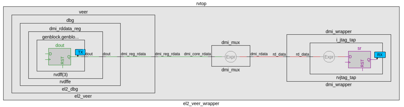 | ||
| 1066 | + | ||
| 1067 | +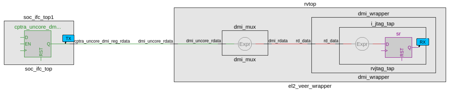 | ||
| 741 | 1068 | ||
| 742 | 1069 | ## CDC analysis conclusions | |
| 743 | 1070 | * Missing synchronizers appear to be the result of “inferred” and/or only 2-FF instantiated synchronizers. | |
| @@ -767,7 +1094,7 @@ | |||
| 767 | 1094 | ### Reset domains | |
| 768 | 1095 | The following table identifies the major reset domains in Caliptra core IP design. | |
| 769 | 1096 | ||
| 770 | -*Table 20: Reset definitions (functional resets are marked in **bold**)* | ||
| 1097 | +*Table 22: Reset definitions (functional resets are marked in **bold**)* | ||
| 771 | 1098 | ||
| 772 | 1099 | | Reset name | Reset type | Reset polarity | Definition point | Reset generated by | | |
| 773 | 1100 | | ---------- | ---------- | -------------- | ---------------- | ------------------ | | |
| @@ -793,7 +1120,7 @@ | |||
| 793 | 1120 | ||
| 794 | 1121 | The following table shows the false paths between various reset groups. | |
| 795 | 1122 | ||
| 796 | -*Table 21: Reset domain crossing false paths* | ||
| 1123 | +*Table 23: Reset domain crossing false paths* | ||
| 797 | 1124 | ||
| 798 | 1125 | | Launch flop reset | Capture flop reset | Comment | | |
| 799 | 1126 | | ------------------ | ------------------ | ------- | | |
| @@ -807,7 +1134,7 @@ | |||
| 807 | 1134 | ||
| 808 | 1135 | ## Reset sequencing scenarios | |
| 809 | 1136 | ||
| 810 | -The resets defined in *Table 20* have the following sequencing phases, which are applicable for different reset scenarios: cold boot, cold reset, warm reset and firmware reset. | ||
| 1137 | +The resets defined in *Table 22* have the following sequencing phases, which are applicable for different reset scenarios: cold boot, cold reset, warm reset and firmware reset. | ||
| 811 | 1138 | ||
| 812 | 1139 | The reset sequencing is illustrated in the following waveform. | |
| 813 | 1140 | ||
| @@ -819,7 +1146,7 @@ | |||
| 819 | 1146 | ||
| 820 | 1147 | The following table defines the order in which resets can get asserted. A ">>" in a cell at row X and column Y indicates that if the reset in row X is asserted, the reset in row Y is also asserted. For rest of the cells (in which symbol ">>" is not present) the preceding assumption is not true and so the paths between those resets are potential RDC violations. The black cells are ignored because they are between the same resets. | |
| 821 | 1148 | ||
| 822 | -*Table 22: Reset sequence ordering constraints* | ||
| 1149 | +*Table 24: Reset sequence ordering constraints* | ||
| 823 | 1150 | ||
| 824 | 1151 | 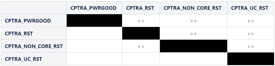 | |
| 825 | 1152 | ||
| @@ -833,7 +1160,7 @@ | |||
| 833 | 1160 | 2. The following debug register, which is driven from JTAG, is not toggled during functional flow. | |
| 834 | 1161 | - u_caliptra.rvtop.veer.dbg.dmcontrol_reg[0] = 0 | |
| 835 | 1162 | 3. Set *scan_mode* to 0 for functional analysis. | |
| 836 | -4. Stamp or create functional resets for *cptra_noncore_rst_b* and *cptra_uc_rst_b* at the definition points, as mentioned in *Table 20*. | ||
| 1163 | +4. Stamp or create functional resets for *cptra_noncore_rst_b* and *cptra_uc_rst_b* at the definition points, as mentioned in *Table 22*. | ||
| 837 | 1164 | 5. Create funtional reset grouping - This step must be customized as per the EDA tool, which is being used for RDC analysis. The goal of this customization is to achieve the following three sequencing requirements/constraints. | |
| 838 | 1165 | - Gate all clocks when *cptra_noncore_rst_b* is asserted. This ensures that the capture flop clock is gated while the source flop's reset is getting asserted, thereby preventing the capture flop from becoming metastable. The result is when *cptra_noncore_rst_b* is going to be asserted, the following signals are constrained to be at 1 at around that time. | |
| 839 | 1166 | - soc_ifc_top1.i_soc_ifc_boot_fsm.rdc_clk_dis | |
| @@ -852,14 +1179,18 @@ | |||
| 852 | 1179 | - sha256.sha256_inst.i_sha256_reg.s_cpuif_req | |
| 853 | 1180 | - csrng.u_reg.u_ahb_slv_sif.dv | |
| 854 | 1181 | - entropy_src.u_reg.u_ahb_slv_sif.dv | |
| 855 | -6. Constrain the RDC false paths as per *Table 21*. | ||
| 1182 | + - aes_inst.ahb_slv_sif_inst.dv | ||
| 1183 | + - aes_inst.aes_clp_reg_inst.s_cpuif_req | ||
| 1184 | + - The AES Core State Machine is assumed to be in the IDLE state | ||
| 1185 | + - aes_inst.aes_inst.u_aes_core.u_aes_control.gen_fsm[0].gen_fsm_p.u_aes_control_fsm_i.u_aes_control_fsm.aes_ctrl_cs[5:0] = 6'b1001 | ||
| 1186 | +6. Constrain the RDC false paths as per *Table 23*. | ||
| 856 | 1187 | ||
| 857 | 1188 | ||
| 858 | 1189 | ## RDC violations and waivers | |
| 859 | 1190 | ||
| 860 | -Considering the given constraints, three sets of crossings were identified as RDC violations. All of them can be waived as explained in *Table 23*. Note that the report may differ across EDA tools due to variations in structural analysis, which can be influenced by a range of settings. | ||
| 861 | - | ||
| 862 | -*Table 23: Reset domain crossing violations* | ||
| 1191 | +Considering the given constraints, three sets of crossings were identified as RDC violations. All of them can be waived as explained in *Table 25*. Note that the report may differ across EDA tools due to variations in structural analysis, which can be influenced by a range of settings. | ||
| 1192 | + | ||
| 1193 | +*Table 25: Reset domain crossing violations* | ||
| 863 | 1194 | ||
| 864 | 1195 | | Sl no | Launch reset | Launch flop | Capture reset | Capture flop | | |
| 865 | 1196 | | ------ | ------------ | ----------- | ------------- | ------------ | | |
| @@ -867,6 +1198,7 @@ | |||
| 867 | 1198 | | 2 | cptra_uc_rst_b | rvtop.veer.dec.tlu.exthaltff.genblock.dff.dout[7] | cptra_noncore_rst_b | cg.user_icg.clk_slcg_0_generated_icg.p_clkgate.vudpi0.q | | |
| 868 | 1199 | | 3 | cptra_uc_rst_b | rvtop.veer.Gen_AXI_To_AHB.lsu_axi4_to_ahb* | cptra_noncore_rst_b | entropy_src.u_entropy_src_core.u_caliptra_prim_packer_fifo_bypass.data_q* | | |
| 869 | 1200 | | 4 | cptra_uc_rst_b | rvtop.veer.Gen_AXI_To_AHB.lsu_axi4_to_ahb* | cptra_noncore_rst_b | entropy_src.u_entropy_src_core.u_caliptra_prim_packer_fifo_precon.data_q* | | |
| 1201 | +| 5 | cptra_rst_b | s_axi_active | cptra_pwrgood | cg.user_soc_ifc_icg.clk_slcg_0_generated_icg.p_clkgate.vudpi0.q | | ||
| 870 | 1202 | ||
| 871 | 1203 | ||
| 872 | 1204 | <br> | |
| @@ -902,7 +1234,7 @@ | |||
| 902 | 1234 | ||
| 903 | 1235 | <br> | |
| 904 | 1236 | ||
| 905 | -*Table 24: Reset domain crossing scenarios for #3 and #4 crossing* | ||
| 1237 | +*Table 26: Reset domain crossing scenarios for #3 and #4 crossing* | ||
| 906 | 1238 | ||
| 907 | 1239 | | #Case | *es_bypass_mode* | *fw_ov_mode_entropy_insert* | *pfifo_bypass_push* | *pfifo_bypass_wdata* | Comment | | |
| 908 | 1240 | | ------ | ---------------- | --------------------------- | ------------------- | -------------------- | ------- | | |
| @@ -913,11 +1245,15 @@ | |||
| 913 | 1245 | ||
| 914 | 1246 | Referring to the preceding table, if it can be ensured that *fw_ov_fifo_wr_pulse* is 0 when *cptra_uc_rst_b* is asserted, RDC crossings (Case #3) can be avoided. This condition is described in the preceding Constraints section. | |
| 915 | 1247 | ||
| 1248 | +For violation in Sl No 5, SOC should ensure that there are no active transactions on the AXI interface while asserting *cptra_rst_b*. | ||
| 1249 | + | ||
| 916 | 1250 | # Synthesis findings | |
| 917 | 1251 | ||
| 918 | -Synthesis experiments have so far found the following: | ||
| 919 | -* Design converges at 400MHz 0.72V using an industry standard, moderately advanced technology node as of 2023 September. | ||
| 920 | -* Design converges at 100MHz using TSMC 40nm process. | ||
| 1252 | +Synthesis has been performed at CALIPTRA_WRAPPER level which encompasses the following :- | ||
| 1253 | +* *caliptra_top* | ||
| 1254 | +* Memories instantiated outside using tech specific macros | ||
| 1255 | + | ||
| 1256 | +Design converges at 400MHz 0.72V using an industry standard, advanced technology node as of 2025 April. | ||
| 921 | 1257 | ||
| 922 | 1258 | Note: Any synthesis warnings of logic optimization must be reviewed and accounted for. | |
| 923 | 1259 | ||
| @@ -929,23 +1265,18 @@ | |||
| 929 | 1265 | ||
| 930 | 1266 | The area is expressed in units of square microns. | |
| 931 | 1267 | ||
| 932 | -The target foundry technology node is an industry standard, moderately advanced technology node as of 2024 June. | ||
| 933 | - | ||
| 934 | -*Table 25: Netlist synthesis data* | ||
| 935 | - | ||
| 936 | -| **IP Name** | **Date** | **Path Group** | **Target Freq** | **QoR WNS** | **QoR Achieveable Freq** | | ||
| 1268 | +The target foundry technology node is an industry standard, advanced technology node as of 2025 April. | ||
| 1269 | + | ||
| 1270 | +*Table 27: Netlist synthesis data* | ||
| 1271 | + | ||
| 1272 | +| **IP Name** | **Combinational Area** | **Sequential Area** | **Memory Area** | **Total Area** | **Instance Count** | | ||
| 937 | 1273 | | :--------- | :--------- | :--------- | :--------- | :--------- | :--------- | | |
| 938 | -| CALIPTRA_WRAPPER | 6/11/2024 | CALIPTRACLK | 500MHz | -0.09 | 500MHz | | ||
| 939 | -| CALIPTRA_WRAPPER | 6/11/2024 | JTAG_TCK | 100MHz | 4606.5 | 100MHz | | ||
| 940 | -| CALIPTRA_WRAPPER | 6/11/2024 | clock_gating_default | 500MHz | 3.36 | 500MHz | | ||
| 941 | -| CALIPTRA_WRAPPER | 6/11/2024 | io_to_flop | 500MHz | 429.8 | 500MHz | | ||
| 942 | -| CALIPTRA_WRAPPER | 6/11/2024 | flop_to_io | 500MHz | 0.10 | 500MHz | | ||
| 943 | - | ||
| 944 | - | ||
| 945 | -| **IP Name** | **Date** | **Stdcell Area** | **Macro Area** | **Memory Area** | **Total Area** | **Flop Count** | **No Clock Regs/Pins Count** | **FM Status** | **FM Eqv Pts** | **FM Non-Eqv Pts** | **FM Abort Pts** | **FM FM**<br> **Non-Comp** **Pts** | | ||
| 946 | -| :--------- | :--------- | :--------- | :--------- | :--------- | :--------- | :--------- | :--------- | :--------- | :--------- | :--------- | :--------- | :--------- | | ||
| 947 | -| CALIPTRA_WRAPPER | 6/11/2024 | 93916 | 0 | 239937 | 341725 | 164505 | 0 | SUCCEEDED | 166241 | 0 | 0 | 0 | | ||
| 948 | - | ||
| 1274 | +| CALIPTRA_WRAPPER | 59934 | 430763 | 319147 | 491159 | 1559238 | | ||
| 1275 | + | ||
| 1276 | + | ||
| 1277 | +*ROM area is not accounted for in the above table.* | ||
| 1278 | + | ||
| 1279 | +NOTE: RTL2Syn formality is not run as of now, we will update the results once we have run the flow. | ||
| 949 | 1280 | ||
| 950 | 1281 | # Recommended LINT rules | |
| 951 | 1282 | ||
| @@ -955,13 +1286,12 @@ | |||
| 955 | 1286 | ||
| 956 | 1287 | The following terminology is used in this document. | |
| 957 | 1288 | ||
| 958 | -*Table 26: Terminology* | ||
| 959 | - | ||
| 1289 | +*Table 28: Terminology* | ||
| 960 | 1290 | ||
| 961 | 1291 | | Abbreviation | Description | | |
| 962 | 1292 | | :--------- | :--------- | | |
| 963 | 1293 | | AHB | AMBA Advanced High-Performance Bus | | |
| 964 | -| APB | AMBA Advanced Peripheral Bus | | ||
| 1294 | +| AXI | AMBA Advanced eXtensible Interface | | ||
| 965 | 1295 | | AES | Advanced Encryption Standard | | |
| 966 | 1296 | | BMD | Boot Media Dependent | | |
| 967 | 1297 | | BMI | Boot Media Integrated | | |
| @@ -972,4 +1302,5 @@ | |||
| 972 | 1302 | | SHA | Secure Hashing Algorithm | | |
| 973 | 1303 | | SPI | Serial Peripheral Interface | | |
| 974 | 1304 | | UART | Universal Asynchronous Receiver Transmitter | | |
| 975 | - | ||
| 1305 | +| UC | Microcontroller, referring to Caliptra's internal RISC-V processor core | | ||
| 1306 | + | ||
Image not present in this version
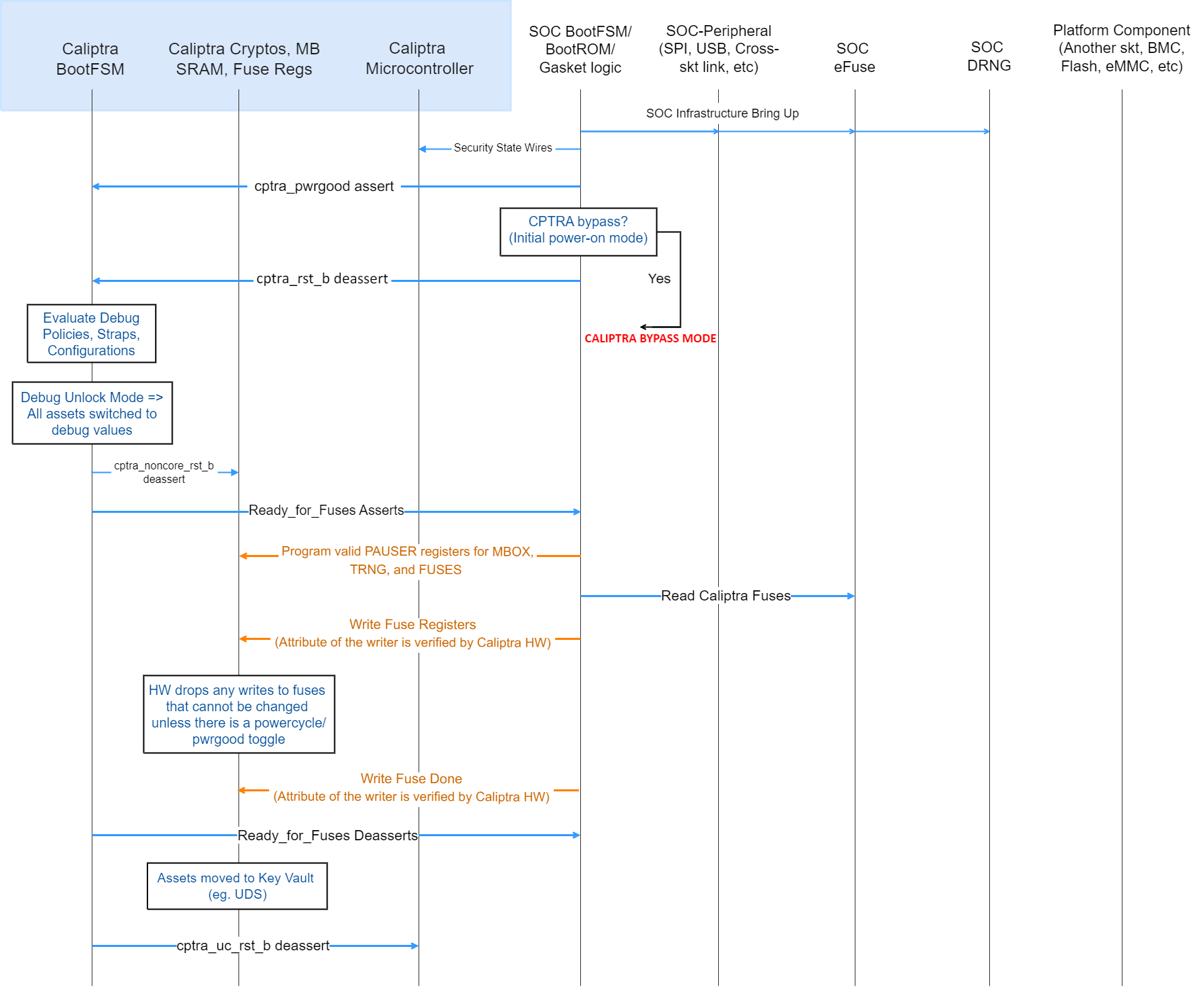

Image not present in this version
Image not present in this version

Image not present in this version

Image not present in this version

Image not present in this version

Image not present in this version
