v1.0: Reset_structure.png
Image not present in this version
v1.1: Reset_structure.png
| @@ -1,12 +1,12 @@ | |||
| 1 | 1 | <div style="font-size: 0.85em; color: #656d76; margin-bottom: 1em; padding: 0.5em; background: #f6f8fa; border-radius: 4px;"> | |
| 2 | -📄 Source: <a href="https://github.com/chipsalliance/caliptra-rtl/blob/e815e542b60d20c1895d7b1bec215ee092f7c3bd/docs/CaliptraIntegrationSpecification.md" target="_blank">chipsalliance/caliptra-rtl/docs/CaliptraIntegrationSpecification.md</a> @ <code>e815e54</code> | ||
| 2 | +📄 Source: <a href="https://github.com/chipsalliance/caliptra-rtl/blob/5f85fb4bc95b753a2f7d042db7dc2644ca1e8c49/docs/CaliptraIntegrationSpecification.md" target="_blank">chipsalliance/caliptra-rtl/docs/CaliptraIntegrationSpecification.md</a> @ <code>5f85fb4</code> | ||
| 3 | 3 | </div> | |
| 4 | 4 | ||
| 5 | 5 |  | |
| 6 | 6 | ||
| 7 | 7 | <p style="text-align: center;">Caliptra Integration Specification</p> | |
| 8 | 8 | ||
| 9 | -<p style="text-align: center;">Version 1.0</p> | ||
| 9 | +<p style="text-align: center;">Version 1.1</p> | ||
| 10 | 10 | ||
| 11 | 11 | <div style="page-break-after: always"></div> | |
| 12 | 12 | ||
| @@ -59,7 +59,7 @@ | |||
| 59 | 59 | | :--------- | :--------- | :--------- | :--------- | | |
| 60 | 60 | | CPTRA_SET_MBOX_PAUSER_INTEG | 5 | soc_ifc_pkg.sv | Each bit hardcodes the valid PAUSER for mailbox at integration time. | | |
| 61 | 61 | | CPTRA_MBOX_VALID_PAUSER | \[4:0\]\[31:0\] | soc_ifc_pkg.sv | Each parameter corresponds to a hardcoded valid PAUSER value for mailbox, set at integration time. Must set corresponding bit in the CPTRA_SET_MBOX_PAUSER_INTEG parameter for this valid pauser override to be used. | | |
| 62 | -| CPTRA_DEF_MBOX_VALID_PAUSER | 32 | soc_ifc_pkg.sv | Sets the default valid PAUSER for mailbox accesses. This PAUSER is valid when any VALID_PAUSER is unlocked or not set by INTEG parameter. | | ||
| 62 | +| CPTRA_DEF_MBOX_VALID_PAUSER | 32 | soc_ifc_pkg.sv | Sets the default valid PAUSER for mailbox accesses. This PAUSER is valid at all times. | | ||
| 63 | 63 | | CPTRA_SET_FUSE_PAUSER_INTEG | 1 | soc_ifc_pkg.sv | Sets the valid PAUSER for fuse accesses at integration time. | | |
| 64 | 64 | | CPTRA_FUSE_VALID_PAUSER | 32 | soc_ifc_pkg.sv | Overrides the programmable valid PAUSER for fuse accesses when CPTRA_SET_FUSE_PAUSER_INTEG is set to 1. | | |
| 65 | 65 | ||
| @@ -157,10 +157,10 @@ | |||
| 157 | 157 | | Signal name | Width | Driver | Synchronous (as viewed from Caliptra’s boundary) | Description | | |
| 158 | 158 | | :--------- | :--------- | :--------- | :--------- | :--------- | | |
| 159 | 159 | | jtag_tck | 1 | input ||| | |
| 160 | -| jtag_tms | 1 | input | Synchronous to tck || | ||
| 161 | -| jtag_tdi | 1 | input | Synchronous to tck || | ||
| 162 | -| jtag_trst_n | 1 | input | Async Deassertion<br> Assertion Synchronous to tck || | ||
| 163 | -| jtag_tdo | 1 | output | Synchronous to tck || | ||
| 160 | +| jtag_tms | 1 | input | Synchronous to jtag_tck || | ||
| 161 | +| jtag_tdi | 1 | input | Synchronous to jtag_tck || | ||
| 162 | +| jtag_trst_n | 1 | input | Asynchronous assertion<br>Synchronous deassertion to jtag_tck || | ||
| 163 | +| jtag_tdo | 1 | output | Synchronous to jtag_tck || | ||
| 164 | 164 | ||
| 165 | 165 | ||
| 166 | 166 | *Table 10: UART interface* | |
| @@ -255,13 +255,13 @@ | |||
| 255 | 255 | ||
| 256 | 256 | The interface signals GENERIC\_INPUT\_WIRES and GENERIC\_OUTPUT\_WIRES are placeholders on the SoC interface reserved for late binding features. This may include any feature that is required for correct operation of the design in the final integrated SoC and that may not be accommodated through existing interface signaling (such as the mailbox). | |
| 257 | 257 | ||
| 258 | -While these late binding interface pins are generic in nature until assigned a function, integrators must not define non-standard use cases for these pins. Defining standard use cases ensures that the security posture of Caliptra in the final implementation is not degraded relative to the consortium design intent. | ||
| 258 | +While these late binding interface pins are generic in nature until assigned a function, integrators must not define non-standard use cases for these pins. Defining standard use cases ensures that the security posture of Caliptra in the final implementation is not degraded relative to the consortium design intent. Bits in GENERIC\_INPUT\_WIRES that don't have a function defined in Caliptra must be tied to a 0-value. These undefined input bits shall not be connected to any flip flops (which would allow run-time transitions on the value). | ||
| 259 | 259 | ||
| 260 | 260 | Each wire connects to a register in the SoC Interface register bank through which communication to the internal microprocessor may be facilitated. Each signal is 64 bits in size. | |
| 261 | 261 | ||
| 262 | 262 | Activity on any bit of the GENERIC\_INPUT\_WIRES triggers a notification interrupt to the microcontroller indicating a bit toggle. | |
| 263 | 263 | ||
| 264 | -The following table describes the allocation of functionality on GENERIC\_INPUT\_WIRES. | ||
| 264 | +The following table describes the allocation of functionality on GENERIC\_INPUT\_WIRES. All bits not listed in this table must be tied to 0. | ||
| 265 | 265 | ||
| 266 | 266 | *Table 12: GENERIC\_INPUT\_WIRES function binding* | |
| 267 | 267 | ||
| @@ -287,7 +287,8 @@ | |||
| 287 | 287 | ||
| 288 | 288 | 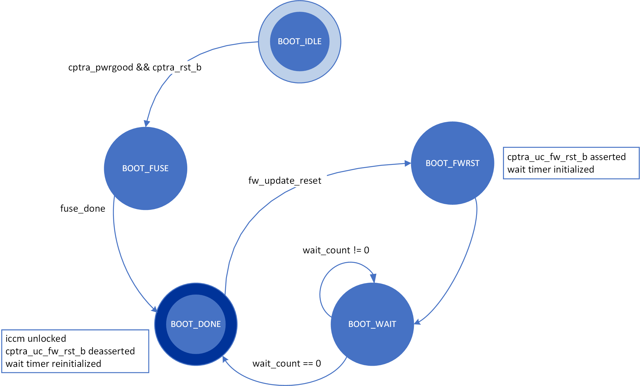 | |
| 289 | 289 | ||
| 290 | -The boot FSM first waits for the SoC to assert cptra\_pwrgood and deassert cptra\_rst\_b. In the BOOT\_FUSE state, Caliptra signals to the SoC that it is ready for fuses. After the SoC is done writing fuses, it sets the fuse done register and the FSM advances to BOOT\_DONE. | ||
| 290 | +The boot FSM first waits for the SoC to assert cptra\_pwrgood and deassert cptra\_rst\_b. The SoC should wait a minimum of 10 clocks after asserting cptra\_pwrgood before deasserting cptra\_rst\_b. | ||
| 291 | +In the BOOT\_FUSE state, Caliptra signals to the SoC that it is ready for fuses. After the SoC is done writing fuses, it sets the fuse done register and the FSM advances to BOOT\_DONE. | ||
| 291 | 292 | ||
| 292 | 293 | BOOT\_DONE enables Caliptra reset deassertion through a two flip-flop synchronizer. | |
| 293 | 294 | ||
| @@ -373,7 +374,7 @@ | |||
| 373 | 374 | ||
| 374 | 375 | ### Programmable registers | |
| 375 | 376 | ||
| 376 | -Caliptra provides 5 programmable registers that SoC can set at boot time to limit access to the mailbox peripheral. The default PAUSER set by the integration parameter CPTRA\_DEF\_MBOX\_VALID\_PAUSER is valid until all programmable registers are consumed. CPTRA\_MBOX\_VALID\_PAUSER registers become valid once the corresponding lock bit CPTRA\_MBOX\_PAUSER\_LOCK is set. | ||
| 377 | +Caliptra provides 5 programmable registers that SoC can set at boot time to limit access to the mailbox peripheral. The default PAUSER set by the integration parameter CPTRA\_DEF\_MBOX\_VALID\_PAUSER is valid at all times. CPTRA\_MBOX\_VALID\_PAUSER registers become valid once the corresponding lock bit CPTRA\_MBOX\_PAUSER\_LOCK is set. | ||
| 377 | 378 | ||
| 378 | 379 | *Table 13: PAUSER register definition* | |
| 379 | 380 | ||
| @@ -428,7 +429,7 @@ | |||
| 428 | 429 | ||
| 429 | 430 | *Table 15: Mailbox protocol error trigger conditions* | |
| 430 | 431 | ||
| 431 | -| FSM state | SOC HAS LOCK | APB PAUSER eq mbox_user | Error state trigger condition | | ||
| 432 | +| FSM state | SoC HAS LOCK | APB PAUSER eq mbox_user | Error state trigger condition | | ||
| 432 | 433 | | :--------- | :--------- | :--------- | :--------- | | |
| 433 | 434 | | MBOX_RDY_FOR_CMD | 1 | true | Read from mbox_dataout. Write to any register other than mbox_cmd. | | |
| 434 | 435 | | MBOX_RDY_FOR_CMD | 1 | false | \- | | |
| @@ -511,7 +512,7 @@ | |||
| 511 | 512 | ||
| 512 | 513 | SRAM repair logic (for example, BIST) and its associated fuses, which are proprietary to companies and their methodologies, is implemented external to the Caliptra boundary. | |
| 513 | 514 | ||
| 514 | -SRAMs must NOT go through BIST or repair flows across a “warm reset”. | ||
| 515 | +SRAMs must NOT go through BIST or repair flows across a “warm reset”. SoC shall perform SRAM repair during a powergood cycling event ("cold reset") and only prior to deasserting cptra\_rst\_b. During powergood cycling events, SoC shall also initialize all entries in the SRAM to a 0 value, prior to deasserting caliptra\_rst\_b. | ||
| 515 | 516 | ||
| 516 | 517 | Mailbox SRAM is implemented with ECC protection. Data width for the mailbox is 32-bits, with 7 parity bits for a Hamming-based SECDED (single-bit error correction and double-bit error detection). | |
| 517 | 518 | ||
| @@ -612,11 +613,13 @@ | |||
| 612 | 613 | 2. SoC can look at the Caliptra fatal error register for error source. | |
| 613 | 614 | 3. Assume Caliptra can report a fatal error at any time. | |
| 614 | 615 | 4. Fatal errors are generally hardware in nature. SoC may attempt to recover by full reset of the entire SoC, or can move on and know that Caliptra will be unavailable for the remainder of the current boot. | |
| 615 | - 5. We cannot assume that uncorrectable errors will be correctly detected by Caliptra, ECC fatal errors shall be reported by SOC MCRIP. | ||
| 616 | + 5. We cannot assume that uncorrectable errors will be correctly detected by Caliptra, ECC fatal errors shall be reported by SoC MCRIP. | ||
| 616 | 617 | ||
| 617 | 618 | # SoC integration requirements | |
| 618 | 619 | ||
| 619 | 620 | The following table describes SoC integration requirements. | |
| 621 | + | ||
| 622 | +For additional information, see [Caliptra assets and threats](https://github.com/chipsalliance/Caliptra/blob/main/doc/Caliptra.md#caliptra-assets-and-threats). | ||
| 620 | 623 | ||
| 621 | 624 | *Table 17: SoC integration requirements* | |
| 622 | 625 | ||
| @@ -626,10 +629,10 @@ | |||
| 626 | 629 | | Obfuscation Key | If not driven through PUF, SoC backend flows shall ECO the obfuscation key before tapeout. | Statement of conformance | Required by UDS and Field Entropy threat model | | |
| 627 | 630 | | Obfuscation Key | Rotation of the obfuscation key (if not driven through PUF) between silicon steppings of a given product (for example, A0 vs. B0 vs. PRQ stepping) is dependent on company-specific policies. | Statement of conformance | Required by UDS and Field Entropy threat model | | |
| 628 | 631 | | Obfuscation Key | SoC backend flows should not insert obfuscation key flops into the scan chain. | Synthesis report | Required by UDS and Field Entropy threat model | | |
| 629 | -| Obfuscation Key | For defense in depth, it is strongly recommended that debofuscation key flops are not on the scan chain. <br> Remove the following signals from the scan chain: <br> cptra_scan_mode_Latched_d <br> cptra_scan_mode_Latched_f <br> field_storage.internal_obf_key | Statement of conformance | Caliptra HW threat model | | ||
| 632 | +| Obfuscation Key | For defense in depth, it is strongly recommended that debofuscation key flops are not on the scan chain. <br> Remove the following signals from the scan chain: <br> cptra\_scan\_mode\_Latched\_d <br> cptra\_scan\_mode\_Latched\_f <br> field\_storage.internal\_obf\_key | Statement of conformance | Caliptra HW threat model | | ||
| 630 | 633 | | Obfuscation Key | SoC shall ensure that obfuscation key is available (and wires are stable) before Caliptra reset is de-asserted. | Statement of conformance | Functionality and security | | |
| 631 | 634 | | Obfuscation Key | SoC shall implement protections for obfuscation key generation logic and protect against debug/sw/scandump visibility.<br>1. Any flops outside of Caliptra that store obfuscation key or parts of the key should be excluded from scandump.<br>2. SoC shall ensure that the obfuscation key is sent only to Caliptra through HW wires, and it is not visible anywhere outside of Caliptra. | Statement of conformance | Required for Caliptra threat model | | |
| 632 | -| DFT | Before scan is enabled (separate signal that SoC implements on scan insertion), SoC shall set Caliptra's scan_mode indication to '1 to allow secrets/assets to be flushed. | Statement of conformance | Required by Caliptra threat model | | ||
| 635 | +| DFT | Before scan is enabled (separate signal that SoC implements on scan insertion), SoC shall set Caliptra's scan\_mode indication to '1 to allow secrets/assets to be flushed. | Statement of conformance | Required by Caliptra threat model | | ||
| 633 | 636 | | DFT | Caliptra’s TAP should be a TAP endpoint. | Statement of conformance | Functional requirement | | |
| 634 | 637 | | Mailbox | SoC shall provide an access path between the mailbox and the application CPU complex on SoCs with such complexes (for example, Host CPUs and Smart NICs). See the [Sender Protocol](#sender-protocol) section for details about error conditions. | Statement of conformance | Required for Project Kirkland and TDISP TSM | | |
| 635 | 638 | | Fuses | SoC shall burn non-field fuses during manufacturing. Required vs. optional fuses are listed in the architectural specification. | Test on silicon | Required for UDS threat model | | |
| @@ -637,47 +640,52 @@ | |||
| 637 | 640 | | Fuses | SoC shall write fuse registers and fuse done via immutable logic or ROM code. | Statement of conformance | Required for Caliptra threat model | | |
| 638 | 641 | | Fuses | SoC shall expose an API for programming Field Entropy as described in the architecture documentation. SoC shall ensure that Field Entropy can only be programmed via this API and shall explicitly prohibit burning of discrete Field Entropy bits and re-burning of already burned Field Entropy entries. | Test on silicon | Required for Field Entropy | | |
| 639 | 642 | | Fuses | SoC shall ensure that any debug read paths for fuses are disabled in PRODUCTION lifecycle state. | Test on silicon | Required for Field Entropy | | |
| 640 | -| Fuses | SoC shall ensure that UDS_SEED and Field Entropy supplied to Caliptra come directly from OTP fuses and there are no debug paths to inject new values. | Statement of conformance | Required for Caliptra Threat model | | ||
| 643 | +| Fuses | SoC shall ensure that UDS\_SEED and Field Entropy supplied to Caliptra come directly from OTP fuses and there are no debug paths to inject new values. | Statement of conformance | Required for Caliptra threat model | | ||
| 641 | 644 | | Fuses | SoC shall add integrity checks for Caliptra fuses as per SoC policy. | Statement of conformance | Reliability | | |
| 642 | -| Fuses | SoC should apply shielding/obfuscation measures to protect fuse macro. | Statement of conformance | Required for Caliptra Threat model | | ||
| 645 | +| Fuses | SoC should apply shielding/obfuscation measures to protect fuse macro. | Statement of conformance | Required for Caliptra threat model | | ||
| 643 | 646 | | Fuses | SoCs that intend to undergo FIPS 140-3 zeroization shall expose zeroization API as described in zeroization requirements in architecture specification. SoC shall apply appropriate authentication for this API to protect against denial of service and side channel attacks. | Test on silicon | FIPS 140-3 certification | | |
| 644 | 647 | | Security State | SoC shall drive security state wires in accordance with the SoC's security state. | Statement of conformance | Required for Caliptra threat model | | |
| 645 | 648 | | Security State | If SoC is under debug, then SoC shall drive debug security state to Caliptra. | Statement of conformance | Required for Caliptra threat model | | |
| 646 | -| Resets and Clocks | SoC shall start input clock before caliptra_pwrgood assertion. | Statement of conformance | Functional | | ||
| 649 | +| Resets and Clocks | SoC shall start input clock before caliptra\_pwrgood assertion. | Statement of conformance | Functional | | ||
| 647 | 650 | | Resets and Clocks | SoC reset logic shall assume reset assertions are asynchronous and deassertions are synchronous. | Statement of conformance | Functional | | |
| 648 | 651 | | Resets and Clocks | SoC shall ensure Caliptra's powergood is tied to SoC’s own powergood or any other reset that triggers SoC’s cold boot flow. | Statement of conformance | Required for Caliptra threat model | | |
| 652 | +| Resets and Clocks | SoC shall ensure Caliptra clock is derived from an on-die oscillator circuit. | Statement of conformance | Required for Caliptra threat model | | ||
| 653 | +| Resets and Clocks | SoC shall ensure that any programmable Caliptra clock controls are restricted to the SoC Manager. | Statement of conformance | Required for Caliptra threat model | | ||
| 654 | +| Resets and Clocks | SoC should defend against external clock stop attacks. | Statement of conformance | Required for Caliptra threat model | | ||
| 655 | +| Resets and Clocks | SoC should defend against external clock glitching attacks. | Statement of conformance | Required for Caliptra threat model | | ||
| 656 | +| Resets and Clocks | SoC should defend against external clock overclocking attacks. | Statement of conformance | Required for Caliptra threat model | | ||
| 649 | 657 | | TRNG | SoC shall either provision Caliptra with a dedicated TRNG or shared TRNG. It is highly recommended to use dedicated ITRNG | Statement of conformance | Required for Caliptra threat model and Functional | | |
| 650 | 658 | | TRNG | SoC shall provision the Caliptra embedded TRNG with an entropy source if that is used (vs. SoC-shared TRNG API support). | Statement of conformance | Functional | | |
| 651 | -| TRNG | If the TRNG is shared, then upon TRNG_REQ, SoC shall use immutable logic or code to program Caliptra's TRNG registers. | Statement of conformance | Required for Caliptra threat model and Functional | | ||
| 659 | +| TRNG | If the TRNG is shared, then upon TRNG\_REQ, SoC shall use immutable logic or code to program Caliptra's TRNG registers. | Statement of conformance | Required for Caliptra threat model and Functional | | ||
| 652 | 660 | | SRAMs | SoC shall ensure timing convergence with 1-cycle read path for SRAMs. | Synthesis report | Functional | | |
| 653 | 661 | | SRAMs | SoC shall size SRAMs to account for SECDED. | Statement of conformance | Functional | | |
| 654 | 662 | | SRAMs | SoC shall write-protect fuses that characterize the SRAM. | Statement of conformance | Required for Caliptra threat model | | |
| 655 | 663 | | SRAMs | SoC shall ensure SRAM content is only destroyed on powergood cycling. | Statement of conformance | Functional (Warm Reset, Hitless Update) | | |
| 656 | -| SRAMs | SoC shall only perform SRAM repair on powergood events and prior to caliptra_rst_b deassertion. | Statement of conformance | Functional (Warm Reset, Hitless Update) | | ||
| 657 | -| Backend convergence | Caliptra supports frequencies up to 400MHz using an industry standard, moderately advanced technology node as of 2023 September. || Functional | | ||
| 658 | -| Power saving | Caliptra clock gating shall be controlled by Caliptra firmware alone. SoC is provided a global clock gating enable signal (and a register) to control. || Required for Caliptra threat model | | ||
| 664 | +| SRAMs | SoC shall only perform SRAM repair on powergood events and prior to caliptra\_rst\_b deassertion. SoC shall also ensure that SRAMs are initialized with all 0 data during powergood events, and prior to caliptra\_rst\_b deassertion. | Statement of conformance | Functional (Warm Reset, Hitless Update) | | ||
| 665 | +| Backend convergence | Caliptra supports frequencies up to 400MHz using an industry standard, moderately advanced technology node as of 2023 September. | Statement of conformance | Functional | | ||
| 666 | +| Power saving | Caliptra clock gating shall be controlled by Caliptra firmware alone. SoC is provided a global clock gating enable signal (and a register) to control. | Statement of conformance | Required for Caliptra threat model | | ||
| 659 | 667 | | Power saving | SoC shall not power-gate Caliptra independently of the entire SoC. | Statement of conformance | Required for Caliptra threat model | | |
| 660 | -| PAUSER | SoC shall drive PAUSER input in accordance with the IP integration spec. | Statement of conformance | ? | | ||
| 668 | +| PAUSER | SoC shall drive PAUSER input in accordance with the IP integration spec. | Statement of conformance | Required for Caliptra threat model | | ||
| 661 | 669 | | Error reporting | SoC shall report Caliptra error outputs. | Statement of conformance | Telemetry and monitoring | | |
| 662 | 670 | | Error reporting | SoC shall only recover Caliptra fatal errors via SoC power-good reset. | Statement of conformance | Required for Caliptra threat model | | |
| 663 | -| TRNG PAUSER Programming rules | If SoC doesn’t program the CPTRA_TRNG_PAUSER_LOCK\[LOCK\], then Caliptra HW will not accept TRNG data from any SoC entity. | Security | Required for Caliptra threat model | | ||
| 664 | -| TRNG PAUSER Programming rules | If SoC programs CPTRA_TRNG_VALID_PAUSER and sets CPTRA_TRNG_PAUSER_LOCK\[LOCK\], then Caliptra HW will accept TRNG data only from the entity that is programmed into the PAUSER register. | Security | Required for Caliptra threat model | | ||
| 671 | +| TRNG PAUSER Programming rules | If SoC doesn’t program the CPTRA\_TRNG\_PAUSER\_LOCK\[LOCK\], then Caliptra HW will not accept TRNG data from any SoC entity. | Security | Required for Caliptra threat model | | ||
| 672 | +| TRNG PAUSER Programming rules | If SoC programs CPTRA\_TRNG\_VALID\_PAUSER and sets CPTRA\_TRNG\_PAUSER\_LOCK\[LOCK\], then Caliptra HW will accept TRNG data only from the entity that is programmed into the PAUSER register. | Security | Required for Caliptra threat model | | ||
| 665 | 673 | | TRNG PAUSER Programming rules | It is strongly recommended that these PAUSER registers are either set at integration time through integration parameters or be programmed by the SoC ROM before any mutable FW or ROM patches are absorbed. | Security | Required for Caliptra threat model | | |
| 666 | 674 | | MAILBOX PAUSER programming rules | 5 PAUSER attribute registers are implemented at SoC interface. | Security | Required for Caliptra threat model | | |
| 667 | -| MAILBOX PAUSER programming rules | At boot time, a default SoC or PAUSER can access the mailbox. The value of this PAUSER is an integration parameter, CPTRA_DEF_MBOX_VALID_PAUSER. | Security | Required for Caliptra threat model | | ||
| 668 | -| MAILBOX PAUSER programming rules | The value of CPTRA_MBOX_VALID_PAUSER\[4:0\] register can be programmed by SoC. After it is locked, it becomes a valid PAUSER for accessing the mailbox. | Security | Required for Caliptra threat model | | ||
| 669 | -| MAILBOX PAUSER programming rules | Alternatively, CPTRA_SET_MBOX_PAUSER_INTEG parameter can be set along with the corresponding CPTRA_MBOX_VALID_PAUSER parameter at integration time. | Security | Required for Caliptra threat model | | ||
| 670 | -| MAILBOX PAUSER programming rules | SoC logic (ROM, HW) that is using the Caliptra mailbox right out of cold reset, without first configuring the programmable mailbox PAUSER registers, must send the mailbox accesses with the default PAUSER, CPTRA_DEF_MBOX_VALID_PAUSER. | Security | Required for Caliptra threat model | | ||
| 671 | -| MAILBOX PAUSER programming rules | For CPTRA_MBOX_VALID_PAUSER\[4:0\], the corresponding lock bits MUST be programmed to ‘1. This enables the mailbox to accept transactions from non-default PAUSERS. | Security | Required for Caliptra threat model | | ||
| 672 | -| MAILBOX PAUSER programming rules | It is strongly recommended that these PAUSER registers are either set at integration time through integration parameters or be programmed by the SoC ROM before any mutable FW or ROM patches are applied. | Security | Required for Caliptra threat model | | ||
| 673 | -| FUSE PAUSER programming rules | 1 PAUSER attribute register is implemented at SoC interface: CPTRA_FUSE_VALID_PAUSER. ||| | ||
| 674 | -| FUSE PAUSER programming rules | CPTRA_FUSE_PAUSER_LOCK locks the programmable valid pauser register, and marks the programmed value as valid. ||| | ||
| 675 | -| FUSE PAUSER programming rules | Integrators can choose to harden the valid pauser for fuse access by setting the integration parameter, CPTRA_FUSE_VALID_PAUSER, to the desired value in RTL, and by setting CPTRA_SET_FUSE_PAUSER_INTEG to 1. ||| | ||
| 675 | +| MAILBOX PAUSER programming rules | At boot time, a default SoC or PAUSER can access the mailbox. The value of this PAUSER is an integration parameter, CPTRA\_DEF\_MBOX\_VALID\_PAUSER. | Security | Required for Caliptra threat model | | ||
| 676 | +| MAILBOX PAUSER programming rules | The value of CPTRA\_MBOX\_VALID\_PAUSER\[4:0\] register can be programmed by SoC. After it is locked, it becomes a valid PAUSER for accessing the mailbox. | Security | Required for Caliptra threat model | | ||
| 677 | +| MAILBOX PAUSER programming rules | CPTRA\_SET\_MBOX\_PAUSER\_INTEG parameter can be set along with the corresponding CPTRA\_MBOX\_VALID\_PAUSER parameter at integration time. If set, these integration parameters take precedence over the CPTRA\_MBOX\_VALID\_PAUSER\[4:0\] register. | Security | Required for Caliptra threat model | | ||
| 678 | +| MAILBOX PAUSER programming rules | SoC logic (ROM, HW) that is using the Caliptra mailbox right out of cold reset, without first configuring the programmable mailbox PAUSER registers, must send the mailbox accesses with the default PAUSER, CPTRA\_DEF\_MBOX\_VALID\_PAUSER. | Security | Required for Caliptra threat model | | ||
| 679 | +| MAILBOX PAUSER programming rules | For CPTRA\_MBOX\_VALID\_PAUSER\[4:0\], the corresponding lock bits MUST be programmed to ‘1. This enables the mailbox to accept transactions from non-default PAUSERS. | Security | Required for Caliptra threat model | | ||
| 680 | +| MAILBOX PAUSER programming rules | It is strongly recommended that mailbox PAUSER registers are either set at integration time through integration parameters or are programmed by the SoC ROM before any mutable FW or ROM patches are applied. | Security | Required for Caliptra threat model | | ||
| 681 | +| FUSE PAUSER programming rules | 1 PAUSER attribute register is implemented at SoC interface: CPTRA\_FUSE\_VALID\_PAUSER. | Security | Required for Caliptra threat model | | ||
| 682 | +| FUSE PAUSER programming rules | CPTRA\_FUSE\_PAUSER\_LOCK locks the programmable valid pauser register, and marks the programmed value as valid. | Security | Required for Caliptra threat model | | ||
| 683 | +| FUSE PAUSER programming rules | Integrators can choose to harden the valid pauser for fuse access by setting the integration parameter, CPTRA\_FUSE\_VALID\_PAUSER, to the desired value in RTL, and by setting CPTRA\_SET\_FUSE\_PAUSER\_INTEG to 1. If set, these integration parameters take precedence over the CPTRA\_FUSE\_VALID\_PAUSER register. | Security | Required for Caliptra threat model | | ||
| 676 | 684 | | Manufacturing | SoC shall provision an IDevID certificate with fields that conform to the requirements described in [Provisioning IDevID during manufacturing](https://github.com/chipsalliance/Caliptra/blob/main/doc/Caliptra.md#provisioning-idevid-during-manufacturing). | Statement of conformance | Functionality | | |
| 677 | -| Manufacturing | Caliptra relies on obfuscation for confidentiality of UDS_SEED. It is strongly advised to implement manufacturing policies to protect UDS_SEED as defense in depth measures. <br>1, Prevent leakage of UDS_SEED on manufacturing floor.<br>2. Implement policies to prevent cloning (programming same UDS_SEED into multiple devices).<br>3. Implement policies to prevent signing of spurious IDEVID certs. | Statement of conformance | Required for Caliptra Threat model | | ||
| 678 | -| Chain of trust | SoC shall ensure all mutable code and configuration measurements are stashed into Caliptra. A statement of conformance lists what is considered mutable code and configuration vs. what is not. The statement also describes the start of the boot sequence of the SoC and how Caliptra is incorporated into it. | Statement of conformance | Required for Caliptra Threat model | | ||
| 679 | -| Chain of trust | SoC shall limit the mutable code and configuration that persists across the Caliptra powergood reset. A statement of conformance lists what persists and why this persistence is necessary. | Statement of conformance | Required for Caliptra Threat model | | ||
| 680 | -| Implementation | SoC shall apply size-only constraints on cells tagged with the "u__size_only__" string and shall ensure that these are not optimized in synthesis and PNR | Statement of conformance | Required for Caliptra Threat model | | ||
| 685 | +| Manufacturing | Caliptra relies on obfuscation for confidentiality of UDS\_SEED. It is strongly advised to implement manufacturing policies to protect UDS\_SEED as defense in depth measures. <br>1, Prevent leakage of UDS\_SEED on manufacturing floor.<br>2. Implement policies to prevent cloning (programming same UDS\_SEED into multiple devices).<br>3. Implement policies to prevent signing of spurious IDEVID certs. | Statement of conformance | Required for Caliptra threat model | | ||
| 686 | +| Chain of trust | SoC shall ensure all mutable code and configuration measurements are stashed into Caliptra. A statement of conformance lists what is considered mutable code and configuration vs. what is not. The statement also describes the start of the boot sequence of the SoC and how Caliptra is incorporated into it. | Statement of conformance | Required for Caliptra threat model | | ||
| 687 | +| Chain of trust | SoC shall limit the mutable code and configuration that persists across the Caliptra powergood reset. A statement of conformance lists what persists and why this persistence is necessary. | Statement of conformance | Required for Caliptra threat model | | ||
| 688 | +| Implementation | SoC shall apply size-only constraints on cells tagged with the "u\_\_size\_only\_\_" string and shall ensure that these are not optimized in synthesis and PNR | Statement of conformance | Required for Caliptra threat model | | ||
| 681 | 689 | | GLS FEV | GLS FEV must be run to make sure netlist and RTL match and none of the countermeasures are optimized away. See the following table for example warnings from synthesis runs to resolve through FEV | GLS simulations pass | Functional requirement | | |
| 682 | 690 | ||
| 683 | 691 | ||
| @@ -702,11 +710,12 @@ | |||
| 702 | 710 | | :------------------------------------------------------------------------------------- | :--------------------------------------------------------------------- | | |
| 703 | 711 | | [config_defines.svh](../src/integration/rtl/config_defines.svh) | Enable Caliptra internal TRNG (if applicable).<br>Declare name of custom clock gate module by defining USER_ICG.<br>Enable custom clock gate by defining TECH_SPECIFIC_ICG. | | |
| 704 | 712 | | [soc_ifc_pkg.sv](../src/soc_ifc/rtl/soc_ifc_pkg.sv) | Define PAUSER default behavior and (if applicable) override values. See [Integration Parameters](#integration-parameters). | | |
| 705 | -| [caliptra_icg.sv](../src/libs/rtl/caliptra_icg.sv) | Replace with technology-specific clock gater.<br>Modifying this file is not necessary if integrators override the clock gate module that is used by setting TECH_SPECIFIC_ICG. | | ||
| 706 | -| [beh_lib.sv](../src/riscv_core/veer_el2/rtl/lib/beh_lib.sv) | Replace rvclkhdr/rvoclkhdr with technology-specific clock gater.<br>Modifying this file may not be necessary if integrators override the clock gate module that is used by setting TECH_SPECIFIC_EC_RV_ICG. | | ||
| 707 | -| [caliptra_prim_flop_2sync.sv](../src/caliptra_prim/rtl/caliptra_prim_flop_2sync.sv) | Replace with technology-specific sync cell. | | ||
| 708 | -| [caliptra_2ff_sync.sv](../src/libs/rtl/caliptra_2ff_sync.sv) | Replace with technology-specific sync cell. | | ||
| 709 | -| [dmi_jtag_to_core_sync.v](../src/riscv_core/veer_el2/rtl/dmi/dmi_jtag_to_core_sync.v) | Replace with technology-specific sync cell. | | ||
| 713 | +| [caliptra_icg.sv](../src/libs/rtl/caliptra_icg.sv) | Replace with a technology-specific clock gater.<br>Modifying this file is not necessary if integrators override the clock gate module that is used by setting TECH_SPECIFIC_ICG. | | ||
| 714 | +| [beh_lib.sv](../src/riscv_core/veer_el2/rtl/lib/beh_lib.sv) | Replace rvclkhdr/rvoclkhdr with a technology-specific clock gater.<br>Modifying this file may not be necessary if integrators override the clock gate module that is used by setting TECH_SPECIFIC_EC_RV_ICG. | | ||
| 715 | +| [beh_lib.sv](../src/riscv_core/veer_el2/rtl/lib/beh_lib.sv) | Replace rvsyncss (and rvsyncss_fpga if the design will be implemented on an FPGA) with a technology-specific sync cell. | | ||
| 716 | +| [caliptra_prim_flop_2sync.sv](../src/caliptra_prim/rtl/caliptra_prim_flop_2sync.sv) | Replace with a technology-specific sync cell. | | ||
| 717 | +| [caliptra_2ff_sync.sv](../src/libs/rtl/caliptra_2ff_sync.sv) | Replace with a technology-specific sync cell. | | ||
| 718 | +| [dmi_jtag_to_core_sync.v](../src/riscv_core/veer_el2/rtl/dmi/dmi_jtag_to_core_sync.v) | Replace with a technology-specific sync cell. This synchronizer implements edge detection logic using a delayed flip flop on the output domain to produce a pulse output. Integrators must take care to ensure logical equivalence when replacing this logic with custom cells. | | ||
| 710 | 719 | ||
| 711 | 720 | ||
| 712 | 721 | ||
| @@ -739,12 +748,170 @@ | |||
| 739 | 748 | * Pseudo-static: wr\_data, wr\_addr | |
| 740 | 749 | * cdc signal reg\_wr\_data -module dmi\_wrapper -stable | |
| 741 | 750 | * cdc signal reg\_wr\_addr -module dmi\_wrapper -stable | |
| 742 | -* The core clock frequency must be at least twice the TCK clock frequency for the JTAG data to pass correctly through the synchronizers. | ||
| 751 | +* The core clock frequency must be at least twice the TCK clock frequency for the JTAG data to pass correctly through the synchronizers. | ||
| 743 | 752 | ||
| 744 | 753 | ## CDC constraints | |
| 745 | 754 | * cdc report scheme two\_dff -severity violation | |
| 746 | 755 | * cdc signal reg\_wr\_data -module dmi\_wrapper -stable | |
| 747 | 756 | * cdc signal reg\_wr\_addr -module dmi\_wrapper -stable | |
| 757 | +* cdc signal rd\_data -module dmi\_wrapper -stable | ||
| 758 | + | ||
| 759 | +# RDC analysis and constraints | ||
| 760 | + | ||
| 761 | +Reset Domain Crossing (RDC) analysis is performed on the Caliptra core IP. The following are the results and recommended constraints for Caliptra integrators using standard RDC analysis EDA tools. | ||
| 762 | + | ||
| 763 | +In an unconstrained environment, several RDC violations are anticipated. RDC analysis requires the addition of constraints to identify valid synchronization mechanisms from one reset domain to another. | ||
| 764 | + | ||
| 765 | +## Constraining reset domains | ||
| 766 | + | ||
| 767 | +### Reset domains | ||
| 768 | +The following table identifies the major reset domains in Caliptra core IP design. | ||
| 769 | + | ||
| 770 | +*Table 20: Reset definitions (functional resets are marked in **bold**)* | ||
| 771 | + | ||
| 772 | +| Reset name | Reset type | Reset polarity | Definition point | Reset generated by | | ||
| 773 | +| ---------- | ---------- | -------------- | ---------------- | ------------------ | | ||
| 774 | +| **CPTRA_PWRGD** | Async | Active Low | cptra_pwrgood | Primary Input | | ||
| 775 | +| **CPTRA_RST** | Async | Active Low | cptra_rst_b | Primary Input | | ||
| 776 | +| **CPTRA_UC_RST** | Async | Active Low | caliptra_top.soc_ifc_top1.i_soc_ifc_boot_fsm.cptra_uc_rst_b | Generated by Boot FSM | | ||
| 777 | +| **CPTRA_NON_CORE_RST** | Async | Active Low | caliptra_top.soc_ifc_top1.i_soc_ifc_boot_fsm.cptra_noncore_rst_b | Generated by Boot FSM | | ||
| 778 | +| RISCV_VEER_CORE_RST | Async | Active Low | caliptra_top.rvtop.veer.core_rst_l | AND of BOOT_FSM_CPTRA_UC_RST and RISCV_VEER_DBG_CORE_RST<br>*Functionally same as CPTRA_UC_RST* | | ||
| 779 | +| RISCV_VEER_DBG_DM_RST | Async | Active Low | caliptra_top.rvtop.veer.dbg.dbg_dm_rst_l | AND of CPTRA_PWRGD and a bit controlled from JTAG TAP<br>*Functionally same as CPTRA_PWRGD* | | ||
| 780 | +| CPTRA_JTAG_RST | Async | Active Low | jtag_trst_n | Primary Input | | ||
| 781 | + | ||
| 782 | + | ||
| 783 | +### Reset structure | ||
| 784 | + | ||
| 785 | +The reset definitions can be visually represented as shown in the following diagram. | ||
| 786 | + | ||
| 787 | +*Figure 9: Reset tree for Caliptra* | ||
| 788 | + | ||
| 789 | + | ||
| 790 | + | ||
| 791 | + | ||
| 792 | +## RDC false paths | ||
| 793 | + | ||
| 794 | +The following table shows the false paths between various reset groups. | ||
| 795 | + | ||
| 796 | +*Table 21: Reset domain crossing false paths* | ||
| 797 | + | ||
| 798 | +| Launch flop reset | Capture flop reset | Comment | | ||
| 799 | +| ------------------ | ------------------ | ------- | | ||
| 800 | +| CPTRA_PWRGD | all other groups | CPTRA_PWRGD is the deepest reset domain, so all RDC paths from CPTRA_PWRGD can be set as false paths | | ||
| 801 | +| CPTRA_RST | CPTRA_UC_RST | Boot FSM is reset by CPTRA_RST | | ||
| 802 | +| CPTRA_RST | CPTRA_NON_CORE_RST | Boot FSM is reset by CPTRA_RST | | ||
| 803 | +| CPTRA_NON_CORE_RST | CPTRA_RST | CPTRA_NON_CORE_RST can be asserted only by asserting CPTRA_RST | | ||
| 804 | +| CPTRA_NON_CORE_RST | CPTRA_UC_RST | CPTRA_NON_CORE_RST can be asserted only by asserting CPTRA_RST<br>Asserting CPTRA_RST means CPTRA_UC_RST will be asserted || | ||
| 805 | + | ||
| 806 | + | ||
| 807 | + | ||
| 808 | +## Reset sequencing scenarios | ||
| 809 | + | ||
| 810 | +The resets defined in *Table 20* have the following sequencing phases, which are applicable for different reset scenarios: cold boot, cold reset, warm reset and firmware reset. | ||
| 811 | + | ||
| 812 | +The reset sequencing is illustrated in the following waveform. | ||
| 813 | + | ||
| 814 | +*Figure 10: Reset sequencing waveform for Caliptra* | ||
| 815 | + | ||
| 816 | + | ||
| 817 | + | ||
| 818 | +## Reset ordering | ||
| 819 | + | ||
| 820 | +The following table defines the order in which resets can get asserted. A ">>" in a cell at row X and column Y indicates that if the reset in row X is asserted, the reset in row Y is also asserted. For rest of the cells (in which symbol ">>" is not present) the preceding assumption is not true and so the paths between those resets are potential RDC violations. The black cells are ignored because they are between the same resets. | ||
| 821 | + | ||
| 822 | +*Table 22: Reset sequence ordering constraints* | ||
| 823 | + | ||
| 824 | + | ||
| 825 | + | ||
| 826 | +## Reset constraints and assumptions | ||
| 827 | + | ||
| 828 | +The following set of constraints and assumptions must be provided before running RDC structural analysis of Caliptra Core IP. | ||
| 829 | + | ||
| 830 | +1. Caliptra Core IP assumes the primary reset inputs are already synchronized to their respective clocks. The integrator must add external reset synchronizers to achieve the same. | ||
| 831 | + - *cptra_pwrgood* and *cptra_rst_b* resets must be synchronized to *cptra_clk* | ||
| 832 | + - Deassertion of *jtag_trst_n* reset must be synchronized to *jtag_clk*. The signal can be asserted asynchronously. | ||
| 833 | +2. The following debug register, which is driven from JTAG, is not toggled during functional flow. | ||
| 834 | + - u_caliptra.rvtop.veer.dbg.dmcontrol_reg[0] = 0 | ||
| 835 | +3. Set *scan_mode* to 0 for functional analysis. | ||
| 836 | +4. Stamp or create functional resets for *cptra_noncore_rst_b* and *cptra_uc_rst_b* at the definition points, as mentioned in *Table 20*. | ||
| 837 | +5. Create funtional reset grouping - This step must be customized as per the EDA tool, which is being used for RDC analysis. The goal of this customization is to achieve the following three sequencing requirements/constraints. | ||
| 838 | + - Gate all clocks when *cptra_noncore_rst_b* is asserted. This ensures that the capture flop clock is gated while the source flop's reset is getting asserted, thereby preventing the capture flop from becoming metastable. The result is when *cptra_noncore_rst_b* is going to be asserted, the following signals are constrained to be at 1 at around that time. | ||
| 839 | + - soc_ifc_top1.i_soc_ifc_boot_fsm.rdc_clk_dis | ||
| 840 | + - soc_ifc_top1.i_soc_ifc_boot_fsm.arc_IDLE | ||
| 841 | + - Gate Veer core clock when *cptra_uc_rst_b* is asserted. This ensures that the capture flop clock is gated while the source flop's reset is getting asserted, thereby preventing the capture flop from becoming metastable. The result is when *cptra_uc_rst_b* is going to be asserted, the following signal is constrained to be at 1 at around that time. | ||
| 842 | + - soc_ifc_top1.i_soc_ifc_boot_fsm.fw_update_rst_window | ||
| 843 | + - Quiesce the AHB bus before *cptra_uc_rst_b* is asserted. Since the firmware reset request is triggered by software, it can ensure that all AHB transcations are flushed out before initiating a reset request. This is done by generating a signal, *fw_update_rst_window*, which is asserted (driven to 1) around the firmware reset assertion edge. When *fw_update_rst_window* is asserted, the *force_bus_idle* signal of the AHB decoder is driven to 1, which ensures that all AHB requestes are driven low. So when *cptra_uc_rst_b* is going to get asserted, the following signals are constrained to be at 0 at around that time. | ||
| 844 | + - doe.doe_inst.i_doe_reg.s_cpuif_req | ||
| 845 | + - ecc_top1.ecc_reg1.s_cpuif_req | ||
| 846 | + - hmac.hmac_inst.i_hmac_reg.s_cpuif_req | ||
| 847 | + - key_vault1.kv_reg1.s_cpuif_req | ||
| 848 | + - pcr_vault1.pv_reg1.s_cpuif_req | ||
| 849 | + - data_vault1.dv_reg1.s_cpuif_req | ||
| 850 | + - sha512.sha512_inst.i_sha512_reg.s_cpuif_req | ||
| 851 | + - soc_ifc_top1.i_ahb_slv_sif_soc_ifc.dv | ||
| 852 | + - sha256.sha256_inst.i_sha256_reg.s_cpuif_req | ||
| 853 | + - csrng.u_reg.u_ahb_slv_sif.dv | ||
| 854 | + - entropy_src.u_reg.u_ahb_slv_sif.dv | ||
| 855 | +6. Constrain the RDC false paths as per *Table 21*. | ||
| 856 | + | ||
| 857 | + | ||
| 858 | +## RDC violations and waivers | ||
| 859 | + | ||
| 860 | +Considering the given constraints, three sets of crossings were identified as RDC violations. All of them can be waived as explained in *Table 23*. Note that the report may differ across EDA tools due to variations in structural analysis, which can be influenced by a range of settings. | ||
| 861 | + | ||
| 862 | +*Table 23: Reset domain crossing violations* | ||
| 863 | + | ||
| 864 | +| Sl no | Launch reset | Launch flop | Capture reset | Capture flop | | ||
| 865 | +| ------ | ------------ | ----------- | ------------- | ------------ | | ||
| 866 | +| 1 | cptra_uc_rst_b | rvtop.veer.dec.tlu.exthaltff.genblock.dff.dout[7] | cptra_noncore_rst_b | cg.user_soc_ifc_icg.clk_slcg_0_generated_icg.p_clkgate.vudpi0.q | | ||
| 867 | +| 2 | cptra_uc_rst_b | rvtop.veer.dec.tlu.exthaltff.genblock.dff.dout[7] | cptra_noncore_rst_b | cg.user_icg.clk_slcg_0_generated_icg.p_clkgate.vudpi0.q | | ||
| 868 | +| 3 | cptra_uc_rst_b | rvtop.veer.Gen_AXI_To_AHB.lsu_axi4_to_ahb* | cptra_noncore_rst_b | entropy_src.u_entropy_src_core.u_caliptra_prim_packer_fifo_bypass.data_q* | | ||
| 869 | +| 4 | cptra_uc_rst_b | rvtop.veer.Gen_AXI_To_AHB.lsu_axi4_to_ahb* | cptra_noncore_rst_b | entropy_src.u_entropy_src_core.u_caliptra_prim_packer_fifo_precon.data_q* | | ||
| 870 | + | ||
| 871 | + | ||
| 872 | +<br> | ||
| 873 | + | ||
| 874 | +For violations in Sl No 1 and 2, the schematic for the crossing is shown in the following figure. | ||
| 875 | + | ||
| 876 | +*Figure 11: Schematic for RDC violations #1 and #2* | ||
| 877 | + | ||
| 878 | + | ||
| 879 | + | ||
| 880 | +This violation can be waived because if the CPU is halted, there is no way to trigger a firmware update reset as it is initiated by the microcontroller itself. Thus, it can be ensured that on *cptra_uc_rst_b*, *cpu_halt_status* will be at the reset value already, which in turn ensures that there are no glitches on the output clock of CG. | ||
| 881 | + | ||
| 882 | +For violations in Sl No 3 and 4, the schematic for the crossing is shown in the following figure. | ||
| 883 | + | ||
| 884 | +*Figure 12: Schematic for RDC violations #3 and #4* | ||
| 885 | + | ||
| 886 | + | ||
| 887 | + | ||
| 888 | +In the preceding schematic, an RDC crossing violation is identified at the *data_q* flop, which is located on the right-hand side of the figure. The analysis for *prim_packer_fifo_bypass* is elaborated here, with the same scenario applying to *prim_packer_fifo_recon*. | ||
| 889 | + | ||
| 890 | +The fifo load and wr_data equations are as follows: | ||
| 891 | + | ||
| 892 | +<span style="font-family: Consolas;"> | ||
| 893 | + assign pfifo_bypass_push = !es_bypass_mode ? 1'b0 : | ||
| 894 | + fw_ov_mode_entropy_insert ? fw_ov_fifo_wr_pulse : | ||
| 895 | + pfifo_postht_not_empty; | ||
| 896 | + assign pfifo_bypass_wdata = fw_ov_mode_entropy_insert ? fw_ov_wr_data : | ||
| 897 | + pfifo_postht_rdata; | ||
| 898 | +</span> | ||
| 899 | + | ||
| 900 | +<br> | ||
| 901 | +The following scenarios can occur. | ||
| 902 | + | ||
| 903 | +<br> | ||
| 904 | + | ||
| 905 | +*Table 24: Reset domain crossing scenarios for #3 and #4 crossing* | ||
| 906 | + | ||
| 907 | +| #Case | *es_bypass_mode* | *fw_ov_mode_entropy_insert* | *pfifo_bypass_push* | *pfifo_bypass_wdata* | Comment | | ||
| 908 | +| ------ | ---------------- | --------------------------- | ------------------- | -------------------- | ------- | | ||
| 909 | +| 1 | 0 | don't care | 0 | don't care | No RDC violations, since the recirculation mux on data_q (pink on lower right side) prevents the flop from loading. | | ||
| 910 | +| 2 | 1 | 0 | *pfifo_postht_rdata* | *pfifo_postht_rdata* | No RDC violations, since recirculation mux switches to the leg that is on the same reset domain (shown in purple on left side) | | ||
| 911 | +| 3 | 0 | 1 | *fw_ov_fifo_wr_pulse* | *fw_ov_wr_data* | RDC violations are suppressed because *fw_ov_fifo_wr_pulse* = 0 (the red data lines on *cptra_uc_rst_b* are not able to reach *data_q* because *load_data* is 0) | | ||
| 912 | + | ||
| 913 | + | ||
| 914 | +Referring to the preceding table, if it can be ensured that *fw_ov_fifo_wr_pulse* is 0 when *cptra_uc_rst_b* is asserted, RDC crossings (Case #3) can be avoided. This condition is described in the preceding Constraints section. | ||
| 748 | 915 | ||
| 749 | 916 | # Synthesis findings | |
| 750 | 917 | ||
| @@ -762,174 +929,33 @@ | |||
| 762 | 929 | ||
| 763 | 930 | The area is expressed in units of square microns. | |
| 764 | 931 | ||
| 765 | -The target foundry technology node is an industry standard, moderately advanced technology node as of 2023 September. | ||
| 766 | - | ||
| 767 | -*Table 20: Netlist synthesis data* | ||
| 932 | +The target foundry technology node is an industry standard, moderately advanced technology node as of 2024 June. | ||
| 933 | + | ||
| 934 | +*Table 25: Netlist synthesis data* | ||
| 768 | 935 | ||
| 769 | 936 | | **IP Name** | **Date** | **Path Group** | **Target Freq** | **QoR WNS** | **QoR Achieveable Freq** | | |
| 770 | 937 | | :--------- | :--------- | :--------- | :--------- | :--------- | :--------- | | |
| 771 | -| CALIPTRA_WRAPPER | 6/15/2023 | CALIPTRACLK | 500MHz | -15.93 | 496MHz | | ||
| 772 | -| CALIPTRA_WRAPPER | 6/15/2023 | JTAG_TCK | 100MHz | 4606.5 | 100MHz | | ||
| 773 | -| CALIPTRA_WRAPPER | 6/15/2023 | clock_gating_default | 500MHz | 26.56 | 500MHz | | ||
| 774 | -| CALIPTRA_WRAPPER | 6/15/2023 | io_to_io | 500MHz | -599.82 | 385MHz | | ||
| 775 | -| CALIPTRA_WRAPPER | 6/15/2023 | io_to_flop | 500MHz | 0.25 | 500MHz | | ||
| 776 | -| CALIPTRA_WRAPPER | 6/15/2023 | flop_to_io | 500MHz | -627.58 | 381MHz | | ||
| 938 | +| CALIPTRA_WRAPPER | 6/11/2024 | CALIPTRACLK | 500MHz | -0.09 | 500MHz | | ||
| 939 | +| CALIPTRA_WRAPPER | 6/11/2024 | JTAG_TCK | 100MHz | 4606.5 | 100MHz | | ||
| 940 | +| CALIPTRA_WRAPPER | 6/11/2024 | clock_gating_default | 500MHz | 3.36 | 500MHz | | ||
| 941 | +| CALIPTRA_WRAPPER | 6/11/2024 | io_to_flop | 500MHz | 429.8 | 500MHz | | ||
| 942 | +| CALIPTRA_WRAPPER | 6/11/2024 | flop_to_io | 500MHz | 0.10 | 500MHz | | ||
| 777 | 943 | ||
| 778 | 944 | ||
| 779 | 945 | | **IP Name** | **Date** | **Stdcell Area** | **Macro Area** | **Memory Area** | **Total Area** | **Flop Count** | **No Clock Regs/Pins Count** | **FM Status** | **FM Eqv Pts** | **FM Non-Eqv Pts** | **FM Abort Pts** | **FM FM**<br> **Non-Comp** **Pts** | | |
| 780 | 946 | | :--------- | :--------- | :--------- | :--------- | :--------- | :--------- | :--------- | :--------- | :--------- | :--------- | :--------- | :--------- | :--------- | | |
| 781 | -| CALIPTRA_WRAPPER | 10/4/2023 | 89279 | 7872 | 239937 | 337088 | 45601 | 31 | SUCCEEDED | 156211 | 0 | 0 | 0 | | ||
| 947 | +| CALIPTRA_WRAPPER | 6/11/2024 | 93916 | 0 | 239937 | 341725 | 164505 | 0 | SUCCEEDED | 166241 | 0 | 0 | 0 | | ||
| 782 | 948 | ||
| 783 | 949 | ||
| 784 | 950 | # Recommended LINT rules | |
| 785 | 951 | ||
| 786 | -The following LINT rules are the recommended minimum set for standalone analysis of Caliptra IP. The same set is recommended as a minimum subset that may be applied by Caliptra integrators. | ||
| 787 | - | ||
| 788 | -Error: "x" in casez statements not allowed | ||
| 789 | - | ||
| 790 | -Error: All instance inputs must be driven | ||
| 791 | - | ||
| 792 | -Error: An event variable is declared but never triggered | ||
| 793 | - | ||
| 794 | -Error: Bit truncation hazard; LHS/RHS truncation of extra bits | ||
| 795 | - | ||
| 796 | -Error: Blocking and non-blocking assignment to a signal/variable detected | ||
| 797 | - | ||
| 798 | -Error: Case expression width mismatch; case expression width does not match case select expression width | ||
| 799 | - | ||
| 800 | -Error: Combinational loops detected | ||
| 801 | - | ||
| 802 | -Error: Constant value clock pin of sequential instance | ||
| 803 | - | ||
| 804 | -Error: Detected a logical/scalar operation on a vector | ||
| 805 | - | ||
| 806 | -Error: Detected that a tristate is used below top-level of design | ||
| 807 | - | ||
| 808 | -Error: Detected always or process constructs that do not have an event control | ||
| 809 | - | ||
| 810 | -Error: Detected arithmetic comparison operator with unequal length | ||
| 811 | - | ||
| 812 | -Error: Detected conversion of unsigned (reg type) to integer | ||
| 813 | - | ||
| 814 | -Error: Detected floating or unconnected inout port of an instance | ||
| 815 | - | ||
| 816 | -Error: Detected loop step statement variables incorrectly incremented or decremented | ||
| 817 | - | ||
| 818 | -Error: Detected nonblocking assignment in a combinational always block | ||
| 819 | - | ||
| 820 | -Error: Detected reset or set used both synchronously and asynchronously | ||
| 821 | - | ||
| 822 | -Error: Detected signal read inside combinational always block missing from sensitivity list | ||
| 823 | - | ||
| 824 | -Error: Detected tri-state 'Z' or '?' value used in assign or comparison | ||
| 825 | - | ||
| 826 | -Error: Detected two state data type signals; must support 4 state data type | ||
| 827 | - | ||
| 828 | -Error: Detected undriven but loaded input of an instance | ||
| 829 | - | ||
| 830 | -Error: Detected undriven but loaded net is detected | ||
| 831 | - | ||
| 832 | -Error: Detected undriven but loaded output port of module | ||
| 833 | - | ||
| 834 | -Error: Detected undriven output pins connected to instance input | ||
| 835 | - | ||
| 836 | -Error: Detected unequal length operands in the bit-wise logical, arithmetic, and ternary operators | ||
| 837 | - | ||
| 838 | -Error: Detected unpacked structure declaration outside the package | ||
| 839 | - | ||
| 840 | -Error: Duplicate conditions of a case, unique-case, or priority-case | ||
| 841 | - | ||
| 842 | -Error: Function return does not set all bits of return variable | ||
| 843 | - | ||
| 844 | -Error: Inout port is not read or assigned | ||
| 845 | - | ||
| 846 | -Error: Instance pin connections must use named-association rather than positional association | ||
| 847 | - | ||
| 848 | -Error: LHS or RHS mismatch hazard; multi-bit expression assigned to single bit signal | ||
| 849 | - | ||
| 850 | -Error: Latch inference not permitted | ||
| 851 | - | ||
| 852 | -Error: Must declare enum base type explicitly as sized logic type | ||
| 853 | - | ||
| 854 | -Error: Negative or enum array index detected | ||
| 855 | - | ||
| 856 | -Error: Non-synthesizable construct; functions of type real detected | ||
| 857 | - | ||
| 858 | -Error: Non-synthesizable construct; repeat statement | ||
| 859 | - | ||
| 860 | -Error: Non-synthesizable construct; delays ignored by synthesis tools | ||
| 861 | - | ||
| 862 | -Error: Non-synthesizable construct; modelling style where clock and reset cannot be inferred in sequential inference | ||
| 863 | - | ||
| 864 | -Error: Non-synthesizable construct; states are not updated on the same clock phase in sequential inference | ||
| 865 | - | ||
| 866 | -Error: Null Ports detected | ||
| 867 | - | ||
| 868 | -Error: Port referred before definition | ||
| 869 | - | ||
| 870 | -Error: Range index or slice of an array discrepancy | ||
| 871 | - | ||
| 872 | -Error: Read before set hazard in blocking assignment signal | ||
| 873 | - | ||
| 874 | -Error: Recursive task hazard | ||
| 875 | - | ||
| 876 | -Error: Redeclaration of a port range | ||
| 877 | - | ||
| 878 | -Error: Text Macro Redefinition TMR | ||
| 879 | - | ||
| 880 | -Error: Variable is too short for array index | ||
| 881 | - | ||
| 882 | -Error: Identified case constructs without the default or `OTHERS` clause | ||
| 883 | - | ||
| 884 | -Fatal: Asynchronous reset inference must have "if" statement as first statement in the block | ||
| 885 | - | ||
| 886 | -Fatal: Blocking assignment detected in sequential always block | ||
| 887 | - | ||
| 888 | -Fatal: Detected a function or a sub-program sets a global signal or variable | ||
| 889 | - | ||
| 890 | -Fatal: Detected a function or a sub-program uses a global signal or variable | ||
| 891 | - | ||
| 892 | -Fatal: Detected assignment to input ports | ||
| 893 | - | ||
| 894 | -Fatal: Detected edge and non-edge conditions in block sensitivity list | ||
| 895 | - | ||
| 896 | -Fatal: Detected variable in which both the edges are used in an event control list | ||
| 897 | - | ||
| 898 | -Fatal: Event control detected in RHS of assignment statement | ||
| 899 | - | ||
| 900 | -Fatal: Illegal case construct label detected | ||
| 901 | - | ||
| 902 | -Fatal: Module instance port connection mismatch width compared to the port definition | ||
| 903 | - | ||
| 904 | -Fatal: Non-synthesizable construct; case equal operators (===) (!==) operators may not be synthesizable | ||
| 905 | - | ||
| 906 | -Fatal: Non-synthesizable construct; detected real operands that are used in logical comparisons | ||
| 907 | - | ||
| 908 | -Fatal: Non-synthesizable construct; detected real variables that are unsynthesizable | ||
| 909 | - | ||
| 910 | -Fatal: Non-synthesizable construct; MOS switches, such as cmos, pmos, and nmos | ||
| 911 | - | ||
| 912 | -Fatal: Non-synthesizable construct; disable statements detected | ||
| 913 | - | ||
| 914 | -Fatal: Non-synthesizable construct; event control expressions have multiple edges in sequential inference | ||
| 915 | - | ||
| 916 | -Fatal: Non-synthesizable construct; event variables | ||
| 917 | - | ||
| 918 | -Fatal: Non-synthesizable construct; the tri0 net declarations | ||
| 919 | - | ||
| 920 | -Fatal: Non-synthesizable construct; time declarations | ||
| 921 | - | ||
| 922 | -Fatal: Non-synthesizable construct; tri1 net declarations | ||
| 923 | - | ||
| 924 | -Fatal: Non-synthesizable construct; trireg declarations | ||
| 925 | - | ||
| 926 | -Fatal: The 'default' or 'others' must be last case in a case statement | ||
| 952 | +A standardized set of lint rules is used to sign off on each release. The lint policy may be provided directly to integrators upon request to ensure lint is clean in the SoC. | ||
| 927 | 953 | ||
| 928 | 954 | # Terminology | |
| 929 | 955 | ||
| 930 | 956 | The following terminology is used in this document. | |
| 931 | 957 | ||
| 932 | -*Table 21: Terminology* | ||
| 958 | +*Table 26: Terminology* | ||
| 933 | 959 | ||
| 934 | 960 | ||
| 935 | 961 | | Abbreviation | Description | | |
Image not present in this version
Image not present in this version

Image not present in this version

Image not present in this version

Image not present in this version
