v1.0: LMS_high_level.png
Image not present in this version
v1.1: LMS_high_level.png
| @@ -1,12 +1,12 @@ | |||
| 1 | 1 | <div style="font-size: 0.85em; color: #656d76; margin-bottom: 1em; padding: 0.5em; background: #f6f8fa; border-radius: 4px;"> | |
| 2 | -📄 Source: <a href="https://github.com/chipsalliance/caliptra-rtl/blob/e815e542b60d20c1895d7b1bec215ee092f7c3bd/docs/CaliptraHardwareSpecification.md" target="_blank">chipsalliance/caliptra-rtl/docs/CaliptraHardwareSpecification.md</a> @ <code>e815e54</code> | ||
| 2 | +📄 Source: <a href="https://github.com/chipsalliance/caliptra-rtl/blob/5f85fb4bc95b753a2f7d042db7dc2644ca1e8c49/docs/CaliptraHardwareSpecification.md" target="_blank">chipsalliance/caliptra-rtl/docs/CaliptraHardwareSpecification.md</a> @ <code>5f85fb4</code> | ||
| 3 | 3 | </div> | |
| 4 | 4 | ||
| 5 | 5 |  | |
| 6 | 6 | ||
| 7 | 7 | <p style="text-align: center;">Caliptra Hardware Specification</p> | |
| 8 | 8 | ||
| 9 | -<p style="text-align: center;">Version 1.0</p> | ||
| 9 | +<p style="text-align: center;">Version 1.1</p> | ||
| 10 | 10 | ||
| 11 | 11 | <div style="page-break-after: always"></div> | |
| 12 | 12 | ||
| @@ -38,19 +38,13 @@ | |||
| 38 | 38 | ||
| 39 | 39 | ## FW update reset (Impactless FW update) | |
| 40 | 40 | ||
| 41 | -Runtime FW updates write to fw\_update\_reset register to trigger the FW update reset. When this register is written, only the RISC-V core is reset using cptra\_uc\_fw\_rst\_b pin and all AHB slaves are still active. All registers within the slaves and ICCM/DCCM memories are intact after the reset. Since ICCM is locked during runtime, it must be unlocked after the RISC-V reset is asserted. Reset is deasserted synchronously after a programmable number of cycles (currently set to 5 clocks) and normal boot flow updates the ICCM with the new FW from the mailbox SRAM. Reset de-assertion is done through a two flip-flop synchronizer. The boot flow is modified as shown in the following figure. | ||
| 41 | +When a firmware update is initiated, Runtime FW writes to fw\_update\_reset register to trigger the FW update reset. When this register is written, only the RISC-V core is reset using cptra\_uc\_fw\_rst\_b pin and all AHB targets are still active. All registers within the targets and ICCM/DCCM memories are intact after the reset. Reset is deasserted synchronously after a programmable number of cycles; the minimum allowed number of wait cycles is 5, which is also the default configured value. Reset de-assertion is done through a two flip-flop synchronizer. Since ICCM is locked during runtime, the boot FSM unlocks it when the RISC-V reset is asserted. Following FW update reset deassertion, normal boot flow updates the ICCM with the new FW from the mailbox SRAM. The boot flow is modified as shown in the following figure. | ||
| 42 | 42 | ||
| 43 | 43 | *Figure 2: Mailbox Boot FSM state diagram for FW update reset* | |
| 44 | 44 | ||
| 45 | 45 | 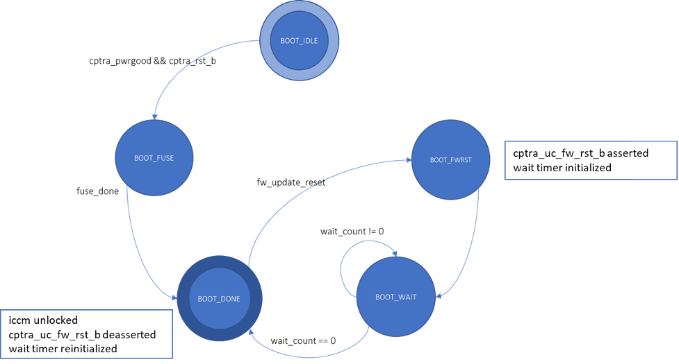 | |
| 46 | 46 | ||
| 47 | -After Caliptra comes out of global reset and enters the BOOT\_DONE state, a write to the fw\_update\_reset register triggers the FW update reset flow. In the BOOT\_FWRST state, only the reset to the VeeR core is asserted, ICCM is unlocked and the timer is initialized. After the timer expires, the FSM advances from the BOOT\_WAIT to BOOT\_DONE state where the reset is deasserted. | ||
| 48 | - | ||
| 49 | -| Control register | Start address | Description | | ||
| 50 | -| :------- | :---------- | :--------- | | ||
| 51 | -| FW_UPDATE_RESET | 0x30030418 | Register to trigger the FW update reset flow. Setting it to 1 starts the Boot FSM. The field auto-clears to 0. | | ||
| 52 | -| FW_UPDATE_RESET_WAIT_CYCLES | 0x3003041C | Programmable wait time to keep the microcontroller reset asserted. | | ||
| 53 | - | ||
| 47 | +Impactless firmware updates may be initiated by writing to the fw\_update\_reset register after Caliptra comes out of global reset and enters the BOOT\_DONE state. In the BOOT\_FWRST state, only the reset to the RISC-V core is asserted and the wait timer is initialized. After the timer expires, the FSM advances from the BOOT\_WAIT to BOOT\_DONE state where the reset is deasserted and ICCM is unlocked. | ||
| 54 | 48 | ||
| 55 | 49 | ## RISC-V core | |
| 56 | 50 | ||
| @@ -94,8 +88,8 @@ | |||
| 94 | 88 | ||
| 95 | 89 | The following table shows the memory map address ranges for each of the IP blocks in the cryptographic subsystem. | |
| 96 | 90 | ||
| 97 | -| IP/Peripheral | Slave \# | Address size | Start address | End address | | ||
| 98 | -| :---------------------------------- | :------- | :----------- | :------------ | :---------- | | ||
| 91 | +| IP/Peripheral | Target \# | Address size | Start address | End address | | ||
| 92 | +| :---------------------------------- | :-------- | :----------- | :------------ | :---------- | | ||
| 99 | 93 | | Cryptographic Initialization Engine | 0 | 32 KiB | 0x1000_0000 | 0x1000_7FFF | | |
| 100 | 94 | | ECC Secp384 | 1 | 32 KiB | 0x1000_8000 | 0x1000_FFFF | | |
| 101 | 95 | | HMAC384 | 2 | 4 KiB | 0x1001_0000 | 0x1001_0FFF | | |
| @@ -110,8 +104,8 @@ | |||
| 110 | 104 | ||
| 111 | 105 | The following table shows the memory map address ranges for each of the IP blocks in the peripherals’ subsystem. | |
| 112 | 106 | ||
| 113 | -| IP/Peripheral | Slave \# | Address size | Start address | End address | | ||
| 114 | -| :------------ | :------- | :----------- | :------------ | :---------- | | ||
| 107 | +| IP/Peripheral | Target \# | Address size | Start address | End address | | ||
| 108 | +| :------------ | :-------- | :----------- | :------------ | :---------- | | ||
| 115 | 109 | | QSPI | 7 | 4 KiB | 0x2000_0000 | 0x2000_0FFF | | |
| 116 | 110 | | UART | 8 | 4 KiB | 0x2000_1000 | 0x2000_1FFF | | |
| 117 | 111 | | CSRNG | 15 | 4 KiB | 0x2000_2000 | 0x2000_2FFF | | |
| @@ -122,8 +116,8 @@ | |||
| 122 | 116 | ||
| 123 | 117 | The following table shows the memory map address ranges for each of the IP blocks in the SoC interface subsystem. | |
| 124 | 118 | ||
| 125 | -| IP/Peripheral | Slave \# | Address size | Start address | End address | | ||
| 126 | -| :------------------------- | :------- | :----------- | :------------ | :---------- | | ||
| 119 | +| IP/Peripheral | Target \# | Address size | Start address | End address | | ||
| 120 | +| :------------------------- | :-------- | :----------- | :------------ | :---------- | | ||
| 127 | 121 | | Mailbox SRAM Direct Access | 10 | 128 KiB | 0x3000_0000 | 0x3001_FFFF | | |
| 128 | 122 | | Mailbox CSR | 10 | 4 KiB | 0x3002_0000 | 0x3002_0FFF | | |
| 129 | 123 | | SHA512 Accelerator CSR | 10 | 4 KiB | 0x3002_1000 | 0x3002_1FFF | | |
| @@ -134,8 +128,8 @@ | |||
| 134 | 128 | ||
| 135 | 129 | The following table shows the memory map address ranges for each of the local memory blocks that interface with RISC-V core. | |
| 136 | 130 | ||
| 137 | -| IP/Peripheral | Slave \# | Address size | Start address | End address | | ||
| 138 | -| :-------------- | :------- | :----------- | :------------ | :---------- | | ||
| 131 | +| IP/Peripheral | Target \# | Address size | Start address | End address | | ||
| 132 | +| :-------------- | :-------- | :----------- | :------------ | :---------- | | ||
| 139 | 133 | | ICCM0 (via DMA) | 12 | 128 KiB | 0x4000_0000 | 0x4001_FFFF | | |
| 140 | 134 | | DCCM | 11 | 128 KiB | 0x5000_0000 | 0x5001_FFFF | | |
| 141 | 135 | ||
| @@ -171,8 +165,8 @@ | |||
| 171 | 165 | | ECC (Notifications) | 4 | 7 | | |
| 172 | 166 | | HMAC (Errors) | 5 | 8 | | |
| 173 | 167 | | HMAC (Notifications) | 6 | 7 | | |
| 174 | -| KeyVault (Errors) | 7 | 8 | | ||
| 175 | -| KeyVault (Notifications) | 8 | 7 | | ||
| 168 | +| Key Vault (Errors) | 7 | 8 | | ||
| 169 | +| Key Vault (Notifications) | 8 | 7 | | ||
| 176 | 170 | | SHA512 (Errors) | 9 | 8 | | |
| 177 | 171 | | SHA512 (Notifications) | 10 | 7 | | |
| 178 | 172 | | SHA256 (Errors) | 11 | 8 | | |
| @@ -219,9 +213,9 @@ | |||
| 219 | 213 | ||
| 220 | 214 | ### AHB-lite interface | |
| 221 | 215 | ||
| 222 | -AHB-lite is a subset of the full AHB specification. It is primarily used in single master systems. This interface connects VeeR EL2 Core (LSU master) to the slave devices. See [Caliptra Core](#caliptra-core) for information. | ||
| 223 | - | ||
| 224 | -The interface can be customized to support variable address and data widths, and a variable number of slave devices. Each slave device is assigned an address range within the 32-bit address memory map region. The interface includes address decoding logic to route data to the appropriate AHB slave device based on the address specified. | ||
| 216 | +AHB-lite is a subset of the full AHB specification. It is primarily used in single initiator systems. This interface connects VeeR EL2 Core (LSU initiator) to the target devices. See [Caliptra Core](#caliptra-core) for information. | ||
| 217 | + | ||
| 218 | +The interface can be customized to support variable address and data widths, and a variable number of target devices. Each target device is assigned an address range within the 32-bit address memory map region. The interface includes address decoding logic to route data to the appropriate AHB target device based on the address specified. | ||
| 225 | 219 | ||
| 226 | 220 | The integration parameters for Caliptra’s AHB-lite interface are shown in the following table. | |
| 227 | 221 | ||
| @@ -449,7 +443,7 @@ | |||
| 449 | 443 | | CPTRA_CLK_GATING_EN | 0x300300bc | Register bit to enable or disable the clock gating feature. | | |
| 450 | 444 | ||
| 451 | 445 | ||
| 452 | -When enabled, halting the microcontroller turns off clocks to all of the cryptographic subsystem, the vaults (keyvault, PCR vault, and data vault), mailbox SRAM, SoC interface, and peripherals subsystem. The Watchdog timer and SoC registers run on the gated RDC clock. The RV core implements its own clock gating mechanism. Halting the core automatically turns off its clock. | ||
| 446 | +When enabled, halting the microcontroller turns off clocks to all of the cryptographic subsystem, the vaults (key vault, PCR vault, and data vault), mailbox SRAM, SoC interface, and peripherals subsystem. The Watchdog timer and SoC registers run on the gated RDC clock. The RV core implements its own clock gating mechanism. Halting the core automatically turns off its clock. | ||
| 453 | 447 | ||
| 454 | 448 | There are a total of 4 clocks in Caliptra: ungated clock, gated clock, gated RDC clock, and gated SoC IFC clock. The following table shows the different modules and their designated clocks. | |
| 455 | 449 | ||
| @@ -874,11 +868,16 @@ | |||
| 874 | 868 | | next | input | The core processes the rest of the message blocks using the result from the previous blocks. | | |
| 875 | 869 | | mode | input | Indicates the hash type of the function. This can be: <br> - SHA256/224 <br> - SHA256 | | |
| 876 | 870 | | zeroize | input | The core clears all internal registers to avoid any SCA information leakage. | | |
| 871 | +| WNTZ_MODE* | input | SHA256 core is configured in Winternitz verification mode. | | ||
| 872 | +| WNTZ_W\[3:0\]* | input | Winternitz W value. | | ||
| 873 | +| WNTZ_N_MODE* | input | Winternitz n value(SHA192/SHA256 --> n = 24/32) | | ||
| 877 | 874 | | block\[511:0\] | input | The input padded block of message. | | |
| 878 | 875 | | ready | output | When HIGH, the signal indicates the core is ready. | | |
| 879 | 876 | | digest\[255:0\] | output | The hashed value of the given block. | | |
| 880 | 877 | | digest_valid | output | When HIGH, the signal indicates the result is ready. | | |
| 881 | 878 | ||
| 879 | + | ||
| 880 | +\* For more imformation about these inputs, please refer to LMS accelerator section. | ||
| 882 | 881 | ||
| 883 | 882 | ### Address map | |
| 884 | 883 | ||
| @@ -1338,13 +1337,12 @@ | |||
| 1338 | 1337 | ||
| 1339 | 1338 | ##### KeyGen TVLA | |
| 1340 | 1339 | ||
| 1341 | -We detected a leakage using TVLA in the HMAC_DRBG algorithm during ECC key generation, based on 150,000 power traces. The leakage originated from a part of the SHA512 function (w_data) that was not fully protected by masking. The same leakage is expected for HMAC operations. | ||
| 1342 | - | ||
| 1343 | -*Figure 40: seed/nonce-dependent leakage detection using TVLA for ECC keygen after 150,000 traces* | ||
| 1340 | +The TVLA results for performing seed/nonce-dependent leakage detection using 200,000 traces is shown in the following figure. Based on this figure, there is no leakage in ECC keygen by changing the seed/nonce after 200,000 operations. | ||
| 1341 | + | ||
| 1342 | + | ||
| 1343 | +*Figure 40: seed/nonce-dependent leakage detection using TVLA for ECC keygen after 200,000 traces* | ||
| 1344 | 1344 | ||
| 1345 | 1345 |  | |
| 1346 | - | ||
| 1347 | -This leakage is very unlikely to occur in practice, even though it exists in TVLA results. Therefore, we will address it in the next release. | ||
| 1348 | 1346 | ||
| 1349 | 1347 | ##### Signing TVLA | |
| 1350 | 1348 | ||
| @@ -1389,6 +1387,75 @@ | |||
| 1389 | 1387 | | Signing | 932,990 | 2.332 | 428 | | |
| 1390 | 1388 | | Verifying | 1,223,938 | 3.060 | 326 | | |
| 1391 | 1389 | ||
| 1390 | + | ||
| 1391 | + | ||
| 1392 | +## LMS Accelerator | ||
| 1393 | + | ||
| 1394 | +LMS cryptography is a type of hash-based digital signature scheme that was standardized by NIST in 2020. It is based on the Leighton-Micali Signature (LMS) system, which uses a Merkle tree structure to combine many one-time signature (OTS) keys into a single public key. LMS cryptography is resistant to quantum attacks and can achieve a high level of security without relying on large integer mathematics. | ||
| 1395 | + | ||
| 1396 | +Caliptra supports only LMS verification using a software/hardware co-design approach. Hence, the LMS accelerator reuses the SHA256 engine to speedup the Winternitz chain by removing software-hardware interface overhead. The LMS-OTS verification algorithm is shown in follwoing figure: | ||
| 1397 | + | ||
| 1398 | +*Figure 43: LMS-OTS Verification algorithm* | ||
| 1399 | + | ||
| 1400 | + | ||
| 1401 | + | ||
| 1402 | +The high-level architecture of LMS is shown in the following figure. | ||
| 1403 | + | ||
| 1404 | +*Figure 44: LMS high-level architecture* | ||
| 1405 | + | ||
| 1406 | + | ||
| 1407 | + | ||
| 1408 | +### LMS parameters | ||
| 1409 | + | ||
| 1410 | +LMS parameters are shown in the following table: | ||
| 1411 | + | ||
| 1412 | +| Parameter | Description | Value | | ||
| 1413 | +| :-------- | :--------------------------------------------------------------------- | :------------------ | | ||
| 1414 | +| n | The number of bytes of the output of the hash function. | {24, 32} | | ||
| 1415 | +| w | The width (in bits) of the Winternitz coefficients. | {1, 2, 4, 8} | | ||
| 1416 | +| p | The number of n-byte string elements that make up the LM-OTS signature. | {265, 133, 67, 34} | | ||
| 1417 | +| H | A cryptographic hash function. | SHA256 | | ||
| 1418 | +| h | The height of the tree. | {5, 10, 15, 20, 25} | | ||
| 1419 | + | ||
| 1420 | + | ||
| 1421 | +- SHA256 is used for n=32 and SHA256/192 is used for n=24. | ||
| 1422 | +- SHAKE256 is not supported in this architecture. | ||
| 1423 | +- Value of p is determined based on w. If w=1, p is equal to 265, and so on. | ||
| 1424 | + | ||
| 1425 | +### Winternitz Chain Accelerator | ||
| 1426 | + | ||
| 1427 | +The Winternitz hash chain can be accelerated in hardware to enhance the performance of the design. For that, a configurable architecture is proposed that can reuse SHA256 engine. The LMS accelerator architecture is shown in the following figure, while H is SHA256 engine. | ||
| 1428 | + | ||
| 1429 | +*Figure 45: Winternitz chain architecture* | ||
| 1430 | + | ||
| 1431 | + | ||
| 1432 | + | ||
| 1433 | + | ||
| 1434 | +### Signal descriptions | ||
| 1435 | + | ||
| 1436 | +The LMS accelerator integrated into SHA256 architecture inputs and outputs are described as follows. | ||
| 1437 | + | ||
| 1438 | +| Name | Input or output | Description | | ||
| 1439 | +| :-------------- | :-------------- | :------------------------------------------------------------------------------------------- | | ||
| 1440 | +| clk | input | All signal timings are related to the rising edge of clk. | | ||
| 1441 | +| reset_n | input | The reset signal is active LOW and resets the core. This is the only active LOW signal. | | ||
| 1442 | +| init | input | The core is initialized and processes the first block of message. | | ||
| 1443 | +| next | input | The core processes the rest of the message blocks using the result from the previous blocks. | | ||
| 1444 | +| mode | input | Indicates the hash type of the function. This can be: <br> - SHA256/224 <br> - SHA256 | | ||
| 1445 | +| zeroize | input | The core clears all internal registers to avoid any SCA information leakage. | | ||
| 1446 | +| WNTZ_MODE | input | SHA256 core is configured in Winternitz verification mode. | | ||
| 1447 | +| WNTZ_W\[3:0\] | input | Winternitz W value. | | ||
| 1448 | +| WNTZ_N_MODE | input | Winternitz n value(SHA192/SHA256 --> n = 24/32) | | ||
| 1449 | +| block\[511:0\] | input | The input padded block of message. | | ||
| 1450 | +| ready | output | When HIGH, the signal indicates the core is ready. | | ||
| 1451 | +| digest\[255:0\] | output | The hashed value of the given block. | | ||
| 1452 | +| digest_valid | output | When HIGH, the signal indicates the result is ready. | | ||
| 1453 | + | ||
| 1454 | + | ||
| 1455 | +### Address map | ||
| 1456 | + | ||
| 1457 | +The address map for LMS accelerator integrated into SHA256 is shown here: [sha256\_reg — clp Reference (chipsalliance.github.io)](https://chipsalliance.github.io/caliptra-rtl/main/internal-regs/?p=clp.sha256_reg). | ||
| 1458 | + | ||
| 1392 | 1459 | ## PCR vault | |
| 1393 | 1460 | ||
| 1394 | 1461 | * Platform Configuration Register (PCR) vault is a register file that stores measurements to be used by the microcontroller. | |
| @@ -1426,9 +1493,9 @@ | |||
| 1426 | 1493 | Key Vault (KV) is a register file that stores the keys to be used by the microcontroller, but this register file is not observed by the microcontroller. Each cryptographic function has a control register and functional block designed to read from and write to the KV. | |
| 1427 | 1494 | ||
| 1428 | 1495 | | KV register | Description | | |
| 1429 | -| :------------------------------- | :------------------------------------------------------- | | ||
| 1430 | -| Key Control\[7:0\] | 8 Control registers, 32 bits each | | ||
| 1431 | -| Key Entry\[7:0\]\[15:0\]\[31:0\] | 8 Key entries, 512 bits each <br>No read or write access | | ||
| 1496 | +| :-------------------------------- | :-------------------------------------------------------- | | ||
| 1497 | +| Key Control\[31:0\] | 32 Control registers, 32 bits each | | ||
| 1498 | +| Key Entry\[31:0\]\[11:0\]\[31:0\] | 32 Key entries, 384 bits each <br>No read or write access | | ||
| 1432 | 1499 | ||
| 1433 | 1500 | ||
| 1434 | 1501 | ### Key vault functional block | |
| @@ -1456,13 +1523,17 @@ | |||
| 1456 | 1523 | ||
| 1457 | 1524 | A generic block is instantiated in each cryptographic block to enable access to KV. | |
| 1458 | 1525 | ||
| 1459 | -Each input to a cryptographic engine can have a key vault read block associated with it. The KV read block takes in a keyvault read control register that drives an FSM to copy an entry from the keyvault into the appropriate input register of the cryptographic engine. | ||
| 1460 | - | ||
| 1461 | -Each output generated by a cryptographic engine can have its result copied to a slot in the keyvault. The KV write block takes in a keyvault write control register. This register drives an FSM to copy the result from the cryptographic engine into the appropriate keyvault entry. It also programs a control field for that entry to indicate where that entry can be used. | ||
| 1526 | +Each input to a cryptographic engine can have a key vault read block associated with it. The KV read block takes in a key vault read control register that drives an FSM to copy an entry from the key vault into the appropriate input register of the cryptographic engine. | ||
| 1527 | + | ||
| 1528 | +Each output generated by a cryptographic engine can have its result copied to a slot in the key vault. The KV write block takes in a key vault write control register. This register drives an FSM to copy the result from the cryptographic engine into the appropriate key vault entry. It also programs a control field for that entry to indicate where that entry can be used. | ||
| 1462 | 1529 | ||
| 1463 | 1530 | After programming the key vault read control, FW needs to query the associated key vault read status to confirm that the requested key was copied successfully. After valid is set and the error field reports success, the key is ready to be used. | |
| 1464 | 1531 | ||
| 1465 | 1532 | Similarly, after programming the key vault write control and initiating the cryptographic function that generates the key to be written, FW needs to query the associated key vault write status to confirm that the requested key was generated and written successfully. | |
| 1533 | + | ||
| 1534 | +When a key is read from the key vault, the API register is locked and any result generated from the cryptographic block is not readable by firmware. The digest can only be sent to the key vault by appropriately programming the key vault write controls. After the cryptographic block completes its operation, the lock is cleared and the key is cleared from the API registers. | ||
| 1535 | + | ||
| 1536 | +If multiple iterations of the cryptographic function are required, the key vault read and write controls must be programmed for each iteration. This ensures that the lock is set and the digest is not readable. | ||
| 1466 | 1537 | ||
| 1467 | 1538 | The following tables describe read, write, and status values for key vault blocks. | |
| 1468 | 1539 | ||
| @@ -1522,10 +1593,10 @@ | |||
| 1522 | 1593 | The following tables describe DOE register and control fields. | |
| 1523 | 1594 | ||
| 1524 | 1595 | | DOE Register | Address | Description | | |
| 1525 | -| :----------- | :--------- | :----------------------------------------------------------------------------------------------------------------------------- | | ||
| 1596 | +| :----------- | :--------- | :------------------------------------------------------------------------------------------------------------------------------ | | ||
| 1526 | 1597 | | IV | 0x10000000 | 128 bit IV for DOE flow. Stored in big-endian representation. | | |
| 1527 | 1598 | | CTRL | 0x10000010 | Controls for DOE flows. | | |
| 1528 | -| STATUS | 0x10000014 | Valid indicates the command is done and results are stored in keyvault. Ready indicates the core is ready for another command. | | ||
| 1599 | +| STATUS | 0x10000014 | Valid indicates the command is done and results are stored in key vault. Ready indicates the core is ready for another command. | | ||
| 1529 | 1600 | ||
| 1530 | 1601 | ||
| 1531 | 1602 | | DOE Ctrl Fields | Reset | Description | | |
| @@ -1558,8 +1629,9 @@ | |||
| 1558 | 1629 | The following table describes cryptographic errors. | |
| 1559 | 1630 | ||
| 1560 | 1631 | | Errors | Error type | Description | | |
| 1561 | -| :--------- | :----------------- | :-------------------------------------------------------------------------------------------------------------------------------------------------------- | | ||
| 1632 | +| :----------- | :----------------- | :-------------------------------------------------------------------------------------------------------------------------------------------------------- | | ||
| 1562 | 1633 | | ECC_R_ZERO | HW_ERROR_NON_FATAL | Indicates a non-fatal error in ECC signing if the computed signature R is equal to 0. FW should change the message or privkey to perform a valid signing. | | |
| 1634 | +| CRYPTO_ERROR | HW_ERROR_FATAL | Indicates a fatal error due to multiple cryptographic operations occurring simultaneously. FW must only operate one cryptographic engine at a time. | | ||
| 1563 | 1635 | ||
| 1564 | 1636 | ||
| 1565 | 1637 | # Terminology | |
Image not present in this version
Image not present in this version

Image not present in this version